Embed Size (px)
Citation preview
Product
Folder
Sample &Buy
Technical
Documents
Tools &
Software
Support &Community
ReferenceDesign
CC2540TSWRS172A –JULY 2014–REVISED NOVEMBER 2015
CC2540T Extended Industrial Temperature Bluetooth® Smart Wireless MCU1 Device Overview
1.1 Features1
• True Single-Chip BLE Solution: CC2540T Can Run • PeripheralsBoth Application and BLE Protocol Stack, Includes – 12-Bit ADC With Eight Channels andPeripherals to Interface With Wide Range of Configurable ResolutionSensors, and so forth – Integrated Ultralow-Power Comparator
• Operating Temperature up to 125°C – General-Purpose Timers (One 16-Bit, Two 8-Bit)• 6-mm × 6-mm Package – 21 General-Purpose I/O (GPIO) Pins• RF (19 × 4 mA, 2 × 20 mA)
– Bluetooth® Low Energy Technology Compatible – 32-kHz Sleep Timer With Capture– Excellent Link Budget (up to 97 dB), Enabling – Two Powerful USARTs With Support for Several
Long-Range Applications Without External Front Serial ProtocolsEnd – Full-Speed USB Interface
– Accurate Digital Received Signal-Strength – IR Generation CircuitryIndicator (RSSI) – Powerful Five-Channel DMA
– Suitable for Systems Targeting Compliance With – AES Security CoprocessorWorldwide Radio Frequency Regulations:– Battery Monitor and Temperature Sensor• ETSI EN 300 328 and EN 300 440 Class 2– Each CC2540T Contains a Unique 48-Bit IEEE(Europe)
Address• FCC CFR47 Part 15 (US) • Bluetooth v4.0 Compliant Protocol Stack for• ARIB STD-T66 (Japan) Single-Mode BLE Solution• Layout – Complete Power-Optimized Stack, Including
– Few External Components Controller and Host– Reference Design Provided • GAP: Central, Peripheral, Observer, or– 6-mm × 6-mm VQFN40 Package Broadcaster (Including Combination Roles)
• Low Power • ATT and GATT: Client and Server– Active Mode RX Down to 19.6 mA • SMP: AES-128 Encryption and Decryption– Active Mode TX (–6 dBm): 24 mA • L2CAP– Power Mode 1 (3-μs Wake Up): 235 μA – Sample Applications and Profiles– Power Mode 2 (Sleep Timer On): 0.9 μA • Generic Applications for GAP Central and– Power Mode 3 (External Interrupts): 0.4 μA Peripheral Roles– Wide Supply Voltage Range (2 V–3.6 V) • Proximity, Accelerometer, Simple Keys, and
Battery GATT Services– Full RAM and Register Retention in All PowerModes – Multiple Configuration Options
• TPS62730 Compatible, • Single-Chip Configuration, AllowingLow Power in Active Mode Application to Run on CC2540T– RX Down to 15.8 mA (3-V Supply) • Network Processor Interface for Applications
Running on an External Microcontroller– TX (–6 dBm): 18.6 mA (3-V Supply)– BTool: Windows PC Application for Evaluation,• Microcontroller
Development, and Test– High-Performance and Low-Power 8051• Development ToolsMicrocontroller Core
– CC2540T Mini Development Kit– 256KB of In-System-Programmable Flash– SmartRF™ Software– 8KB of SRAM– Supported by IAR Embedded Workbench™
Software for 8051
1
An IMPORTANT NOTICE at the end of this data sheet addresses availability, warranty, changes, use in safety-critical applications,intellectual property matters and other important disclaimers. PRODUCTION DATA.
CC2540TSWRS172A –JULY 2014–REVISED NOVEMBER 2015 www.ti.com
1.2 Applications• 2.4-GHz Bluetooth Low Energy Systems • Power Tools• Lighting • Maintenance• Motor Monitoring • Wireless HMI and Remote Display• Proximity Sensing • USB Dongles• Cable Replacement • Smart Phone Connectivity
1.3 DescriptionThe CC2540T device is a cost-effective, low-power, true wireless MCU for Bluetooth low energyapplications. The CC2540T enables robust BLE master or slave nodes to be built with very low total bill-of-material costs, and it can operate up to 125°C. The CC2540T combines an excellent RF transceiver withan industry-standard enhanced 8051 MCU, in-system programmable flash memory, 8KB of RAM, andmany other powerful supporting features and peripherals. The CC2540T is suitable for systems wherevery low power consumption is required. Very low-power sleep modes are available. Short transition timesbetween operating modes further enable low power consumption.
Combined with the Bluetooth low energy protocol stack from Texas Instruments, the CC2540TF256 formsthe market’s most flexible and cost-effective single-mode Bluetooth low energy solution.
Table 1-1. Device Information (1)
PART NUMBER PACKAGE BODY SIZE (NOM)CC2540TF256RHAR VQFN (40) 6.00 mm × 6.00 mmCC2540TF256RHAT VQFN (40) 6.00 mm × 6.00 mm
(1) For more information, see Section 8, Mechanical Packaging and Orderable Information.
2 Device Overview Copyright © 2014–2015, Texas Instruments IncorporatedSubmit Documentation FeedbackProduct Folder Links: CC2540T
RESETWATCHDOG
TIMER
IRQ CTRL FLASH CTRL
DEBUGINTERFACE
CLOCK MUXand
CALIBRATION
DMA
8051 CPUCORE
32-MHz
CRYSTAL OSC
OP-AMP
32.768-kHz
CRYSTAL OSC
HIGH-
SPEED
RC-OSC POWER MANAGEMENT CONTROLLER
USART 0
USB
USART 1
TIMER 1 (16-Bit)
TIMER 3 (8-Bit)
TIMER 4 (8-Bit)
TIMER 2(BLE LL TIMER)
FLASH
FIFOCTRL 1 KB SRAM
ON-CHIP VOLTAGE
REGULATOR
POWER-ON RESET
BROWN OUT
VDD (2 V–3.6 V)
DCOUPLRESET_N
XOSC_Q2
XOSC_Q1
P2_4
P1_7
P0_7
P2_3
P1_6
P0_6
P2_2
P1_5
P0_5
P1_2
P0_2
P2_1
P1_4
P0_4
P1_1
P0_1
P2_0
P1_3
P0_3
P1_0
P0_0
MODULATORDEMODULATOR
RECEIVE TRANSMIT
FR
EQ
UE
NC
Y
SY
NT
HE
SIZ
ER
SY
NT
H
RF_P RF_N
B0301-05
RADIO REGISTERS
SF
R B
us
SF
R B
us
DS
ADC
AUDIO/DC
AESENCRYPTION
ANDDECRYPTION
MEMORYARBITRATOR FLASH
UNIFIED
SFR
IRAM
XRAM
PDATA
SLEEP TIMER
32-kHz
RC-OSC
I/O
CO
NT
RO
LL
ER
DIGITAL
ANALOG
MIXED
ANALOG COMPARATOR
USB_N
USB_P
Radio
Arb
iter
Link Layer Engine
CC2540Twww.ti.com SWRS172A –JULY 2014–REVISED NOVEMBER 2015
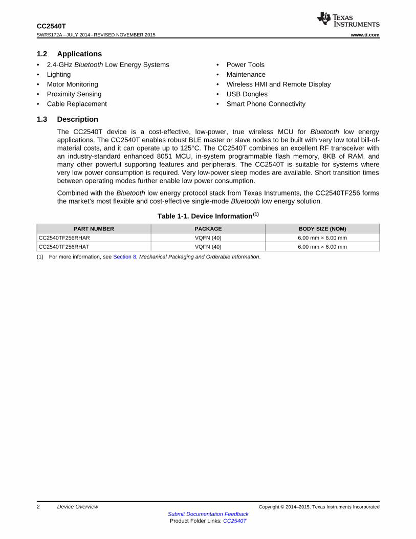
1.4 Functional Block DiagramFigure 1-1 shows the functional block diagram of the CC2540T device.
Figure 1-1. Functional Block Diagram
Copyright © 2014–2015, Texas Instruments Incorporated Device Overview 3Submit Documentation FeedbackProduct Folder Links: CC2540T
CC2540TSWRS172A –JULY 2014–REVISED NOVEMBER 2015 www.ti.com
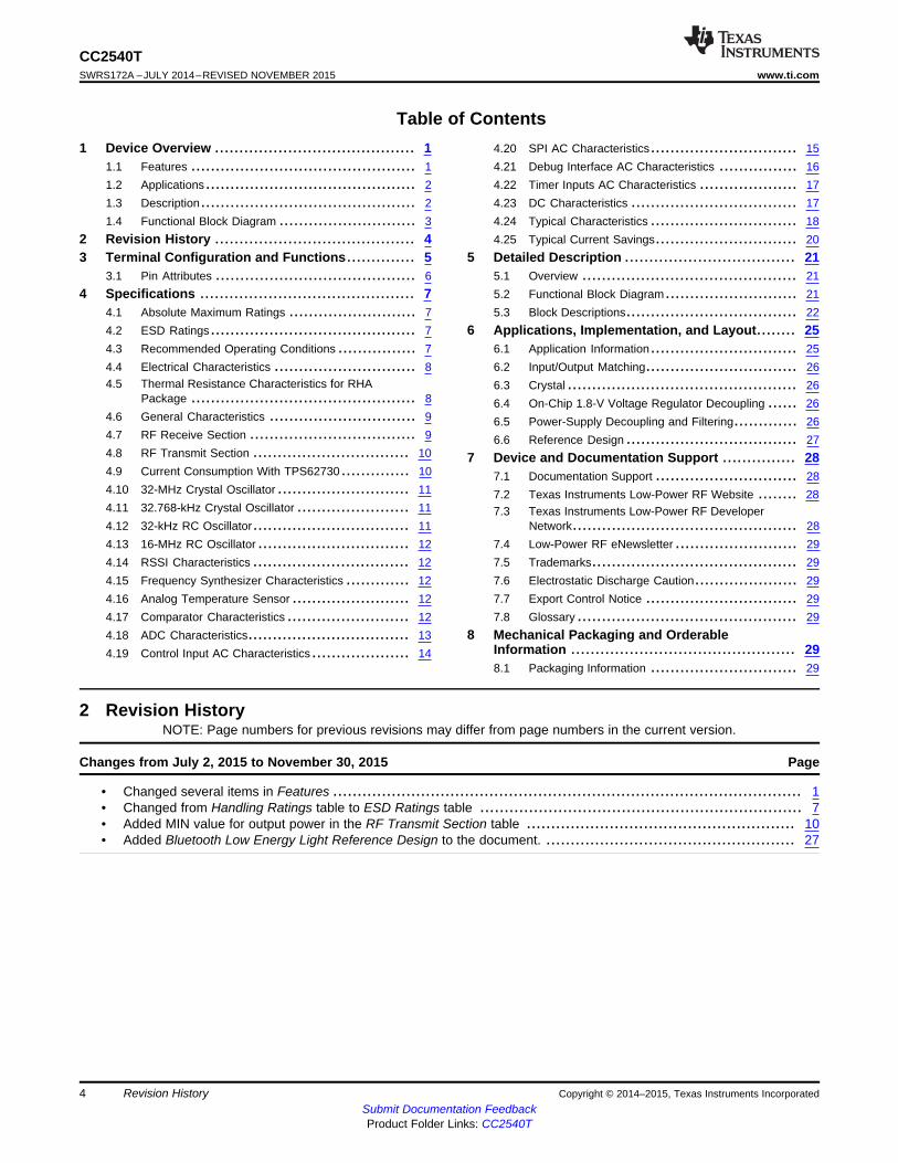
Table of Contents1 Device Overview ......................................... 1 4.20 SPI AC Characteristics.............................. 15
1.1 Features .............................................. 1 4.21 Debug Interface AC Characteristics ................ 161.2 Applications........................................... 2 4.22 Timer Inputs AC Characteristics .................... 171.3 Description............................................ 2 4.23 DC Characteristics .................................. 171.4 Functional Block Diagram ............................ 3 4.24 Typical Characteristics .............................. 18
2 Revision History ......................................... 4 4.25 Typical Current Savings............................. 203 Terminal Configuration and Functions.............. 5 5 Detailed Description ................................... 21
3.1 Pin Attributes ......................................... 6 5.1 Overview ............................................ 214 Specifications ............................................ 7 5.2 Functional Block Diagram........................... 21
4.1 Absolute Maximum Ratings .......................... 7 5.3 Block Descriptions................................... 224.2 ESD Ratings.......................................... 7 6 Applications, Implementation, and Layout........ 254.3 Recommended Operating Conditions ................ 7 6.1 Application Information.............................. 254.4 Electrical Characteristics ............................. 8 6.2 Input/Output Matching............................... 264.5 Thermal Resistance Characteristics for RHA 6.3 Crystal ............................................... 26
Package .............................................. 8 6.4 On-Chip 1.8-V Voltage Regulator Decoupling ...... 264.6 General Characteristics .............................. 9 6.5 Power-Supply Decoupling and Filtering............. 264.7 RF Receive Section .................................. 9 6.6 Reference Design ................................... 274.8 RF Transmit Section ................................ 10 7 Device and Documentation Support ............... 284.9 Current Consumption With TPS62730.............. 10 7.1 Documentation Support ............................. 284.10 32-MHz Crystal Oscillator ........................... 11 7.2 Texas Instruments Low-Power RF Website ........ 284.11 32.768-kHz Crystal Oscillator ....................... 11 7.3 Texas Instruments Low-Power RF Developer4.12 32-kHz RC Oscillator................................ 11 Network.............................................. 284.13 16-MHz RC Oscillator ............................... 12 7.4 Low-Power RF eNewsletter ......................... 294.14 RSSI Characteristics ................................ 12 7.5 Trademarks.......................................... 294.15 Frequency Synthesizer Characteristics ............. 12 7.6 Electrostatic Discharge Caution..................... 294.16 Analog Temperature Sensor ........................ 12 7.7 Export Control Notice ............................... 294.17 Comparator Characteristics ......................... 12 7.8 Glossary ............................................. 294.18 ADC Characteristics................................. 13 8 Mechanical Packaging and Orderable
Information .............................................. 294.19 Control Input AC Characteristics.................... 148.1 Packaging Information .............................. 29
2 Revision HistoryNOTE: Page numbers for previous revisions may differ from page numbers in the current version.
Changes from July 2, 2015 to November 30, 2015 Page
• Changed several items in Features ................................................................................................ 1• Changed from Handling Ratings table to ESD Ratings table .................................................................. 7• Added MIN value for output power in the RF Transmit Section table ....................................................... 10• Added Bluetooth Low Energy Light Reference Design to the document. ................................................... 27
4 Revision History Copyright © 2014–2015, Texas Instruments IncorporatedSubmit Documentation FeedbackProduct Folder Links: CC2540T
P0_1
RE
SE
T_N
P2_3 / X
OS
C32K
_Q
2
AV
DD
6
DVDD_USB
R_BIAS
P0_2
P0_0
AVDD4
P0_3
AVDD1
P0_4
AVDD2
P0_5RF_N
P0_6
RF_P
P0_7
AVDD3
XOSC_Q1
P1_0
XOSC_Q2
AVDD5
P2_2
P2_4 / X
OS
C32K
_Q
1
USB_P
P2_1
USB_N
P2_0
DGND_USB
P1_7
P1_5
P1_6
P1_4
DV
DD
1
P1_3
P1_1
DC
OU
PL
P1_2
DVDD2
P0076-05
301
292
283
274
265
256
24
22
7
9
23
21
8
1018 20
33 31
17 19
34 32
16
35
15
36
14
37
13
38
12
39
11
40
GNDGround Pad
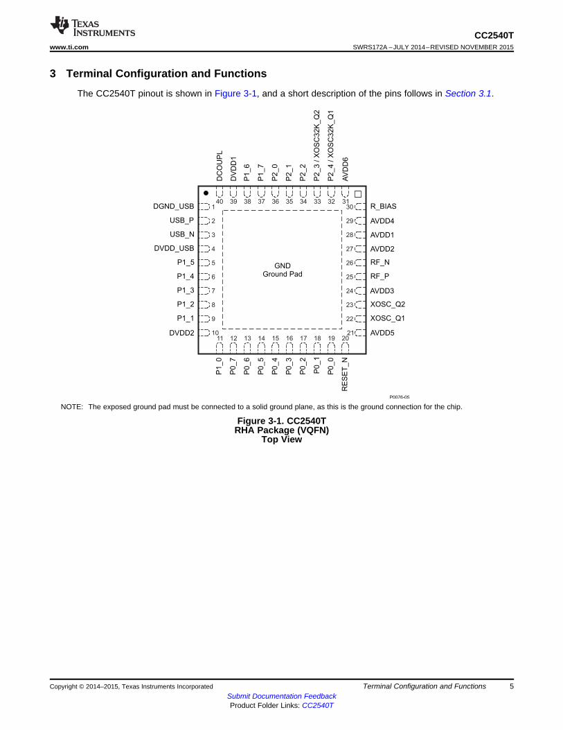
CC2540Twww.ti.com SWRS172A –JULY 2014–REVISED NOVEMBER 2015
3 Terminal Configuration and Functions
The CC2540T pinout is shown in Figure 3-1, and a short description of the pins follows in Section 3.1.
NOTE: The exposed ground pad must be connected to a solid ground plane, as this is the ground connection for the chip.
Figure 3-1. CC2540TRHA Package (VQFN)
Top View
Copyright © 2014–2015, Texas Instruments Incorporated Terminal Configuration and Functions 5Submit Documentation FeedbackProduct Folder Links: CC2540T
CC2540TSWRS172A –JULY 2014–REVISED NOVEMBER 2015 www.ti.com
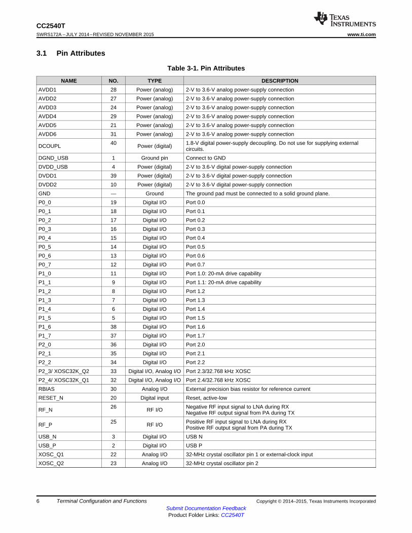
3.1 Pin Attributes
Table 3-1. Pin Attributes
NAME NO. TYPE DESCRIPTIONAVDD1 28 Power (analog) 2-V to 3.6-V analog power-supply connectionAVDD2 27 Power (analog) 2-V to 3.6-V analog power-supply connectionAVDD3 24 Power (analog) 2-V to 3.6-V analog power-supply connectionAVDD4 29 Power (analog) 2-V to 3.6-V analog power-supply connectionAVDD5 21 Power (analog) 2-V to 3.6-V analog power-supply connectionAVDD6 31 Power (analog) 2-V to 3.6-V analog power-supply connection
40 1.8-V digital power-supply decoupling. Do not use for supplying externalDCOUPL Power (digital) circuits.DGND_USB 1 Ground pin Connect to GNDDVDD_USB 4 Power (digital) 2-V to 3.6-V digital power-supply connectionDVDD1 39 Power (digital) 2-V to 3.6-V digital power-supply connectionDVDD2 10 Power (digital) 2-V to 3.6-V digital power-supply connectionGND — Ground The ground pad must be connected to a solid ground plane.P0_0 19 Digital I/O Port 0.0P0_1 18 Digital I/O Port 0.1P0_2 17 Digital I/O Port 0.2P0_3 16 Digital I/O Port 0.3P0_4 15 Digital I/O Port 0.4P0_5 14 Digital I/O Port 0.5P0_6 13 Digital I/O Port 0.6P0_7 12 Digital I/O Port 0.7P1_0 11 Digital I/O Port 1.0: 20-mA drive capabilityP1_1 9 Digital I/O Port 1.1: 20-mA drive capabilityP1_2 8 Digital I/O Port 1.2P1_3 7 Digital I/O Port 1.3P1_4 6 Digital I/O Port 1.4P1_5 5 Digital I/O Port 1.5P1_6 38 Digital I/O Port 1.6P1_7 37 Digital I/O Port 1.7P2_0 36 Digital I/O Port 2.0P2_1 35 Digital I/O Port 2.1P2_2 34 Digital I/O Port 2.2P2_3/ XOSC32K_Q2 33 Digital I/O, Analog I/O Port 2.3/32.768 kHz XOSCP2_4/ XOSC32K_Q1 32 Digital I/O, Analog I/O Port 2.4/32.768 kHz XOSCRBIAS 30 Analog I/O External precision bias resistor for reference currentRESET_N 20 Digital input Reset, active-low
26 Negative RF input signal to LNA during RXRF_N RF I/O Negative RF output signal from PA during TX25 Positive RF input signal to LNA during RXRF_P RF I/O Positive RF output signal from PA during TX
USB_N 3 Digital I/O USB NUSB_P 2 Digital I/O USB PXOSC_Q1 22 Analog I/O 32-MHz crystal oscillator pin 1 or external-clock inputXOSC_Q2 23 Analog I/O 32-MHz crystal oscillator pin 2
6 Terminal Configuration and Functions Copyright © 2014–2015, Texas Instruments IncorporatedSubmit Documentation FeedbackProduct Folder Links: CC2540T
CC2540Twww.ti.com SWRS172A –JULY 2014–REVISED NOVEMBER 2015
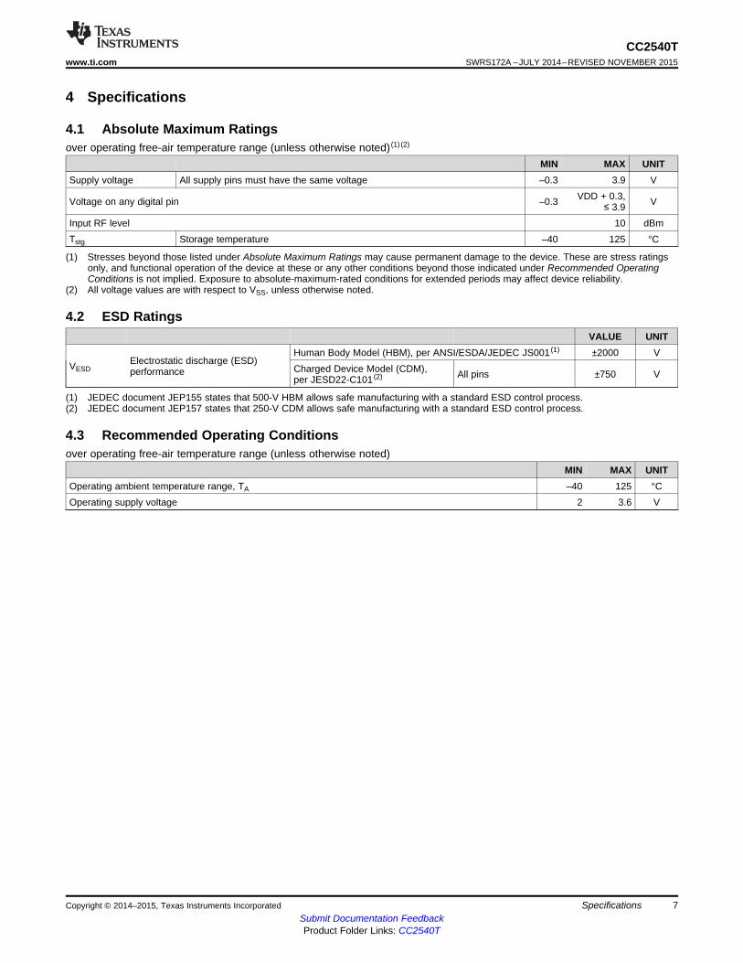
4 Specifications
4.1 Absolute Maximum Ratingsover operating free-air temperature range (unless otherwise noted) (1) (2)
MIN MAX UNITSupply voltage All supply pins must have the same voltage –0.3 3.9 V
VDD + 0.3,Voltage on any digital pin –0.3 V≤ 3.9Input RF level 10 dBmTstg Storage temperature –40 125 °C
(1) Stresses beyond those listed under Absolute Maximum Ratings may cause permanent damage to the device. These are stress ratingsonly, and functional operation of the device at these or any other conditions beyond those indicated under Recommended OperatingConditions is not implied. Exposure to absolute-maximum-rated conditions for extended periods may affect device reliability.
(2) All voltage values are with respect to VSS, unless otherwise noted.
4.2 ESD RatingsVALUE UNIT
Human Body Model (HBM), per ANSI/ESDA/JEDEC JS001 (1) ±2000 VElectrostatic discharge (ESD)VESD Charged Device Model (CDM),performance All pins ±750 Vper JESD22-C101 (2)
(1) JEDEC document JEP155 states that 500-V HBM allows safe manufacturing with a standard ESD control process.(2) JEDEC document JEP157 states that 250-V CDM allows safe manufacturing with a standard ESD control process.
4.3 Recommended Operating Conditionsover operating free-air temperature range (unless otherwise noted)
MIN MAX UNITOperating ambient temperature range, TA –40 125 °COperating supply voltage 2 3.6 V
Copyright © 2014–2015, Texas Instruments Incorporated Specifications 7Submit Documentation FeedbackProduct Folder Links: CC2540T
CC2540TSWRS172A –JULY 2014–REVISED NOVEMBER 2015 www.ti.com
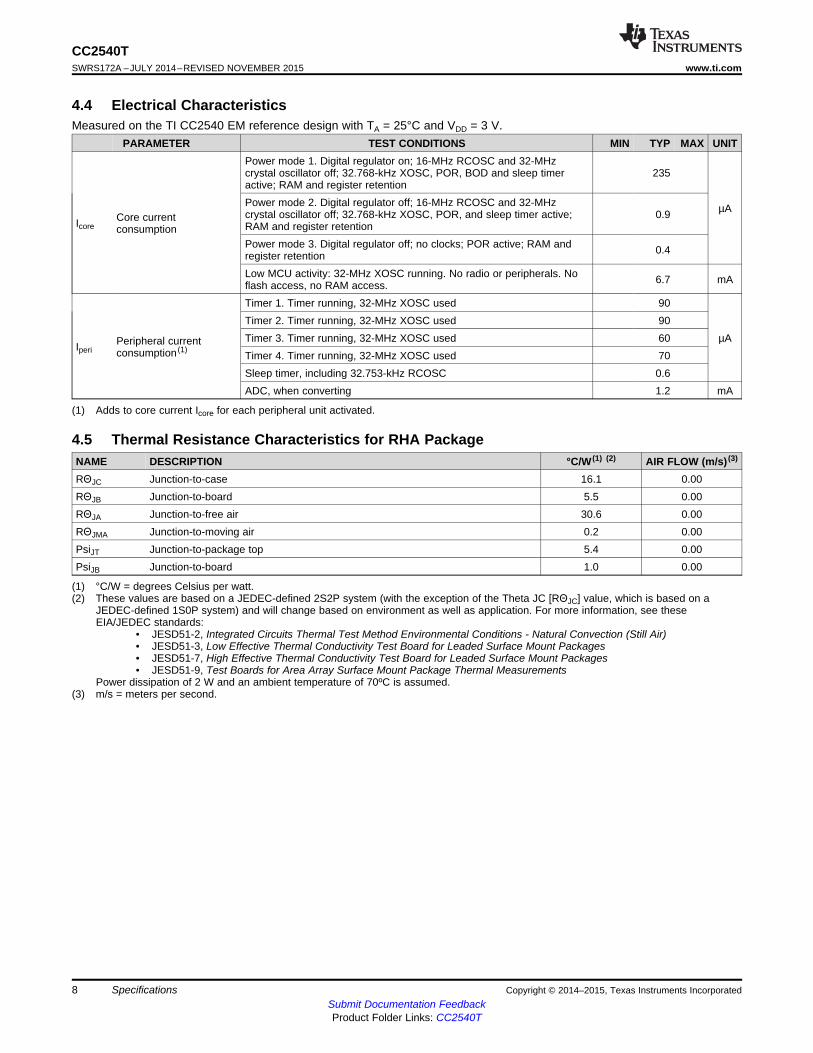
4.4 Electrical CharacteristicsMeasured on the TI CC2540 EM reference design with TA = 25°C and VDD = 3 V.
PARAMETER TEST CONDITIONS MIN TYP MAX UNITPower mode 1. Digital regulator on; 16-MHz RCOSC and 32-MHzcrystal oscillator off; 32.768-kHz XOSC, POR, BOD and sleep timer 235active; RAM and register retentionPower mode 2. Digital regulator off; 16-MHz RCOSC and 32-MHz µAcrystal oscillator off; 32.768-kHz XOSC, POR, and sleep timer active; 0.9Core currentIcore RAM and register retentionconsumptionPower mode 3. Digital regulator off; no clocks; POR active; RAM and 0.4register retentionLow MCU activity: 32-MHz XOSC running. No radio or peripherals. No 6.7 mAflash access, no RAM access.Timer 1. Timer running, 32-MHz XOSC used 90Timer 2. Timer running, 32-MHz XOSC used 90Timer 3. Timer running, 32-MHz XOSC used 60 µAPeripheral currentIperi consumption (1) Timer 4. Timer running, 32-MHz XOSC used 70Sleep timer, including 32.753-kHz RCOSC 0.6ADC, when converting 1.2 mA
(1) Adds to core current Icore for each peripheral unit activated.
4.5 Thermal Resistance Characteristics for RHA PackageNAME DESCRIPTION °C/W (1) (2) AIR FLOW (m/s) (3)
RΘJC Junction-to-case 16.1 0.00RΘJB Junction-to-board 5.5 0.00RΘJA Junction-to-free air 30.6 0.00RΘJMA Junction-to-moving air 0.2 0.00PsiJT Junction-to-package top 5.4 0.00PsiJB Junction-to-board 1.0 0.00
(1) °C/W = degrees Celsius per watt.(2) These values are based on a JEDEC-defined 2S2P system (with the exception of the Theta JC [RΘJC] value, which is based on a
JEDEC-defined 1S0P system) and will change based on environment as well as application. For more information, see theseEIA/JEDEC standards:
• JESD51-2, Integrated Circuits Thermal Test Method Environmental Conditions - Natural Convection (Still Air)• JESD51-3, Low Effective Thermal Conductivity Test Board for Leaded Surface Mount Packages• JESD51-7, High Effective Thermal Conductivity Test Board for Leaded Surface Mount Packages• JESD51-9, Test Boards for Area Array Surface Mount Package Thermal Measurements
Power dissipation of 2 W and an ambient temperature of 70ºC is assumed.(3) m/s = meters per second.
8 Specifications Copyright © 2014–2015, Texas Instruments IncorporatedSubmit Documentation FeedbackProduct Folder Links: CC2540T
CC2540Twww.ti.com SWRS172A –JULY 2014–REVISED NOVEMBER 2015
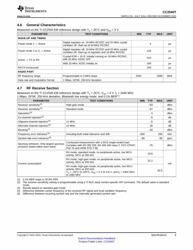
4.6 General CharacteristicsMeasured on the TI CC2540 EM reference design with TA = 25°C and VDD = 3 V.
PARAMETER TEST CONDITIONS MIN TYP MAX UNITWAKE-UP AND TIMING
Digital regulator on, 16-MHz RCOSC and 32-MHz crystalPower mode 1 → Active 4 µsoscillator off. Start-up of 16-MHz RCOSCDigital regulator off, 16-MHz RCOSC and 32-MHz crystalPower mode 2 or 3 → Active 120 µsoscillator off. Start-up of regulator and 16-MHz RCOSCCrystal ESR = 16 Ω. Initially running on 16-MHz RCOSC, 410 µswith 32-MHz XOSC OFFActive → TX or RXWith 32-MHz XOSC initially on 160 µs
RX/TX turnaround 150 µsRADIO PARTRF frequency range Programmable in 2-MHz steps 2402 2480 MHzData rate and modulation format 1 Mbps, GFSK, 250-kHz deviation
4.7 RF Receive SectionMeasured on the TI CC2540 EM reference design with TA = 25°C, VDD = 3 V, fc = 2440 MHz1 Mbps, GFSK, 250-kHz deviation, Bluetooth low energy mode, and 0.1% BER (1).
PARAMETER TEST CONDITIONS MIN TYP MAX UNITReceiver sensitivity (2) High-gain mode –93 dBmReceiver sensitivity (2) Standard mode –87 dBmSaturation (3) 6 dBmCo-channel rejection (3) –5 dBAdjacent-channel rejection (3) ±1 MHz –5 dBAlternate-channel rejection (3) ±2 MHz 30 dBBlocking (3) –30 dBmFrequency error tolerance (4) Including both initial tolerance and drift –250 250 kHzSymbol rate error tolerance (5) –80 80 ppm
Conducted measurement with a 50-Ω single-ended load.Spurious emission. Only largest spurious Complies with EN 300 328, EN 300 440 class 2, FCC CFR47, –75 dBmemission stated within each band. Part 15 and ARIB STD-T-66RX mode, standard mode, no peripherals active, low MCU 19.6activity, MCU at 250 kHzRX mode, high-gain mode, no peripherals active, low MCU 22.1activity, MCU at 250 kHzCurrent consumption mARX mode, high-gain mode, no peripherals active, low MCUactivity, MCU at 250 kHz; 30.5TA = –40°C to 125°C, VDD = 2 V to 3.6 V, and fc = 2402 MHzto 2480 MHz
(1) 0.1% BER maps to 30.8% PER(2) The receiver sensitivity setting is programmable using a TI BLE stack vendor-specific API command. The default value is standard
mode.(3) Results based on standard gain mode(4) Difference between center frequency of the received RF signal and local oscillator frequency(5) Difference between incoming symbol rate and the internally generated symbol rate
Copyright © 2014–2015, Texas Instruments Incorporated Specifications 9Submit Documentation FeedbackProduct Folder Links: CC2540T
CC2540TSWRS172A –JULY 2014–REVISED NOVEMBER 2015 www.ti.com
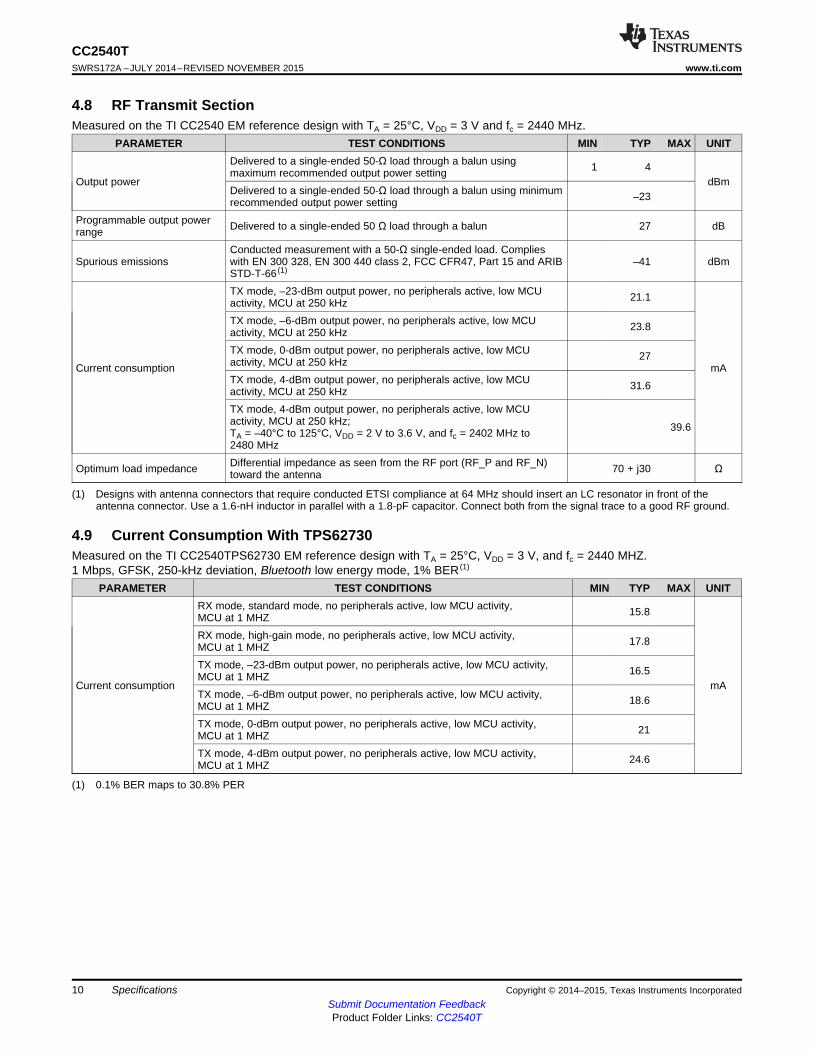
4.8 RF Transmit SectionMeasured on the TI CC2540 EM reference design with TA = 25°C, VDD = 3 V and fc = 2440 MHz.
PARAMETER TEST CONDITIONS MIN TYP MAX UNITDelivered to a single-ended 50-Ω load through a balun using 1 4maximum recommended output power setting
Output power dBmDelivered to a single-ended 50-Ω load through a balun using minimum –23recommended output power setting
Programmable output power Delivered to a single-ended 50 Ω load through a balun 27 dBrangeConducted measurement with a 50-Ω single-ended load. Complies
Spurious emissions with EN 300 328, EN 300 440 class 2, FCC CFR47, Part 15 and ARIB –41 dBmSTD-T-66 (1)
TX mode, –23-dBm output power, no peripherals active, low MCU 21.1activity, MCU at 250 kHzTX mode, –6-dBm output power, no peripherals active, low MCU 23.8activity, MCU at 250 kHzTX mode, 0-dBm output power, no peripherals active, low MCU 27activity, MCU at 250 kHzCurrent consumption mATX mode, 4-dBm output power, no peripherals active, low MCU 31.6activity, MCU at 250 kHzTX mode, 4-dBm output power, no peripherals active, low MCUactivity, MCU at 250 kHz; 39.6TA = –40°C to 125°C, VDD = 2 V to 3.6 V, and fc = 2402 MHz to2480 MHzDifferential impedance as seen from the RF port (RF_P and RF_N)Optimum load impedance 70 + j30 Ωtoward the antenna
(1) Designs with antenna connectors that require conducted ETSI compliance at 64 MHz should insert an LC resonator in front of theantenna connector. Use a 1.6-nH inductor in parallel with a 1.8-pF capacitor. Connect both from the signal trace to a good RF ground.
4.9 Current Consumption With TPS62730Measured on the TI CC2540TPS62730 EM reference design with TA = 25°C, VDD = 3 V, and fc = 2440 MHZ.1 Mbps, GFSK, 250-kHz deviation, Bluetooth low energy mode, 1% BER (1)
PARAMETER TEST CONDITIONS MIN TYP MAX UNITRX mode, standard mode, no peripherals active, low MCU activity, 15.8MCU at 1 MHZRX mode, high-gain mode, no peripherals active, low MCU activity, 17.8MCU at 1 MHZTX mode, –23-dBm output power, no peripherals active, low MCU activity, 16.5MCU at 1 MHZ
Current consumption mATX mode, –6-dBm output power, no peripherals active, low MCU activity, 18.6MCU at 1 MHZTX mode, 0-dBm output power, no peripherals active, low MCU activity, 21MCU at 1 MHZTX mode, 4-dBm output power, no peripherals active, low MCU activity, 24.6MCU at 1 MHZ
(1) 0.1% BER maps to 30.8% PER
10 Specifications Copyright © 2014–2015, Texas Instruments IncorporatedSubmit Documentation FeedbackProduct Folder Links: CC2540T
CC2540Twww.ti.com SWRS172A –JULY 2014–REVISED NOVEMBER 2015
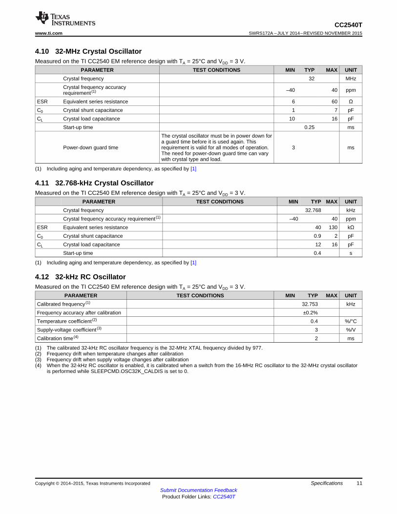
4.10 32-MHz Crystal OscillatorMeasured on the TI CC2540 EM reference design with TA = 25°C and VDD = 3 V.
PARAMETER TEST CONDITIONS MIN TYP MAX UNITCrystal frequency 32 MHzCrystal frequency accuracy –40 40 ppmrequirement (1)
ESR Equivalent series resistance 6 60 ΩC0 Crystal shunt capacitance 1 7 pFCL Crystal load capacitance 10 16 pF
Start-up time 0.25 msThe crystal oscillator must be in power down fora guard time before it is used again. This
Power-down guard time requirement is valid for all modes of operation. 3 msThe need for power-down guard time can varywith crystal type and load.
(1) Including aging and temperature dependency, as specified by [1]
4.11 32.768-kHz Crystal OscillatorMeasured on the TI CC2540 EM reference design with TA = 25°C and VDD = 3 V.
PARAMETER TEST CONDITIONS MIN TYP MAX UNITCrystal frequency 32.768 kHzCrystal frequency accuracy requirement (1) –40 40 ppm
ESR Equivalent series resistance 40 130 kΩC0 Crystal shunt capacitance 0.9 2 pFCL Crystal load capacitance 12 16 pF
Start-up time 0.4 s
(1) Including aging and temperature dependency, as specified by [1]
4.12 32-kHz RC OscillatorMeasured on the TI CC2540 EM reference design with TA = 25°C and VDD = 3 V.
PARAMETER TEST CONDITIONS MIN TYP MAX UNITCalibrated frequency (1) 32.753 kHzFrequency accuracy after calibration ±0.2%Temperature coefficient (2) 0.4 %/°CSupply-voltage coefficient (3) 3 %/VCalibration time (4) 2 ms
(1) The calibrated 32-kHz RC oscillator frequency is the 32-MHz XTAL frequency divided by 977.(2) Frequency drift when temperature changes after calibration(3) Frequency drift when supply voltage changes after calibration(4) When the 32-kHz RC oscillator is enabled, it is calibrated when a switch from the 16-MHz RC oscillator to the 32-MHz crystal oscillator
is performed while SLEEPCMD.OSC32K_CALDIS is set to 0.
Copyright © 2014–2015, Texas Instruments Incorporated Specifications 11Submit Documentation FeedbackProduct Folder Links: CC2540T
CC2540TSWRS172A –JULY 2014–REVISED NOVEMBER 2015 www.ti.com
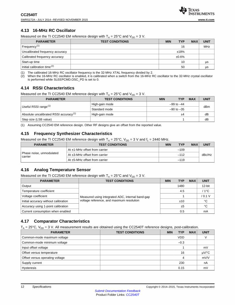
4.13 16-MHz RC OscillatorMeasured on the TI CC2540 EM reference design with TA = 25°C and VDD = 3 V.
PARAMETER TEST CONDITIONS MIN TYP MAX UNITFrequency (1) 16 MHzUncalibrated frequency accuracy ±18%Calibrated frequency accuracy ±0.6%Start-up time 10 µsInitial calibration time (2) 50 µs
(1) The calibrated 16-MHz RC oscillator frequency is the 32-MHz XTAL frequency divided by 2.(2) When the 16-MHz RC oscillator is enabled, it is calibrated when a switch from the 16-MHz RC oscillator to the 32-MHz crystal oscillator
is performed while SLEEPCMD.OSC_PD is set to 0.
4.14 RSSI CharacteristicsMeasured on the TI CC2540 EM reference design with TA = 25°C and VDD = 3 V.
PARAMETER TEST CONDITIONS MIN TYP MAX UNITHigh-gain mode –99 to –44
Useful RSSI range (1) dBmStandard mode –90 to –35
Absolute uncalibrated RSSI accuracy (1) High-gain mode ±4 dBStep size (LSB value) 1 dB
(1) Assuming CC2540 EM reference design. Other RF designs give an offset from the reported value.
4.15 Frequency Synthesizer CharacteristicsMeasured on the TI CC2540 EM reference design with TA = 25°C, VDD = 3 V and fc = 2440 MHz.
PARAMETER TEST CONDITIONS MIN TYP MAX UNITAt ±1-MHz offset from carrier –109
Phase noise, unmodulated At ±3-MHz offset from carrier –112 dBc/HzcarrierAt ±5-MHz offset from carrier –119
4.16 Analog Temperature SensorMeasured on the TI CC2540 EM reference design with TA = 25°C and VDD = 3 V.
PARAMETER TEST CONDITIONS MIN TYP MAX UNITOutput 1480 12-bitTemperature coefficient 4.5 / 1°CVoltage coefficient 1 / 0.1 VMeasured using integrated ADC, internal band-gap
voltage reference, and maximum resolutionInitial accuracy without calibration ±10 °CAccuracy using 1-point calibration ±5 °CCurrent consumption when enabled 0.5 mA
4.17 Comparator CharacteristicsTA = 25°C, VDD = 3 V. All measurement results are obtained using the CC2540T reference designs, post-calibration.
PARAMETER TEST CONDITIONS MIN TYP MAX UNITCommon-mode maximum voltage VDD VCommon-mode minimum voltage –0.3Input offset voltage 1 mVOffset versus temperature 16 µV/°COffset versus operating voltage 4 mV/VSupply current 230 nAHysteresis 0.15 mV
12 Specifications Copyright © 2014–2015, Texas Instruments IncorporatedSubmit Documentation FeedbackProduct Folder Links: CC2540T
CC2540Twww.ti.com SWRS172A –JULY 2014–REVISED NOVEMBER 2015
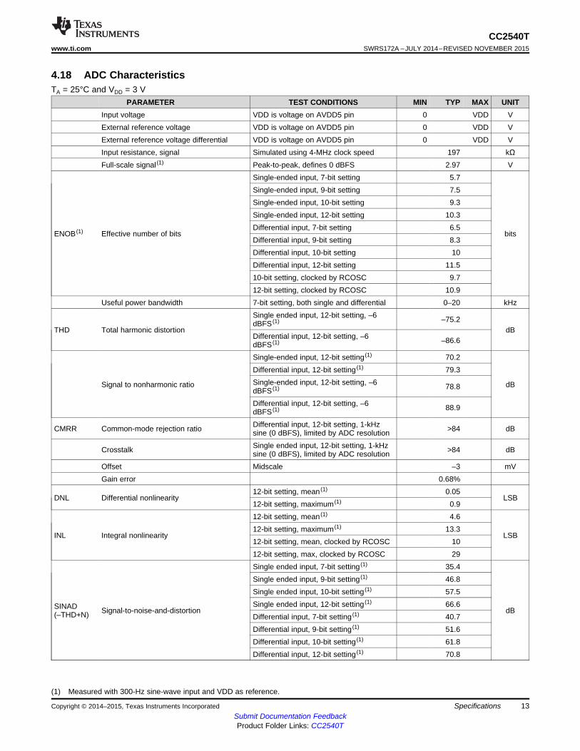
4.18 ADC CharacteristicsTA = 25°C and VDD = 3 V
PARAMETER TEST CONDITIONS MIN TYP MAX UNITInput voltage VDD is voltage on AVDD5 pin 0 VDD VExternal reference voltage VDD is voltage on AVDD5 pin 0 VDD VExternal reference voltage differential VDD is voltage on AVDD5 pin 0 VDD VInput resistance, signal Simulated using 4-MHz clock speed 197 kΩFull-scale signal (1) Peak-to-peak, defines 0 dBFS 2.97 V
Single-ended input, 7-bit setting 5.7Single-ended input, 9-bit setting 7.5Single-ended input, 10-bit setting 9.3Single-ended input, 12-bit setting 10.3Differential input, 7-bit setting 6.5
ENOB (1) Effective number of bits bitsDifferential input, 9-bit setting 8.3Differential input, 10-bit setting 10Differential input, 12-bit setting 11.510-bit setting, clocked by RCOSC 9.712-bit setting, clocked by RCOSC 10.9
Useful power bandwidth 7-bit setting, both single and differential 0–20 kHzSingle ended input, 12-bit setting, –6 –75.2dBFS (1)
THD Total harmonic distortion dBDifferential input, 12-bit setting, –6 –86.6dBFS (1)
Single-ended input, 12-bit setting (1) 70.2Differential input, 12-bit setting (1) 79.3Single-ended input, 12-bit setting, –6Signal to nonharmonic ratio dB78.8dBFS (1)
Differential input, 12-bit setting, –6 88.9dBFS (1)
Differential input, 12-bit setting, 1-kHzCMRR Common-mode rejection ratio >84 dBsine (0 dBFS), limited by ADC resolutionSingle ended input, 12-bit setting, 1-kHzCrosstalk >84 dBsine (0 dBFS), limited by ADC resolution
Offset Midscale –3 mVGain error 0.68%
12-bit setting, mean (1) 0.05DNL Differential nonlinearity LSB
12-bit setting, maximum (1) 0.912-bit setting, mean (1) 4.612-bit setting, maximum (1) 13.3
INL Integral nonlinearity LSB12-bit setting, mean, clocked by RCOSC 1012-bit setting, max, clocked by RCOSC 29Single ended input, 7-bit setting (1) 35.4Single ended input, 9-bit setting (1) 46.8Single ended input, 10-bit setting (1) 57.5Single ended input, 12-bit setting (1) 66.6SINAD Signal-to-noise-and-distortion dB(–THD+N) Differential input, 7-bit setting (1) 40.7Differential input, 9-bit setting (1) 51.6Differential input, 10-bit setting (1) 61.8Differential input, 12-bit setting (1) 70.8
(1) Measured with 300-Hz sine-wave input and VDD as reference.
Copyright © 2014–2015, Texas Instruments Incorporated Specifications 13Submit Documentation FeedbackProduct Folder Links: CC2540T
RESET_N
Px.n
T0299-01
1 2
CC2540TSWRS172A –JULY 2014–REVISED NOVEMBER 2015 www.ti.com
ADC Characteristics (continued)TA = 25°C and VDD = 3 V
PARAMETER TEST CONDITIONS MIN TYP MAX UNIT7-bit setting 209-bit setting 36
Conversion time µs10-bit setting 6812-bit setting 132
Power consumption 1.2 mAInternal reference VDD coefficient 4 mV/VInternal reference temperature coefficient 0.4 mV/10°CInternal reference voltage 1.24 V
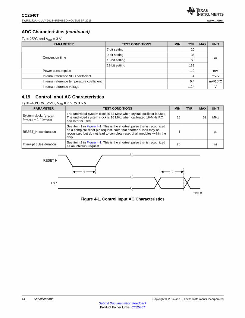
4.19 Control Input AC CharacteristicsTA = –40°C to 125°C, VDD = 2 V to 3.6 V
PARAMETER TEST CONDITIONS MIN TYP MAX UNITThe undivided system clock is 32 MHz when crystal oscillator is used.System clock, fSYSCLK The undivided system clock is 16 MHz when calibrated 16-MHz RC 16 32 MHztSYSCLK = 1 / fSYSCLK oscillator is used.See item 1 in Figure 4-1. This is the shortest pulse that is recognizedas a complete reset pin request. Note that shorter pulses may beRESET_N low duration 1 µsrecognized but do not lead to complete reset of all modules within thechip.See item 2 in Figure 4-1. This is the shortest pulse that is recognizedInterrupt pulse duration 20 nsas an interrupt request.
Figure 4-1. Control Input AC Characteristics
14 Specifications Copyright © 2014–2015, Texas Instruments IncorporatedSubmit Documentation FeedbackProduct Folder Links: CC2540T
T0479-01
SCK
SSN
MOSI
MISO D0 D1X
D0X
t2
t3
X
t8
t10
t11
t9
SCK
SSN
MOSI
MISO
D0 D1X
D0X
t2
t4
t6
t7
t5
t3
X
T0478-01
CC2540Twww.ti.com SWRS172A –JULY 2014–REVISED NOVEMBER 2015
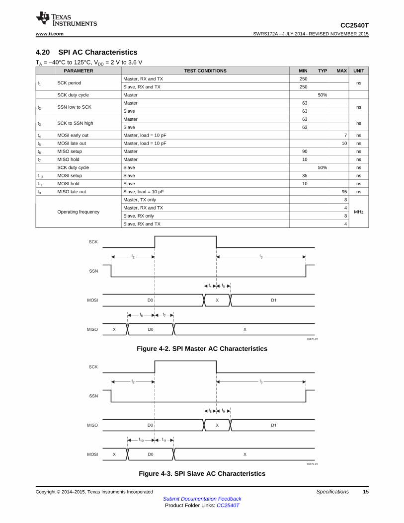
4.20 SPI AC CharacteristicsTA = –40°C to 125°C, VDD = 2 V to 3.6 V
PARAMETER TEST CONDITIONS MIN TYP MAX UNIT
Master, RX and TX 250t1 SCK period ns
Slave, RX and TX 250
SCK duty cycle Master 50%
Master 63t2 SSN low to SCK ns
Slave 63
Master 63t3 SCK to SSN high ns
Slave 63
t4 MOSI early out Master, load = 10 pF 7 ns
t5 MOSI late out Master, load = 10 pF 10 ns
t6 MISO setup Master 90 ns
t7 MISO hold Master 10 ns
SCK duty cycle Slave 50% ns
t10 MOSI setup Slave 35 ns
t11 MOSI hold Slave 10 ns
t9 MISO late out Slave, load = 10 pF 95 ns
Master, TX only 8
Master, RX and TX 4Operating frequency MHz
Slave, RX only 8
Slave, RX and TX 4
Figure 4-2. SPI Master AC Characteristics
Figure 4-3. SPI Slave AC Characteristics
Copyright © 2014–2015, Texas Instruments Incorporated Specifications 15Submit Documentation FeedbackProduct Folder Links: CC2540T
RESET_N
Time
DEBUG_CLKP2_2
t3 t4 t5
T0437-01
Time
DEBUG_CLKP2_2
t1 t2
1/fclk_dbg
T0436-01
CC2540TSWRS172A –JULY 2014–REVISED NOVEMBER 2015 www.ti.com
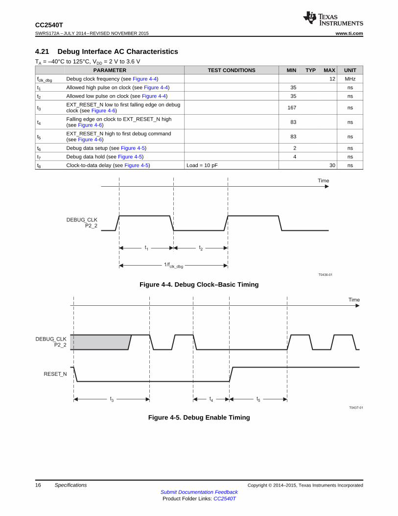
4.21 Debug Interface AC CharacteristicsTA = –40°C to 125°C, VDD = 2 V to 3.6 V
PARAMETER TEST CONDITIONS MIN TYP MAX UNITfclk_dbg Debug clock frequency (see Figure 4-4) 12 MHzt1 Allowed high pulse on clock (see Figure 4-4) 35 nst2 Allowed low pulse on clock (see Figure 4-4) 35 ns
EXT_RESET_N low to first falling edge on debugt3 167 nsclock (see Figure 4-6)Falling edge on clock to EXT_RESET_N hight4 83 ns(see Figure 4-6)EXT_RESET_N high to first debug commandt5 83 ns(see Figure 4-6)
t6 Debug data setup (see Figure 4-5) 2 nst7 Debug data hold (see Figure 4-5) 4 nst8 Clock-to-data delay (see Figure 4-5) Load = 10 pF 30 ns
Figure 4-4. Debug Clock–Basic Timing
Figure 4-5. Debug Enable Timing
16 Specifications Copyright © 2014–2015, Texas Instruments IncorporatedSubmit Documentation FeedbackProduct Folder Links: CC2540T
Time
DEBUG_CLKP2_2
DEBUG_DATA(to CC2540)
P2_1
DEBUG_DATA(from CC2540)
P2_1
T0438-02
t6 t8t7
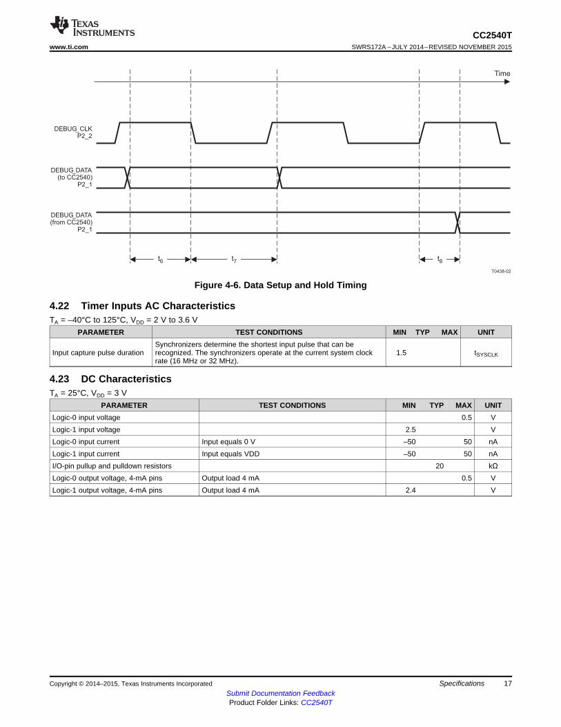
CC2540Twww.ti.com SWRS172A –JULY 2014–REVISED NOVEMBER 2015
Figure 4-6. Data Setup and Hold Timing
4.22 Timer Inputs AC CharacteristicsTA = –40°C to 125°C, VDD = 2 V to 3.6 V
PARAMETER TEST CONDITIONS MIN TYP MAX UNITSynchronizers determine the shortest input pulse that can be
Input capture pulse duration recognized. The synchronizers operate at the current system clock 1.5 tSYSCLKrate (16 MHz or 32 MHz).
4.23 DC CharacteristicsTA = 25°C, VDD = 3 V
PARAMETER TEST CONDITIONS MIN TYP MAX UNITLogic-0 input voltage 0.5 VLogic-1 input voltage 2.5 VLogic-0 input current Input equals 0 V –50 50 nALogic-1 input current Input equals VDD –50 50 nAI/O-pin pullup and pulldown resistors 20 kΩLogic-0 output voltage, 4-mA pins Output load 4 mA 0.5 VLogic-1 output voltage, 4-mA pins Output load 4 mA 2.4 V
Copyright © 2014–2015, Texas Instruments Incorporated Specifications 17Submit Documentation FeedbackProduct Folder Links: CC2540T
Supply Voltage (V)
Cur
rent
(m
A)
2 2.2 2.4 2.6 2.8 3 3.2 3.4 3.619.5
19.52
19.54
19.56
19.58
19.6
19.62
19.64
19.66
19.68
19.7
Supply Voltage (V)
Cur
rent
(m
A)
2 2.2 2.4 2.6 2.8 3 3.2 3.4 3.631
31.1
31.2
31.3
31.4
31.5
31.6
31.7
31.8
31.9
32
Temperature (qC)
Leve
l (dB
m)
-40 -20 0 20 40 60 80 100 120-92
-90
-88
-86
-84
-82
-80
-78
-76
-74
-72
Temperature (qC)
Leve
l (dB
m)
-40 -20 0 20 40 60 80 100 120-2
-1
0
1
2
3
4
5
6
7
Temperature (qC)
Cur
rent
(m
A)
-40 -20 0 20 40 60 80 100 12018
18.5
19
19.5
20
20.5
21
Temperature (qC)
Cur
rent
(m
A)
-40 -20 0 20 40 60 80 100 12030
30.5
31
31.5
32
32.5
33
CC2540TSWRS172A –JULY 2014–REVISED NOVEMBER 2015 www.ti.com
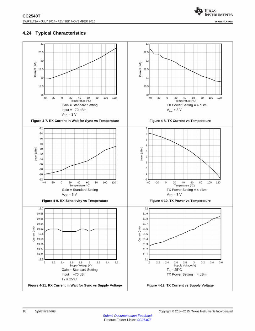
4.24 Typical Characteristics
Gain = Standard Setting TX Power Setting = 4 dBmInput = –70 dBm VCC = 3 VVCC = 3 V
Figure 4-7. RX Current in Wait for Sync vs Temperature Figure 4-8. TX Current vs Temperature
Gain = Standard Setting TX Power Setting = 4 dBmVCC = 3 V VCC = 3 V
Figure 4-9. RX Sensitivity vs Temperature Figure 4-10. TX Power vs Temperature
Gain = Standard Setting TA = 25°CInput = –70 dBm TX Power Setting = 4 dBmTA = 25°C
Figure 4-11. RX Current in Wait for Sync vs Supply Voltage Figure 4-12. TX Current vs Supply Voltage
18 Specifications Copyright © 2014–2015, Texas Instruments IncorporatedSubmit Documentation FeedbackProduct Folder Links: CC2540T
Frequency (MHz)
Leve
l (dB
m)
2400 2420 2440 2460 24803
3.2
3.4
3.6
3.8
4
4.2
4.4
4.6
4.8
5
Frequency (MHz)
Leve
l (dB
m)
2400 2420 2440 2460 2480-89
-88.8
-88.6
-88.4
-88.2
-88
-87.8
-87.6
-87.4
-87.2
-87
Frequency (MHz)
Rej
ectio
n (d
B)
2400 2420 2440 2460 2480-10
0
10
20
30
40
50
60
70
Supply Voltage (V)
Leve
l (dB
m)
2 2.2 2.4 2.6 2.8 3 3.2 3.4 3.6-89
-88.8
-88.6
-88.4
-88.2
-88
-87.8
-87.6
-87.4
-87.2
-87
Supply Voltage (V)
Leve
l (dB
m)
2 2.2 2.4 2.6 2.8 3 3.2 3.4 3.63
3.2
3.4
3.6
3.8
4
4.2
4.4
4.6
4.8
5
CC2540Twww.ti.com SWRS172A –JULY 2014–REVISED NOVEMBER 2015
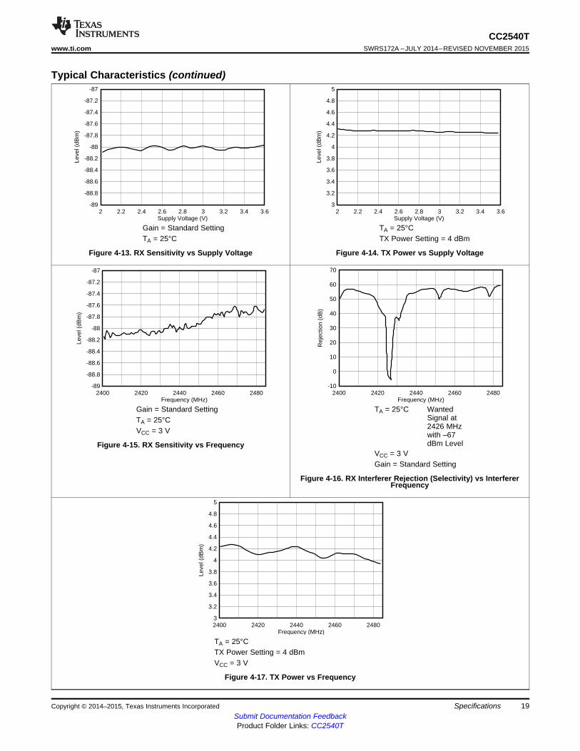
Typical Characteristics (continued)
Gain = Standard Setting TA = 25°CTA = 25°C TX Power Setting = 4 dBm
Figure 4-13. RX Sensitivity vs Supply Voltage Figure 4-14. TX Power vs Supply Voltage
Gain = Standard Setting TA = 25°C WantedSignal atTA = 25°C2426 MHzVCC = 3 V with –67dBm LevelFigure 4-15. RX Sensitivity vs Frequency
VCC = 3 VGain = Standard Setting
Figure 4-16. RX Interferer Rejection (Selectivity) vs InterfererFrequency
TA = 25°CTX Power Setting = 4 dBmVCC = 3 V
Figure 4-17. TX Power vs Frequency
Copyright © 2014–2015, Texas Instruments Incorporated Specifications 19Submit Documentation FeedbackProduct Folder Links: CC2540T
CC2540 Current ConsumptionRX SG CLKCONMOD0x80
0
5
10
15
20
25
2.1 2.4 2.7 3 3.3 3.6
Supply (V)
Cu
rren
t(m
A)
0
5
10
15
20
25
30
35
40
Cu
rren
tS
avin
gs
(%)
DC/DC ON
DC/DC OFF
Current Savings
CC2540 Current ConsumptionTX 4dBm
0
5
10
15
20
25
30
35
2.1 2.4 2.7 3 3.3 3.6
Supply (V)
Cu
rren
t(m
A)
0
5
10
15
20
25
30
35
40
Cu
rren
tS
avin
gs
(%)
DC/DC ON
DC/DC OFF
% Current Savings
CC2540TSWRS172A –JULY 2014–REVISED NOVEMBER 2015 www.ti.com
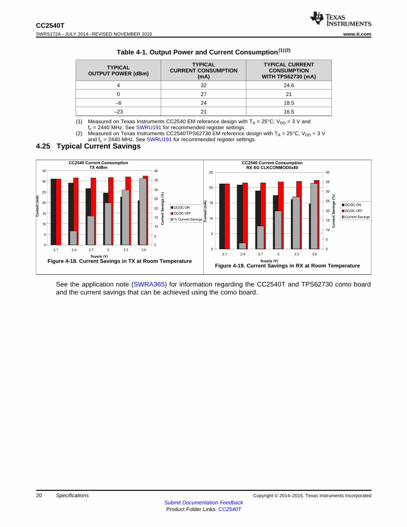
Table 4-1. Output Power and Current Consumption (1) (2)
TYPICAL TYPICAL CURRENTTYPICAL CURRENT CONSUMPTION CONSUMPTIONOUTPUT POWER (dBm) (mA) WITH TPS62730 (mA)4 32 24.60 27 21–6 24 18.5–23 21 16.5
(1) Measured on Texas Instruments CC2540 EM reference design with TA = 25°C, VDD = 3 V andfc = 2440 MHz. See SWRU191 for recommended register settings.
(2) Measured on Texas Instruments CC2540TPS62730 EM reference design with TA = 25°C, VDD = 3 Vand fc = 2440 MHz. See SWRU191 for recommended register settings.
4.25 Typical Current Savings
Figure 4-18. Current Savings in TX at Room TemperatureFigure 4-19. Current Savings in RX at Room Temperature
See the application note (SWRA365) for information regarding the CC2540T and TPS62730 como boardand the current savings that can be achieved using the como board.
20 Specifications Copyright © 2014–2015, Texas Instruments IncorporatedSubmit Documentation FeedbackProduct Folder Links: CC2540T
CC2540Twww.ti.com SWRS172A –JULY 2014–REVISED NOVEMBER 2015
5 Detailed Description
5.1 OverviewThe modules of the CC2540T device can be roughly divided into one of three categories:• CPU-related modules• Modules related to power, test, and clock distribution• Radio-related modules
A short description of each module is given in the following subsections.
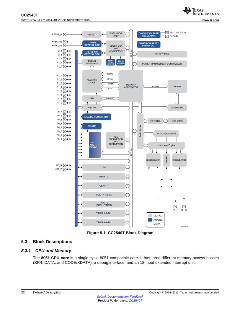
5.2 Functional Block DiagramA block diagram of the CC2540T is shown in Figure 5-1.
Copyright © 2014–2015, Texas Instruments Incorporated Detailed Description 21Submit Documentation FeedbackProduct Folder Links: CC2540T
RESETWATCHDOG
TIMER
IRQ CTRL FLASH CTRL
DEBUGINTERFACE
CLOCK MUXand
CALIBRATION
DMA
8051 CPUCORE
32-MHz
CRYSTAL OSC
OP-AMP
32.768-kHz
CRYSTAL OSC
HIGH-
SPEED
RC-OSC POWER MANAGEMENT CONTROLLER
USART 0
USB
USART 1
TIMER 1 (16-Bit)
TIMER 3 (8-Bit)
TIMER 4 (8-Bit)
TIMER 2(BLE LL TIMER)
FLASH
FIFOCTRL 1 KB SRAM
ON-CHIP VOLTAGE
REGULATOR
POWER-ON RESET
BROWN OUT
VDD (2 V–3.6 V)
DCOUPLRESET_N
XOSC_Q2
XOSC_Q1
P2_4
P1_7
P0_7
P2_3
P1_6
P0_6
P2_2
P1_5
P0_5
P1_2
P0_2
P2_1
P1_4
P0_4
P1_1
P0_1
P2_0
P1_3
P0_3
P1_0
P0_0
MODULATORDEMODULATOR
RECEIVE TRANSMIT
FR
EQ
UE
NC
Y
SY
NT
HE
SIZ
ER
SY
NT
H
RF_P RF_N
B0301-05
RADIO REGISTERS
SF
R B
us
SF
R B
us
DS
ADC
AUDIO/DC
AESENCRYPTION
ANDDECRYPTION
MEMORYARBITRATOR FLASH
UNIFIED
SFR
IRAM
XRAM
PDATA
SLEEP TIMER
32-kHz
RC-OSC
I/O
CO
NT
RO
LL
ER
DIGITAL
ANALOG
MIXED
ANALOG COMPARATOR
USB_N
USB_P
Ra
dio
Arb
ite
r
Link Layer Engine
CC2540TSWRS172A –JULY 2014–REVISED NOVEMBER 2015 www.ti.com
Figure 5-1. CC2540T Block Diagram
5.3 Block Descriptions
5.3.1 CPU and MemoryThe 8051 CPU core is a single-cycle 8051-compatible core. It has three different memory access busses(SFR, DATA, and CODE/XDATA), a debug interface, and an 18-input extended interrupt unit.
22 Detailed Description Copyright © 2014–2015, Texas Instruments IncorporatedSubmit Documentation FeedbackProduct Folder Links: CC2540T
CC2540Twww.ti.com SWRS172A –JULY 2014–REVISED NOVEMBER 2015
The memory arbiter is at the heart of the system, as it connects the CPU and DMA controller with thephysical memories and all peripherals through the SFR bus. The memory arbiter has four memory-accesspoints, access of which can map to one of three physical memories: an SRAM, flash memory, withXREG/SFR registers. It is responsible for performing arbitration and sequencing between simultaneousmemory accesses to the same physical memory.
The SFR bus is drawn conceptually in Figure 5-1 as a common bus that connects all hardwareperipherals to the memory arbiter. The SFR bus in the block diagram also provides access to the radioregisters in the radio register bank, even though these are indeed mapped into XDATA memory space.
The 8-KB SRAM maps to the DATA memory space and to parts of the XDATA memory spaces. TheSRAM is an ultralow-power SRAM that retains its contents even when the digital part is powered off(power modes 2 and 3).
The 256-KB flash block provides in-circuit programmable non-volatile program memory for the device,and maps into the CODE and XDATA memory spaces.
5.3.2 PeripheralsWriting to the flash block is performed through a flash controller that allows page-wise erasure and4-bytewise programming. See the User's Guide (SWRU191) for details on the flash controller.
A versatile five-channel DMA controller is available in the system, accesses memory using the XDATAmemory space, and thus has access to all physical memories. Each channel (trigger, priority, transfermode, addressing mode, source and destination pointers, and transfer count) is configured with DMAdescriptors that can be located anywhere in memory. Many of the hardware peripherals (AES core, flashcontroller, USARTs, timers, ADC interface, and so forth) can be used with the DMA controller for efficientoperation by performing data transfers between a single SFR or XREG address and flash/SRAM.
Each CC2540T contains a unique 48-bit IEEE address that can be used as the public device address for aBluetooth device. Designers are free to use this address, or provide their own, as described in theBluetooth specification.
The interrupt controller services a total of 18 interrupt sources, divided into six interrupt groups, each ofwhich is associated with one of four interrupt priorities. I/O and sleep timer interrupt requests are servicedeven if the device is in a sleep mode (power modes 1 and 2) by bringing the CC2540T back to the activemode.
The debug interface implements a proprietary two-wire serial interface that is used for in-circuitdebugging. Through this debug interface, it is possible to erase or program the entire flash memory,control which oscillators are enabled, stop and start execution of the user program, execute instructionson the 8051 core, set code breakpoints, and single-step through instructions in the code. Using thesetechniques, it is possible to perform in-circuit debugging and external flash programming elegantly.
The I/O controller is responsible for all general-purpose I/O pins. The CPU can configure whetherperipheral modules control certain pins or whether they are under software control, and if so, whethereach pin is configured as an input or output and if a pullup or pulldown resistor in the pad is connected.Each peripheral that connects to the I/O pins can choose between two different I/O pin locations to ensureflexibility in various applications.
The sleep timer is an ultralow-power timer that can either use an external 32.768-kHz crystal oscillator oran internal 32.753-kHz RC oscillator. The sleep timer runs continuously in all operating modes exceptpower mode 3. Typical applications of this timer are as a real-time counter or as a wake-up timer to getout of power modes 1 or 2.
A built-in watchdog timer allows the CC2540T to reset itself if the firmware hangs. When enabled bysoftware, the watchdog timer must be cleared periodically; otherwise, it resets the device when it timesout.
Copyright © 2014–2015, Texas Instruments Incorporated Detailed Description 23Submit Documentation FeedbackProduct Folder Links: CC2540T
CC2540TSWRS172A –JULY 2014–REVISED NOVEMBER 2015 www.ti.com
Timer 1 is a 16-bit timer with timer/counter/PWM functionality. It has a programmable prescaler, a 16-bitperiod value, and five individually programmable counter/capture channels, each with a 16-bit comparevalue. Each of the counter and capture channels can be used as a PWM output or to capture the timing ofedges on input signals. It can also be configured in IR generation mode, where it counts timer 3 periodsand the output is ANDed with the output of timer 3 to generate modulated consumer IR signals withminimal CPU interaction.
Timer 2 is a 40-bit timer used by the Bluetooth low energy stack. It has a 16-bit counter with aconfigurable timer period and a 24-bit overflow counter that can be used to keep track of the number ofperiods that have transpired. A 40-bit capture register is also used to record the exact time at which astart-of-frame delimiter is received or transmitted, or it is used to record the exact time at whichtransmission ends. There are two 16-bit timer-compare registers and two 24-bit overflow-compareregisters that can be used to give exact timing for the start of RX or TX to the radio or general interrupts.
Timer 3 and timer 4 are 8-bit timers with timer/counter/PWM functionality. They have a programmableprescaler, an 8-bit period value, and one programmable counter channel with an 8-bit compare value.Each of the counter channels can be used as PWM output.
USART 0 and USART 1 are each configurable as either an SPI master or slave, or as a UART. Theyprovide double buffering on both RX and TX and hardware flow control and are thus well suited to high-throughput full-duplex applications. Each USART has its own high-precision baud-rate generator, whichleaves the ordinary timers free for other uses. When configured as SPI slaves, the USARTs sample theinput signal using SCK directly instead of using some oversampling scheme, and are thus well-suited forhigh data rates.
The AES encryption/decryption core allows the user to encrypt and decrypt data using the AESalgorithm with 128-bit keys. The AES core also supports ECB, CBC, CFB, OFB, CTR, and CBC-MAC, aswell as hardware support for CCM.
The ADC supports 7 to 12 bits of resolution with a corresponding range of bandwidths from 30-kHz to4-kHz, respectively. DC and audio conversions with up to eight input channels (I/O controller pins) arepossible. The inputs can be selected as single-ended or differential. The reference voltage can be internal,AVDD, or a single-ended or differential external signal. The ADC also has a temperature-sensor inputchannel. The ADC can automate the process of periodic sampling or conversion over a sequence ofchannels.
The ultralow-power analog comparator enables applications to wake up from PM2 or PM3 based on ananalog signal. Both inputs are brought out to pins; the reference voltage must be provided externally. Thecomparator output is connected to the I/O controller interrupt detector and can be treated by the MCU as aregular I/O pin interrupt.
24 Detailed Description Copyright © 2014–2015, Texas Instruments IncorporatedSubmit Documentation FeedbackProduct Folder Links: CC2540T
DGND_USB
USB_P
USB_N
DVDD_USB
P1_5
DVDD2
P1_1
P1_2
P1_3
P1_4
2-V to 3.6-V Power Supply
R301
C251
C261
C262 C253
C252
L251
L261
L252 L253
XTAL1
C221 C231
XTA
L2
C321
C331
C401
32-kHz Crystal(1)
CC2540T
DIE ATTACH PAD
RBIAS
AVDD4
AVDD1
AVDD2
RF_N
AVDD5
XOSC_Q1
XOSC_Q2
AVDD3
RF_P
P1
_0
P0
_7
P0
_6
P0
_5
P0
_4
RE
SE
T_
N
P0
_0
P0
_1
P0
_2
P0
_3
DC
OU
PL
DV
DD
1
P1_
6
P1_
7
P2_
0
AV
DD
6
P2
_4
/XO
SC
32K
_Q
1
P2
_3
/XO
SC
32K
_Q
2
P2_
2
P2_
1
Antenna
(50 )W
S0383-03
1
2
3
4
5
6
7
8
9
10
11
12
13
14
15
16
17
18
19
20
21
22
23
24
25
26
27
28
29
30
31
32
33
34
35
36
37
38
39
40
Power Supply Decoupling Capacitors are Not ShownDigital I/O Not Connected
CC2540Twww.ti.com SWRS172A –JULY 2014–REVISED NOVEMBER 2015
6 Applications, Implementation, and Layout
NOTEInformation in the following Applications section is not part of the TI component specification,and TI does not warrant its accuracy or completeness. TI’s customers are responsible fordetermining suitability of components for their purposes. Customers should validate and testtheir design implementation to confirm system functionality.
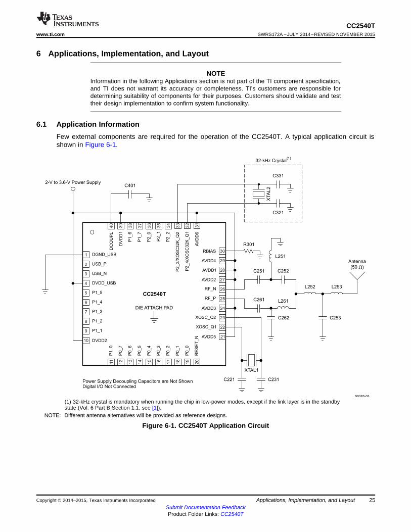
6.1 Application InformationFew external components are required for the operation of the CC2540T. A typical application circuit isshown in Figure 6-1.
(1) 32-kHz crystal is mandatory when running the chip in low-power modes, except if the link layer is in the standbystate (Vol. 6 Part B Section 1.1, see [1]).
NOTE: Different antenna alternatives will be provided as reference designs.
Figure 6-1. CC2540T Application Circuit
Copyright © 2014–2015, Texas Instruments Incorporated Applications, Implementation, and Layout 25Submit Documentation FeedbackProduct Folder Links: CC2540T
L parasitic
321 331
1C C
1 1
C C
= +
+
L parasitic
221 231
1C C
1 1
C C
= +
+
CC2540TSWRS172A –JULY 2014–REVISED NOVEMBER 2015 www.ti.com
Table 6-1. Overview of External Components (Excluding Supply Decoupling Capacitors)
COMPONENT DESCRIPTION VALUEC221 32-MHz XTAL loading capacitor 12 pFC231 32-MHz XTAL loading capacitor 12 pFC251 Part of the RF matching network 18 pFC252 Part of the RF matching network 1 pFC253 Part of the RF matching network 1 pFC261 Part of the RF matching network 18 pFC262 Part of the RF matching network 1 pFC321 32-kHz XTAL loading capacitor 15 pFC331 32-kHz XTAL loading capacitor 15 pFC401 Decoupling capacitor for the internal digital regulator 1 µFL251 Part of the RF matching network 2 nHL252 Part of the RF matching network 1 nHL253 Part of the RF matching network 3 nHL261 Part of the RF matching network 2 nHR301 Resistor used for internal biasing 56 kΩ
6.2 Input/Output MatchingWhen using an unbalanced antenna such as a monopole, a balun should be used to optimizeperformance. The balun can be implemented using low-cost discrete inductors and capacitors. Therecommended balun shown consists of C262, L261, C252, and L252.
6.3 CrystalAn external 32-MHz crystal, XTAL1, with two loading capacitors (C221 and C231) is used for the 32-MHzcrystal oscillator. See Section 4.10 for details. The load capacitance seen by the 32-MHz crystal is givenby Equation 1:
(1)
XTAL2 is an optional 32.768-kHz crystal, with two loading capacitors (C321 and C331) used for the32.768-kHz crystal oscillator. The 32.768-kHz crystal oscillator is used in applications where both very lowsleep-current consumption and accurate wake-up times are needed. The load capacitance seen by the32.768-kHz crystal is given by Equation 2:
(2)
A series resistor may be used to comply with the ESR requirement.
6.4 On-Chip 1.8-V Voltage Regulator DecouplingThe 1.8-V on-chip voltage regulator supplies the 1.8-V digital logic. This regulator requires a decouplingcapacitor (C401) for stable operation.
6.5 Power-Supply Decoupling and FilteringProper power-supply decoupling must be used for optimum performance. The placement and size of thedecoupling capacitors and the power supply filtering are very important to achieve the best performance inan application. TI provides a compact reference design that should be followed very closely (seeSection 6.6).
26 Applications, Implementation, and Layout Copyright © 2014–2015, Texas Instruments IncorporatedSubmit Documentation FeedbackProduct Folder Links: CC2540T
CC2540Twww.ti.com SWRS172A –JULY 2014–REVISED NOVEMBER 2015
6.6 Reference DesignBluetooth Low Energy Light Reference Design
This reference design is an example of using the SimpleLink™ Bluetooth low energy CC2540T hightemperature range, wireless microcontroller in lighting applications. The board includes RGBW LEDscontrolled by the CC2540T and is USB powered. The board can be controlled out-of-the-box by the TIBLE Multitool smart phone app.
Copyright © 2014–2015, Texas Instruments Incorporated Applications, Implementation, and Layout 27Submit Documentation FeedbackProduct Folder Links: CC2540T
CC2540TSWRS172A –JULY 2014–REVISED NOVEMBER 2015 www.ti.com
7 Device and Documentation Support
7.1 Documentation Support
7.1.1 Related DocumentationThe following documents describe the CC2540T processor. Copies of these documents are available onthe Internet at www.ti.com.
[1] Bluetooth® Core Technical Specification, Core Version 4.0
SWRU191 CC253x System-on-Chip Solution for 2.4-GHz IEEE 802.15.4 and ZigBee® Applications,CC2540/41 System-on-Chip Solution for 2.4-GHz Bluetooth Low Energy Applications
SWRA365 Current Savings in CC254x Using the TPS62730
7.1.2 Community ResourcesThe following links connect to TI community resources. Linked contents are provided "AS IS" by therespective contributors. They do not constitute TI specifications and do not necessarily reflect TI's views;see TI's Terms of Use.
TI E2E™ Online Community TI's Engineer-to-Engineer (E2E) Community. Created to fostercollaboration among engineers. At e2e.ti.com, you can ask questions, share knowledge,explore ideas and help solve problems with fellow engineers.
TI Embedded Processors Wiki Texas Instruments Embedded Processors Wiki. Established to helpdevelopers get started with Embedded Processors from Texas Instruments and to fosterinnovation and growth of general knowledge about the hardware and software surroundingthese devices.
7.2 Texas Instruments Low-Power RF Website• Forums, videos, and blogs• RF design help• E2E interaction
Join us today at www.ti.com/lprf-forum.
7.3 Texas Instruments Low-Power RF Developer NetworkTexas Instruments has launched an extensive network of low-power RF development partners to helpcustomers speed up their application development. The network consists of recommended companies, RFconsultants, and independent design houses that provide a series of hardware module products anddesign services, including:• RF circuit, low-power RF, and ZigBee® design services• Low-power RF and ZigBee module solutions and development tools• RF certification services and RF circuit manufacturing
Need help with modules, engineering services, or development tools?
Search the Low-Power RF Developer Network tool to find a suitable partner.www.ti.com/lprfnetwork
28 Device and Documentation Support Copyright © 2014–2015, Texas Instruments IncorporatedSubmit Documentation FeedbackProduct Folder Links: CC2540T
CC2540Twww.ti.com SWRS172A –JULY 2014–REVISED NOVEMBER 2015
7.4 Low-Power RF eNewsletterThe Low-Power RF eNewsletter keeps the user up-to-date on new products, news releases, developers’news, and other news and events associated with low-power RF products from TI. The Low-Power RFeNewsletter articles include links to get more online information.
Sign up today onwww.ti.com/lprfnewsletter
7.5 TrademarksSmartRF, SimpleLink, E2E are trademarks of Texas Instruments.Bluetooth is a registered trademark of Bluetooth SIG, Inc.IAR Embedded Workbench is a trademark of IAR Systems AB.ZigBee is a registered trademark of ZigBee Alliance, Inc.All other trademarks are the property of their respective owners.
7.6 Electrostatic Discharge CautionThis integrated circuit can be damaged by ESD. Texas Instruments recommends that all integrated circuits be handled withappropriate precautions. Failure to observe proper handling and installation procedures can cause damage.
ESD damage can range from subtle performance degradation to complete device failure. Precision integrated circuits may be moresusceptible to damage because very small parametric changes could cause the device not to meet its published specifications.
7.7 Export Control NoticeRecipient agrees to not knowingly export or re-export, directly or indirectly, any product or technical data(as defined by the U.S., EU, and other Export Administration Regulations) including software, or anycontrolled product restricted by other applicable national regulations, received from disclosing party undernondisclosure obligations (if any), or any direct product of such technology, to any destination to whichsuch export or re-export is restricted or prohibited by U.S. or other applicable laws, without obtaining priorauthorization from U.S. Department of Commerce and other competent Government authorities to theextent required by those laws.
7.8 GlossaryTI Glossary This glossary lists and explains terms, acronyms, and definitions.
8 Mechanical Packaging and Orderable Information
8.1 Packaging InformationThe following pages include mechanical packaging and orderable information. This information is the mostcurrent data available for the designated devices. This data is subject to change without notice andrevision of this document. For browser-based versions of this data sheet, refer to the left-hand navigation.
Copyright © 2014–2015, Texas Instruments Incorporated Mechanical Packaging and Orderable Information 29Submit Documentation FeedbackProduct Folder Links: CC2540T
PACKAGE OPTION ADDENDUM
www.ti.com 11-Dec-2020
Addendum-Page 1
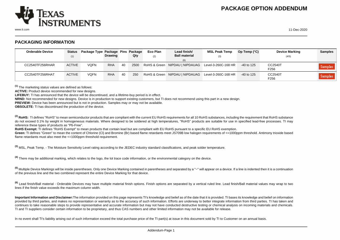
PACKAGING INFORMATION
Orderable Device Status(1)
Package Type PackageDrawing
Pins PackageQty
Eco Plan(2)
Lead finish/Ball material
(6)
MSL Peak Temp(3)
Op Temp (°C) Device Marking(4/5)
Samples
CC2540TF256RHAR ACTIVE VQFN RHA 40 2500 RoHS & Green NIPDAU | NIPDAUAG Level-3-260C-168 HR -40 to 125 CC2540TF256
CC2540TF256RHAT ACTIVE VQFN RHA 40 250 RoHS & Green NIPDAU | NIPDAUAG Level-3-260C-168 HR -40 to 125 CC2540TF256
(1) The marketing status values are defined as follows:ACTIVE: Product device recommended for new designs.LIFEBUY: TI has announced that the device will be discontinued, and a lifetime-buy period is in effect.NRND: Not recommended for new designs. Device is in production to support existing customers, but TI does not recommend using this part in a new design.PREVIEW: Device has been announced but is not in production. Samples may or may not be available.OBSOLETE: TI has discontinued the production of the device.
(2) RoHS: TI defines "RoHS" to mean semiconductor products that are compliant with the current EU RoHS requirements for all 10 RoHS substances, including the requirement that RoHS substancedo not exceed 0.1% by weight in homogeneous materials. Where designed to be soldered at high temperatures, "RoHS" products are suitable for use in specified lead-free processes. TI mayreference these types of products as "Pb-Free".RoHS Exempt: TI defines "RoHS Exempt" to mean products that contain lead but are compliant with EU RoHS pursuant to a specific EU RoHS exemption.Green: TI defines "Green" to mean the content of Chlorine (Cl) and Bromine (Br) based flame retardants meet JS709B low halogen requirements of <=1000ppm threshold. Antimony trioxide basedflame retardants must also meet the <=1000ppm threshold requirement.
(3) MSL, Peak Temp. - The Moisture Sensitivity Level rating according to the JEDEC industry standard classifications, and peak solder temperature.
(4) There may be additional marking, which relates to the logo, the lot trace code information, or the environmental category on the device.
(5) Multiple Device Markings will be inside parentheses. Only one Device Marking contained in parentheses and separated by a "~" will appear on a device. If a line is indented then it is a continuationof the previous line and the two combined represent the entire Device Marking for that device.
(6) Lead finish/Ball material - Orderable Devices may have multiple material finish options. Finish options are separated by a vertical ruled line. Lead finish/Ball material values may wrap to twolines if the finish value exceeds the maximum column width.
Important Information and Disclaimer:The information provided on this page represents TI's knowledge and belief as of the date that it is provided. TI bases its knowledge and belief on informationprovided by third parties, and makes no representation or warranty as to the accuracy of such information. Efforts are underway to better integrate information from third parties. TI has taken andcontinues to take reasonable steps to provide representative and accurate information but may not have conducted destructive testing or chemical analysis on incoming materials and chemicals.TI and TI suppliers consider certain information to be proprietary, and thus CAS numbers and other limited information may not be available for release.
In no event shall TI's liability arising out of such information exceed the total purchase price of the TI part(s) at issue in this document sold by TI to Customer on an annual basis.
PACKAGE OPTION ADDENDUM
www.ti.com 11-Dec-2020
Addendum-Page 2
www.ti.com
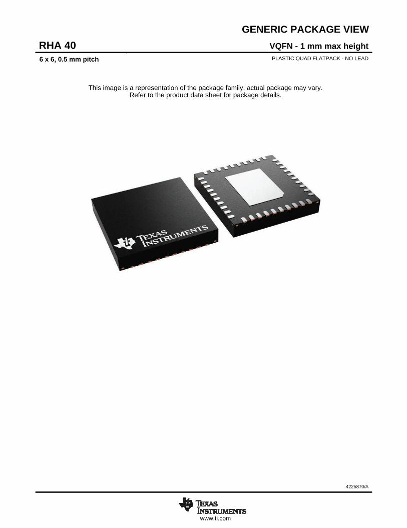
GENERIC PACKAGE VIEW
This image is a representation of the package family, actual package may vary.Refer to the product data sheet for package details.
VQFN - 1 mm max heightRHA 40PLASTIC QUAD FLATPACK - NO LEAD6 x 6, 0.5 mm pitch
4225870/A
www.ti.com
PACKAGE OUTLINE
C
40X 0.30.2
4.5 0.1
40X 0.50.3
1 MAX
(0.2) TYP
0.050.00
36X 0.5
2X4.5
2X 4.5
A 6.15.9
B
6.15.9
0.30.2
0.50.3
(0.1)
VQFN - 1 mm max heightRHA0040HPLASTIC QUAD FLATPACK - NO LEAD
4219055/B 08/22/2019
PIN 1 INDEX AREA
0.08 C
SEATING PLANE
1
10 21
30
11 20
40 31
(OPTIONAL)PIN 1 ID 0.1 C A B
0.05
EXPOSEDTHERMAL PAD
DETAILSEE TERMINAL
SYMM
SYMM
NOTES: 1. All linear dimensions are in millimeters. Any dimensions in parenthesis are for reference only. Dimensioning and tolerancing per ASME Y14.5M. 2. This drawing is subject to change without notice. 3. The package thermal pad must be soldered to the printed circuit board for thermal and mechanical performance.
41
SEE SIDE WALLDETAIL
SCALE 2.200
DETAILOPTIONAL TERMINAL
TYPICAL
SIDE WALL DETAILOPTIONAL METAL THICKNESS
www.ti.com
EXAMPLE BOARD LAYOUT
0.07 MINALL AROUND
0.07 MAXALL AROUND
40X (0.25)
40X (0.6)
( 0.2) TYPVIA
36X (0.5)
(5.8)
(5.8)
( 4.5)
(R0.05)TYP
4X(1.46)
4X(1.27)
(0.73) TYP
4X (1.27)
(0.73)TYP
4X (1.46)
VQFN - 1 mm max heightRHA0040HPLASTIC QUAD FLATPACK - NO LEAD
4219055/B 08/22/2019
SYMM
1
10
11 20
21
30
3140
SYMM
LAND PATTERN EXAMPLEEXPOSED METAL SHOWN
SCALE:12X
41
NOTES: (continued) 4. This package is designed to be soldered to a thermal pad on the board. For more information, see Texas Instruments literature number SLUA271 (www.ti.com/lit/slua271).5. Vias are optional depending on application, refer to device data sheet. If any vias are implemented, refer to their locations shown on this view. It is recommended that vias under paste be filled, plugged or tented.
SOLDER MASKOPENING
METAL UNDERSOLDER MASK
SOLDER MASKDEFINED
EXPOSED METALMETAL
SOLDER MASKOPENING
SOLDER MASK DETAILS
NON SOLDER MASKDEFINED
(PREFERRED)
EXPOSED METAL
www.ti.com
EXAMPLE STENCIL DESIGN
40X (0.6)
40X (0.25)
36X (0.5)
(5.8)
(5.8)
9X ( 1.26)
(1.46)TYP
(1.46) TYP
(R0.05) TYP
VQFN - 1 mm max heightRHA0040HPLASTIC QUAD FLATPACK - NO LEAD
4219055/B 08/22/2019
NOTES: (continued) 6. Laser cutting apertures with trapezoidal walls and rounded corners may offer better paste release. IPC-7525 may have alternate design recommendations.
SYMM
METALTYP
SOLDER PASTE EXAMPLEBASED ON 0.125 mm THICK STENCIL
EXPOSED PAD 41:
70% PRINTED SOLDER COVERAGE BY AREASCALE:15X
SYMM
1
10
11 20
21
30
3140
41
IMPORTANT NOTICE AND DISCLAIMERTI PROVIDES TECHNICAL AND RELIABILITY DATA (INCLUDING DATASHEETS), DESIGN RESOURCES (INCLUDING REFERENCEDESIGNS), APPLICATION OR OTHER DESIGN ADVICE, WEB TOOLS, SAFETY INFORMATION, AND OTHER RESOURCES “AS IS”AND WITH ALL FAULTS, AND DISCLAIMS ALL WARRANTIES, EXPRESS AND IMPLIED, INCLUDING WITHOUT LIMITATION ANYIMPLIED WARRANTIES OF MERCHANTABILITY, FITNESS FOR A PARTICULAR PURPOSE OR NON-INFRINGEMENT OF THIRDPARTY INTELLECTUAL PROPERTY RIGHTS.These resources are intended for skilled developers designing with TI products. You are solely responsible for (1) selecting the appropriateTI products for your application, (2) designing, validating and testing your application, and (3) ensuring your application meets applicablestandards, and any other safety, security, or other requirements. These resources are subject to change without notice. TI grants youpermission to use these resources only for development of an application that uses the TI products described in the resource. Otherreproduction and display of these resources is prohibited. No license is granted to any other TI intellectual property right or to any third partyintellectual property right. TI disclaims responsibility for, and you will fully indemnify TI and its representatives against, any claims, damages,costs, losses, and liabilities arising out of your use of these resources.TI’s products are provided subject to TI’s Terms of Sale (https:www.ti.com/legal/termsofsale.html) or other applicable terms available eitheron ti.com or provided in conjunction with such TI products. TI’s provision of these resources does not expand or otherwise alter TI’sapplicable warranties or warranty disclaimers for TI products.IMPORTANT NOTICE
Mailing Address: Texas Instruments, Post Office Box 655303, Dallas, Texas 75265Copyright © 2021, Texas Instruments Incorporated