Embed Size (px)
Citation preview

CC3100MOD SimpleLink™ Wi-Fi® NetworkProcessor Module - BoosterPack Hardware
User's Guide
Literature Number: SWRU396BDecember 2014–Revised May 2018
2 SWRU396B–December 2014–Revised May 2018Submit Documentation Feedback
Copyright © 2014–2018, Texas Instruments Incorporated
Table of Contents
Contents
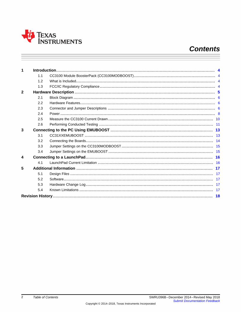
1 Introduction......................................................................................................................... 41.1 CC3100 Module BoosterPack (CC3100MODBOOST).............................................................. 41.2 What is Included.......................................................................................................... 41.3 FCC/IC Regulatory Compliance........................................................................................ 4
2 Hardware Description ........................................................................................................... 52.1 Block Diagram ............................................................................................................ 62.2 Hardware Features....................................................................................................... 62.3 Connector and Jumper Descriptions .................................................................................. 62.4 Power ...................................................................................................................... 82.5 Measure the CC3100 Current Drawn ................................................................................ 102.6 Performing Conducted Testing ....................................................................................... 11
3 Connecting to the PC Using EMUBOOST .............................................................................. 133.1 CC31XXEMUBOOST .................................................................................................. 133.2 Connecting the Boards................................................................................................. 143.3 Jumper Settings on the CC3100MODBOOST...................................................................... 153.4 Jumper Settings on the EMUBOOST ................................................................................ 15
4 Connecting to a LaunchPad................................................................................................. 164.1 LaunchPad Current Limitation ........................................................................................ 16
5 Additional Information ........................................................................................................ 175.1 Design Files ............................................................................................................. 175.2 Software.................................................................................................................. 175.3 Hardware Change Log ................................................................................................. 175.4 Known Limitations ...................................................................................................... 17
Revision History.......................................................................................................................... 18
www.ti.com
3SWRU396B–December 2014–Revised May 2018Submit Documentation Feedback
Copyright © 2014–2018, Texas Instruments Incorporated
List of Figures
List of Figures1 CC3100MOD BoosterPack Board With the CC3100MOD ............................................................. 42 CC3100MODBOOST Front Side .......................................................................................... 53 CC3100MODBOOST Block Diagram ..................................................................................... 64 Signal Assignments.......................................................................................................... 75 3.3-V Power From MCU ................................................................................................... 96 Feed USB on the BoosterPack (if the LaunchPad Cannot Source 5 V on 20-Pin Connector) .................... 97 3.3-V Power From LDO ................................................................................................... 108 Feed USB on the BoosterPack (Always While Using the Onboard LDO) .......................................... 109 Low Current Measurement................................................................................................ 1110 Active Current Measurement ............................................................................................. 1111 Connectors on the Board ................................................................................................. 1212 Resistor Switch for Radiated versus Conducted Tests................................................................ 1213 CC31XXEMUBOOST Board.............................................................................................. 1314 Portable Devices ........................................................................................................... 1415 The CC3100BOOST Connected to the EMUBOOST ................................................................ 1516 CC3100MODBOOST Connected to MSP430F5529 LaunchPad .................................................... 1617 Jumper Settings When Used With LaunchPad ........................................................................ 16
List of Tables1 Push Buttons ................................................................................................................. 62 LEDs........................................................................................................................... 73 Jumper Settings.............................................................................................................. 74 Outer Row Connectors...................................................................................................... 85 Inner Row Connectors ...................................................................................................... 86 Ports Available on J6 ...................................................................................................... 147 Ports Available on J5 ...................................................................................................... 148 CC3100MODBOOST Jumper Settings.................................................................................. 159 EMUBOOST Jumper Settings ........................................................................................... 1510 Hardware Change Log..................................................................................................... 17
4 SWRU396B–December 2014–Revised May 2018Submit Documentation Feedback
Copyright © 2014–2018, Texas Instruments Incorporated
CC3100MOD SimpleLink™ Wi-Fi® Network Processor Module BoosterPackHardware
User's GuideSWRU396B–December 2014–Revised May 2018
CC3100MOD SimpleLink™ Wi-Fi® Network ProcessorModule BoosterPack Hardware
1 Introduction
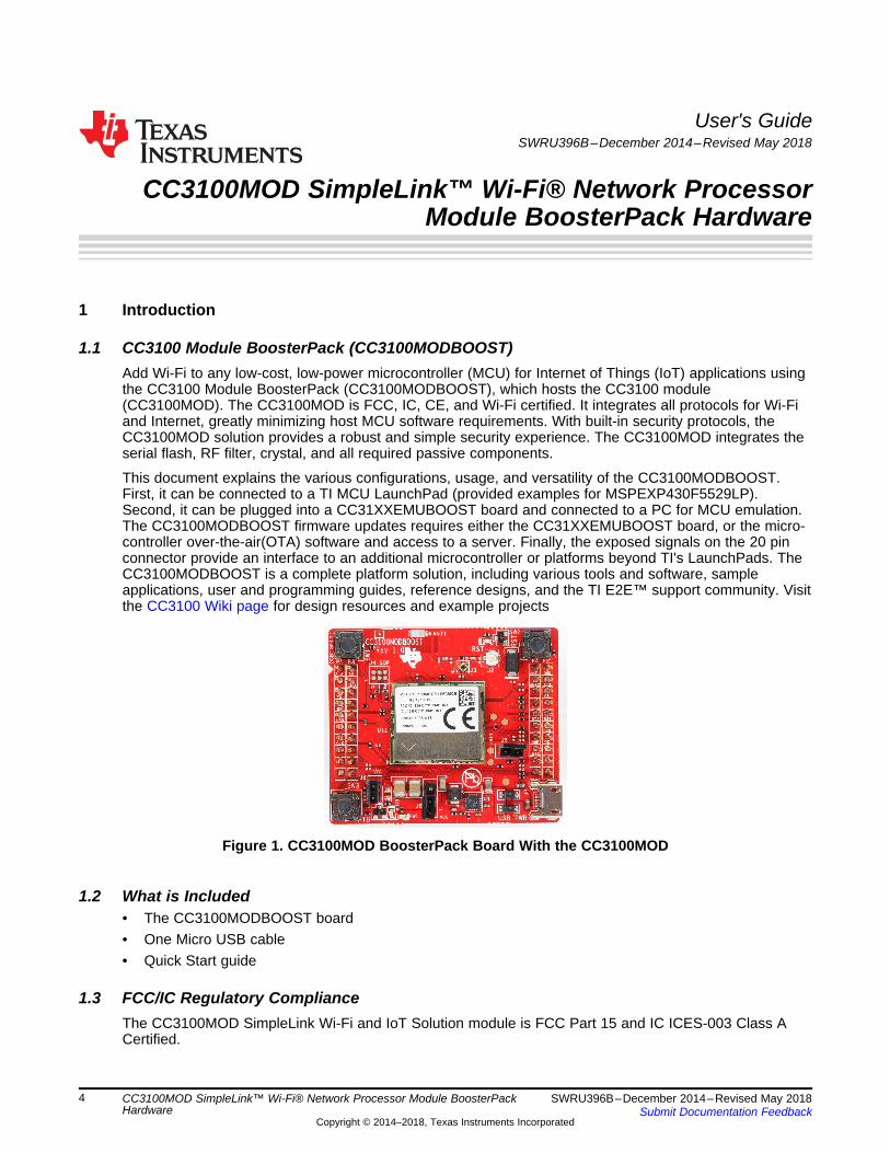
1.1 CC3100 Module BoosterPack (CC3100MODBOOST)Add Wi-Fi to any low-cost, low-power microcontroller (MCU) for Internet of Things (IoT) applications usingthe CC3100 Module BoosterPack (CC3100MODBOOST), which hosts the CC3100 module(CC3100MOD). The CC3100MOD is FCC, IC, CE, and Wi-Fi certified. It integrates all protocols for Wi-Fiand Internet, greatly minimizing host MCU software requirements. With built-in security protocols, theCC3100MOD solution provides a robust and simple security experience. The CC3100MOD integrates theserial flash, RF filter, crystal, and all required passive components.
This document explains the various configurations, usage, and versatility of the CC3100MODBOOST.First, it can be connected to a TI MCU LaunchPad (provided examples for MSPEXP430F5529LP).Second, it can be plugged into a CC31XXEMUBOOST board and connected to a PC for MCU emulation.The CC3100MODBOOST firmware updates requires either the CC31XXEMUBOOST board, or the micro-controller over-the-air(OTA) software and access to a server. Finally, the exposed signals on the 20 pinconnector provide an interface to an additional microcontroller or platforms beyond TI's LaunchPads. TheCC3100MODBOOST is a complete platform solution, including various tools and software, sampleapplications, user and programming guides, reference designs, and the TI E2E™ support community. Visitthe CC3100 Wiki page for design resources and example projects
Figure 1. CC3100MOD BoosterPack Board With the CC3100MOD
1.2 What is Included• The CC3100MODBOOST board• One Micro USB cable• Quick Start guide
1.3 FCC/IC Regulatory ComplianceThe CC3100MOD SimpleLink Wi-Fi and IoT Solution module is FCC Part 15 and IC ICES-003 Class ACertified.
www.ti.com Hardware Description
5SWRU396B–December 2014–Revised May 2018Submit Documentation Feedback
Copyright © 2014–2018, Texas Instruments Incorporated
CC3100MOD SimpleLink™ Wi-Fi® Network Processor Module BoosterPackHardware
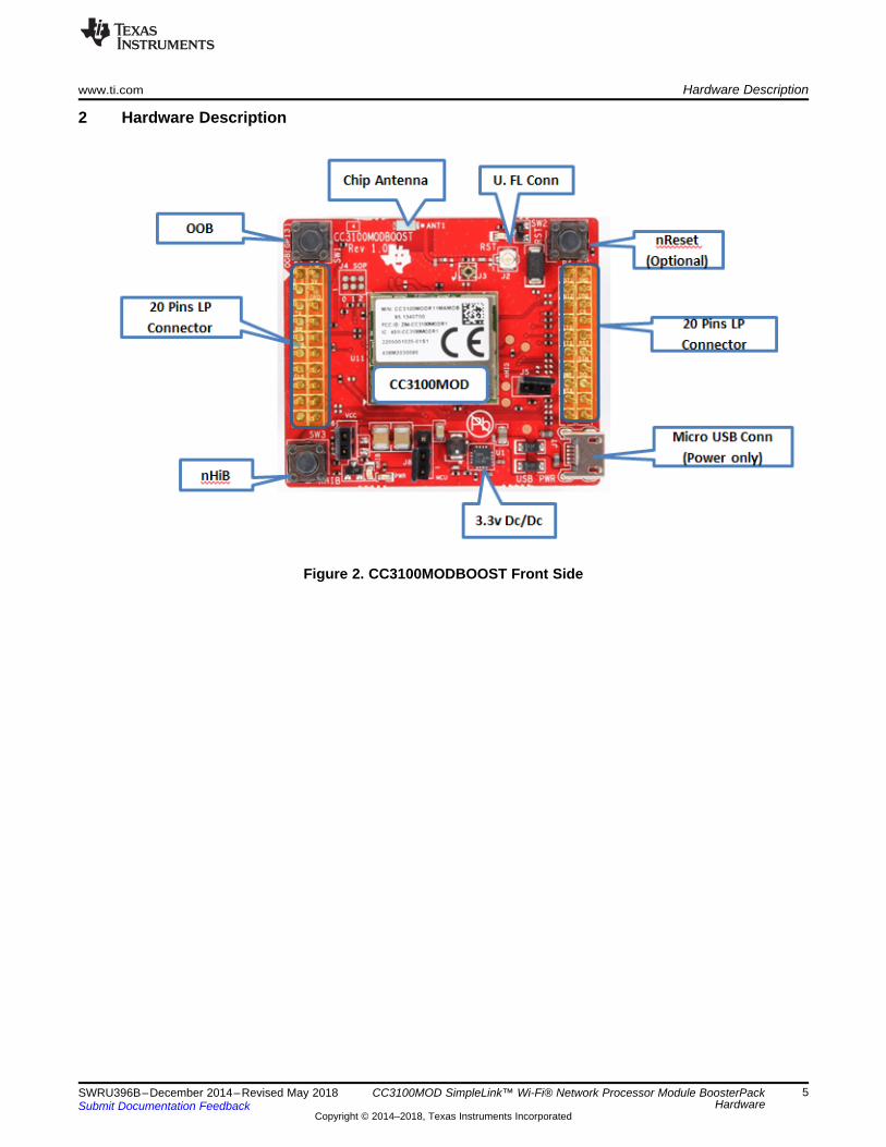
2 Hardware Description
Figure 2. CC3100MODBOOST Front Side
Hardware Description www.ti.com
6 SWRU396B–December 2014–Revised May 2018Submit Documentation Feedback
Copyright © 2014–2018, Texas Instruments Incorporated
CC3100MOD SimpleLink™ Wi-Fi® Network Processor Module BoosterPackHardware
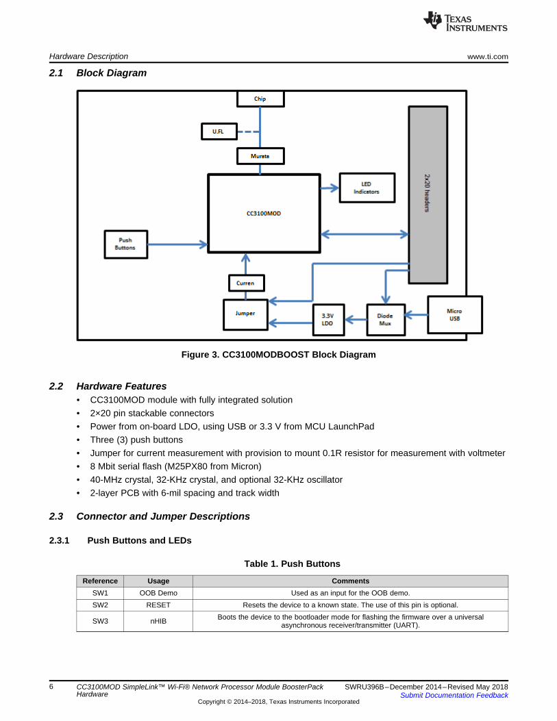
2.1 Block Diagram
Figure 3. CC3100MODBOOST Block Diagram
2.2 Hardware Features• CC3100MOD module with fully integrated solution• 2×20 pin stackable connectors• Power from on-board LDO, using USB or 3.3 V from MCU LaunchPad• Three (3) push buttons• Jumper for current measurement with provision to mount 0.1R resistor for measurement with voltmeter• 8 Mbit serial flash (M25PX80 from Micron)• 40-MHz crystal, 32-KHz crystal, and optional 32-KHz oscillator• 2-layer PCB with 6-mil spacing and track width
2.3 Connector and Jumper Descriptions
2.3.1 Push Buttons and LEDs
Table 1. Push Buttons
Reference Usage CommentsSW1 OOB Demo Used as an input for the OOB demo.SW2 RESET Resets the device to a known state. The use of this pin is optional.
SW3 nHIB Boots the device to the bootloader mode for flashing the firmware over a universalasynchronous receiver/transmitter (UART).
www.ti.com Hardware Description
7SWRU396B–December 2014–Revised May 2018Submit Documentation Feedback
Copyright © 2014–2018, Texas Instruments Incorporated
CC3100MOD SimpleLink™ Wi-Fi® Network Processor Module BoosterPackHardware
Table 2. LEDs
Reference Color Usage CommentsD5 Red PWR Indication ON, when the 3.3-V power is provided to the board.
D1 Yellow nRESET This LED indicates the state of the nRESET pin. If this LED is glowing, the deviceis functional.
D6 Green nHIB This LED indicates the state of the nHIB pin. When the LED is OFF, the device isin hibernate state.
2.3.2 Jumper Settings
Table 3. Jumper Settings
Reference Usage Comments
J7 USB connector For powering the booster pack when mated with a Launchpad. This is mandatory when using“Z” devices. For example, CC3100HZ.
J8 Power selectionChoose the power supply from the Launchpad or the on-board USB.J8 (1-2) power from MCU LaunchpadJ8 (2-3) power from on-board USB using 3.3-V LDO
J6 Currentmeasurement
For Hibernate and LPDS currents, connect an ammeter across J26 : Range (<500 uA)For Active current, mount an 0.1-Ω resistor on R42 and measure the voltage across the 0.1-Ωresistor using a voltmeter. Range (<50 mV peak-peak)
J5 OOB Demo Closed: GPIO_12 is hard pulled to Vcc
Open: GPIO_12 is pulled to GND using 33K resistor.
J10, J9 Booster packheader 2×10 pins each connected to the Launchpad.
J3 RF Test Murata connector (MM8030-2610) for production line tests.J2 RF Test U.FL connector for conducted testing in the lab.
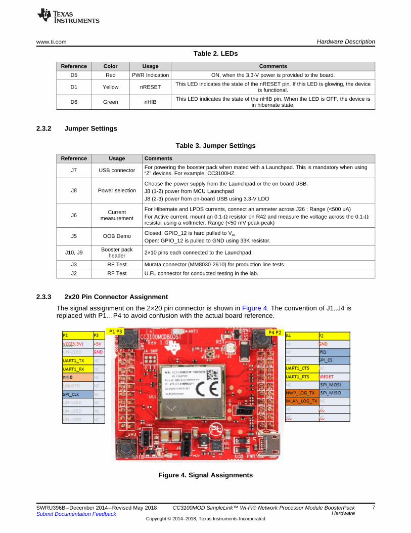
2.3.3 2x20 Pin Connector AssignmentThe signal assignment on the 2×20 pin connector is shown in Figure 4. The convention of J1..J4 isreplaced with P1…P4 to avoid confusion with the actual board reference.
Figure 4. Signal Assignments
Hardware Description www.ti.com
8 SWRU396B–December 2014–Revised May 2018Submit Documentation Feedback
Copyright © 2014–2018, Texas Instruments Incorporated
CC3100MOD SimpleLink™ Wi-Fi® Network Processor Module BoosterPackHardware
Table 4. Outer Row Connectors
Pin No Signal Name Direction Pin No Signal Name DirectionP1.1 VCC (3.3 V) IN P2.1 GND INP1.2 UNUSED NA P2.2 IRQ OUTP1.3 UART1_TX OUT P2.3 SPI_CS INP1.4 UART1_TX IN P2.4 UNUSED NAP1.5 nHIB IN P2.5 nRESET INP1.6 UNUSED NA P2.6 SPI_MOSI INP1.7 SPI_CLK IN P2.7 SPI_MISO OUTP1.8 UNUSED NA P2.8 UNUSED NAP1.9 UNUSED NA P2.9 UNUSED NAP1.10 UNUSED NA P2.10 UNUSED NA
Table 5. Inner Row Connectors
Pin No Signal Name Direction Pin No Signal Name DirectionP3.1 +5 V IN P4.1 UNUSED OUTP3.2 GND IN P4.2 UNUSED OUTP3.3 UNUSED NA P4.3 UNUSED NAP3.4 UNUSED NA P4.4 UART1_CTS INP3.5 UNUSED NA P4.5 UART1_RTS OUTP3.6 UNUSED NA P4.6 UNUSED NAP3.7 UNUSED NA P4.7 NWP_LOG_TX OUTP3.8 UNUSED NA P4.8 WLAN_LOG_TX OUTP3.9 UNUSED NA P4.9 UNUSED INP3.10 UNUSED NA P4.10 UNUSED
NOTE: All signals are 3.3-V CMOS 400-mA logic levels, and are referred w.r.t. CC3100MOD IC.For example, UART1_TX is an output from the CC3100MOD. For the SPI lines, theCC3100MOD always acts like a slave.
2.4 PowerThe board is designed to accept power from a connected LaunchPad or from the CC3100EMUBOOSTboard. Some of the LaunchPads are not capable of sourcing the peak current requirements of Wi-Fi. Inthis case, the USB connector on the CC3100MODBOOST can be used to aid the peak current. The use ofSchottky diodes ensure that the load sharing occurs between the USB connectors on the LaunchPad andthe BoosterPack without any board modifications.
The 3.3-V power can also be sourced from the LaunchPad, or from the 3.3-V LDO on the board by usingjumper J8. If the LaunchPad is not able to source the 3.3 V up to 350 mA, configure the J8 to work fromthe on-board LDO.
2.4.1 Power From the LaunchPad or CC3100EMUBOOSTThe most common scenario is to power the CC3100MODBOOST from the connected LaunchPad. In thiscase, the LaunchPad provides 3.3 V to the BoosterPack for its operation (see Figure 5). In addition to the3.3 V, some LaunchPads provide a 5 V from the USB (see Figure 6), used to drive a 3.3-V LDO on theBoosterPack. If the LaunchPad is not able to provide the 5 V (for example, the LaunchPad with only 20pins), then the USB connector on the CC3100MODBOOST should be used to provide the LDO input asshown below.

www.ti.com Hardware Description
9SWRU396B–December 2014–Revised May 2018Submit Documentation Feedback
Copyright © 2014–2018, Texas Instruments Incorporated
CC3100MOD SimpleLink™ Wi-Fi® Network Processor Module BoosterPackHardware
Figure 5. 3.3-V Power From MCU
Figure 6. Feed USB on the BoosterPack (if the LaunchPad Cannot Source 5 V on 20-Pin Connector)
2.4.2 On-Board LDO Power SupplyOn some LaunchPads, the 3.3 V is not capable of sourcing the 350-mA peak current needed for theCC3100MODBOOST. In this case, the on-board 3.3-V LDO can be used (see Figure 7). This LDO issourced from the USB connector on the CC3100MODBOOST and the LaunchPad in a shared loadmanner.

Hardware Description www.ti.com
10 SWRU396B–December 2014–Revised May 2018Submit Documentation Feedback
Copyright © 2014–2018, Texas Instruments Incorporated
CC3100MOD SimpleLink™ Wi-Fi® Network Processor Module BoosterPackHardware
Figure 7. 3.3-V Power From LDO
Figure 8. Feed USB on the BoosterPack (Always While Using the Onboard LDO)
2.5 Measure the CC3100 Current Drawn
2.5.1 Low Current Measurement (Hibernate and LPDS)To measure the current drawn from the CC3100 device, a jumper is provided on the board labeled J6. Byremoving this jumper, the user can place an ammeter into this path and observe the current. This methodis recommended for measuring LPDS and hibernate currents that are just a few 10s of micro amps. Thejumper is removed and an ammeter is added in series to measure the hibernate and LPDS currents (seeFigure 9).
www.ti.com Hardware Description
11SWRU396B–December 2014–Revised May 2018Submit Documentation Feedback
Copyright © 2014–2018, Texas Instruments Incorporated
CC3100MOD SimpleLink™ Wi-Fi® Network Processor Module BoosterPackHardware
Figure 9. Low Current Measurement
NOTE: If the device uses service pack 1.1.0 or higher, the R113 resistor must be removed to getlower LPDS currents. This resistor can leak an extra 33 uA from the 3.3-V supply in LPDSmode, if the SPI is used as the host interface.
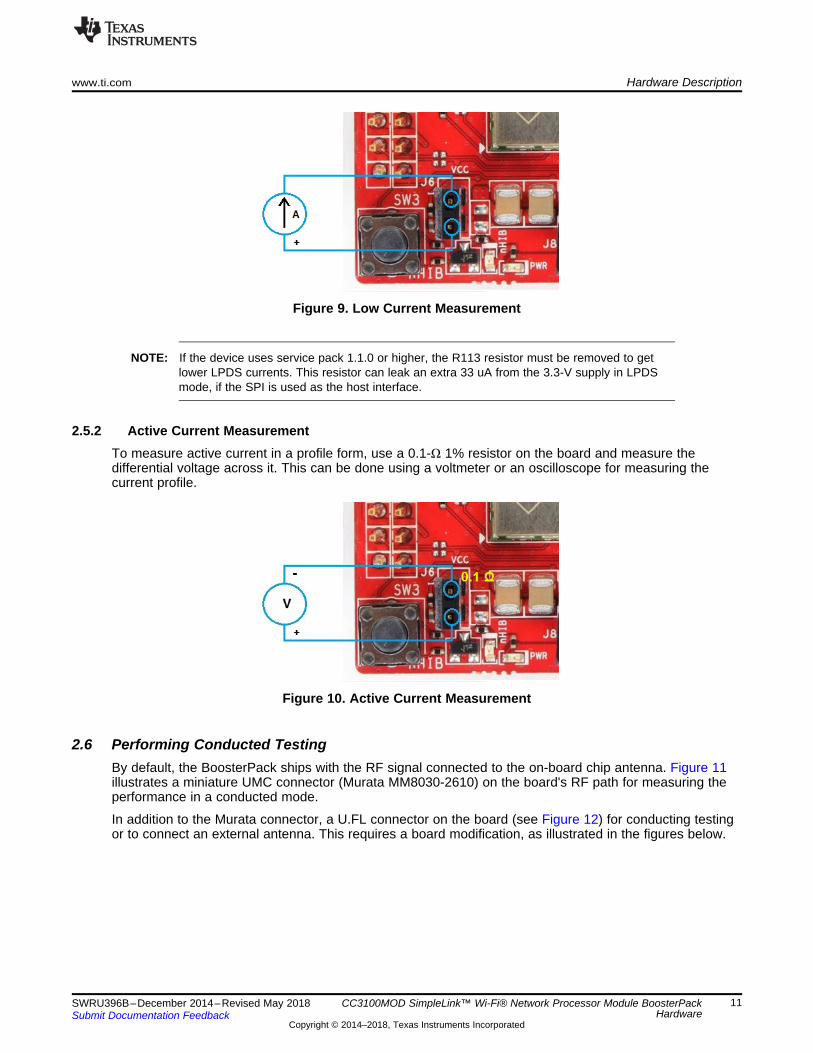
2.5.2 Active Current MeasurementTo measure active current in a profile form, use a 0.1-Ω 1% resistor on the board and measure thedifferential voltage across it. This can be done using a voltmeter or an oscilloscope for measuring thecurrent profile.
Figure 10. Active Current Measurement
2.6 Performing Conducted TestingBy default, the BoosterPack ships with the RF signal connected to the on-board chip antenna. Figure 11illustrates a miniature UMC connector (Murata MM8030-2610) on the board's RF path for measuring theperformance in a conducted mode.
In addition to the Murata connector, a U.FL connector on the board (see Figure 12) for conducting testingor to connect an external antenna. This requires a board modification, as illustrated in the figures below.

Hardware Description www.ti.com
12 SWRU396B–December 2014–Revised May 2018Submit Documentation Feedback
Copyright © 2014–2018, Texas Instruments Incorporated
CC3100MOD SimpleLink™ Wi-Fi® Network Processor Module BoosterPackHardware
Figure 11. Connectors on the Board
Figure 12. Resistor Switch for Radiated versus Conducted Tests
www.ti.com Connecting to the PC Using EMUBOOST
13SWRU396B–December 2014–Revised May 2018Submit Documentation Feedback
Copyright © 2014–2018, Texas Instruments Incorporated
CC3100MOD SimpleLink™ Wi-Fi® Network Processor Module BoosterPackHardware
3 Connecting to the PC Using EMUBOOST
3.1 CC31XXEMUBOOST
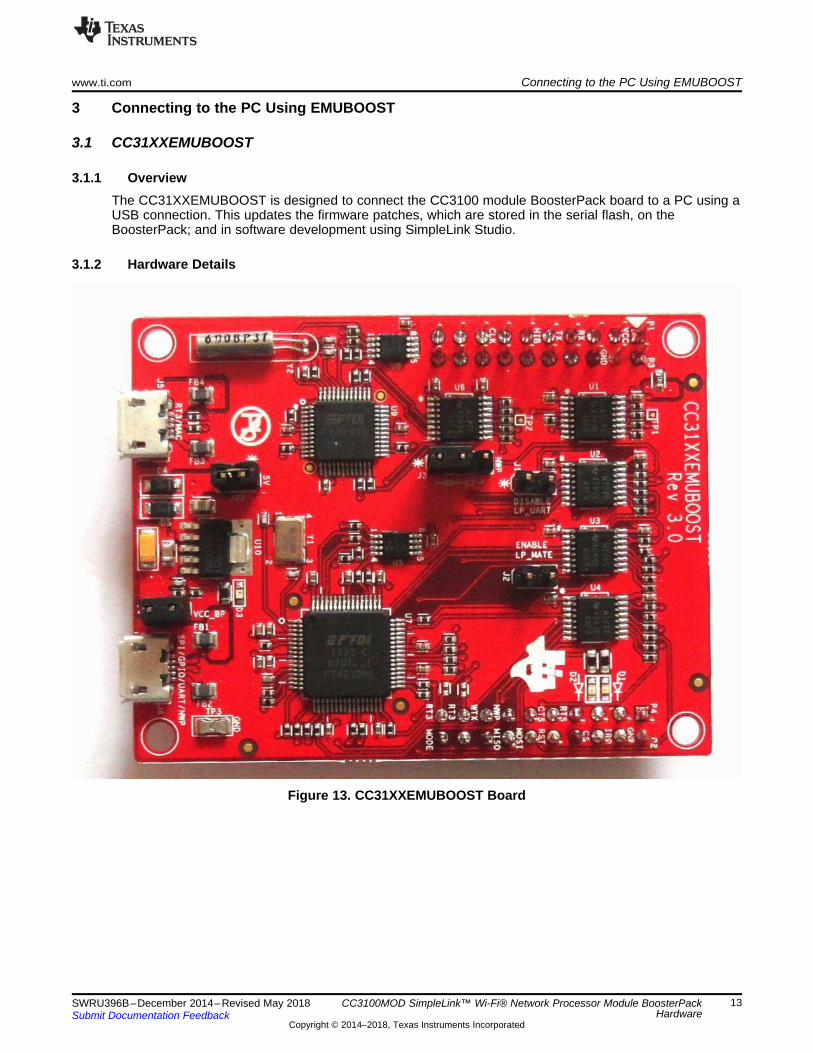
3.1.1 OverviewThe CC31XXEMUBOOST is designed to connect the CC3100 module BoosterPack board to a PC using aUSB connection. This updates the firmware patches, which are stored in the serial flash, on theBoosterPack; and in software development using SimpleLink Studio.
3.1.2 Hardware Details
Figure 13. CC31XXEMUBOOST Board
Connecting to the PC Using EMUBOOST www.ti.com
14 SWRU396B–December 2014–Revised May 2018Submit Documentation Feedback
Copyright © 2014–2018, Texas Instruments Incorporated
CC3100MOD SimpleLink™ Wi-Fi® Network Processor Module BoosterPackHardware
The board has two FTDI ICs to enumerate multiple COM and D2XX ports. The details of the ports aregiven in Table 6.
Table 6. Ports Available on J6
PortNumber Port Type Usage Comments
1 D2XX SPI port for SL Studio2 D2XX GPIO for SL Studio Control the nRESET, nHIB, IRQ
3 VCP COM port for Flashprogramming
4 VCP NWP Network processor logger output. Used with specific tools to analyze thenetwork processor logs. For TI use only.
NOTE: On the PC, only two of the four ports are visible on the Device Manager. The D2XX ports arenot listed under the Ports tab.
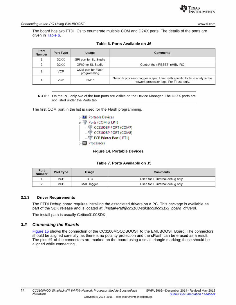
The first COM port in the list is used for the Flash programming.
Figure 14. Portable Devices
Table 7. Ports Available on J5
PortNumber Port Type Usage Comments
1 VCP RT3 Used for TI internal debug only.2 VCP MAC logger Used for TI internal debug only.
3.1.3 Driver RequirementsThe FTDI Debug board requires installing the associated drivers on a PC. This package is available aspart of the SDK release and is located at: [Install-Path]\cc3100-sdk\tools\cc31xx_board_drivers\.
The install path is usually C:\ti\cc3100SDK.
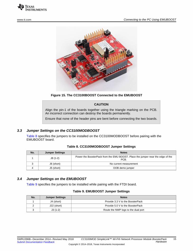
3.2 Connecting the BoardsFigure 15 shows the connection of the CC3100MOODBOOST to the EMUBOOST Board. The connectorsshould be aligned carefully, as there is no polarity protection and the sFlash can be erased as a result.The pins #1 of the connectors are marked on the board using a small triangle marking; these should bealigned while connecting.
www.ti.com Connecting to the PC Using EMUBOOST
15SWRU396B–December 2014–Revised May 2018Submit Documentation Feedback
Copyright © 2014–2018, Texas Instruments Incorporated
CC3100MOD SimpleLink™ Wi-Fi® Network Processor Module BoosterPackHardware
Figure 15. The CC3100BOOST Connected to the EMUBOOST
CAUTIONAlign the pin-1 of the boards together using the triangle marking on the PCB.An incorrect connection can destroy the boards permanently.
Ensure that none of the header pins are bent before connecting the two boards.
3.3 Jumper Settings on the CC3100MODBOOSTTable 8 specifies the jumpers to be installed on the CC3100MODBOOST before pairing with theEMUBOOST board.
Table 8. CC3100MODBOOST Jumper Settings
No. Jumper Settings Notes
1 J8 (1-2) Power the BoosterPack from the EMU BOOST. Place the jumper near the edge of thePCB.
3 J6 (short) No current measurement4 J5 (short) OOB demo jumper
3.4 Jumper Settings on the EMUBOOSTTable 9 specifies the jumpers to be installed while pairing with the FTDI board.
Table 9. EMUBOOST Jumper Settings
No. Jumper Settings Notes1 J4 (short) Provide 3.3 V to the BoosterPack2 J22 (short) Provide 5.0 V to the BoosterPack3 J3 (1-2) Route the NWP logs to the dual port
Connecting to a LaunchPad www.ti.com
16 SWRU396B–December 2014–Revised May 2018Submit Documentation Feedback
Copyright © 2014–2018, Texas Instruments Incorporated
CC3100MOD SimpleLink™ Wi-Fi® Network Processor Module BoosterPackHardware
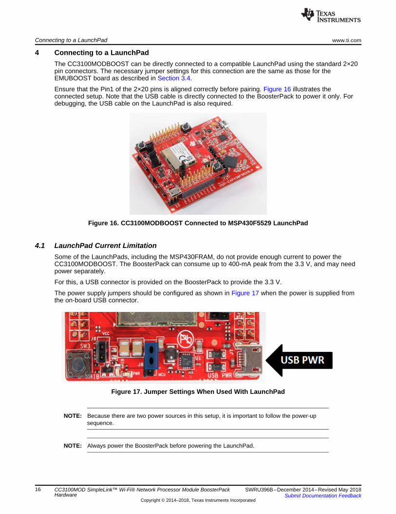
4 Connecting to a LaunchPadThe CC3100MODBOOST can be directly connected to a compatible LaunchPad using the standard 2×20pin connectors. The necessary jumper settings for this connection are the same as those for theEMUBOOST board as described in Section 3.4.
Ensure that the Pin1 of the 2×20 pins is aligned correctly before pairing. Figure 16 illustrates theconnected setup. Note that the USB cable is directly connected to the BoosterPack to power it only. Fordebugging, the USB cable on the LaunchPad is also required.
Figure 16. CC3100MODBOOST Connected to MSP430F5529 LaunchPad
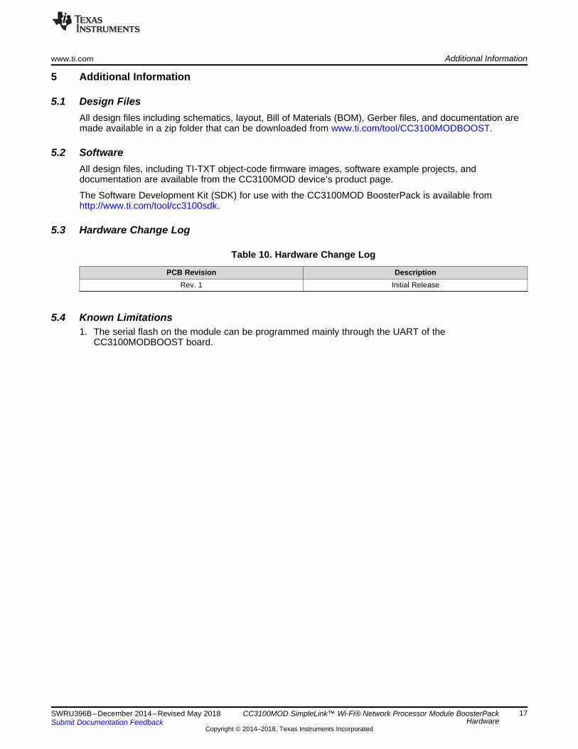
4.1 LaunchPad Current LimitationSome of the LaunchPads, including the MSP430FRAM, do not provide enough current to power theCC3100MODBOOST. The BoosterPack can consume up to 400-mA peak from the 3.3 V, and may needpower separately.
For this, a USB connector is provided on the BoosterPack to provide the 3.3 V.
The power supply jumpers should be configured as shown in Figure 17 when the power is supplied fromthe on-board USB connector.
Figure 17. Jumper Settings When Used With LaunchPad
NOTE: Because there are two power sources in this setup, it is important to follow the power-upsequence.
NOTE: Always power the BoosterPack before powering the LaunchPad.
www.ti.com Additional Information
17SWRU396B–December 2014–Revised May 2018Submit Documentation Feedback
Copyright © 2014–2018, Texas Instruments Incorporated
CC3100MOD SimpleLink™ Wi-Fi® Network Processor Module BoosterPackHardware
5 Additional Information
5.1 Design FilesAll design files including schematics, layout, Bill of Materials (BOM), Gerber files, and documentation aremade available in a zip folder that can be downloaded from www.ti.com/tool/CC3100MODBOOST.
5.2 SoftwareAll design files, including TI-TXT object-code firmware images, software example projects, anddocumentation are available from the CC3100MOD device’s product page.
The Software Development Kit (SDK) for use with the CC3100MOD BoosterPack is available fromhttp://www.ti.com/tool/cc3100sdk.
5.3 Hardware Change Log
Table 10. Hardware Change Log
PCB Revision DescriptionRev. 1 Initial Release
5.4 Known Limitations1. The serial flash on the module can be programmed mainly through the UART of the
CC3100MODBOOST board.
Revision History www.ti.com
18 SWRU396B–December 2014–Revised May 2018Submit Documentation Feedback
Copyright © 2014–2018, Texas Instruments Incorporated
Revision History
Revision HistoryNOTE: Page numbers for previous revisions may differ from page numbers in the current version.
Changes from A Revision (September 2015) to B Revision .......................................................................................... Page
• Updated 3.3-V Power From LDO image. ............................................................................................. 10
STANDARD TERMS FOR EVALUATION MODULES1. Delivery: TI delivers TI evaluation boards, kits, or modules, including any accompanying demonstration software, components,
and/or documentation which may be provided together or separately (collectively, an “EVM” or “EVMs”) to the User (“User”) inaccordance with the terms set forth herein. User's acceptance of the EVM is expressly subject to the following terms.1.1 EVMs are intended solely for product or software developers for use in a research and development setting to facilitate
feasibility evaluation, experimentation, or scientific analysis of TI semiconductors products. EVMs have no direct functionand are not finished products. EVMs shall not be directly or indirectly assembled as a part or subassembly in anyfinished product. For clarification, any software or software tools provided with the EVM (“Software”) shall not be subjectto the terms and conditions set forth herein but rather shall be subject to the applicable terms that accompany suchSoftware
1.2 EVMs are not intended for consumer or household use. EVMs may not be sold, sublicensed, leased, rented, loaned,assigned, or otherwise distributed for commercial purposes by Users, in whole or in part, or used in any finished productor production system.
2 Limited Warranty and Related Remedies/Disclaimers:2.1 These terms do not apply to Software. The warranty, if any, for Software is covered in the applicable Software License
Agreement.2.2 TI warrants that the TI EVM will conform to TI's published specifications for ninety (90) days after the date TI delivers
such EVM to User. Notwithstanding the foregoing, TI shall not be liable for a nonconforming EVM if (a) thenonconformity was caused by neglect, misuse or mistreatment by an entity other than TI, including improper installationor testing, or for any EVMs that have been altered or modified in any way by an entity other than TI, (b) thenonconformity resulted from User's design, specifications or instructions for such EVMs or improper system design, or(c) User has not paid on time. Testing and other quality control techniques are used to the extent TI deems necessary.TI does not test all parameters of each EVM.User's claims against TI under this Section 2 are void if User fails to notify TI of any apparent defects in the EVMs withinten (10) business days after delivery, or of any hidden defects with ten (10) business days after the defect has beendetected.
2.3 TI's sole liability shall be at its option to repair or replace EVMs that fail to conform to the warranty set forth above, orcredit User's account for such EVM. TI's liability under this warranty shall be limited to EVMs that are returned during thewarranty period to the address designated by TI and that are determined by TI not to conform to such warranty. If TIelects to repair or replace such EVM, TI shall have a reasonable time to repair such EVM or provide replacements.Repaired EVMs shall be warranted for the remainder of the original warranty period. Replaced EVMs shall be warrantedfor a new full ninety (90) day warranty period.
3 Regulatory Notices:3.1 United States
3.1.1 Notice applicable to EVMs not FCC-Approved:FCC NOTICE: This kit is designed to allow product developers to evaluate electronic components, circuitry, or softwareassociated with the kit to determine whether to incorporate such items in a finished product and software developers towrite software applications for use with the end product. This kit is not a finished product and when assembled may notbe resold or otherwise marketed unless all required FCC equipment authorizations are first obtained. Operation issubject to the condition that this product not cause harmful interference to licensed radio stations and that this productaccept harmful interference. Unless the assembled kit is designed to operate under part 15, part 18 or part 95 of thischapter, the operator of the kit must operate under the authority of an FCC license holder or must secure anexperimental authorization under part 5 of this chapter.3.1.2 For EVMs annotated as FCC – FEDERAL COMMUNICATIONS COMMISSION Part 15 Compliant:
CAUTIONThis device complies with part 15 of the FCC Rules. Operation is subject to the following two conditions: (1) This devicemay not cause harmful interference, and (2) this device must accept any interference received, including interferencethat may cause undesired operation.Changes or modifications not expressly approved by the party responsible for compliance could void the user's authorityto operate the equipment.
FCC Interference Statement for Class A EVM devices
www.ti.com Revision History
19SWRU396B–December 2014–Revised May 2018Submit Documentation Feedback
Copyright © 2014–2018, Texas Instruments Incorporated
Revision History
STANDARD TERMS FOR EVALUATION MODULES (continued)NOTE: This equipment has been tested and found to comply with the limits for a Class A digital device, pursuant to part15 of the FCC Rules. These limits are designed to provide reasonable protection against harmful interference when theequipment is operated in a commercial environment. This equipment generates, uses, and can radiate radio frequencyenergy and, if not installed and used in accordance with the instruction manual, may cause harmful interference to radiocommunications. Operation of this equipment in a residential area is likely to cause harmful interference in which casethe user will be required to correct the interference at his own expense.
FCC Interference Statement for Class B EVM devicesNOTE: This equipment has been tested and found to comply with the limits for a Class B digital device, pursuant to part15 of the FCC Rules. These limits are designed to provide reasonable protection against harmful interference in aresidential installation. This equipment generates, uses and can radiate radio frequency energy and, if not installed andused in accordance with the instructions, may cause harmful interference to radio communications. However, there is noguarantee that interference will not occur in a particular installation. If this equipment does cause harmful interference toradio or television reception, which can be determined by turning the equipment off and on, the user is encouraged to tryto correct the interference by one or more of the following measures:
• Reorient or relocate the receiving antenna.• Increase the separation between the equipment and receiver.• Connect the equipment into an outlet on a circuit different from that to which the receiver is connected.• Consult the dealer or an experienced radio/TV technician for help.
3.2 Canada3.2.1 For EVMs issued with an Industry Canada Certificate of Conformance to RSS-210 or RSS-247Concerning EVMs Including Radio Transmitters:This device complies with Industry Canada license-exempt RSSs. Operation is subject to the following two conditions:(1) this device may not cause interference, and (2) this device must accept any interference, including interference thatmay cause undesired operation of the device.
Concernant les EVMs avec appareils radio:Le présent appareil est conforme aux CNR d'Industrie Canada applicables aux appareils radio exempts de licence.L'exploitation est autorisée aux deux conditions suivantes: (1) l'appareil ne doit pas produire de brouillage, et (2)l'utilisateur de l'appareil doit accepter tout brouillage radioélectrique subi, même si le brouillage est susceptible d'encompromettre le fonctionnement.
Concerning EVMs Including Detachable Antennas:Under Industry Canada regulations, this radio transmitter may only operate using an antenna of a type and maximum (orlesser) gain approved for the transmitter by Industry Canada. To reduce potential radio interference to other users, theantenna type and its gain should be so chosen that the equivalent isotropically radiated power (e.i.r.p.) is not more thanthat necessary for successful communication. This radio transmitter has been approved by Industry Canada to operatewith the antenna types listed in the user guide with the maximum permissible gain and required antenna impedance foreach antenna type indicated. Antenna types not included in this list, having a gain greater than the maximum gainindicated for that type, are strictly prohibited for use with this device.
Concernant les EVMs avec antennes détachablesConformément à la réglementation d'Industrie Canada, le présent émetteur radio peut fonctionner avec une antenned'un type et d'un gain maximal (ou inférieur) approuvé pour l'émetteur par Industrie Canada. Dans le but de réduire lesrisques de brouillage radioélectrique à l'intention des autres utilisateurs, il faut choisir le type d'antenne et son gain desorte que la puissance isotrope rayonnée équivalente (p.i.r.e.) ne dépasse pas l'intensité nécessaire à l'établissementd'une communication satisfaisante. Le présent émetteur radio a été approuvé par Industrie Canada pour fonctionneravec les types d'antenne énumérés dans le manuel d’usage et ayant un gain admissible maximal et l'impédance requisepour chaque type d'antenne. Les types d'antenne non inclus dans cette liste, ou dont le gain est supérieur au gainmaximal indiqué, sont strictement interdits pour l'exploitation de l'émetteur
3.3 Japan3.3.1 Notice for EVMs delivered in Japan: Please see http://www.tij.co.jp/lsds/ti_ja/general/eStore/notice_01.page 日本
国内に輸入される評価用キット、ボードについては、次のところをご覧ください。http://www.tij.co.jp/lsds/ti_ja/general/eStore/notice_01.page
Revision History www.ti.com
20 SWRU396B–December 2014–Revised May 2018Submit Documentation Feedback
Copyright © 2014–2018, Texas Instruments Incorporated
Revision History
STANDARD TERMS FOR EVALUATION MODULES (continued)3.3.2 Notice for Users of EVMs Considered “Radio Frequency Products” in Japan: EVMs entering Japan may not be
certified by TI as conforming to Technical Regulations of Radio Law of Japan.If User uses EVMs in Japan, not certified to Technical Regulations of Radio Law of Japan, User is required to follow theinstructions set forth by Radio Law of Japan, which includes, but is not limited to, the instructions below with respect toEVMs (which for the avoidance of doubt are stated strictly for convenience and should be verified by User):1. Use EVMs in a shielded room or any other test facility as defined in the notification #173 issued by Ministry of
Internal Affairs and Communications on March 28, 2006, based on Sub-section 1.1 of Article 6 of the Ministry’s Rulefor Enforcement of Radio Law of Japan,
2. Use EVMs only after User obtains the license of Test Radio Station as provided in Radio Law of Japan with respectto EVMs, or
3. Use of EVMs only after User obtains the Technical Regulations Conformity Certification as provided in Radio Law ofJapan with respect to EVMs. Also, do not transfer EVMs, unless User gives the same notice above to the transferee.Please note that if User does not follow the instructions above, User will be subject to penalties of Radio Law ofJapan.
【無線電波を送信する製品の開発キットをお使いになる際の注意事項】 開発キットの中には技術基準適合証明を受けていないものがあります。 技術適合証明を受けていないもののご使用に際しては、電波法遵守のため、以下のいずれかの措置を取っていただく必要がありますのでご注意ください。1. 電波法施行規則第6条第1項第1号に基づく平成18年3月28日総務省告示第173号で定められた電波暗室等の試験設備
でご使用いただく。2. 実験局の免許を取得後ご使用いただく。3. 技術基準適合証明を取得後ご使用いただく。
なお、本製品は、上記の「ご使用にあたっての注意」を譲渡先、移転先に通知しない限り、譲渡、移転できないものとします。
上記を遵守頂けない場合は、電波法の罰則が適用される可能性があることをご留意ください。 日本テキサス・イ
ンスツルメンツ株式会社東京都新宿区西新宿6丁目24番1号西新宿三井ビル
3.3.3 Notice for EVMs for Power Line Communication: Please seehttp://www.tij.co.jp/lsds/ti_ja/general/eStore/notice_02.page電力線搬送波通信についての開発キットをお使いになる際の注意事項については、次のところをご覧ください。http://www.tij.co.jp/lsds/ti_ja/general/eStore/notice_02.page
3.4 European Union3.4.1 For EVMs subject to EU Directive 2014/30/EU (Electromagnetic Compatibility Directive):
This is a class A product intended for use in environments other than domestic environments that are connectedto a low-voltage power-supply network that supplies buildings used for domestic purposes. In a domesticenvironment this product may cause radio interference in which case the user may be required to take adequatemeasures.
4 EVM Use Restrictions and Warnings:4.1 EVMS ARE NOT FOR USE IN FUNCTIONAL SAFETY AND/OR SAFETY CRITICAL EVALUATIONS, INCLUDING BUT
NOT LIMITED TO EVALUATIONS OF LIFE SUPPORT APPLICATIONS.4.2 User must read and apply the user guide and other available documentation provided by TI regarding the EVM prior to
handling or using the EVM, including without limitation any warning or restriction notices. The notices contain importantsafety information related to, for example, temperatures and voltages.
4.3 Safety-Related Warnings and Restrictions:
www.ti.com Revision History
21SWRU396B–December 2014–Revised May 2018Submit Documentation Feedback
Copyright © 2014–2018, Texas Instruments Incorporated
Revision History
STANDARD TERMS FOR EVALUATION MODULES (continued)4.3.1 User shall operate the EVM within TI’s recommended specifications and environmental considerations stated in
the user guide, other available documentation provided by TI, and any other applicable requirements and employreasonable and customary safeguards. Exceeding the specified performance ratings and specifications(including but not limited to input and output voltage, current, power, and environmental ranges) for the EVMmay cause personal injury or death, or property damage. If there are questions concerning performance ratingsand specifications, User should contact a TI field representative prior to connecting interface electronics includinginput power and intended loads. Any loads applied outside of the specified output range may also result inunintended and/or inaccurate operation and/or possible permanent damage to the EVM and/or interfaceelectronics. Please consult the EVM user guide prior to connecting any load to the EVM output. If there isuncertainty as to the load specification, please contact a TI field representative. During normal operation, evenwith the inputs and outputs kept within the specified allowable ranges, some circuit components may haveelevated case temperatures. These components include but are not limited to linear regulators, switchingtransistors, pass transistors, current sense resistors, and heat sinks, which can be identified using theinformation in the associated documentation. When working with the EVM, please be aware that the EVM maybecome very warm.
4.3.2 EVMs are intended solely for use by technically qualified, professional electronics experts who are familiar withthe dangers and application risks associated with handling electrical mechanical components, systems, andsubsystems. User assumes all responsibility and liability for proper and safe handling and use of the EVM byUser or its employees, affiliates, contractors or designees. User assumes all responsibility and liability to ensurethat any interfaces (electronic and/or mechanical) between the EVM and any human body are designed withsuitable isolation and means to safely limit accessible leakage currents to minimize the risk of electrical shockhazard. User assumes all responsibility and liability for any improper or unsafe handling or use of the EVM byUser or its employees, affiliates, contractors or designees.
4.4 User assumes all responsibility and liability to determine whether the EVM is subject to any applicable international,federal, state, or local laws and regulations related to User’s handling and use of the EVM and, if applicable, Userassumes all responsibility and liability for compliance in all respects with such laws and regulations. User assumes allresponsibility and liability for proper disposal and recycling of the EVM consistent with all applicable international,federal, state, and local requirements.
5. Accuracy of Information: To the extent TI provides information on the availability and function of EVMs, TI attempts to be asaccurate as possible. However, TI does not warrant the accuracy of EVM descriptions, EVM availability or other informationon its websites as accurate, complete, reliable, current, or error-free.
6. Disclaimers:6.1 EXCEPT AS SET FORTH ABOVE, EVMS AND ANY MATERIALS PROVIDED WITH THE EVM (INCLUDING, BUT NOT
LIMITED TO, REFERENCE DESIGNS AND THE DESIGN OF THE EVM ITSELF) ARE PROVIDED "AS IS" AND "WITHALL FAULTS." TI DISCLAIMS ALL OTHER WARRANTIES, EXPRESS OR IMPLIED, REGARDING SUCH ITEMS,INCLUDING BUT NOT LIMITED TO ANY EPIDEMIC FAILURE WARRANTY OR IMPLIED WARRANTIES OFMERCHANTABILITY OR FITNESS FOR A PARTICULAR PURPOSE OR NON-INFRINGEMENT OF ANY THIRDPARTY PATENTS, COPYRIGHTS, TRADE SECRETS OR OTHER INTELLECTUAL PROPERTY RIGHTS.
6.2 EXCEPT FOR THE LIMITED RIGHT TO USE THE EVM SET FORTH HEREIN, NOTHING IN THESE TERMS SHALLBE CONSTRUED AS GRANTING OR CONFERRING ANY RIGHTS BY LICENSE, PATENT, OR ANY OTHERINDUSTRIAL OR INTELLECTUAL PROPERTY RIGHT OF TI, ITS SUPPLIERS/LICENSORS OR ANY OTHER THIRDPARTY, TO USE THE EVM IN ANY FINISHED END-USER OR READY-TO-USE FINAL PRODUCT, OR FOR ANYINVENTION, DISCOVERY OR IMPROVEMENT, REGARDLESS OF WHEN MADE, CONCEIVED OR ACQUIRED.
7. USER'S INDEMNITY OBLIGATIONS AND REPRESENTATIONS. USER WILL DEFEND, INDEMNIFY AND HOLD TI, ITSLICENSORS AND THEIR REPRESENTATIVES HARMLESS FROM AND AGAINST ANY AND ALL CLAIMS, DAMAGES,LOSSES, EXPENSES, COSTS AND LIABILITIES (COLLECTIVELY, "CLAIMS") ARISING OUT OF OR IN CONNECTIONWITH ANY HANDLING OR USE OF THE EVM THAT IS NOT IN ACCORDANCE WITH THESE TERMS. THIS OBLIGATIONSHALL APPLY WHETHER CLAIMS ARISE UNDER STATUTE, REGULATION, OR THE LAW OF TORT, CONTRACT ORANY OTHER LEGAL THEORY, AND EVEN IF THE EVM FAILS TO PERFORM AS DESCRIBED OR EXPECTED.
8. Limitations on Damages and Liability:
Revision History www.ti.com
22 SWRU396B–December 2014–Revised May 2018Submit Documentation Feedback
Copyright © 2014–2018, Texas Instruments Incorporated
Revision History
STANDARD TERMS FOR EVALUATION MODULES (continued)8.1 General Limitations. IN NO EVENT SHALL TI BE LIABLE FOR ANY SPECIAL, COLLATERAL, INDIRECT, PUNITIVE,
INCIDENTAL, CONSEQUENTIAL, OR EXEMPLARY DAMAGES IN CONNECTION WITH OR ARISING OUT OFTHESE TERMS OR THE USE OF THE EVMS , REGARDLESS OF WHETHER TI HAS BEEN ADVISED OF THEPOSSIBILITY OF SUCH DAMAGES. EXCLUDED DAMAGES INCLUDE, BUT ARE NOT LIMITED TO, COST OFREMOVAL OR REINSTALLATION, ANCILLARY COSTS TO THE PROCUREMENT OF SUBSTITUTE GOODS ORSERVICES, RETESTING, OUTSIDE COMPUTER TIME, LABOR COSTS, LOSS OF GOODWILL, LOSS OF PROFITS,LOSS OF SAVINGS, LOSS OF USE, LOSS OF DATA, OR BUSINESS INTERRUPTION. NO CLAIM, SUIT OR ACTIONSHALL BE BROUGHT AGAINST TI MORE THAN TWELVE (12) MONTHS AFTER THE EVENT THAT GAVE RISE TOTHE CAUSE OF ACTION HAS OCCURRED.
8.2 Specific Limitations. IN NO EVENT SHALL TI'S AGGREGATE LIABILITY FROM ANY USE OF AN EVM PROVIDEDHEREUNDER, INCLUDING FROM ANY WARRANTY, INDEMITY OR OTHER OBLIGATION ARISING OUT OF OR INCONNECTION WITH THESE TERMS, , EXCEED THE TOTAL AMOUNT PAID TO TI BY USER FOR THEPARTICULAR EVM(S) AT ISSUE DURING THE PRIOR TWELVE (12) MONTHS WITH RESPECT TO WHICH LOSSESOR DAMAGES ARE CLAIMED. THE EXISTENCE OF MORE THAN ONE CLAIM SHALL NOT ENLARGE OR EXTENDTHIS LIMIT.
9. Return Policy. Except as otherwise provided, TI does not offer any refunds, returns, or exchanges. Furthermore, no return ofEVM(s) will be accepted if the package has been opened and no return of the EVM(s) will be accepted if they are damaged orotherwise not in a resalable condition. If User feels it has been incorrectly charged for the EVM(s) it ordered or that deliveryviolates the applicable order, User should contact TI. All refunds will be made in full within thirty (30) working days from thereturn of the components(s), excluding any postage or packaging costs.
10. Governing Law: These terms and conditions shall be governed by and interpreted in accordance with the laws of the State ofTexas, without reference to conflict-of-laws principles. User agrees that non-exclusive jurisdiction for any dispute arising out ofor relating to these terms and conditions lies within courts located in the State of Texas and consents to venue in DallasCounty, Texas. Notwithstanding the foregoing, any judgment may be enforced in any United States or foreign court, and TImay seek injunctive relief in any United States or foreign court.
IMPORTANT NOTICE FOR TI DESIGN INFORMATION AND RESOURCES
Texas Instruments Incorporated (‘TI”) technical, application or other design advice, services or information, including, but not limited to,reference designs and materials relating to evaluation modules, (collectively, “TI Resources”) are intended to assist designers who aredeveloping applications that incorporate TI products; by downloading, accessing or using any particular TI Resource in any way, you(individually or, if you are acting on behalf of a company, your company) agree to use it solely for this purpose and subject to the terms ofthis Notice.TI’s provision of TI Resources does not expand or otherwise alter TI’s applicable published warranties or warranty disclaimers for TIproducts, and no additional obligations or liabilities arise from TI providing such TI Resources. TI reserves the right to make corrections,enhancements, improvements and other changes to its TI Resources.You understand and agree that you remain responsible for using your independent analysis, evaluation and judgment in designing yourapplications and that you have full and exclusive responsibility to assure the safety of your applications and compliance of your applications(and of all TI products used in or for your applications) with all applicable regulations, laws and other applicable requirements. Yourepresent that, with respect to your applications, you have all the necessary expertise to create and implement safeguards that (1)anticipate dangerous consequences of failures, (2) monitor failures and their consequences, and (3) lessen the likelihood of failures thatmight cause harm and take appropriate actions. You agree that prior to using or distributing any applications that include TI products, youwill thoroughly test such applications and the functionality of such TI products as used in such applications. TI has not conducted anytesting other than that specifically described in the published documentation for a particular TI Resource.You are authorized to use, copy and modify any individual TI Resource only in connection with the development of applications that includethe TI product(s) identified in such TI Resource. NO OTHER LICENSE, EXPRESS OR IMPLIED, BY ESTOPPEL OR OTHERWISE TOANY OTHER TI INTELLECTUAL PROPERTY RIGHT, AND NO LICENSE TO ANY TECHNOLOGY OR INTELLECTUAL PROPERTYRIGHT OF TI OR ANY THIRD PARTY IS GRANTED HEREIN, including but not limited to any patent right, copyright, mask work right, orother intellectual property right relating to any combination, machine, or process in which TI products or services are used. Informationregarding or referencing third-party products or services does not constitute a license to use such products or services, or a warranty orendorsement thereof. Use of TI Resources may require a license from a third party under the patents or other intellectual property of thethird party, or a license from TI under the patents or other intellectual property of TI.TI RESOURCES ARE PROVIDED “AS IS” AND WITH ALL FAULTS. TI DISCLAIMS ALL OTHER WARRANTIES ORREPRESENTATIONS, EXPRESS OR IMPLIED, REGARDING TI RESOURCES OR USE THEREOF, INCLUDING BUT NOT LIMITED TOACCURACY OR COMPLETENESS, TITLE, ANY EPIDEMIC FAILURE WARRANTY AND ANY IMPLIED WARRANTIES OFMERCHANTABILITY, FITNESS FOR A PARTICULAR PURPOSE, AND NON-INFRINGEMENT OF ANY THIRD PARTY INTELLECTUALPROPERTY RIGHTS.TI SHALL NOT BE LIABLE FOR AND SHALL NOT DEFEND OR INDEMNIFY YOU AGAINST ANY CLAIM, INCLUDING BUT NOTLIMITED TO ANY INFRINGEMENT CLAIM THAT RELATES TO OR IS BASED ON ANY COMBINATION OF PRODUCTS EVEN IFDESCRIBED IN TI RESOURCES OR OTHERWISE. IN NO EVENT SHALL TI BE LIABLE FOR ANY ACTUAL, DIRECT, SPECIAL,COLLATERAL, INDIRECT, PUNITIVE, INCIDENTAL, CONSEQUENTIAL OR EXEMPLARY DAMAGES IN CONNECTION WITH ORARISING OUT OF TI RESOURCES OR USE THEREOF, AND REGARDLESS OF WHETHER TI HAS BEEN ADVISED OF THEPOSSIBILITY OF SUCH DAMAGES.You agree to fully indemnify TI and its representatives against any damages, costs, losses, and/or liabilities arising out of your non-compliance with the terms and provisions of this Notice.This Notice applies to TI Resources. Additional terms apply to the use and purchase of certain types of materials, TI products and services.These include; without limitation, TI’s standard terms for semiconductor products http://www.ti.com/sc/docs/stdterms.htm), evaluationmodules, and samples (http://www.ti.com/sc/docs/sampterms.htm).
Mailing Address: Texas Instruments, Post Office Box 655303, Dallas, Texas 75265Copyright © 2018, Texas Instruments Incorporated