Embed Size (px)
Citation preview
Proc. SNIC Svmp., Stanford, CA, 3-6April(2006) Invited talk
CCD AND PIN-CMOS DEVELOPMENTS FOR LARGE OPTICAL TELESCOPE*
Veljko Radeka Brookhaven National Laboratory
Upton, NY 11973
April, 2006
BNL-76772-2006-CP
*This manuscript has been authored by Brookhaven Science Associates, LLC under Contract No. DE-AC02-98CH10886 with the U.S. Department of Energy. The United States Government retains, and the publisher, by accepting the article for publication, acknowledges, a world-wide license to publish or reproduce the published form of t h s manuscript, or allow others to do so, for the United States Government purposes.
DISCLAIMER
This work was prepared as an accou zt of work sponsored by an agency of the United
any of their employees, nor any of the r contractors, subcontractors, or their employees, makes any warranty, express or inipli 4 d, or assumes any legal liability or responsibility for the accuracy, completeness, or any third party's use or the results of such use of any information, apparatus, product, or process disclosed, or represents that its use would not iitfringe privately owned rights. Reference herein to any specific commercial product, process, or service by trade name, trademark, manufacturer, or otherwise, does not necessarily constitute or imply its endorsement, recommendation, or favoring by the United States Government or any agency thereof or its contractors or subcontractors. The views and opinions of authors expressed herein do not necessarily state or reflect those of the United States Government or any agency thereo$
States Government. Neither the Unit d ,d States Government nor any agency thereox nor
SNIC Symposium, Stanford, California - 3-6 April 2006
CCD and PIN-CMOS Developments for Large Optical Telescopes V. Radeka Brookhaven Nafional Laboratory, Upfon, NY 11973, USA
Higher quantum efficiency in near-IR, narrower point spread function and higher readout speed than with conventional sensors have been receiving increased emphasis in the development of CCDs and silicon PIN-CMOS sensors for use in large optical telescopes. Some key aspects in the development of such devices are reviewed.
I. INTRODUCTION Recent interest in rapid wide area sky surveys in the
optical to near infrared wavelength range has spurred the development of imaging devices, both CCDs and hybrid silicon PN-CMOS sensors beyond the established state- of-the art. Such rapid sky surveys are needed to obtain the statistical accuracy in dark energy studies based on weak lensing. A separate motivation for rapid surveys is to detect and observe fast moving near-earth objects. Wide area surveys require relatively large telescopes with a large field of view. As the field of view is given -
by = (D@/&)z, where D@ is the focal plane
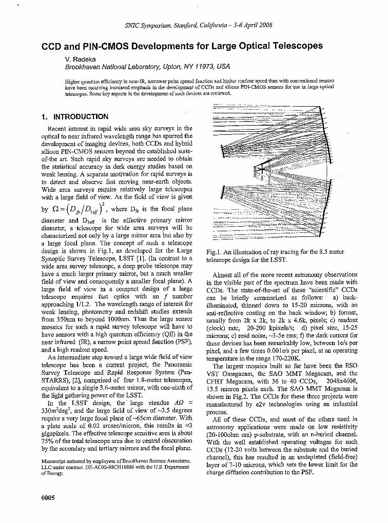
diameter and DleE is the effective primary mirror diameter, a ’telescope for wide area surveys will be characterized not only by a large mirror area but also by a large focal plane. The concept of such a telescope design is shown in Fig.1, as developed for the Large Synoptic Survey Telescope, LSST [l]. (In contrast to a wide area survey telescope, a deep probe telescope may have a much larger primary mirror, but a much smaller field of view and consequently a smaller focal plane). A large field of view in a compact design of a large telescope requires fast optics with an f number approaching U1.2. The wavelength range of interest for weak lensing, photometry and redshift studies extends from 350nm to beyond 1OOOnm. Thus the large sensor mosaics for such a rapid survey telescope will have to have sensors with a high quantum efficiency (QE) in the near infrared (IR), a narrow point spread function (PSF), and a high readout speed.
An intermediate step toward a large wide field of view telescope has been a current project, the Panoramic Survey Telescope and Rapid Response System (Pan- STARRS), [2], comprised of four 1 .%meter telescopes, equivalent to a single 3.6-meter mirror, with one-sixth of the light gathering power of the LSST.
In the LSST design, the‘ large etendue AQ =: 330mzdeg2, and the large field of view of -3.5 degrees require a very large focal plane of -65cm diameter. With a plate scale of 0.02 arcsec/micron, this results in -3 gigapixels. The effective telescope sensitive area is about 75% of the total telescope area due to central obscuration by the secondary and tertiary mirrors and the focal plane.
Manuscript authored by employees of Brookhaven Science Associates, LLC under contract DE-AC02-98CH10886 with the US. Department of Energy.
Fig.1. An illustration of ray tracing for the 8.5 meter telescope design for the LSST.
Almost all of the more recent astronomy observations in the visible part of the spectrum have been made with CCDs. The state-of-the-art of these “scientific” CCDs can be briefly summarized as follows: a) back- illuminated, thinned down to 15-20 microns, with an anti-reflective coating on the back window; b) format, usually from 2k x 2k, to 2k x 4.6k, pixels; c) readout (clock) rate, 20-200 kpixelds; d) pixel size, 15-25 microns; e) read noise, -3-5e rms; f ) the dark current for these devices has been remarkably low, between le/s per pixel, and a few times O.OOle/s per pixel, at an operating temperature in the range 170-220K.
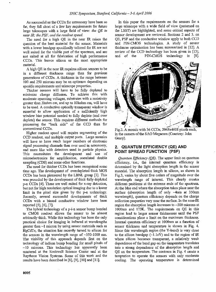
The largest mosaics built so far have been the ESO VST Omegacam, the SA0 MMT Megacam, and the CFHT Megacam, with 36 to 40 CCDs, 2048x4608, 13.5 micron pixels each. The SA0 MMT Megacam is shown in Fig.2. The CCDs for these three projects were manufactured by e2v technologies using an industrial process.
All of these CCDs, and most of the others used in astronomy applications were made on low resistivity (20-1 OOohm cm) p-substrate, with an n-buried channel. With the well established operating voltages for such CCDs (12-20 volts between the substrate and the buried channel), this has resulted in an undepleted (field-free) layer of 7-10 microns, which sets the lower limit for the charge diffusion contribution to the PSF.
0005
SNIC Symposium, Stanford, California - 3-6 April 2006
As successful as the CCDs for astronomy have been so far, they fall short of a few key requirements for future large telescopes with a large field of view: the QE in near IR; the PSF, and the readout speed
The need for a high QE in the near IR raises the question of the best material for the sensor. Materials with a lower bandgap specifically tailored for IR are not well suited for the visible part of the spectrum, and are not suited at all for fabrication of high performance CCDs. This leaves silicon as the most appropriate material.
A high QE in the near IR requires silicon sensors to be in a different thickness range than for previous generations of CCDs. A thickness in the range between 100 and 250 microns may be an optimum depending on specific requirements and telescope properties.
Thicker sensors will have to be fully depleted to minimize charge diffusion. To achieve this with moderate operating voltages, substrates with a resistivity greater than 3kohm cm, and up to 1Okohm cm, will have to be used. A conductive optically transparent window is essential to allow application of a sufficiently high window bias potential needed to fully deplete (and over deplete) the sensor. This requires different methods for processing the “back side” of the CCD than for conventional CCDs.
Higher readout speed will require segmenting of the CCD readout, and multiple output ports. Large mosaics will have to have much larger numbers of electronic signal processing channels than ever used in astronomy, and more like with detectors used in particle physics. This necessitates the development and use of microelectronics for amplification, correlated double sampling (CDS) and some other functions.
The need for thicker CCDs has been recognized some time ago. The development of overdepleted thick MOS CCDs has been pioneered by the LBNL group [3]. This was preceded by the development of thick fully depleted p-n CCDs [4]. These are well suited for x-ray detection, but not for high resolution optical imaging due to a lower limit in the pixel size given by the p-n technology. Recently, several successful developments of thick CCDs with a biased conductive window have been
The hybrid technology of a p-i-n sensor bump bonded to CMOS readout allows the sensor to be almost arbitrarily thick. While this technology has been the only practical choice for imaging in infrared at wavelengths greater than -1 micron by using sensor materials such as HgCdTe, the attention has recently turned to silicon for the sensors in the wavelength range of -350-1000 nm. The viability of this approach depends first on the technology of indium bump bonding for small pixels of -10 microns. This technology has apparently been mastered at the Rockwell Science Center and at the Raytheon Vision Systems. Some of this work and the results have been described in [8], [9], [lo] and [ll].
reported 151, [61,[7l.
In this paper the requirements on the sensors for a large telescope with a wide field of view (patterned on the LSST) are highlighted, and some critical aspects of sensor development are reviewed. Sections 2 and 3. on QE, PSF and the conductive window apply to both CCD and PIN-CMOS technologies. A study of sensor thickness optimization has been summarized in [12]. A review of the CCD technology has been given in [13], and of the PIN-CMOS technology in [8].
Fig.2. A mosaic with 36 CCDs, 2048x4608 pixels each, in the camera of the SA0 Megacam (Courtesy: John Geary).
2. QUANTUM EFFICIENCY (QE) AND POINT SPREAD FUNCTION (PSF)
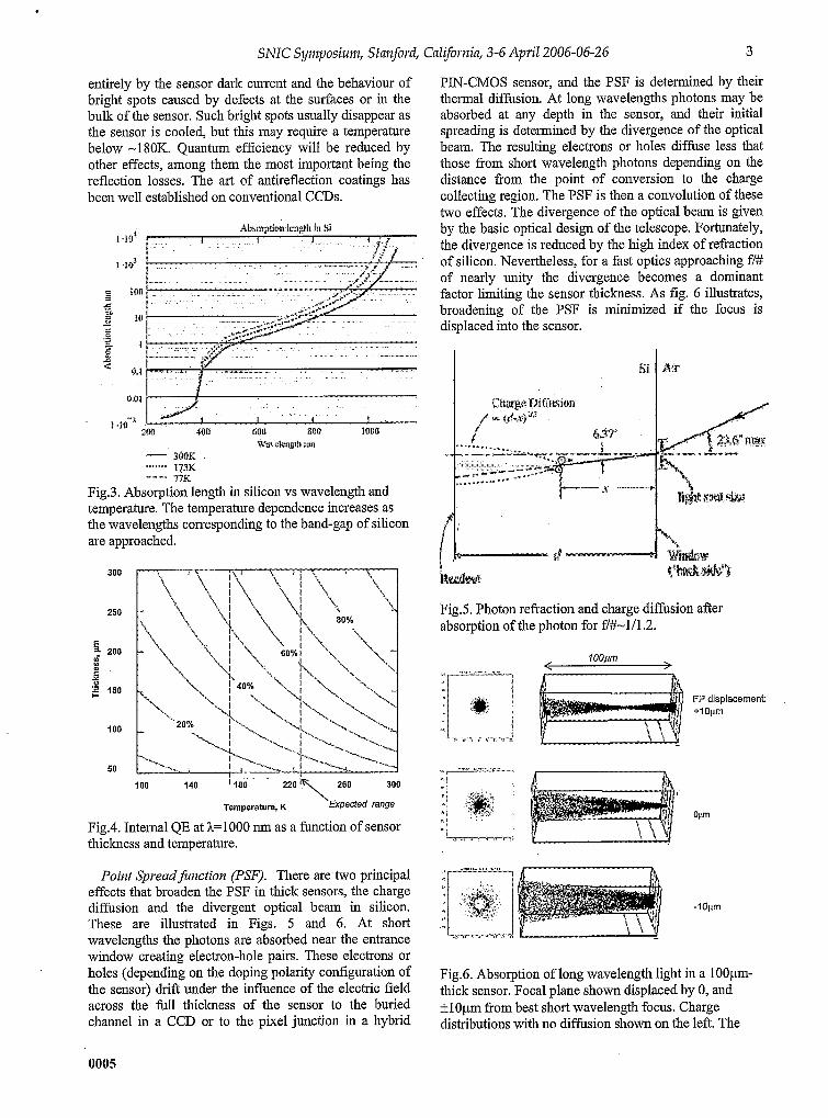
Quantum EfJiciency (QE). The upper limit on quantum efficiency, i.e., the internal quantum efficiency is determined by the light absorption length in the sensor material. The absorption length in silicon, as shown in Fig.3, varies by about five orders of magnitude over the wavelength range of interest. This clearly creates different problems at the extreme ends of the spectrum. At the blue end where the absorption takes place near the surface (absorption length of only -4nm at 350nm wavelength), quantum efficiency depends on the charge collection properties very near the surface. In the near-LR region the absorption length increases to -300 microns at 1OOOnm and 173K. The requirements on QE in this region lead to larger sensor thicknesses until the PSF considerations place a limit on the maximum thickness. Internal quantum efficiency at l O O O n m as a function of sensor thickness and temperature is shown in Fig. 4. Since this wavelength region (the Y-band) is very close to the silicon bandgap (-1.1 eV) and to the region of IR where silicon becomes transparent, a relatively weak dependence of the band gap on the temperature translates into a strong dependence of the absorption length and QE on the temperature. The contours in Fig. 4 create a temptation to operate the sensors with only moderate cooling. The operating temperature is determined
0005
SNIC Synzposiunz, Stanford, Calqornia, 3-6 April 2006-06-26 3
entirely by the sensor dark current and the behaviour of bright spots caused by defects at the surfaces or in the bulk of the sensor. Such bright spots usually disappear as the sensor is cooled, but this may require a temperature below -18OK. Quantum efficiency will be reduced by other effects, among them the most important being the reflection losses. The art of antireflection coatings has been well established on conventional CCDs.
tno
10 I , . *<p+$2+-- 1 .. . ~... ... *+ ". . . . .. . . .. . . . .. . . . . . . . . *.. -. ....
1 .IO'
1 .td
5 e 3 -4 - c TI .-
\va & r I ~ I b uta% 300K I b K 77K
c_ -...... .."__ Fig.3. Absorption length in silicon vs wavelength and temperature. The temperature dependence increases as the wavelengths corresponding to the band-gap of silicon are approached.
300
250
5 200 vi 0
Y
5 150
100
50 100 140 i180- 220 "\ 260 300
Temperature, K Expected range
Fig.4. Internal QE at h=lOOO nm as a function of sensor thickness and temperature.
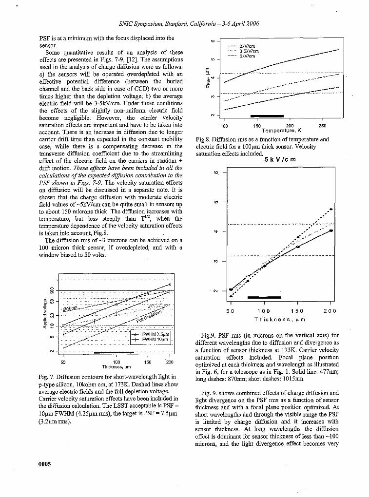
Point Spveadfuriction (PSF). There are two principal effects that broaden the PSF in thick sensors, the charge diffusion and the divergent optical beam in silicon. These are illustrated in Figs. 5 and 6. At short wavelengths the photons are absorbed near the entrance window creating electron-hole pairs. These electrons or holes (depending on the doping polarity configuration of the sensor) drift under the influence of the electric field across the full thickness of the sensor to the buried channel in a CCD or to the pixel junction in a hybrid
PIN-CMOS sensor, and the PSF is determined by their thermal diffusion. At long wavelengths photons may be absorbed at any depth in the sensor, and their initial spreading is deteimined by the divergence of the optical beam. The resulting electrons or holes diffuse less that those from short wavelength photons depending on the distance from the point of conversion to the charge collecting region. The PSF is then a convolution of these two effects. The divergence of the optical beam is given by the basic optical design of the telescope. Fortunately, the divergence is reduced by the high index of refraction of silicon. Nevertheless, for a fast optics approaching E/# of nearly unity the divergence becomes a dominant factor limiting the sensor thickness. As fig. 6 illustrates, broadening of the PSF is minimized if the focus is displaced into the sensor.
si
d k
Rr
Fig.5. Photon refraction and charge diffusion after absorption of the photon for E/#-1/1.2.
-1bprn
Fig.6. Absorption of long wavelength light in a 1OOpm- thick sensor. Focal plane shown displaced by 0, and flOpm ftom best short wavelength focus. Charge distributions with no diffusion shown on the left. The
0005
, SNIC Symposium, Stanford, California - 3-6 April 2006
PSF is at a minimum with the focus displaced into the
effects are presented in Figs. 7-9, [12]. The assumptions
w - PkV/cm sensor. , -
Some quantitative results of an analysis of these
used in the analysis of charge diffusion were as follows: a) the sensors will be operated overdepleted with an effective potential difference (between the buried channel and the back side in case of CCD) two or more times higher than the depletion voltage; b) the average electric field will be 3-5kVlcm. Under these conditions the effects of the slightly non-uniform electric field become negligible. However, the carrier velocity I 1 I I
account. There is an increase in diffusion due to longer carrier drift time than expected in the constant mobility case, while there is a compensating decrease in the transverse diffusion coefficient due to the streamlining effect of the electric field on the carriers in random i- drift motion. These effects have been included in all the calculations of the expected dijiusion contribution to the PSF ShOW77 in Figs. 7-9. The velocity saturation effects on diffusion will be discussed in a separate note. It is shown that the charge diffusion with moderate electric field values of -5kVIcm can be quite small in sensors up to about 150 microns thick. The diffusion increases with temperature, but less steeply than T1”, when the temperature dependence of the velocity saturation effects
The diffusion nns of -3 microns can be achieved on a 100 micron thick sensor, if overdepleted, and with a window biased to 50 volts.
In-
N - - saturation effects are important and have to be taken into 100 150 200 250
Temperature, K Fig.8. Diffusion rms as a function of temperature and electric field for a 100pm thick sensor. Velocity saturation effects included.
5 k V l c m
(D
Lo
is taken into account, Fig.8. TI.
m
cv
5 0 1 0 0 1 5 0 2 0 0 T h i c k n e s s , p m
Fig.9. PSF rms (in microns on the vertical axis) ’for different wavelengths due to diffusion and divergence as a function of sensor thickness at 173K. Carrier velocity saturation effects included. Focal plane position optimized at each thickness and wavelength as illustrated in Fig. 6, for a telescope as in Fig. 1. Solid line: 47711111; long dashes: 87Onm; short dashes: 1 0 1 5 ~ .
_. .,., _. .. ... ... .._ .., ,. .. .. .. ... .. ... ...
50 100 150 200 Thickness, prn
Fig. 7. Diffusion contours for short-wavelength light in p-type silicon, lOkohm cm, at 173K. Dashed lines show average electric fields and the full depletion voltage. Carrier velocity saturation effects have been included in the diffusion calculation. The LSST acceptable is PSF = l o p FWHM ( 4 . 2 5 P rms), the target is PSF = 7.5IJ-m (3.2pm rms).
Fig. 9. shows combined effects of charge diffusion and light divergence on the PSF rms as a functioll of sensor thickness and with a focal plane position optimized. At short wavelengths and through the visible range the PSF is limited by charge diffusion and it increases with sensor thickness. At long wavelengths the diffusion effect is dominant for sensor thickness of less than -100 microns, and the light divergence effect becomes very
0005
SNIC Symposiunz, Stanford, Cali$.omia, 3-6 April 2006-06-26 5
pronounced for thicknesses above 150 microns. An optimum with respect to both QE and PSF for a telescope such as LSST appears to be in the range centered around 100 microns. This conclusion should be placed in context by noting that all the PSF values in this figure are well below the diffusion rms in conventional CCDs due to the undepleted field-free region in those devices.
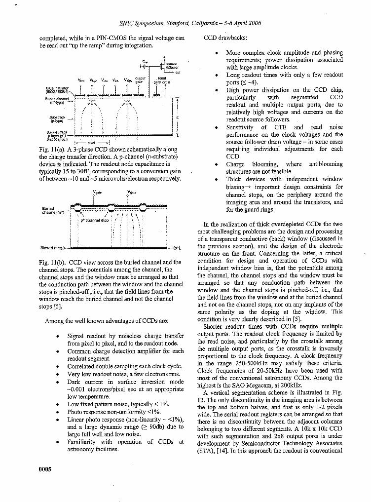
3. THICK OVERDEPLETED SENSORS AND THE NEED FOR A BIASED CONDUCTIVE WINDOW
It is a well established practice that silicon detectors for x-rays and charged particles are designed in a configuration p+-n, or p-n’, that is, a junction contact for electrodes (strips or pixels) on a high resistivity substrate, and an “ohmic contact” (a thin higher doping of the same polarity as the substrate). They are usually operated with a high enough voltage between the two contacts to achieve overdepletion. The thickness of the ohmic contact window is not of concern in most applications of such detectors. Where it becomes of concern, e.g., for soft x-rays and low energy charged particles, it is rarely to the extreme as is the case for detection of photons in the near-UV part of the spectrum, where the absorption length decreases to a few nanometers, Fig.3.
In conventional CCDs for astronomy the p-n structures are confined to the “front’), that is, the electrode side of the sensor. The substrate is not fully depleted and there is no bias applied to the “back”, that is, the window. A very effective window treatment for p-substrate (n-channel) CCDs was developed by Lesser [5 ] , where the surface is charged negatively by a few tenths of a volt. This forces the electrons due to photons converted veiy near the surface to drift into the field free region, from which they diffuse into the depletion region, and then drift to potential wells in the buried channel. This method has produced probably the best results in quantum efficiency at short wavelengths. However, this method does not allow the window to be biased, and the substrate cannot be overdepleted.
Overdepletion requires a high electric field over almost all of the charge carrier path, while (at the very beginning of the carrier path) the field has to be reduced to zero before reaching the window surface leaving a very thin conductive layer. This is illustrated schematically in Fig.10, and it requires a very shallow but highly dopedlayer. The surface sheet-doping-density has to exceed the displacement charge density EE corresponding to the electric field at the boundary of the high resistivity substrate and the highly doped layer at the window. This presents some very challenging processing problems. The work on the window processing as applied to CCDs has been reviewed in [5]. The high temperature annealing process of a doped polysilicon window has produced very good results [3]. This process requires metal deposition on the front to be
performed after annealing, if aluminum is used. The processing of the thinned wafer has to be done before attaching the die to the support substrate, and this poses a lower limit to the sensor thickness (somewhere between 150 and 200 microns). To get around this limitation, low temperature methods have been, or are being developed. Ion implantation followed by laser annealing has been used at Lincoln Laboratory and at e2v, [5], [6]. A method using molecular beam epitaxy called “delta doping” has been under development [13].
There has been no information on window processing in PIN-CMOS sensors in published reports. The results on QE published by RSC and RVS, and about their devices, indicate that successful (proprietary) methods for window processing in thick overdepleted PIN sensors have been developed [8], [9], [lo], [ll].
E E = q N h e
\ J E -3kV/cm - \ I
/ I /- 1pi , ~ * ~ I o n m ,
N-10‘g/cm3 N-1012/cm*2 - 5-10 kohmcm
I I I I
Fig.10. An illustration of the termination of the electric field at the window of an overdepleted sensor. A highly doped layer at the window is required to bring the electric field to zero before it can reach the surface, and to leave a thin conductive layer at the surface.
4. DEVELOPMENTS IN CHARGE COUPLED DEVICES (CCDS)
The CCD principle is shown schematically in Figs. 1 1 (a) and 11 (b). A unique feature of the CCD concept is that the signal charge is transferred serially by a noiseless process (very high CTE) to a single sense node, where it is converted to a signal voltage, while in a PIN CMOS sensor, the charge to voltage conversion takes place in parallel at the sense node of each pixel. In a CCD the pixels are read out after the integration is
0005
t
SNIC Symposium, Stanford, California - 3-6 April 2006
completed, while in a PIN-CMOS the signal voltage can be read out "up the ramp" during integration.
+
Fig. 11 (a). A 3-phase CCD shown schematically along the charge transfer direction. A p-channel (n-substrate) device is indicated. The readout node capacitance is typically 15 to 30fF, corresponding to a conversion gain of between -1 0 and -5 microvolts/electron respectively.
Fig. 1 l(b). CCD view across the buried channel and the channel stops. The potentials among the channel, the channel stops and the window must be arranged so that the conduction path between the window and the channel stops is pinched-off , i.e., that the field lines from the window reach the buried channel and not the channel stops [5].
Among the well known advantages of CCDs are:
Signal readout by noiseless charge transfer from pixel to pixel, and to the readout node. Common charge detection amplifier for each readout segment. Correlated double sampling each clock cycle. Very low readout noise, a few electrons rms. Dark current in surface inversion mode -0.001 electrons/pixel sec at an appropriate low temperature. Low fixed pattern noise, typically < 1%. Photo response non-uniformity 4%. Linear photo response (non-linearity - <1%), and a large dynamic range (2 9Odb) due to large full well and low noise. Familiarity with operation of CCDs at astronomy facilities.
CCD drawbacks:
More complex clock amplitude and phasing requirements; power dissipation associated with large amplitude clocks. Long readout times with only a few readout
High power dissipation on the CCD chip, particularly with segmented CCD readout and multiple output ports, due to relatively high voltages and currents on the readout source followers. Sensitivity of CTE and read noise perfomiance on the clock voltages and the source follower drain voltage - in some cases requiring individual adjustments for each CCD. Charge blooming, where antiblooining structures are not feasible Thick devices with independent window biasing+ important design constraints for channel stops, on the periphery around the imaging area and around the transistors, and for the guard rings.
ports (5 -4).
In the realization of thick overdepleted CCDs the two most challenging problems are the design and processing of a transparent conductive (back) window (discussed in the previous section), and the design of the electrode structure on the front. Concerning the latter, a critical condition for design and operation of CCDs with independent window bias is, that the potentials among the channel, the channel stops and the window must be arranged so that any conduction path between the window and the channel stops is pinched-off, i.e., that the field lines from the window end at the buried channel and not on the channel stops, nor on any implants of the same polarity as the doping at the window. This condition is very clearly described in [5].
Shorter readout times with CCDs require multiple output ports. The readout clock frequency is limited by the read noise, and particularly by the crosstalk among the multiple output ports, as the crosstalk is inversely proportional to the clock frequency. A clock frequency in the range 250-5OOkHz may satisfy these criteria. Clock frequencies of 20-5OkHz have been used with most of the conventional astronomy CCDs. Among the highest is the SA0 Megacam, at 200kHz.
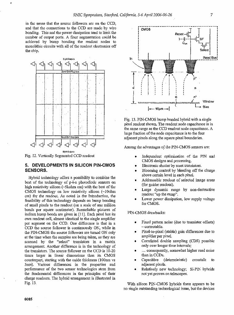
A vertical segmentation scheme is illustrated in Fig. 12. The only discontinuity in the imaging area is between the top and bottom halves, and that is only 1-2 pixels wide. The serial readout registers can be arranged so that there is no discontinuity between the adjacent columns belonging to two different segments. A 10k x 10k CCD with such segmentation and 2x8 output ports is under development by Semiconductor Technology Associates (STA), [14]. In this approach the readout is conventional
0005
. c
~ ~~~~ ~
SNIC Symposium, Stanford, California, 3-6 April 2006-06-26 7
in the sense that the source followers are on the CCD, and that the connections to the CCD are made by wire bonding. This and the power dissipation tend to limit the number of output ports. A fiier segmentation could be achieved by bump bonding the readout nodes to monolithic circuits with all of the readout electronics off the chip.
<
< Elgiil OulpUh
Fig. 12. Vertically Segmented CCD readout
5. DEVELOPMENTS IN SILICON PIN-CMOS SENSORS.
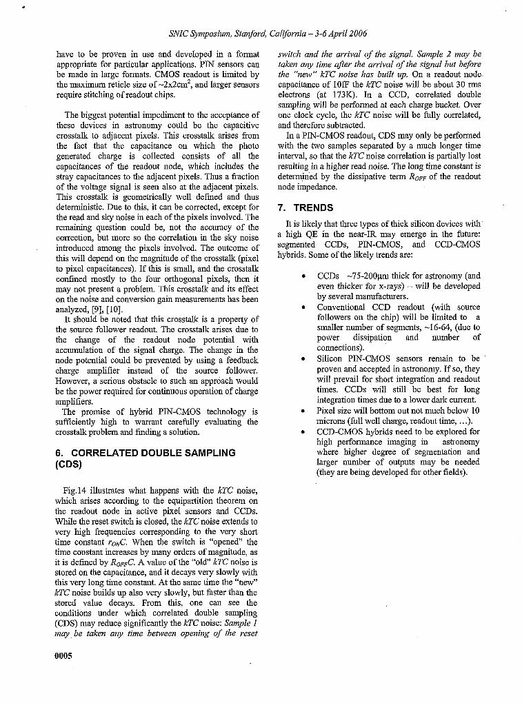
Hybrid technology offers a possibility to combine the best of the technology of p-i-n photodiode sensors on high resistivity silicon (-5kohm cm) with the best of the CMOS technology on low resistivity silicon (-1Oohm cm) for the readout. As noted in the Introduction, the feasibility of this technology depends on bump bonding of small pixels to the readout (on a scale of one million bonds per square centimeter). Remarkable pictures of indium bump bonds are given in [ 111. Each pixel has its own readout cell, almost identical to the single amplifier per segment on the CCD. One difference is that in a CCD the source follower is continuously ON, while in the PIN-CMOS the source followers are turned ON only at the time when the samples are being taken, as they are scanned by the “select” transistors in a matrix arrangement. Another difference is in the technology of the transistors. The source follower on the CCD is 10-20 times larger in linear dimensions than its CMOS counterpart, starting with the oxide thickness (1 OOnm vs 5nm). Various differences in the properties and performance of the two sensor technologies stem from the fundamental differences in the principles of their charge readouts. The hybrid arrangement is illustrated in Fig. 13.
Fig. 13. PIN-CMOS bump bonded hybrid with a single pixel readout shown. The readout node capacitance is in the same range as the CCD readout node capacitance. A large fraction of the node capacitance is to the four adjacent pixels along the square pixel boundaries.
Among the advantages ofthe PIN-CMOS sensors are:
Independent optimization of the PIN an CMOS designs and processing. Electronic shutter by reset transistors. Blooming control by bleeding off the charge above certain level in each pixel. Addressable readout of selected image areas (for guider readout). Large dynamic range by non-destructive readout “LIP the ramp”.
0 Lower power dissipation, low supply voltage for CMOS.
PIN-CMOS drawbacks:
Fixed pattern noise (due to transistor offsets) - correctable. Pixel-to-pixel (stable) gain differences due to amplifier per pixel. Correlated double sampling (CDS) possible only over longer time intervals; . . . consequently, somewhat higher read noise than in CCDs. Capacitive (deterministic) crosstalk to adjacent pixels. Relatively new technology; Si-PIN hybrids not yet proven on telescopes.
With silicon PIN-CMOS hybrids there appears to be no single outstanding technological issue, but the devices
0005
. b
SNIC Symposium, Stanford, California - 3-6 April 2006
have to be proven in use and developed in a format appropriate for particular applications. PIN sensors can be made in large formats. CMOS readout is limited by the maximum reticle size of -2x2cm2, and larger sensors require stitching of readout chips.
The biggest potential impediment to the acceptance of these devices in astronomy could be the capacitive crosstalk to adjacent pixels. This crosstalk arises from the fact that the capacitance on which the photo generated charge is collected consists of all the capacitances of the readout node, which includes the stray capacitances to the adjacent pixels. Thus a fraction of the voltage signal is seen also at the adjacent pixels. This crosstalk is geometrically well defined and thus deterministic. Due to this, it can be corrected, except for the re3d and sky noise in each of the pixels involved. The remaining question could be, not the accuracy of the correction, but more so the correlation in the sky noise introduced among the pixels involved. The outcome of this will depend on the magnitude of the crosstalk (pixel to pixel capacitances). If this is small, and the crosstalk confined mostly to the four orthogonal pixels, then it may not present a problem. This crosstalk and its effect on the noise and conversion gain measurements has been analyzed, [9], [lo].
It should be noted that this crosstalk is a property of the source follower readout. The crosstalk arises due to the change of the readout node potential with accumulation of the signal charge. The change in the node potential could be prevented by using a feedback charge amplifier instead of the source follower. However, a serious obstacle to such an approach would be the power required for continuous operation of charge amplifiers.
The promise of hybrid PIN-CMOS technology is sufficiently high to warrant carefully evaluating the crosstalk problem and finding a solution.
6. CORRELATED DOUBLE SAMPLING (CDS)
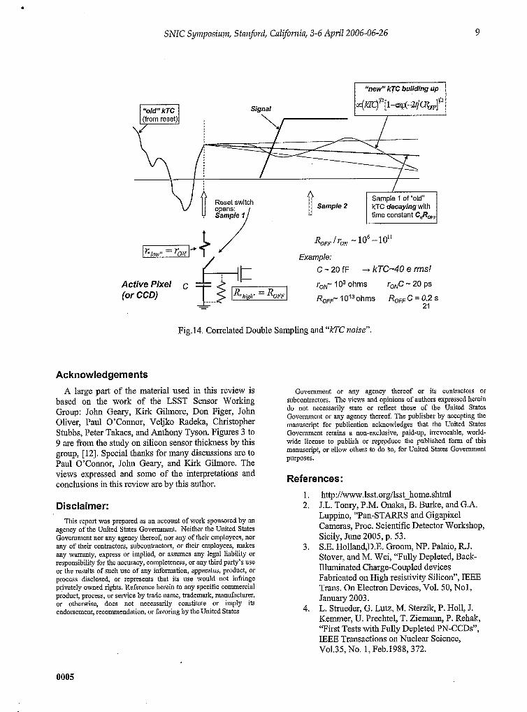
Fig. 14 illustrates what happens with the kTC noise, which arises according to the equipartition theorem on the readout node in active pixel sensors and CCDs. While the reset switch is closed, the lcTC noise extends to very high frequencies corresponding to the very short time constant r ~ g . When the switch is “opened” the time constant increases by many orders of magnitude, as it is defined by R O F F C . A value of the “old” kTC noise is stored on the capacitance, and it decays very slowly with this very long time constant. At the same time the “new” kTC noise builds up also very slowly, but faster than the stored value decays. From this, one can see the conditions under which correlated double sampling (CDS) may reduce significantly the kTC noise: Sample 1 may, be taken any time between opening of the reset
switch and the arrival of the signal. Sample 2 may be taken any tiine after the arrival of the signal but before the “new” kTC noise has built up. On a readout node., capacitance of lOfF the kTC noise will be about 30 rms electrons (at 173K). In a CCD, correlated double sampling will be performed at each charge bucket. Over one clock cycle, the kTC noise will be fully correlated, and therefore subtracted.
In a PIN-CMOS readout, CDS may only be performed with the two samples separated by a much longer time interval, so that the kTC noise correlation is partially lost resulting in a higher read noise. The long time constant is determined by the dissipative term ROFF of the readout node impedance.
7. TRENDS It is likely that three types of thick silicon devices witk
a high QE in the near-IR may emerge in the future: segmented CCDs, PIN-CMOS, and CCD-CMOS hybrids. Some of the likely trends are:
CCDs -75-2OOpm thick for astronomy (and even thicker for x-rays) - will be developed by several manufacturers. Conventional CCD readout (with source followers on the chip) will be limited to a smaller number of segments, -16-64, (due to power dissipation and number of connections). Silicon PIN-CMOS sensors remain to be proven and accepted in astronomy. If so, they will prevail for short integration and readout times. CCDs will still be best for long integration times due to a lower dark current. Pixel size wiII bottom out not much below 10 microns (full well charge, readout time, . . .). CCD-CMOS hybrids need to be explored for high performance imaging in astronomy where higher degree of segmentation and larger number of outputs may be needed (they are being developed for other fields).
0005
. c
SNIC Synzposiuvz, Stanford, Calfomia, 3-6 April 2006-06-26 9
“new” kTC building up
Signal
Samp[e 1 of “old kTC decayingwith
/
RoFFIyoN -1O6-10”
Example: c - 20 fF
roN- 1 O3 ohms
R o F r 10130hms
-, kTC-40 e rms! ro,C - 20 ps ROFFC = 0.2 s
21
Active Pixel c L-IL (or CCD) 1-2 pG=q
- -
Fig.14. Correlated Double Sampling and “kTC noise”.
Acknowledgements A large part of the material used in this review is
based on the work of the LSST Sensor Working Group: John Geary, Kirk Gilmore, Don Figer, John Oliver, Paul O’Connor, Veljko Radeka, Christopher Stubbs, Peter Takacs, and Anthony Tyson. Figures 3 to 9 are from the study on silicon sensor thickness by this group, [12]. Special thanks for many discussions are to Paul O’Connor, John Geary, and Kirk Gilmore. The views expressed and some of the interpretations and conclusions in this review are by this author.
Disclaimer: This report was prepared as an account of work sponsored by an
agency of the United States Government. Neither the United States Government nor any agency thereof, nor any of their employees, nor any of their contractors, subcontractors, or their employees, makes any warranty, express or implied, or assumes any legal liability or responsibility for the accuracy, completeness, or any third party’s use or the results of such use of any information, apparatus, product, or process disclosed, or represents that its use would not infringe privately owned rights. Reference herein to any specific commercial product, process, or service by trade name, trademark, manufacturer, or otherwise, does not necessarily constitute or imply its endorsement, recommendation, or favoring by the United States
Government or any agency thereof or its contractors or subcontractors, The views and opinions of authors expressed herein do not necessarily state or reflect those of the United States Government or any agency thereof. The publisher by accepting the manuscript for publication acknowledges that the United States Government retains a non-exclusive, paid-up, irrevocable, world- wide license to publish or reproduce the published form of this manuscript, or allow others to do So, for United States Government purposes.
References: http://www.lsst.org/lsst-home.shtm1 J.L. Tonry, P.M. Onaka, B. Burke, and G.A. Luppino, “Pan-STARRS and Gigapixel Cameras, Proc. Scientific Detector Workshop, Sicily, June 2005, p. 53. S.E. Holland,D.E. Groom, NP. Palaio, R.J. Stover, and M. Wei, “Fully Depleted, Back- Illuminated Charge-Coupled devices Fabricated on High resistivity Silicon”, IEEE Trans. On Electron Devices, Vol. 50, No1 , January 2003. L. Strueder, G. Lutz, M. Sterzik, P. Holl, J. Kemmer, U. Prechtel, T. Ziemann, P. Rehak, “First Tests with Fully Depleted PN-CCDs”, IEEE Transactions on Nuclear Science, Vo1.35, No. 1, Feb.1988,372.
0005
4
? r
SNIC Symposium, Stanford, California - 3-6 April 2006
5. B.E. Burke, J.A. Gregory, A.H. Loomis, M. Lesser, M.W. Bautz, S.E. Kissel, D.D. Rathman, R.M. Osgood III, M.J. Cooper, T.A. Lind, and G.R. Ricker, “CCD Soft-X-Ray detectors with Improved High- and Low- energy Performance”, IEEE Trans. On Nucl. Sci., Vol. 51, No. 5, Part 1, Oct. 2004, p. 2322.
6. P. Jorden, K. Ball, R. Bell, D. Burt, N. Guyatt, K. Hadfield, P. Jerram, P. Pool, A. Pike, A. Holland, N. Murray, “Commercialization of Full Depletion Scientific CCDs”, Proc. SPIE Astronomical Telescopes and Instrumentation, 24-31 May 2006, [6276-041. Y. Kamata, S. Miyazaki, H. Tsunemi, T. G. Tsuru, S. Tagaki, K. Miyaguchi, M. Muramatsu, H. Suzuki, “Recent Results of the Fully-depleted Back-illuminated CCD Developed by Hamamatsu”, Proc. SPIE Astronomical Telescopes and Instrumentation, 24-31 May 2006, [6276-731.
8. A. Hoffman, M. Loose, and V. Suntliaralingam, “CMOS Detector Technology”, Proc. Scientific Detector Workshop, Sicily, June 2005, p. 377. G. Finger, R. J. Dorn, S. Eschbaumer, L. Mehrgan, M. Meyer, A. F. M. Moorwood, J. Stegmeier, “Interpixel Capacitance in Large Format CMOS Hybrid Arrays”, Proc. SPIE Astronomical Telescopes and Instrumentation, 24-31 May 2006, [6276-161.
Evaluating Hybridized Silicon PIN Arrays”, Proc. Scientific Detector Workshop, Sicily, June 2005.
Harris, J.-G. Shin, J. J. Cantrell, “Enabling Technologies for Large Hybrid Focal Plane Arrays with Small pixels”, Raytheon vision Systems, Feb. 2006.
Geary, D.K. Gilmore, J. Oliver, C.W. Stubbs, P.Z. Takacs, J.A. Tyson, “Study of Silicon Thickness Optimization for LSST”, Proc. SPIE Astronomical Telescopes and Instrumentation, 24-3 1 May 2006, [6276-751.
13. B. Burke, P. Jorden, and P. Vu, “CCD Technology”, Proc. Scientific Detector Workshop, Sicily, June 2005, p.225.
14. S. Nikzad, J. Blacksberg, M.E. Hoenk, S.T. Elliot, “Delta-doped High Purity Silicon CCDs with High QE from UV to NIR for SNAP an ORION Missions”, Proc. SPIE Astronomical Telescopes and Instrumentation, 24-31 May 2006, [6276-131.
lOkxlOk CCD, STA 1600.
7.
9.
10. A. Moore, “Operating, Testing, and
I
11. K. T. Veeder, R. Ajer, R. Salafian, M. R.
12. P. O’Connor, V. Radeka, D. Figer, J.G.
15. Semiconductor Technology Associates, Inc,
0005