Embed Size (px)
Citation preview

CCD or CMOS: can CMOS sensors replace CCDs in all cases?
CMOS sensors are on the march, replacing CCD sensors in many places. However, both technologies have their own specific advantages and disadvantages. In the end, which sensor is best suited for which use to fulfill the demands placed on it depends upon the objective and the general conditions of the application.
When Sony announced they were discontinuing their CCD sensors, the news gen-erated many questions. In the field of industrial imaging, users have come to value CCD sensors over the course of many years, primarily due to their advantageous image quality as well as the outstanding Global Shutter functionality. The fact that Sony, among the foremost imaging sensor manufacturers, is now focusing on CMOS sensor technology could indicate that it has been developed so far that the majority of applications can be served with CMOS sensors.
WHITE PAPER

In the following paper, commonalities and differences of CCD and CMOS sensors will be analyzed in seeking an answer to the question whether CCD sensors can generally be replaced in the future by CMOS sensors without restriction.
CCD and CMOS: sensor technology for the visible spectral rangeCCD and CMOS sensors belong to quantum detectors. Both technologies are based on silicon, the semiconductor material, and are sensitive in the same spec-tral range from approximately 300 to 1000 nm.
But in what ways do the two technologies differ? The principal difference lies in the semiconductor element where the charge is converted into voltage. In a CCD sensor, a vertical and horizontal charge transport first takes place. The serial charge/voltage conversion of all pixels takes place outside the sensor in the cam-era’s electronics. All pixel charges are converted via an output outside the sensor to an analog voltage.
Image 1: optical sensors and the electromagnetic spectrum
Partial range of the electromagnetic spectrum

Image 2: principle of the interline transfer CCD as well as of the CMOS sensor
In contrast, the charge/voltage conversion in CMOS sensors occurs in every pixel on the sensor. Corresponding to the activated line, the signal is amplified via the readout circuit, noise-minimized and digitized, and finally transmitted in parallel via a configurable number of LVDS (Low Voltage Differential Signaling) wires.
CCD sensor advantages and disadvantagesIn a CCD sensor, all pixel charges are converted via an output to an analog volt-age, amplified and digitized. In doing so, a high quality image with high pixel ho-mogeneity, very uniform signal with low fixed pattern noise and usually low dark current, is achieved.
Furthermore, CCDs achieve high sensitivity as well as good signal quality in low light conditions due to the higher fill factor (relationship of the photosensitive area to the entire pixel area).
Another advantage lies in the perfect Global Shutter, i.e., the concurrent illumi-nation of all pixels. For this reason, CCDs are well suited for use in machine vision applications, especially those requiring very short exposure times.
One disadvantage to CCD sensors lies in the limited readout speed of the serial data stream. Therefore, modern CCDs with higher resolutions are commonly manufactured in multi-tap technologies (division of the sensor into several image areas) in order to achieve the n-fold readout speed vis-à-vis single-tap sensors.
A/D conversion outside of the sensor A/D conversion in the sensor

However, this has the disadvantage that a signal adjustment (gain offset correc-tion) of the tap becomes necessary, as even the slightest deviations lead to visible differences at the limit of the tap.
Another disadvantage to CCD sensors is that charges which exceed the full well capacity of the pixel cell impinge into neighboring pixels. This becomes visible in typical blooming effects. The only remedy is a reduction of the occurring amount of light. Moreover, during the readout of a serial charge transport in the vertical shift register, impinging photons can produce additional charge carriers – re-sulting in so-called smearing. Smearing can be prevented by using a mechanical shutter in front of the sensor or by using flash lighting.
Advantages and disadvantages of CMOS sensorsIn a CMOS sensor, the charge/voltage conversion takes place in each pixel and the image information is converted to digital information on the CMOS sensor chip. This type of function requires an elevated design complexity. More complex CMOS designs with Global Shutter and CDS (Correlated Double Sampling) to reduce fixed pattern noise are based on pixel cells with 5 to 8 transistors and thus reduce the light-sensitive area per pixel. Every column/pixel possesses an amplifi-er that works independently of the others. Due to deviations caused by the tech-nology used, disparities arise in the uniformity between the pixels of the individual columns, which again leads to increased fixed pattern noise.
For applications with moving objects, a Global Shutter sensor function is neces-sary. This requires the CMOS sensor to contain a storage area in the pixel that is protected from light as much as possible. In practice, this is not successful in older CMOS designs – the area is more or less light sensitive and demonstrates a par-
Image 3: on the left, CCD blooming and smearing artifacts; on the right, CMOS sensor without these artifacts
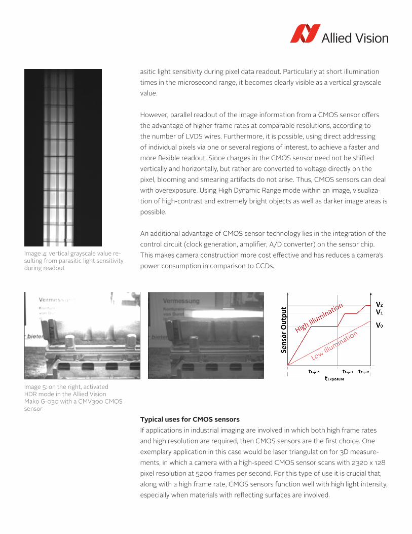
Image 5: on the right, activated HDR mode in the Allied Vision Mako G-030 with a CMV300 CMOS sensor
Image 4: vertical grayscale value re-sulting from parasitic light sensitivity during readout
asitic light sensitivity during pixel data readout. Particularly at short illumination times in the microsecond range, it becomes clearly visible as a vertical grayscale value.
However, parallel readout of the image information from a CMOS sensor offers the advantage of higher frame rates at comparable resolutions, according to the number of LVDS wires. Furthermore, it is possible, using direct addressing of individual pixels via one or several regions of interest, to achieve a faster and more flexible readout. Since charges in the CMOS sensor need not be shifted vertically and horizontally, but rather are converted to voltage directly on the pixel, blooming and smearing artifacts do not arise. Thus, CMOS sensors can deal with overexposure. Using High Dynamic Range mode within an image, visualiza-tion of high-contrast and extremely bright objects as well as darker image areas is possible. An additional advantage of CMOS sensor technology lies in the integration of the control circuit (clock generation, amplifier, A/D converter) on the sensor chip. This makes camera construction more cost effective and has reduces a camera’s power consumption in comparison to CCDs.
Typical uses for CMOS sensorsIf applications in industrial imaging are involved in which both high frame rates and high resolution are required, then CMOS sensors are the first choice. One exemplary application in this case would be laser triangulation for 3D measure-ments, in which a camera with a high-speed CMOS sensor scans with 2320 x 128 pixel resolution at 5200 frames per second. For this type of use it is crucial that, along with a high frame rate, CMOS sensors function well with high light intensity, especially when materials with reflecting surfaces are involved.

Image 6: laser triangulation for 3D measurements of structural beam In recent years, CMOS technology has demonstrated clear advances in image
quality along with the advantage of high frame rates. Manufacturers such as Sony, CMOSIS, e2V, On Semi and others were able to markedly improve their CMOS designs. Modern CMOS sensors with Global Shutter are available in different res-olutions and with high frame rates, such as sensors with more than 500 frames per second at VGA resolution. By reducing the dark and fixed pattern noise as well as raising the quantum efficiency, these sensors deliver good image quality even in low light conditions.
The memory’s parasitic light sensitivity during readout has been reduced mark-edly. The result is an improved Global Shutter efficiency with values in the range of 10000:1 or better. As such, modern CMOS sensors are well-suited for appli-cations with moving objects. At an estimated readout time of 10 ms (at 100 fps), parasitic light sensitivity would amount to just 1 µs, which is not critical for most use cases with moving objects.
Sony’s Exmor and Exmor R sensor technologies, with PregiusTM and StarvisTM CMOS pixel architectures, are leading the way. PregiusTM is optimized for the demands of industrial imaging Global Shutter pixel technology, which, based on Sony’s CCD pixel technology, possesses a shielded analog memory that protects the generated charges from undesirable parasitic light and guarantees a perfect Global Shutter. One analog CDS layer before, as well as an additional CDS layer after the analog/digital conversion effects a dual noise suppression, whereby the readout and fixed pattern noise are held to a minimum. Thus, images with short illumination times and, therefore, smaller motion blurs of rapidly moving objects are possible.

The Sony IMX 174 is representative of this technology, with a full well capacity of over 30,000 electrons and a dynamic range over 70 db, as well as single-digit values in readout noise.
Continuing developments of PregiusTM technology with a further reduction in pixel design demonstrate minimal readout noise. Moreover, a thicker silicon epi-taxial layer on the photodiode leads to increased sensitivity in the near-infrared spectral range.
Thus, modern CMOS sensors are suited for industrial imaging applications as well as for outdoor applications with high light contrasts in the areas of security and intelligent transportation systems.
Applications in which CCD sensors continue to be usedDue to their very homogenous image quality with low fixed pattern noise, CCD sensors have advantages for medical and scientific applications, particularly for fluorescence microscopy and high-resolution microscopy. For application fields requiring very high resolution, such as aerial mapping, CCD sensors are also well suited. Furthermore, CCDs offer advantages for applications with long exposure times, such as applications in astronomy, due to minimal dark current.
Manufacturers such as OnSemi, Sharp and e2v, for example, are continuing to develop CCD technology and are offering special CCD sensors with higher reso-lution, i.e., 50 MP, and higher sensitivity, for demanding applications in the field of science, especially for metrology applications, for which high image homogeneity at high resolution is required.
Special CCD sensors, such as EMCCDs (Electron Multiplication CCD) with very high dynamic range, are optimized for recording images in day- and night light, for applications with extremely little light or for applications such as molecular and cellular examination.
CDD design improvements are optimized microlens configurations, special epi-taxy doping and an increase of substrate thickness to improve sensitivity in the visible and the NIR range.

ConclusionAlongside resolution, frame rate and image quality, cost requirements play a role in the selection of sensors. As a result of the existing advantages with regard to frame rate, and the improvements listed earlier in image quality, combined with improved Global Shutter efficiency, a clear trend is emerging to implement CMOS sensors more and more often as an alternative to CCDs in industrial imaging applications.
However, there are still special applications, as described above, for which current CCD sensors offer advantages in comparison to CMOS sensors.
Image 7: Applications using CCD cameras (fluorescence microsco-py, high-resolution microscopy, astronomy, aerial mapping)