Embed Size (px)
Citation preview

CCS Technical DocumentationNHL-2NA Series Transceivers
Issue 1 07/02 Nokia Corporation
System Module LG4 and Grip Module LS4

NHL-2NASystem Module LG4 and Grip Module LS4 CCS Technical Documentation
This page intentionally left blank.
Page 2 Nokia Corporation Issue 1 07/02

CCS Technical Documentation System Module LG4 and Grip Module LS4NHL-2NA
Table of ContentsPage No
Abbreviations ................................................................................................................. 6LG4 System Module ...................................................................................................... 8
Introduction ................................................................................................................8Technical overview ........................................................................................................ 8
LG4 features ................................................................................................................8Component placement and PWB outline .....................................................................8
Block diagram .............................................................................................................. 12UI Interface ................................................................................................................12
Baseband Technical Summary..................................................................................... 13Functional Description................................................................................................. 14
BB Description ..........................................................................................................14Memory Configuration............................................................................................ 14Energy Management ............................................................................................... 14
Modes of Operation ...................................................................................................15Voltage limits .......................................................................................................... 15
Clocking Scheme .......................................................................................................16UPP_WD2 voltage/clock frequency adjusting........................................................ 16
Power Distribution, Control and Reset ......................................................................17Power-up sequence (Reset mode) ........................................................................... 18Powering off ............................................................................................................ 18Controlled powering off .......................................................................................... 18Uncontrolled powering off ...................................................................................... 18Watchdogs............................................................................................................... 18Charging .................................................................................................................. 19Chargers .................................................................................................................. 19Battery ..................................................................................................................... 19
Back-up battery and real time clock ..........................................................................20Baseband Measurement A/D Converter ....................................................................20
NHL-2NA BB Features & HW interfaces ................................................................... 21NHL-2NA BB User interface ....................................................................................21
UI-Module Interface................................................................................................ 21Power Key ............................................................................................................... 21Grip Interface .......................................................................................................... 21
Bluetooth ....................................................................................................................23IR ...............................................................................................................................23SIM Interface .............................................................................................................23NHL-2NA Audio Concept .........................................................................................24
Earpiece................................................................................................................... 24Microphone ............................................................................................................. 25IHF Amplifier and Speaker ..................................................................................... 25External Audio interface ......................................................................................... 26
Camera Interface ........................................................................................................26Proximity Sensor .......................................................................................................27Proximity Detector components ................................................................................28
Lightguides.............................................................................................................. 28IRED........................................................................................................................ 28Photodiode............................................................................................................... 28
Issue 1 07/02 Nokia Corporation Page 3

NHL-2NASystem Module LG4 and Grip Module LS4 CCS Technical Documentation
HW Implementation................................................................................................ 28Ambient Light Sensor ................................................................................................30Flashing ......................................................................................................................31
Connections to Baseband ........................................................................................ 31Testing interfaces .......................................................................................................32 Extreme Voltages ......................................................................................................33Temperature Conditions ............................................................................................33Humidity and Water Resistance ................................................................................33RF Module .................................................................................................................34
Functional block descriptions.................................................................................. 34The Frequency synthesizer...................................................................................... 34RF Frequency Plan .................................................................................................. 36DC characteristics ................................................................................................... 37Regulators................................................................................................................ 37Power Distribution Diagram ................................................................................... 38RF characteristics .................................................................................................... 39RF Block Diagram .................................................................................................. 40
Voltage Supplies and References ..............................................................................41Receiver .....................................................................................................................43Transmitter .................................................................................................................44
AGC strategy........................................................................................................... 45AFC function........................................................................................................... 47DC-compensation.................................................................................................... 48Power control with analog temperature compensation scheme .............................. 48
Grip Module................................................................................................................. 50Abbreviations .............................................................................................................50Introduction ................................................................................................................50General Interface between Grip and Transceiver ......................................................53Grip Keyboard ...........................................................................................................56
Electrical implementation ....................................................................................... 56Unit limits................................................................................................................ 57
Vibra ..........................................................................................................................57Electrical interface .....................................................................................................57Current Gauge ............................................................................................................59
Interfacing the current gauge................................................................................... 59Backlight ....................................................................................................................61
Electrical interface................................................................................................... 61Hall Sensor and Magnet .............................................................................................62
Magnet..................................................................................................................... 62DC Jack and Battery Connector ................................................................................63
Electrical interface................................................................................................... 63
Table of Schematic DiagramsPage No
RF-BB connection diagram 1Accessories interface diagaram 2AEM diagram 3Baseband Diagram 4BB-RF Interface diagram 5
Page 4 Nokia Corporation Issue 1 07/02

CCS Technical Documentation System Module LG4 and Grip Module LS4NHL-2NA
SIM card interface diagram 6CPU Diagram 7IR module diagram 8LPRF diagram 9Memories diagram 10Power Diagram 11RF Diagram 12Test Interface 13UEM Diagram 14User Interface Diagram 15Parts Placement Diagram LG4_07 16
Issue 1 07/02 Nokia Corporation Page 5

NHL-2NASystem Module LG4 and Grip Module LS4 CCS Technical Documentation
AbbreviationsADC Analog-Digital ConverterAEM Auxiliary Energy Management ASICAFC Automatic Frequency ControlALG Ambient Light GuideALS Ambient Light SensorARM Processor architectureASIC Application Specific Integrated CircuitBB BasebandBLUETOOTH, BT BluetoothBSI Battery Size IndicatorCBus Control Bus connecting UPP_WD2 with AEM and UEMCCI Camera Control InterfaceCCP Compact Camera PortCMT Cellular Mobile Telephone (MCU and DSP)CPU Central Processing UnitCSP Chip Scale PackageCTSI Clocking Timing Sleep Interrupt DAC Digital-Analog ConverterDAI Digital Audio InterfaceDBUS Data Bus DCN Offset Cancellation contol signalDIF Display InterFaceDLL Dynamic Link LibraryDRC Dynamic Range ControllerDSP Digital Signal ProcessorEFR Enhanced Full RateEGSM Extended – GSMEQ EqualizerEXT RF External RFGPRS General Packet Radio ServiceGSM Groupe Special Mobile/Global system mobileHF Hands freeHFCM Handsfree Common HS HandsetHSCSD High Speed Circuit Switched DataI/O Input/OutputIHF Integrated hands freeIC Integrated CircuitIR Infra redIRED InfraRed Emitting DiodeIrDA Infrared AssociationLCD Liquid Crystal DisplayLG4 NHL-2NA Main PWB moduleLNA Low Noise Amplifier MCU Micro Controller UnitMIC, mic MicrophonePA Transmit Power Amplifier
Page 6 Nokia Corporation Issue 1 07/02

CCS Technical Documentation System Module LG4 and Grip Module LS4NHL-2NA
PC Personal ComputerPDA Pocket Data ApplicationPWB Printed Wiring BoardRF Radio FrequencyRFBUS Control Bus For RF SDRAM Synchronous Dynamic Random Access MemorySIM Subscriber Identity ModuleUI User InterfaceUEM Universal Enefry ManagementVGA Video Graphic ArrayVCXO Voltage Controlled Crystal OscillatorVCTCXO Voltage Controlled Temperature Compensated Crystal Oscillator.VCM Voltage Controlled Module VGA Video Graphics Array
Issue 1 07/02 Nokia Corporation Page 7

NHL-2NASystem Module LG4 and Grip Module LS4 CCS Technical Documentation
LG4 System Module
IntroductionThis is the module specification of LG4 which is the main electronics module in NHL-2NAGSM dual band phone. NHL-2NA phone is also nick named as Nokia 7650. The salesname is Nokia 7650.
Technical overview
LG4 features• Dual band GSM tranceiver. EGSM900 and GSM1800 bands with GPRS class 6 and
HSCSD data capability• BB release is Galaxy WD2, main ASIC UPP_WD2• RF release is Gemini premium release for Lilly (but shrinked)• Bluetooth, based on BT102 module• IR, HW capable for 1Mbit data speed• Proximity sensor for controlling integrated handsfree feature (IHF)• Handsfree, headset and earpiece audio connections• VGA camera module connected with spring connector to LG4• Ambient light sensor for controlling display and keyboard backlights• Color display interface• Flex cable interface to LS4 Grip module
Component placement and PWB outlineComponents are placed only on one side of the LG4 module.
Figure 1 shows LG4 module from component side, main components are listed.
Page 8 Nokia Corporation Issue 1 07/02

CCS Technical Documentation System Module LG4 and Grip Module LS4NHL-2NA
Figure 1: Main components on LG4
Ambient light sensor
Antenna switch PA
Hagar VCO
UI module backlight DC/DC converter
UEM
UI module connector
AEM
IR Module
Earpiece connector
Proximity sensor
Bluetooth module, BT102
VCTCXO 64Mbit SDRA
UPP_WD2 32 + 128 Mbit flashes
Issue 1 07/02 Nokia Corporation Page 9

NHL-2NASystem Module LG4 and Grip Module LS4 CCS Technical Documentation
Figure 2: Spring connection pads on top side of LG4
Figure 3: Spring connection pads on back side of LG4 and flex cable solder pads
Power switch pads
Integrated handsfree speaker pads
Headset connector pads
BT antenna pads Microphone pads
Flex solder pads, Grip IF
Prod testing: Powering
Production testing
Camera pads
SIM GSM antenna pads
Page 10 Nokia Corporation Issue 1 07/02

CCS Technical Documentation System Module LG4 and Grip Module LS4NHL-2NA
Figure 4: Test points in LG4 baseband
Test points of BBJ140 (VBAtt) J262 (UEMRst)
J105 (AEMSleepX
J101 (Sleepclk)
J102 (SleepX)
J103 (PURX)
J100 (RFClk)
J138 (Vctrl (camera)
J270 (GenVbattIO)
J106 (SDRDa0)
J108 (SDRAMClk)
J07 (SDRAd0)
J115 (FlClk)
J111 (FLCS1x)
J109 (FLADa0)
J113 (FLCS0X)
J114 (FLDEX) (mem cntr)
J116 (TxID)J104 (UEMInt)
J120 (RxQD)
J117 (TxQD)
RF: J118 (AuXDA)
J119 (RxID)
J110 (VcoreA)
Issue 1 07/02 Nokia Corporation Page 11

NHL-2NASystem Module LG4 and Grip Module LS4 CCS Technical Documentation
Block diagramBelow is the block diagram of LG4 module. External interfaces are drawn as arrows cross-ing LG4 border.
Figure 5: Block diagram of LG4
UI InterfaceUI module interface pin numbering is presented in figure below. UI interface details are inUI-module specification.
Figure 6: UI connector pin numbering on LG4 side
LG4 module
BB
Bluetooth
RF
Sensors
Flashing & Testing Interface
Flex to LS4 (Grip)
VGA camera
UI-module
Audio SIM card
BT antenna
GSM antenna
Page 12 Nokia Corporation Issue 1 07/02

CCS Technical Documentation System Module LG4 and Grip Module LS4NHL-2NA
Baseband Technical SummaryThe heart of the BB is UPP_WD2, which includes MCU, DSP and Digital Control Logic.Powering handled by Using AEM ASIC and UEM ASIC. There is Flash Memory 128Mbit +32Mbit Flashes (20 Mbytes) and 64 Mbit (8 Mbytes) SDRAM. So there is a total of 28Mbytes of Memory Capacity.
In BB there is an integrated Handsfree Audio Amplifier In AEM. There are two Audio Ele-ments (Earpiece 8 mm and Speaker 16 mm) and External Galvanic Headset (DCT4) inter-face. IHF Speaker is also used to handle the Ringing tone. For IHF automated off functionthere is proximity Sensor. In NHL-2NA there is only one microphone for both modes HSand IHF.
For Data connectivity there is 1Mbit IR Module (IrDA compatible) and Bluetooth.
Display is MD-TFD type Color Display with 4096 Colors and 176x208 pixels with Back-light. Keyboard is partially in UI-Module and Partially in Grip-Module. Also there is ThisNavigation Key Feature in UI-Module.
For imaging purposes BB supports VGA camera via CCP interfaces, which are integratedin UPP_WD2.
Issue 1 07/02 Nokia Corporation Page 13

NHL-2NASystem Module LG4 and Grip Module LS4 CCS Technical Documentation
Functional Description
BB DescriptionCore is based on UPP_WD2 CPU, which is a special version of the DCT4 UPP ASIC.UPP_WD2 takes care of all the signal processing and operation controlling tasks of thephone as well as all PDA tasks.
For Power management there are two Asics for controlling energy management and sup-plying current and different voltages; UEM and AEM. UEM and SW have the main con-trol of the system voltages and operating modes and AEM acts as an auxiliary source ofvoltages and current. The main reset for the system is generated by the UEM.
The interface from the RF and audio sections is handled also by UEM. This ASIC providesA/D and D/A conversion of the in-phase and quadrature receive and transmit signalpaths and also A/D and D/A conversions of received and transmitted audio signals. Datatransmission between the UEM, AEM and RF and the UPP_WD2 is implemented usingdifferent serial connections (CBUS, DBUS and RFBUS). Digital speech processing is han-dled by UPP_WD2 ASIC. Internal HF with proximity sensor functionality is implementedinside the AEM ASIC.
A real time clock function is integrated into UEM, which utilizes the same 32kHz-clocksource as the sleep clock. A rechargeable battery provides backup power to run the RTCwhen the main battery is removed. Backuptime is 20 Hours.
Memory ConfigurationNHL-2NA uses two kinds of memories, Flash and SDRAM. These Memories have theirown Dedicated buses in UPP_WD2.
Synchronous DRAM is used as working memory. Interface is 16 bit wide data and 14 bitAddress. Memory clocking speed is 104 MHz. The SDRAM size 64Mbits (4Mx16).
SDRAM I/O is 1.8 V and core 2.78 V supplied by AEM’s regulators VIOA and VMEMA. Allmemory contents are lost if the supply voltage is switched off.
Multiplexed Flash Memory Interface is used to store the MCU program code and UserData. The memory interface is a burst type FLASH with multiplexed address/data bus.
Both I/O and core voltage are 1.8 V supplied by AEM’s VMEMB.
Energy ManagementThe master of EM control is UEM and with SW they have the main control of the systemvoltages and operating modes. AEM (Auxiliary Energy Management) acts as an auxiliarysource of voltages and current.
Page 14 Nokia Corporation Issue 1 07/02

CCS Technical Documentation System Module LG4 and Grip Module LS4NHL-2NA
Modes of OperationNHL-2NA employs several hardware & SW controlled operation modes. Main Modes aredescribed below.
• NO_SUPPLY mode means that the main battery is not present or itsvoltage is too low (below UEM master reset threshold) and back-up bat-tery voltage is too low.
• In BACK_UP mode the main battery is not present or its voltage is toolow but back-up battery has sufficient charge in it.
• In PWR_OFF mode the main battery is present and its voltage is overUEM master reset threshold. All regulators are disabled.
• RESET mode is a synonym for start-up sequence and contains in factseveral modes. In this mode regulators and oscillators are enabled andafter they have stabilized system reset is released and PWR_ON modeentered.
• In PWR_ON mode SW is running and controlling the system.
• SLEEP mode is entered from PWR_ON mode when the system’s activ-ity is low (SLEEPX and AEMSLEEPX controlled by SW).
• FLASHING mode is for production SW download.
Voltage limitsIn the following the voltage limits of the system are listed. These are also controlling sys-tem states.:
The master reset threshold controls the internal reset of UEM. If battery voltage is aboveVMSTR, UEM’s charging control logic is alive. Also, RTC is active and supplied from themain battery. Above VMSTR UEM allows the system to be powered on although this maynot succeed due to voltage drops during start-up. SW can also consider battery voltage
Parameter Description Value
VMSTR+ Master reset threshold (rising) 2.1 V (typ.)
VMSTR- Master reset threshold (falling) 1.9 V (typ.)
VCOFF+ Hardware cutoff (rising) 3.1 V (typ.)
VCOFF- Hardware cutoff (falling) 2.8 V (typ.)
V_BUCOFF+ Back-up battery cutoff (rising) 2.1 V (typ.)
V_BUCOFF- Back-up battery cutoff (falling) 2.0 V (typ.)
SWCOFF SW cutoff limit (> regulator drop-out limit) MIN! 3.15 V SW changeable
Issue 1 07/02 Nokia Corporation Page 15

NHL-2NASystem Module LG4 and Grip Module LS4 CCS Technical Documentation
too low for operation and power down the system.
Clocking SchemeA 26 MHz VCTCXO is used as system clock generator in GSM. During the system start-up,UEM and AEM use their own RC-oscillators to generate timing for state machines. Allclock signals of the engine are illustrated in following figure.
In PWR_ON mode, SW must configure CBUS clock (1MHz) to be active all the time, asthis clock is used in AEM as digital clock and for the SMPS. Bluetooth uses 26 MHz ana-log clock.
Figure 7: NHL-2NA Clocking.
In SLEEP mode the VCTCXO is off. UEM generates low frequency clock signal (32.768kHz) that is fed to UPP_WD2, Bluetooth and AEM.
UPP_WD2 voltage/clock frequency adjustingThe systems of the BB make it possible to adjust both clock frequency and the core volt-age of the main ASIC. Here is a rough description of the Clocking Scheme.
No external clock is available for UPP_WD2 before VCTCXO starts. As reset is released,the VCTCXO is running and MCU uses the 13 MHz clock while DSP is in reset. There arethree identical DPLL's, for MCU, for DSP and for accessory interfaces, which can be con-trolled independently. The clock for MCU can be up to 104 MHz and 117 MHz is maxi-mum clock Frequency for the DSP. These clock signals are used either directly (SDRAM IF)or divided down for the interfaces (e.g. flash IF).
UPP_WD2 UEM
AEM
RF
SIM
FLASHes
RF-ASIC
SDRAM
CBusClSleepClk
LPRF
RFClk 13 MHz
RFBusCl
Flash Clk
SDRAM Clk
VCXO
SIMCl
(Hagar)
DBusCl
CAMERA
26 MHz
Page 16 Nokia Corporation Issue 1 07/02

CCS Technical Documentation System Module LG4 and Grip Module LS4NHL-2NA
Power Distribution, Control and ResetAll power (except backup battery power) is drawn from BLB-2 Li-Ion battery located inthe Grip part of the phone. Power goes through LM3822 current gauge which is used forcurrent measurement and thus for remaining operating time estimation.
LG4 board contains two power ASIC’s UEM and AEM which contain the regulatorsneeded for generating the different operating voltages. In addition there is a SMPS inLG4 generating the operating voltage for display module backlighting. In LS4 keyboardthe backlight is powered with a current pump.
Figure 8: Power distribution diagram
Issue 1 07/02 Nokia Corporation Page 17

NHL-2NASystem Module LG4 and Grip Module LS4 CCS Technical Documentation
Power-up sequence (Reset mode)RESET mode can be entered in four ways: by inserting the battery or charger, by RTCalarm or by pressing the power key. After voltage appearing at UEM’s pin UEMRSTX (con-nected to AEM’s pin REFENA) is used as indication for AEM to start up HW regulators.Also VCTXO is Powered up by using VR3 (UEM). After the 220 ms delays regulator areconfigured and UEM enters PWR_ON mode and system reset PURX is released.
During system start-up, in RESET state, the regulators are enabled, and each regulatorcharges the capacitor(s) at the output with the maximum current (short circuit current)it can deliver. This results in battery voltage dropping during the start-up. When a bat-tery with voltage level just above the hardware cutoff limit is inserted, the system maynot start due to excessive voltage dipping. Dropping below 2.8 V for longer than 5 usforces the system to PWR_OFF state.
Powering offControlled powering off is done when the user requests it by pressing power-key or whenthe battery voltage is falling too low. Uncontrolled powering off happens when battery issuddenly removed or if over-temperature condition is detected in regulator block whilein RESET mode. Then all UEM’s regulators are disabled immediately and AEM’s regulatorsare disabled as VDD supply disappears.
Controlled powering offFor NHL-2NA powering off is initiated by pressing the power key and Power off sequenceis activated in UEM and SW. Basically Power key cause UEM Interrupt to UPP_WD2 andSW sets Watchdog time value to zero and as this happens, PURX is forced low and allregulators are disabled.
If the battery voltage falls below the very last SW-cutoff level, SW will power off thesystem by letting the UEM’s watchdog elapse.
If thermal shutdown limit in UEM regulator block is exceeded, the system is powered off.System reset PURX is forced low. AEM has its own thermal limit for regulators. Wheneverthe limit is exceeded, an interrupt is given to UPP_WD2 and SW should immediatelypower off the whole system. AEM will disable its regulators in any case by itself after 10ms delay (uncontrolled powering off).
Uncontrolled powering offThis happens when the battery is suddenly removed and is problematic as data may cor-rupt in memories. UEM’s state machine notices battery removal after battery voltage hasbeen below VCOFF- for 5 us and enters PWR_OFF mode. PURX is set low and all UEM’sregulators are disabled. AEM’s regulators except for VCOREA, VIOA, VMEMA and VMEMBare disabled as PURX goes low. These regulators stay enabled as long as there is voltagepresent at pin VDD (from UEM’s VIO).
WatchdogsThere are three watchdogs in UEM. First one is for controlling system power-on andpower-down sequences. The initial time for this watchdog after reset is 32 s and the
Page 18 Nokia Corporation Issue 1 07/02
CCS Technical Documentation System Module LG4 and Grip Module LS4NHL-2NA
watchdog can not be disabled. The time can be set using a register. This watchdog is usedfor powering the system off in a controlled manner. The other one is for security blockand is used during IMEI code setting. The third one is a power key watchdog. It is used topower off the system in case SW is stuck and the user presses the power key. This WD isSW configurable.
There is also a ”soft watchdog” in UPP_WD2. It is used to reset the chip in case softwaregets stuck for any reason. The Bluetooth module also contains a watchdog.
ChargingCharging controls and charge switch is in UEM. There are three different chargingmodes; charging empty battery (start-up charge mode), PWM charging mode (withoutSW control) and SW controlled charging.
UEM digital part takes care of charger detection (generates interrupt to UPP_WD2),pulse width modulated charging control (for internal charge switch and external perfor-mance charger) and over voltage and current detection. SW using registers controls allthese.
ChargersNHL-2NA BB is supporting a standard charger (two wires) or fast (performance) charger(three wires), Chargers ACP-7, ACP-8 and ACP-9 and ACP-12, Cigarette Charger LCH-8are supported.
With the standard version the PWM signal is set to 1 Hz, while with fast charger it is setto 32 Hz. Also PWM signal is connected from UEM pin to the charger’s control input.
Due to high current consumption of the NHL-2NA BB, a performance charger ACP-8 isneeded.
BatteryNHL-2NA Battery is a detachable, semi-fixed Lithium-Ion BLB-2 battery. Other batteriesare allowed to use but NOT charged. Nominal voltage is thus 3.6-3.7 V (max chargingvoltage 4.1-4.2 V).
The interface consists of four pins: VBAT, GND, BSI and BTEMP. Pull-down resistor insideof the batteries (BSI signal) recognizes the battery types. Voltage level at BSI line is mea-sured with using Em's AD-converter.
Issue 1 07/02 Nokia Corporation Page 19

NHL-2NASystem Module LG4 and Grip Module LS4 CCS Technical Documentation
Back-up battery and real time clockReal time clock (RTC), crystal oscillator and back-up battery circuitry reside in UEM. Aregister in UEM controls back-up battery charging and charging is possible only inPOWER_ON State.
Baseband Measurement A/D ConverterThe UEM contains 11 channels A/D converter, which is used for different Baseband mea-surement purposes. The resolution of A/D converter is 10 bits. Converter uses the CBUSinterface clock signal for the conversion. An interrupt will be given to the MCU at theend of the all measurement. Converter is used for following purposes.
• Battery Voltage Measurement A/D Channel (Internal)• Charger Voltage Measurement A/D Channel (Internal)• Charger Current Measurement A/D Channel (Internal)• Battery Temperature Measurement A/D Channel (External)• Battery Size Measurement A/D Channel (External)• Light Sensor Measurement A/D Channel (External)• PA Temperature measurement A/D Channel (External)• VCTCXO Temperature measurement A/D Channel (External)
There is also auxiliary AD converter in UEM, which is used to monitor RF functions. Con-verter is controlled directly by UPP DSP. Converter can be used for following purposes:
VCXO Temperature measurement A/D Channel (if not used in normal AD)
PA Temperature measurement A/D Channel (if not used in normal AD)
Page 20 Nokia Corporation Issue 1 07/02

CCS Technical Documentation System Module LG4 and Grip Module LS4NHL-2NA
NHL-2NA BB Features & HW interfaces
NHL-2NA BB User interface
UI-Module Interface Interface is for Color Display 176 x 208 (X3) resolution and backlight is white LED withlightguide. Also Part of Keyboard is locating in module with Navigation Key. Display isconnected to LG4 by 30-pin Board-to-Board connector. Interface includes also powerrails for UI and Backlight. Interface uses GPIO pins of UPP_WD2.
Power KeyPWROnx of UEM is pulled up to battery voltage by a current source inside UEM. PressingPWR-Key connects UEM PWRONX-pin to ground via resistor. The power key has also areset function: while removing battery is difficult, a reset can be accomplished by press-ing this key for longer time. Power key is connected to main PCB via spring contacts.
Grip InterfaceGrip Interface includes Matrix Keyboard & Backlight, Battery interface, Vibra Interface,Charger interface, Current Gauge interface.
Hall Sensor and Magnet
NHL-2NA is using Hall sensor TLE 4917 (NMP code 4341087) and magnet to find out theopen/close position of the grip. The hall sensor component is in the LG4 BB area and themagnet is in the grip module. See Locations of the sensor and magnet below.
Figure 9: Locations of the sensor and magnet
As the grip is closed, the hall sensor and magnet are against each other. At this positionthe output of the hall sensor is high. As the grip is open and sensor and magnet are sep-arated, the output is low. This low level gives the information to processor that grip isopen.
Sensor needs 2.7V for operation and that's why Vflash1 voltage is needed to be con-nected to Vs pin. PRG pin is needed to connected GND that output is zero as magnet andsensor are separated. See Principle of the connection of the hall sensor below.
Hall sensor
TransceiverLG4
Magnet
Grip
LS4
Issue 1 07/02 Nokia Corporation Page 21

NHL-2NASystem Module LG4 and Grip Module LS4 CCS Technical Documentation
Figure 10: Principle of the connection of the hall sensor
Pins list of Hall sensors:
Pin Min Nom Max Pin number
Vs 2.4 V 2.7 V 3.5 V 1
GND 0 V 2, 4, 5
Q 0 V 1.8 V 3
PRG 0 V 3.7 V 6
PRG GND GND
Vs GND Q
GenIO25
10pF
Vflash1
UPP_WD2
100nF
Fi 5 P i i l f th ti f th h ll
Page 22 Nokia Corporation Issue 1 07/02

CCS Technical Documentation System Module LG4 and Grip Module LS4NHL-2NA
BluetoothBluetooth provides a fully digital link for communication between a master unit and oneor more slave units. The system provides a radio link that offers a high degree of flexibil-ity to support various applications and product scenarios. Data and control interface fora low power RF module is provided. The transmission is half-duplex. Air bit rate is 812.5kbit/s.
IR NHL-2NA BB uses TDFU5102 1Mbit IrDA 1.1 compatible module. Module interface sig-nals are Tx (Transmitted Data), Rx (Received Data) and SD (ShutDown). IR transmis-sion data speed can be from 9.6 kbit/s to 1.15 Mbit/s. The communication over theIR is always started using bit rate 9.6 kbit/s.
Digital part is powered with 2.78 V by VMEMA and the LED by VBAT (nom. 4.2 V).VMEMA is fully SW-controlled regulator. More details of the module can be found outfrom IR specification under EDMS. See figure 11 for
Figure 11: IR connected to UPP_WD2
SIM InterfaceThe SIM interface is located in two chips (UPP_WD2 and UEM). In UEM there is onlysupport for one SIM card. The interfaces support both 1.8 V and 3 V SIM cards. Adjust-able SIM regulator (1.8V/3.0V) is located in UEM and can be controlled by SW.
The data communication between the card and the phone is asynchronous half duplex.The clock supplied to the card is in GSM system 1.083 MHz or 3.25 MHz. The databaudrate is SIM card clock frequency divided by 372 (by default), 64, 32 or 16.
Module
VCC
IREDA
RXDTXD
GND IREDC
SD
TDFU5102 UPP_WD2
I IR Block
AEM
1.8V 2.7V
Issue 1 07/02 Nokia Corporation Page 23

NHL-2NASystem Module LG4 and Grip Module LS4 CCS Technical Documentation
NHL-2NA Audio ConceptNHL-2NA Audio's includes Earpiece, microphone, and headset connector, IntegratedHandsfree (IHF) with proximity sensing. IHF have high quality Audio with DCT4 Enchant-ments. Headset is DCT4 monoheadset with/-out button. For IHF versus Earpiece functionthere is proximity sensor option, which detects if close to head, it switches IHF off. It canbe turned ON Manually. In NHL-2NA Audio Blocks there is NHL-2NA BB Audio block dia-gram. Audio's are based on ASIC's UPP_WD2 and UEM.
Figure 12: NHL-2NA Audio Blocks
This Asic's readily support normal audio functionality. Between UPP_WD2 and UEM theaudio signals are transferred in digital format using signals MICDATA and EARDATA. Themicrophone is connected to UEM and the headset output of UEM is fed also to AEMaudio amplifier. So actual IHF situation the signal is also existing in Headset signals.NHL-2NA audio SW controls IHF amplifier power off when uses headset because bothuse same audio lines (HF and HFCM). Ringing tones and warning/info tones are to beproduced with the IHF speaker also.
EarpieceThe earpiece to be used in NHL-2NA is an 8-mm Pico earpiece. It has 32Ω continuousimpedance and continuos power 8 mWatts. It Contacts to PWB Special adapter viasprings. It's driven by differential signals from UEM (EARP & EARN)
Page 24 Nokia Corporation Issue 1 07/02

CCS Technical Documentation System Module LG4 and Grip Module LS4NHL-2NA
MicrophoneThe microphone capsule for NHL-2NA is a WM64MN capsule. Its sensitivity is -41dbNominal and it's provided encapsulated in housing of neoprene. Contacts are done bysprings.
Two inputs are used from UEM, one for normal internal microphone and a second forheadset. The third microphone input is not used, so it must connected to ground. Micro-phone bias block in UEM generates bias voltages for handportable and HandsFree/head-set microphones. For both microphone bias outputs (MICB1 & MICB2) the minimumoutput voltage is 2.0 Volts and maximum output current is 600 µA. Microphone biasblock also includes a low pass filter for the reference voltage used as an input for theMICB1&2 amplifiers.
IHF Amplifier and SpeakerThe speaker to be used in NHL-2NA is a 16mm 8Ω speaker. It can handle 0.2 Watts nom-inal Power and Peak power 0.4 Watts. Component has molded neoprene gasket and itscontact to PWB via springs.
HF and HFCM lines of UEM are use to drive AEM IHF amplifier. IHF amplifier consists offour blocks: gain setting stage, power amplifier, and comparator and Bias VCM genera-tion. There is also some digital logic, which is integrated to other digital parts of AEM.
Power amplifier is a differential opamp. The differential output is intended to HandsFreespeaker. HandsFree amplifier load impedance is 8 ohm.
The outputs go into a high impedance state when powered down. The amplifier can beenabled and shut down by control register.
SW realizes IHF and earpiece volume control mainly in AEM. For maximum signal–to–noise performance it is preferable to set the gain of UEM’s earpiece driver to some fixed,close–to–maximum value and use lower gain setting for AEM audio amplifier. Gain set-ting can be done in 2 dB steps, from –40 to +6 dB. Output sound pressure level of theinternal HandsFree speaker is controlled by the proximity sensor and SW (CBus is usedfor controlling). Proximity sensor activity changes the gain automatically.
The schematic around the AEM IHF amplifier is presented in NHL-2NA schematics. Theschematic shows all the filtering needed and also protection components against ESDand EMC.EMC and ESD Filtering component must be as near as possible to earphonepads of the phone. Audio input lines components DC decoupling capacitors and EMCcapacitor must be located near to AEM.
The supply voltage for the IHF amplifier is filtered directly from the battery voltage. Thesize of the capacitance needed for smoothing the voltage is High-Pass filter consist oftwo parallel 220uF capacitors to ground with 2x2.2Ohm parallel in Series in VBAT line.
Issue 1 07/02 Nokia Corporation Page 25

NHL-2NASystem Module LG4 and Grip Module LS4 CCS Technical Documentation
External Audio interface In NHL-2NA there is Headset Connector which is fully differential 4–wire connection.
Figure 13: External Audio Connector
The Handsfree (HF) driver in UEM is meant for headset. In NHL-2NA case the output isdriven in fully differential mode. In the fully differential mode HF pin is the negative out-put and HFCM pin is the positive output. The gain of the Handsfree driver in the differen-tial mode is 6 dB. The earpiece (EARP, EARN) and headset (HF, HFCM) signals aremultiplexed so that the outputs can not be used simultaneously. Minimum resistive andmaximum capacitive loading between HF and HFCM outputs are 30ohm and 10nF. TheHF and HFCM amplifiers include a transient suppression circuitry, which preventsunwanted spikes in HF and HFCM outputs when switching on and off the amplifiers.
The plug opens a mechanical switch inside the connector between HF and HeadInt lines.The HeadInt line will be pulled up to 2.7V by internal resistor when the switch is open.When not having the plug inserted the voltage in the HeadInt line will be <0.8 V causedby internal pull down resistor in the HF line.
Camera InterfaceNHL-2NA camera type is a Still camera with viewer option. Camera resolution is VGA.The Camera module is connected by springs to PWB.
Camera interface is serial CCP, which is unidirectional interface; the control informationto camera is transmitted through I2C bus. The I2C is implemented purely by SW usinggeneral purpose I/Os.
CCP interface consists of differential type of clock signal and one data signal. CCPenables the use of high data rates with low EMI; maximum transfer capacity is 104 Mbit/s, which means that transferring VGA (640x480) images at 15 fps is possible. CCP hasthree image data operating modes: 8-bit, 10-bit and 12-bit ones.
AEM includes two dedicated regulators for powering internal camera, 2.78V for logic andsensor and 1.8V for I/O.
More about camera module later in this section.
2. XEARN
4. XEARP
5. HEADINT
3. XMICP
1. XMICN
Page 26 Nokia Corporation Issue 1 07/02

CCS Technical Documentation System Module LG4 and Grip Module LS4NHL-2NA
Proximity SensorProximity Detector is used to deactivate IHF when something is close to the phone. Prox-imity detection is based on detecting level of reflected IR radiation. Detection distancevaries depending on the reflecting surface. System is calibrated to detect 20% diffusereflectance targets, parallel to the phone, at 50mm distance. Detection distance maychange due to wearing; minimum detection distance allowed is 30mm.
Figure 14: Proximity Detector Principle
Proximity Detector has also a self-monitoring feature, which is used to detect possiblefailures in the Proximity Detector. Proximity Detector Principle figure describes themechanical concept of the Proximity Detector, Pulse levels shows signal levels.
Figure 15: Pulse levels
Proximity detector interface is in AEM (Auxiliary Energy Management ASIC), other com-ponents of the proximity detector are optoelectrical components and optics.
The proximity detector block on AEM consists of digital and analog part. Digital logic isincluded in digital part of AEM, and it is controlled through proximity detector controlregister.
Analog part includes a current source for the emitter and a transinpedance amplifier,high pass filter to filter off up to 2mA DC-current, gain-controllable amplifier and two
PWB
Cover
IR-LED IR-Detector
Reflective Surface
Lightguide
Lightguide
Detection Treshold
Fault Treshold
Fault detect pulse
Self-test pulse
Proximity detect pulse
Issue 1 07/02 Nokia Corporation Page 27

NHL-2NASystem Module LG4 and Grip Module LS4 CCS Technical Documentation
comparators with adjustable thresholds in the receiver.
Proximity detector block enables several pulse width and pulse frequency selections andemitter current can be controlled with a current sensing resistor. In NHL-2NA emittercurrent is 100mA, pulse width 8µs and pulse frequency 500/2000Hz.
Proximity Detector components
LightguidesLightguides are needed to guide emitted IR radiation outside the phone as well as toguide the reflected pulses into the phone to the photodiode. Half angle of the emittedradiation is 10°. This means, that most of the emitted radiation is reflected from a circlethat has diameter 20mm, when the target is at 50mm distance. Receiver lightguide col-lects radiation and guides it to the photodiode. Optical insulator, made of black rubber,surrounds the photodiode so that it cannot receive any radiation that is reflected insidethe phone.
Self-monitoring signal is created with small reflector areas and curved top surfaces inthe lightguides. Reflectors are placed inside the phone, so that they are subject to as lit-tle wearing as possible.
IREDThe IRED type is CL-200-IR-X-TU (NMP CODE 4860009), which has high radiant intensityand relatively small half angle (28°). Maximum forward current is 100mA (pulsed 1A) andVf =1.3V. Rise Time is 2µs, total radiant intensity 12mW (at 50mA current) and peakradiant intensity at 950nm.
PhotodiodeThe photodiode is BPW34FS (NMP CODE 486J830). It has peak sensitivity at 950nm andfiltering for visible light. Photodiode receives radiation from 60° half angle and its risetime is 20ns.
HW ImplementationThe implementation of the proximity sensor is described in figure 16. Note that VTOUCHis connected externally to VANA.
Page 28 Nokia Corporation Issue 1 07/02

CCS Technical Documentation System Module LG4 and Grip Module LS4NHL-2NA
Figure 16: Proximity sensor implementation
VTOUCH(2.78V)
VANA(2.78V)
AEMVBAT
IRED
IR Detector
4.7 Ohm
COFF CF1 CF2
GNDANA 100nF 220pF 220pF
PRXinPRXdrv
PRXrec
Issue 1 07/02 Nokia Corporation Page 29

NHL-2NASystem Module LG4 and Grip Module LS4 CCS Technical Documentation
Ambient Light SensorAmbient Light Detector (ALD) is used as a power saving feature.
Ambient Light Detector (ALD) measures illuminance on the display (ambient light). Usercan select the limit, above which display backlight is not needed. In practice, two limitsare used in software to produce hysteresis. Hysteresis is needed to prevent backlightfrom blinking. Backlight can be switched ON only when ambient light level is belowlower limit. Backlight is switched OFF, when ambient light level exceeds higher limit.
Figure 17: Ambient light sensor implementation
OpticalLense
UEM
AmbientLight
Pull-up resistor 100 kOhm
VFlash1 2.78 V
Phototransistor Siemens
LS
NTC-Resistor
Pull-up resistor 100 kOhm
VANA 2.78 V
VCXOTEMP
Page 30 Nokia Corporation Issue 1 07/02

CCS Technical Documentation System Module LG4 and Grip Module LS4NHL-2NA
FlashingSW download in service is impelemented by custom tools and SW, kindly refer to ServiceSoftware Instructions and Service Tool section of the manual.
Connections to BasebandNHL-2NA type flash programmer FPS-8 is connected to the baseband directly in Produc-tion Tester, by using service cable and FLA-21 or Module jig to connect to test pads. Withassembled devices the testpads can be accessed by opening the grip with a special tool.
Figure 18: Flash programming connections
FPS-8 can also supply Vcc during flash programming i.e. service box’s or service battery’sVcc can be connected to FPS-8 by banana plugs but external power supply can be alsoused during flash programming. shows how flash programming equipment is connected.Note that Vcc connected to FPS-8/FLS-4S is preferred.
The flash programming interface uses following external signals:
1 FBUS RX (accessed from test pad pattern)2 FBUS TX (accessed from test pad pattern)3 MBUS (accessed from test pad pattern)
PC
FPS-8 /FLS-4S
Serial2(AXS-4) (FPS 8 ONLY)
LPT1 COM1
COM2
UPP_WD2 UEM
Flashing interface
= DCT4 Accessories = Phone
ACF-8
FBUS_TX FBUS_RX MBUS BSI Gnd Vpp
TXRXMBUS
BSI
FBUS_TX
FBUS_RX
MBUS_TX
MBUS_RX
PurX
1.8V2.78V
2.78V
Flash
Vpp
VPPFBUS_RX
FBUS_TX MBUS
GND
Phone service cable
Vcc
FBUSCentronics
4k7
Issue 1 07/02 Nokia Corporation Page 31

NHL-2NASystem Module LG4 and Grip Module LS4 CCS Technical Documentation
4 BSI (accessed from battery connector)5 Vcc (accessed from battery connector)6 Ground (accessed from test pad pattern and battery connector)7 Vpp (accessed from test pad pattern)
In HDB15 BB Vpp routing is based on common DCT4 solution. In this solution the use ofhigher Vpp voltage is enabled at FLALI phase in production and in after sales if sowanted.
External voltage (Vpp) is used during flash programming in production and possibly inaftersales to speed up the process. In production, the usage of external programmingvoltage is a necessity but in after sales the usage of external programming voltage doesnot necessarily bring any noticeable improvement to flash programming time.
Testing interfacesIn NHL-2NA BB Interfaces Because of Camera, larger memory, sensors there are somespecific testing done and also because of flagship concept there is difference of physicalInterfaces
Table 1: Testing interface Electrical Specifications
Note1: VFlash1 is 2.78 +/- 3%
Pin Name Dir Parameter Min Typ Max Unit Notes
1 MBUS <-> Vol 0 0.2 0.3*VFlash1 V
Vil (From Prommer) 0 0.2 0.3*VFlash1 V
Voh 0.7*VFlash1 2.7 0.7*VFlash1 V
Vih(From Prommer) 0.7*VFlash1 2.7 VFlash1 V
2 FBusTx -> Vol 0 2.7 0.3*VFlash1 V
Voh 0.7*VFlash1 2.7 VFlash1 V
3 FBusRx <- Vil (From Prommer) 0 2.7 0.3*VFlash1 V
Vih(FromPrommer) 1.89 2.7 VFlash1 V
Abs. Max. Voltage to Test Pad Referenced to GND
-0.3V 3.0 V Absolute Max Voltage limits to MBUS/FBUS
4 VPP To Phone 0 / 2.8 / 12 +/-3%
V Prommer Select
4 VPP
4 VPP To Phone 0 / 2.8 / 12 +/-3%
V Prommer Select
4 VPP
5 GND 0 V VBAT GROUND
Page 32 Nokia Corporation Issue 1 07/02

CCS Technical Documentation System Module LG4 and Grip Module LS4NHL-2NA
Table 2: Electrical Specifications for Power Supply Interface in Prod Testing
Note 1: VAna & VFlash1 = 2.78 +/-3%
Extreme VoltagesLithium-Ion battery BLB-2 (1 cell):
• Nominal voltage is 3.6V• Lower extreme voltage is 2.8V (cut off voltage) • Higher extreme voltage is 4.2V (charging high limit voltage)
Temperature ConditionsSpecifications are met within range of –10C to +55C ambient temperature. Reducedoperation between [-25] and [+60]. Storage temperature range is of –40C to +85Caccording to Nokia specifications.
Humidity and Water ResistanceRelative humidity range is 5 … 95%. Condensed or dripping water may cause intermit-tent malfunctions. Protection against dripping water have to be implemented in (enclo-sure) mechanics. Continuous dampness will cause permanent damage to the module.
Pin Name Min Typ Max Unit Notes
1 VBAT 0 3.6 5.1 V
2 BSI 0 2.78 VFlash1 V Internal pullup
3 BTEMP 0 3.0 VAna V Internal pullup
4 GND 0 V
Issue 1 07/02 Nokia Corporation Page 33

NHL-2NASystem Module LG4 and Grip Module LS4 CCS Technical Documentation
RF Module
Functional block descriptionsThe block diagrams of direct-conversion receiver and transmitter RF section aredescribed in the following figure. The illustration shows the RF-IC ( both RX and TXfunctions ), power amplifier ( PA ), TX-SAW filter, VCO, VCTCXO module, discrete LNAstages and SAW-filters for receive bands.
Figure 19: RF block description
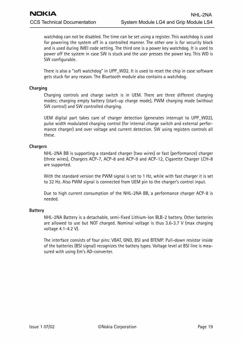
The Frequency synthesizerThe VCO frequency is locked using a PLL to a stable frequency source, which is a VCTCXO.The VCTCXO is running at 26 MHz. The Temperature effect is controlled with AFC. TheAFC is generated with a 11 bit conventional DAC in UEM.
The physical PLL is located inside the HAGAR RF-IC and is controlled via serial bus. ThePLL synthesizer consists of the following blocks :
• 64/65 CML prescaler• Programable R-, N- and A-dividers, • Phase detector and charge pump
64/65 NDIVADIV ϕ charge
pump
RDIV
SDATASCLK
SLE
1/4 1/2
2
OSC_IN
OUT_CP
2 2 2 2
1/2
1/4
22
4 4
44
TXI_0/TXI_180
DET
loopfilter VCO
AFC
INP_P_RX
INM_P_RX
Ante
nna
switc
h
RX
RX
TX
TXINP_G_RX
INM_G_RX
OUTP_P_TX
OUTP_G_TX
DCN2
DCN2
RX FilterCalibration
2
2 2
2 TXQ_0/TXQ_180
LNA_P
RXQ
RXI
OU
T_BB
1_I
OU
T_BB
1_Q
I_D
CN
2_I
I_D
CN
2_Q
C1_
BB1_
I
C2_
BB1_
I
C2_
BB1_
Q
C1_
BB1_
Q
Cp_
f_I
Cm
_f_I
Cp_
f_Q
Cm
_f_Q
Cp_
dtos
_I
Cm
_dto
s_I
Cp_
dtos
_Q
Cm
_dto
s_Q
Last edit 12:39 13.12.00Drawing85
Open collector
Open collector
0-40dB
BB_Gain
0-40dB
BB_Gain
DtoS
DtoS
BIQUAD
BIQUAD
E-GSM900
GSM1800
VRF_
RX
VBAT
TRF
VDIG
VPRE
VCP/GND_CP2
VLO
Reset
RF TEMPSENSOR
RFTEMPPWCDET
TXP
TXC
Vpctrl_fb
Vpct
rl_g
Vpct
rl_p
INP_LO/INM_LO
GNDRF_TX
VBB
VREF_RX
VB_E
XT
RB_
EXT
VB_DET
LNA_G
V_ANT_1/V_ANT_2
2
RFCLK
VR3
8 / 18 dB
8 / 18 dB
1/2 TOUT
0dB
SAW
SAW
Dir. Coupler
HAGAR
VR4
VR7
VREFRF02
VREFRF01
RXI_P
RXQ_P
VR5
AFC
RESET
RFBUSEN1RFBUSCLKRFBUSDA
TXCTXP
VBATTRF
TXQ_0/TXQ_180
TXI_0/TXI_180
2
2
HGR_TEMP
VR2
VR1
GND_BB / GNDRF_RX / GND_LO / GND_PRE /GND_CP / GND_DIG / GND_RX
VF_RX
LNAB_G
3dB
2
VTX_B_G
VTX_B_P
VtxB
_DC
S
VtxB
_GSM
OUTM_G_TX
OUTM_P_TX
SAW
LNA
LNA
LNAB_P
RFControls
RXQ_N
RXI_N
LPRFCLK26MHz
VR6
PA
VtxL
O_G
SM
VTXLO_G
CTRL
SAW
dB-2
dB-2
Page 34 Nokia Corporation Issue 1 07/02

CCS Technical Documentation System Module LG4 and Grip Module LS4NHL-2NA
Figure 20: Phase locked loop
The SHF local signal generated by a VCO module is fed into prescaler. The prescaler is adual-modulus divider. The output of the prescaler is fed to N- and A- divider which pro-duce the input to phase detector. The phase detector compares this signal to the refer-ence signal (400 kHz) which is obtained by dividing the VCTCXO output by reference R-divider. The output of the phase detector is connected to the charge pump which chargesor discharges integrator capacitor in the loop filter, depending on the phase of the mea-sured frequency compared to the reference frequency.
The loop filter, VCO and VCTCXO are all external synthesizer building blocks.
The loop filter performs filtering of the pulses and generates DC control voltage to theVCO. The loop filter also defines the step response of the PLL ( settling time ) and effectsthe stability of the loop. That’s why integrator capacitor has got a resistor for phasecompensation. The other filter components are for sideband rejection.
The dividers are controlled via serial bus: SDATA is for data, SCLK is serial clock for thebus and SLE is latch enable, which enables new data storage into dividers.
The transceiver LO signal is generated by VCO module. The VCO generates double fre-quency in GSM1800 and times four frequency in E-GSM900 compared to the actual RFchannel frequency. LO signal is divided by two or four in HAGAR ( depending on systemmode ).
This RF module comprises all RF functions of the engine. RF circuitry is located on oneside (B-side) of the PCB.
EMC leakage is prevented by using a metal B-shield, which screens the whole RF side(included FM radio) of the engine. The conductive (silicon or metal) gasket is usedbetween the PCB and the shield. The metal B-shield is separated to three blocks. The firstone include the FM radio. The second block include the PA, antenna switch, LNAs anddual RX SAW. The last block include the Hagar RF IC, VCO, VCTCXO, baluns and balancedfilters.
ADIV
NDIV÷64/65 ChargePumpϕ Loop
Filter VCO
RDIV( ÷65 )
CTRL
SDAT
A
SCLK
SLE
Res
et
÷2
÷4E-GSM900
GSM18003420 - 3840 MHz
AFC
26 MHz
HAGAR
Issue 1 07/02 Nokia Corporation Page 35
NHL-2NASystem Module LG4 and Grip Module LS4 CCS Technical Documentation
The baseband circuitry is located on the A-side of the board, which is shielded with ametallized frame and ground plane of the UI-board.
Maximum height inside on B-side is 1.8 mm. Heat generated by the circuitry is con-ducted out via the PCB ground planes and metallic B-shield
RF Frequency PlanFigure 21: RF Frequency plan
HAGAR
PLL
26 MHzVCTCXO
ff/2f/4
f
3420–3840MHz
925–960MHz
880–915MHz
I–signal
1805–1880MHz
ff/4
ff/2
Q–signal
I–signalI–signalI–signal RX
TXI–signal
Q–signal
1710–1785MHz
Page 36 Nokia Corporation Issue 1 07/02

CCS Technical Documentation System Module LG4 and Grip Module LS4NHL-2NA
DC characteristics
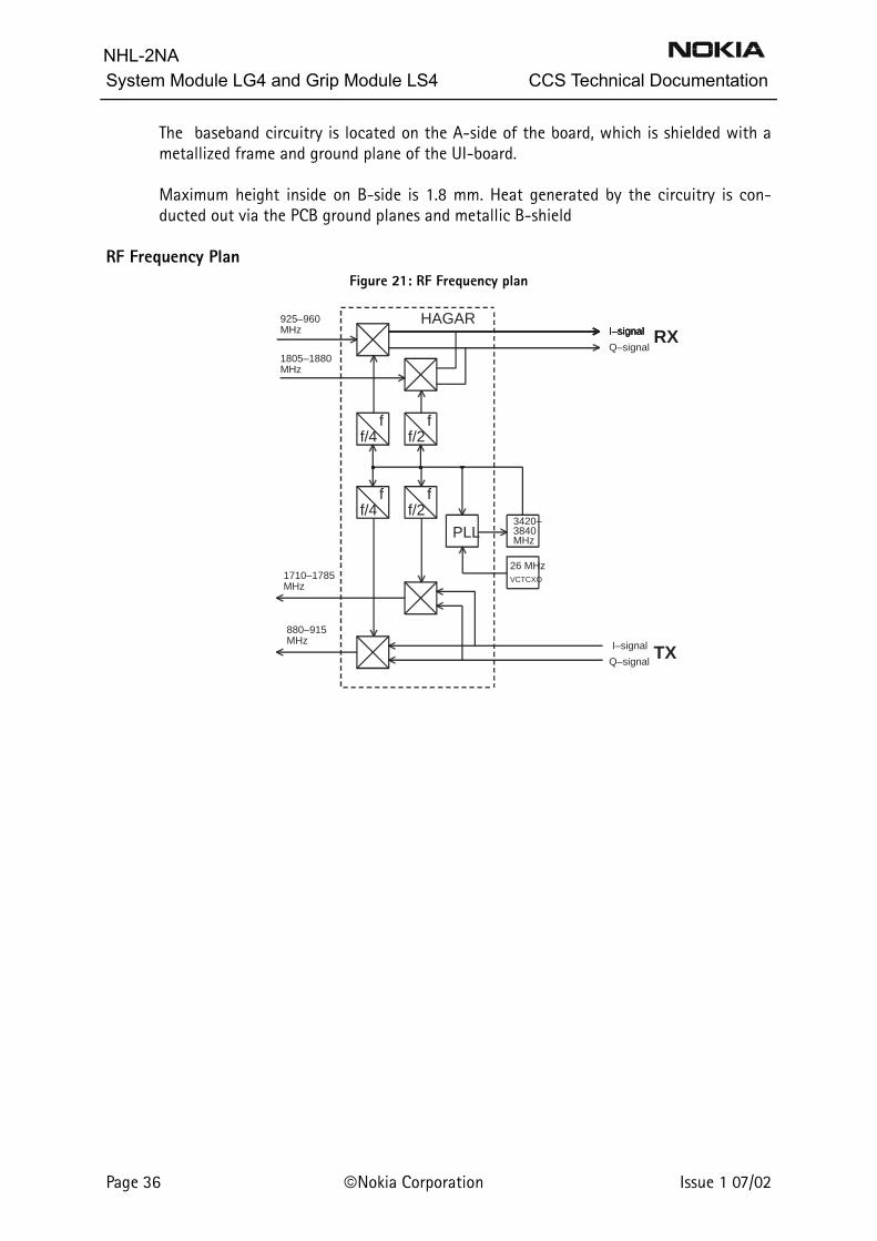
RegulatorsList of the needed supply voltages :
Volt. source LoadVR1a PLL charge pump (4,8 V)VR2 TX modulatorVR3 VCTCXO + bufferVR4 HAGAR IC (LNAs+mixer+DTOS)VR5 HAGAR IC (div+LO-buff+prescaler),VR6 HAGAR (Vdd_bb)VR7 VCOVrefRF01 ref. voltage for HAGARVrefRF02 ref. voltage for HAGARVbatt PA
Issue 1 07/02 Nokia Corporation Page 37
NHL-2NASystem Module LG4 and Grip Module LS4 CCS Technical Documentation
Power Distribution DiagramFigure 22: Power Distribution Diagram
BT102
VR1
VR5
VR4
VR3
VR2
VBATT
VREFRF02
VREFRF01
VR7
VR6
VFLASH01
UEM
PA
E-GSM900/GSM1800LNA
HAGAR
PLL charge pump
DTOS
PLL
Prescaler
LO buffers
Frequency dividers
RX Mixer
Reference voltage
RX reference voltage
BB section
TX IQ modulator
VCTCXO buffer
VCTXCO
VCO
PowerDetector
Page 38 Nokia Corporation Issue 1 07/02

CCS Technical Documentation System Module LG4 and Grip Module LS4NHL-2NA
RF characteristics
Transmitter characteristics
Receiver characteristics
Item Values (E-GSM / GSM1800)
Receive frequency range 925 ... 960 MHz / 1805...1880 MHz
Transmit frequency range 880 ... 915 MHz / 1710...1785 MHz
Duplex spacing 45 MHz / 95 MHz
Channel spacing 200 kHz
Number of RF channels 174 / 374
Power class 4 (2 W) / 1 (1 W)
Number of power levels 15 / 16
Item Values (E-GSM/GSM1800)
Type Direct conversion, nonlinear, FDMA/TDMA
LO frequency range 3520...3660 MHz / 3420...3570 MHz
Output power 2 W / 1 W peak
Gain control range min. 30 dB
Maximum phase error ( RMS/peak ) max 5 deg./20 deg. peak
Item Values, E-GSM/GSM1800
Type Direct conversion, Linear, FDMA/TDMA
LO frequencies 3700...3840 MHz / 3610...3760 MHz
Typical 3 dB bandwidth +/- 91 kHz
Sensitivity min. - 102 dBm (GSM1800 norm.cond. only)
Total typical receiver voltage gain ( from antenna to RX ADC )
86 dB
Receiver output level ( RF level -95 dBm ) 230 mVpp, single-ended I/Q signals to RX ADCs
Typical AGC dynamic range 83 dB
Accurate AGC control range 60 dB
Typical AGC step in LNA 30 dB GSM1800 25 dB EGSM
Usable input dynamic range -102 ... -10 dBm
RSSI dynamic range -110 ... -48 dBm
Compensated gain variation in receiving band +/- 1.0 dB
Issue 1 07/02 Nokia Corporation Page 39

NHL-2NASystem Module LG4 and Grip Module LS4 CCS Technical Documentation
RF Block DiagramFigure 23: RF Block Diagram
For further information see table on the next page.
UPPMCU, ASIC & DSP
UEMRFI and Codec
BB & RF regulatorsCharger switch
Codec samplesData to & from RF
Hagar
VCTCXOAFC
26 MHz
13 MHz
Tx I/QRx I/Q
RFtempTXC Vreg
Battery
PA LNA
Antenna Switch
VCO
4 GHz
Tx IQ modulator
LNA2, Mixer,AGC, DTOS
PLL, Dividers
RF control lines
RF_BB interface
RF_RF interface
Bluetooth
26 MHz
Page 40 Nokia Corporation Issue 1 07/02

CCS Technical Documentation System Module LG4 and Grip Module LS4NHL-2NA
Voltage Supplies and References
Signal name From To Parameter Min Typ Max Unit Function
VBAT Bat-tery
PA & UEM
Voltage 2.95 3.5 5.15 V Battery supply. Cut-off level of DCT4 regulators is 3.04V. Losses in PWB tracks and ferrites are taken account to mini-mum battery voltage level.
Current 2000
mA
Current drawn by PA when ”off”
0.8 2 mA
VR1 UEM VCP Voltage 4.6 4.75 4.9 V Supply for varactor for UHF VCO tuning.
Current 2 10 mA
Noise density 200 nVrms/ sqrt(Hz)
VR2 UEM VRF_TX Voltage 2.70 2.78 2.86 V Supply for part of trans-mit strip. Supply for TXI/Q-modulators.Current 65 100 mA
Noise densityf=100Hzf>300Hz
8055
nVrms/ sqrt(Hz)
VR3 UEM VCTCXO Voltage 2.70 2.78 2.86 V Supply for VCTCXO
Current 1 20 mA
Noise density 200 nVrms/ sqrt(Hz)
VR4 UEM VRF_RX Voltage 2.70 2.78 2.86 V Supply for Hagar RX; preamp., mixer,DTOSNoise density should have -20dB/° slope after 10kHz corner frequency
Current 50 mA
Noise densityf=100..10kHzf=100kHz
20020
nVrms/ sqrt(Hz)
VR5 UEM VDIG,VPRE,VLO
Voltage 2.70 2.78 2.86 V Supply for Hagar PLL; dividers, LO-buffers, prescaler,Current 50 mA
Noise densityBW=100Hz to 100kHZ
200 nVrms/ sqrt(Hz)
VR6 UEM VBB Voltage 2.70 2.78 2.86 V Supply for Hagar BB and LNA
Current 50 mA
Noise densityBW=100Hz to 100kHz
200 nVrms/ sqrt(Hz)
Issue 1 07/02 Nokia Corporation Page 41

NHL-2NASystem Module LG4 and Grip Module LS4 CCS Technical Documentation
VR7 UEM UHF VCO Voltage 2.70 2.78 2.86 V Supply for UHF VCO
Current 30 mA
Noise density100Hz<f<2kHz2kHz<f<10kHz10kHz<f<30kHz30kHz<f<90kHz90kHz<f<3MHz
7055353030
nVrms/ sqrt(Hz)
VrefRF01
UEM VREF_RX Voltage 1.334
1.35 1.366
V Voltage Reference for RF-IC.Note:Below 600Hz noise density is allowed to increase 20 dB/oct
Current 100 mA
Temp Coef -65 +65 uV/C
Noise densityBW=600Hz to 100kHz Note
55 nVrms/ sqrt(Hz)
VrefRF02
UEM VB_EXT Voltage 1.334
1.35 1.366
V Supply for RF-BB digital interface and some dig-ital parts of RF.
Current 100 mA
Temp Coef -65 +65 uV/C
Noise densityBW=100Hz to 100kHz
400 nVrms/ sqrt(Hz)
Page 42 Nokia Corporation Issue 1 07/02

CCS Technical Documentation System Module LG4 and Grip Module LS4NHL-2NA
ReceiverFigure 24: NHL-2NA Receiver chain
The receiver is a direct-conversion, dual-band linear receiver. RF signal energy gatheredby the antenna is fed via the antenna switch module to the 1st RX bandpass SAW filtersand MMIC LNAs. The RF antenna switch module provides for upper- and lower-bandoperation. The signal having been amplified by the LNA is then fed to 2nd RX bandpassSAW filters. Both of these 2nd RX bandpass SAW filters have UNBAL/BAL configuration toachieve the balanced feed for HAGAR. The discrete LNAs have three gain levels. The firstone is maximum gain, the second one is about -30dB ( GSM1800 ) and –25dB ( E-GSM900 ) below maximum gain and the last one is off state. The LNA gain selection iscontrolled directly by HAGAR.
The performance of the RX bandpass SAW filters are mainly responsible for defining thereceiver's blocking characteristics against spurious signals outside passband and the pro-tection against spurious responses.
The differential RX signal is amplified and mixed directly down to BB frequency inHAGAR. The LO signal is generated with external VCO. This VCO signal is divided by 2 (GSM1800 ) or by 4 ( E-GSM900 ). The PLL and dividers are internal to the HAGAR IC.From the mixer output to ADC input RX signal is divided into I- and Q-signals. Accuratephasing is generated in LO dividers. After the mixer DTOS amplifiers convert the differen-tial signals to single ended.
The DTOS has two gain stages. The first one has constant gain of 12dB and 85kHz cut offfrequency. The gain of second stage is controlled with control signal g10. If g10 is high(1) the gain is 6dB and if g10 is low (0) the gain of the stage is -4dB. The active channelfilters in HAGAR provide selectivity for channels (-3dB @ ± 91 kHz typ.). The integratedbaseband filter inside HAGAR is an active-RC-filter with two off-chip capacitors. LargeRC-time constants are needed in the channel select filter of the direct-conversionreceiver and are achieved with large off-chip capacitors because the impedance levelscould not be increased due to the noise specifications.
The baseband filter consists of two stages, DTOS and BIQUAD. DTOS is differential to sin-gle-ended converter having 8dB or 18dB gain. BIQUAD is modified Sallen-Key Biquad.Integrated resistors and capacitors are tunable. These are controlled with a digital con-
Issue 1 07/02 Nokia Corporation Page 43

NHL-2NASystem Module LG4 and Grip Module LS4 CCS Technical Documentation
trol word. The correct control words that compensate for the process variations of inte-grated resistors and capacitors and of tolerance of off chip capacitors are found with thecalibration circuit.
The next stage in the receiver chain is AGC-amplifier, also integrated into HAGAR. AGChas digital gain control via serial mode bms. AGC-stage provides gain control range (40dB, 10 dB steps) for the receiver and also the necessary DC compensation. Additional 10dB AGC step is implemented in DTOS stages.
DC compensation is made during DCN1 and DCN2 operations ( controlled via serial bus ).DCN1 is carried out by charging the large external capacitors in AGC stages to a voltagewhich effect a zero dc-offset. DCN2 set the signal offset to constant value ( VrefRF_021.35 V ). The VrefRF_02 signal is used as a zero level to RX ADCs.
Single ended filtered I/Q-signal is then fed to ADCs in BB. Input level for ADC is 1.45 Vppmax.
Rf-temp port is intended to be used for compensation of RX SAW filters thermal behav-ior. This phenomena will have impact to RSSI reporting accuracy. The current informa-tion is -35ppm/C for center frequency drift for all bands. This temperature informationis a voltage over two diodes and diodes are fed with constant current.
TransmitterTransmitter chain consists of two final frequency IQ-modulators for upper and lowerband, a dual power amplifier and a power control loop.
I- and Q-signals are generated by baseband. After post filtering (RC-network) they gointo IQ-modulator in HAGAR. There are separate outputs one for EGSM and one forGSM1800.
In EGSM branch there is a SAW filter before PA to attenuate unwanted signals andwideband noise from the Hagar IC.
The final amplification is realized with dual band power amplifier. It has two differentpower chains: one for EGSM and one for GSM1800. PA is able to produce over 2 W (0dBm input level) in EGSM band and over 1 W (0 dBm input level) in upperband band into50 ohm output . Gain control range is over 45 dB to get desired power levels and powerramping up and down.
Power control circuitry consists of discrete power detector (common for lower andupperband) and error amplifier in HAGAR. There is a directional coupler connectedbetween PA output and antenna switch. It is a dual band type and has input and outputsfor both systems. Directional coupler takes a sample from the forward going power withcertain ratio. This signal is rectified in a schottky-diode and it produces a DC-signal afterfiltering.
Page 44 Nokia Corporation Issue 1 07/02

CCS Technical Documentation System Module LG4 and Grip Module LS4NHL-2NA
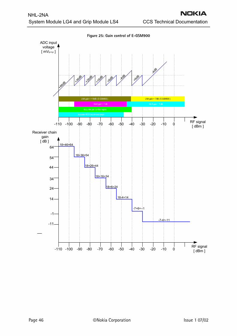
AGC strategyThe AGC-amplifier is used to maintain the output level of the receiver in within a certainrange. The AGC has to be set before each received burst with pre-monitoring or withoutpre-monitoring. In pre-monitoring, the receiver is switched on roughly 130µs before theburst begins, DSP measures received signal level and adjusts AGC-amplifiers via serialbus.
With this particular receiver architecture, there is 50 dB of accurate gain control in 10dB steps and large LNA step ( approximately 25dB for E-GSM900 and 30 for GSM1800).LNA AGC step size depends on channel to some extent.
In practice, this results in 6 accurate AGC steps and 2/3 non-accurate steps available tothe UPP depending on the band.
Because of the requirement from the GSM specifications that each MS should be able tomeasure and report it's RSSI accurately when receiving levels below –48dBm, and due tothe fact that the LNA step is not accurate, the LNAs should always be in the ON state inthis situation. For all signals in excess of –48dBm the MS will report a constant value.
Step no. AGC Step value AGC Gain Front-end LNA state
Front-endLNA gain
E-GSM900 GSM1800
1 0 -4 OFF -7 -11
2 1 +6 OFF -7 -11
3 2 +16 OFF -7 -11
4 3 -4 ON +18 +19
5 4 +6 ON +18 +19
6 5 +16 ON +18 +19
7 6 +26 ON +18 +19
8 7 +36 ON +18 +19
9 8 +46 ON +18 +19
Issue 1 07/02 Nokia Corporation Page 45
NHL-2NASystem Module LG4 and Grip Module LS4 CCS Technical Documentation
Figure 25: Gain control of E-GSM900
18+46=64
18+36=54
18+26=44
18+16=34
18+6=24
18-4=14
-7+6=--1
-7-4=-11
Receiver chain gain[ dB ]
64
54
44
34
24
14
-1
-11
RF signal[ dBm ]-110 -100 -90 -80 -70 -60 -50 -40 -30 -20 -10 0
-100 -90 -80 -70 -60 -50 -40 -30 -20 -10 0
LNA gain = +18dB ( E-GSM900 ) LNA gain = -7dB ( E-GSM900 )
DtoS gain = ? dB DtoS gain = ? dB
Accurate gain control region
ADC inputvoltage
[ mVp-t-p ]
RF signal[ dBm ]
+46d
B +36d
B
+26d
B
+16d
B
+6dB -4d
B+6
dB
-4dB
-110
Accurate RSSI requirment range
Page 46 Nokia Corporation Issue 1 07/02

CCS Technical Documentation System Module LG4 and Grip Module LS4NHL-2NA
Figure 26: Gain control of GSM1800
AFC functionThe AFC is used to lock the transceivers clock to frequency of the base station. The AFCvoltage is generated in baseband using an 11 bit DAC where an RC-filter is placed on theAFC control line to reduce the noise from the converter. The settling time requirement
-100 -90 -80 -70 -60 -50 -40 -30 -20 -10 0
LNA gain = +19dB ( GSM1800 ) LNA gain = -11dB ( GSM1800 )
DtoS gain = ? dB DtoS gain = ? dB
Accurate gain control region
ADC inputvoltage
[ mVp-t-p ]
RF signal[ dBm ]
+46d
B +36d
B
+26d
B
+16d
B
+6dB -4d
B +16d
B
+6dB
-4dB
-110
Accurate RSSI requirment range
19+46=65
19+36=55
19+26=45
19+16=35
19+6=25
19-4=15
-11+16=5
-11+6=--5
-11-4=-15
Receiver chain gain[ dB ]
65
55
45
35
25
15
5
-5
-15
RF signal[ dBm ]-110 -100 -90 -80 -70 -60 -50 -40 -30 -20 -10 0
Issue 1 07/02 Nokia Corporation Page 47

NHL-2NASystem Module LG4 and Grip Module LS4 CCS Technical Documentation
for the RC-network comes from signaling, i.e. how often PSW slots occur. They arerepeated after 10 frames. The AFC tracks the base station frequency continuously whichenables the transceiver to have a stable frequency reference.
The settling time requirement is also determined from the allowed start up-time. Whenthe transceiver is in sleep mode and ”wakes-up" to receive mode, there is only about 5ms for the AFC voltage to settle. When the first burst is received, the system clock has tobe settled into ± 0.1 PPM frequency accuracy. The VCTCXO module also requires 5 ms tosettle into the final frequency. The amplitude rises into full swing in 1 to 2 ms, but thefrequency settling time is higher so this oscillator must be powered up early enough.
DC-compensationDC compensation is made during DCN1 and DCN2 operations (controlled via serial bus).DCN1 is carried out by charging the large external capacitors in AGC stages to a voltagewhich cause a zero dc-offset. DCN2 set the signal offset to constant value (RXREF 1.35V). The RXREF signal is used as a zero level to RX ADCs.
Power control with analog temperature compensation schemeThe detected voltage level is compared by the HAGAR internal error-amplifier to the cur-rent TXC voltage level, which is generated by a DAC in BB. The TXC line is a so-called'raised cosine' shaped function, the effect of which is to minimize the switching tran-sients during the power ramp/decay phase. Because the dynamic range of the detector isnot wide enough to control the power ( more precisely, RF output voltage ) over thewhole range, there is an additional control line named TXP to work below detectable lev-els. The burst is enabled and set to rise with TXP until such time as the output level ishigh enough for feedback loop to kick-in.
The feedback loop controls the output level via a control pin in PA to the desired outputlevel and burst has got the waveform of TXC-ramps. Because feedback loops could beunstable, this loop is compensated with a dominating pole. This pole serves firstly todecrease gain of the error amplifier at higher frequencies which in turn increases thephase margin ( stability ). Secondly, it also provides for noise filtering on the TXC line.
Before power ramp the temperature information from detector is stored to Ctemp. Thistemperature information is used during the burst to compensate power levels at differ-ent temperatures. The TXP signal enables the antenna switch module to TX mode. Thereare two separate power control loops in HAGAR, one for E-GSM900 and the otherGSM1800.
Page 48 Nokia Corporation Issue 1 07/02

CCS Technical Documentation System Module LG4 and Grip Module LS4NHL-2NA
Figure 27: Power control feedback loop with analogue temperature compensation
-
+
-
+
HAGAR RFIC
POWER AMPLIFIER
EGSM900
GSM1800
R74647R C757
10n
R74533R C755
10n
R80122k
C8031p8
C8022n2C762
12p
V760Detector diode
L749Directional Coupler
AntennaSwitch
VpdGSM
VpdDCS
VANT_1 & VANT_2VtxBDCS
VtxBGSM
R8004k7
R80310k
R763100
C76112p
R73047R
C80482p
R80215k
VTX_B_GVTX_B_P
VB_DET
DET
VPCTRL_G
VPCTRL_P
VPCTRL_FB
R8044k7
GSM1800
E-GSM900
R7644k7
C76027p
TXP
TXC
C73127p
Issue 1 07/02 Nokia Corporation Page 49

NHL-2NASystem Module LG4 and Grip Module LS4 CCS Technical Documentation
Grip Module
Abbreviations
AEM Auxiliary Energy ManagementDC Direct CurrentGND GroundGPIO General Purpose Input OutputHW HardwareIF Inter FaceLED Light Emitting DiodeMCU Micro Controller UnitP(0) Column PortP(1) Row PortPWB Printed Wired BoardPWM Pulse Width ModulationSD_ Shut Down (active low)UEM Universal Energy ManagementUPP_WD2 Universal Phone Processor Wireless Data 2
IntroductionThe grip consists of Matrix keyboard, Vibra, Current gauge, Current pump, Keyboardbacklight LEDs, DC jack, Battery connector, Board to Board (BoBo) connector, Lockinglatch and magnet. There are five different versions of keymat; Latin, Stroke and BoPo-MoFo. The figure shows the construction of the grip.
The Grip PWB consists of four layers. Dimensions of the PWB are 60 mm x 46 mm x 0.6mm
Page 50 Nokia Corporation Issue 1 07/02

CCS Technical Documentation System Module LG4 and Grip Module LS4NHL-2NA
Figure 28: Construction of the Grip.
All test pads are shown in a figure below. The pin numbers of the connector X001 aredescribed in generally (1, 25, 26 and 50). Signals of the test pins can be seen on a nextpage.
Figure 29: Board to board connector and the test pads shown from the top side
Battery connector
DC jack
Grip PWB (Matrix Keyboard
& Backlight)
Current gauge & Current pump
Grip keymat cover
Grip cover
Vibra
Magnet
BoBo connector
Locking latch
Screws
Grip keymat
1
50 26
25
Issue 1 07/02 Nokia Corporation Page 51

NHL-2NASystem Module LG4 and Grip Module LS4 CCS Technical Documentation
Table 3: Signals and number of test pad
Figure 30: Bottom side of the grip PWB
Signal Test pad
Vbat J001
IPWM J008
ISD J007
VCHAR J019
BATGND J020
Col3 J005
Col2 J016
Row2 J015
Row3 J014
Row4 J013
Row5 J012
Called1 J021
Col4 J009
Btemp J003
Col5 J022
Vibra J017
BSI J002
BATGND
BTEMP
BSI
VBAT
CallLED1 PAD
VIBRA PADS
DC-JACK PADS
Page 52 Nokia Corporation Issue 1 07/02

CCS Technical Documentation System Module LG4 and Grip Module LS4NHL-2NA
General Interface between Grip and TransceiverNote: The table below is for your convenience.
Table 4: Signals between LG4 and LS4
PinLG4
PinLS4 Signal Name Connected
from-to
Signal Properties (Typ.)A/D - Levels –FRQ./Timing resolution
Description / Note
MJS pin number
1 25 BATGND LG4 LS4 Ana 0 DC Battery Ground
25
24 LG4 LS4 Ana 0 DC 24
2 23 LG4 LS4 Ana 0 DC 23
22 LG4 LS4 Ana 0 DC 22
3 21 VBAT LS4/LG4 LG4/LS4 Ana 0 - 4.2 V DC Battery Voltage
21
20 LG4 LG4/LS4 Ana 0 - 4.2 V DC 20
4 19 LG4 LG4/LS4 Ana 0 - 4.2 V DC 19
26 LG4 LG4/LS4 Ana 0 - 4.2 V DC 50
5 27 BSI LS4 LG4 Ana 0 - 2.7 V DC Battery Size indi-cator
49
6 28 BTEMP LS4 LG4 Ana 0 - 2.7 V DC Battery Tempera-ture
48
7 29 IPWM LS4 LG4 Ana 0 - 2.7 V DC Current gauge Data
47
8 30 ISD LG4 LS4 Ana 0 - 4.2 V DC Current Gauge On Off
46
9 31 BATGND (CPWM)
LG4 LS4 Ana 0 - 4.2 V DC Battery Ground (Charger Control PWM)
45
10 32 VCHAR LG4 LS4 Ana 0 - 4.2 V DC Charger Voltage
44
33 LG4 LS4 Ana 0 - 4.2 V DC 43
11 17 LG4 LS4 Ana 0 - 4.2 V DC 17
18 LG4 LS4 Ana 0 - 4.2 V DC 18
12 34 CGND LG4LG4LG4LG4
LS4 Ana 0 DC Charger Ground
42
35 LS4 Ana 0 DC 41
13 15 LS4 Ana 0 DC 15
16 LS4 Ana 0 DC 16
Issue 1 07/02 Nokia Corporation Page 53

NHL-2NASystem Module LG4 and Grip Module LS4 CCS Technical Documentation
14 14 VIBRA LG4 LS4 Ana 0 - 4.2 V DC Vibra Con-trol
14
36 LG4 LS4 Ana 0 - 4.2 V DC 40
15 37 COL5 LS4 LG4 Dig 0 - 1.8 V DC Keyboard Column signal
39
16 38 Called1 LG4 LS4 Ana 0 - 4.2 V DC Keyboard lights Con-trol
38
13 13
17 39 Col2 LS4 LG4 Dig 0 - 1.8 V DC Keyboard Column Signal
37
18 40 Col3 LS4 LG4 Dig 0 - 1.8 V DC Keyboard Column Signal
36
12 12
19 41 VBAT LS4/LG4 LG4/LS4 Ana 0 - 4.2 V DC Battery Voltage
35
42 LG4 LG4/LS4 Ana 0 - 4.2 V DC 34
20 10 LG4 LG4/LS4 Ana 0 - 4.2 V DC 10
11 LG4 LG4/LS4 Ana 0 - 4.2 V DC 11
21 43 BATGND LG4 LS4 Ana 0 DC Battery Ground
33
44 LG4 LS4 Ana 0 DC 32
22 8 LG4 LS4 Ana 0 DC 8
9 LG4 LS4 Ana 0 DC 9
23 45 Row2 LG4 LS4 Dig 0 - 1.8 V DC Keyboard Row Signal
31
24 46 Row3 LG4 LS4 Dig 0 - 1.8 V DC Keyboard Row Signal
30
25 47 Row4 LS4 LG4 Dig 0 - 1.8 V DC Keyboard Row Signal
29
26 48 Row5 LS4 LG4 Dig 0 - 1.8 V DC Keyboard Row Signal
28
27 49 Col4 LS4 LG4 Dig 0 - 1.8 V DC Keyboard Column Signal
27
28 5 VBAT LS4/LG4 LG4/LS4 Ana 0 - 4.2 V DC Battery Voltage
5
6 LG4 LG4/LS4 Ana 0 - 4.2 V DC 6
29 7 LG4 LG4/LS4 Ana 0 - 4.2 V DC 7
50 LG4 LG4/LS4 Ana 0 - 4.2 V DC 26
30 1 BATGND LG4 LS4 Ana 0 DC Battery Ground
1
2 LG4 LS4 Ana 0 DC 2
31 3 LG4 LS4 Ana 0 DC 3
4 LG4 LS4 Ana 0 DC 4
Page 54 Nokia Corporation Issue 1 07/02

CCS Technical Documentation System Module LG4 and Grip Module LS4NHL-2NA
Figure 31: As seen from the soldering pad side
Figure 32: General view of the connectors and a physical structure
50 1
1
31
Grip module, LS4 (from the top side)
Transceiver Unit, LG4 (from the top side)
Hot Bar soldering BoBo Connector
Flex Connector
1 50
Issue 1 07/02 Nokia Corporation Page 55
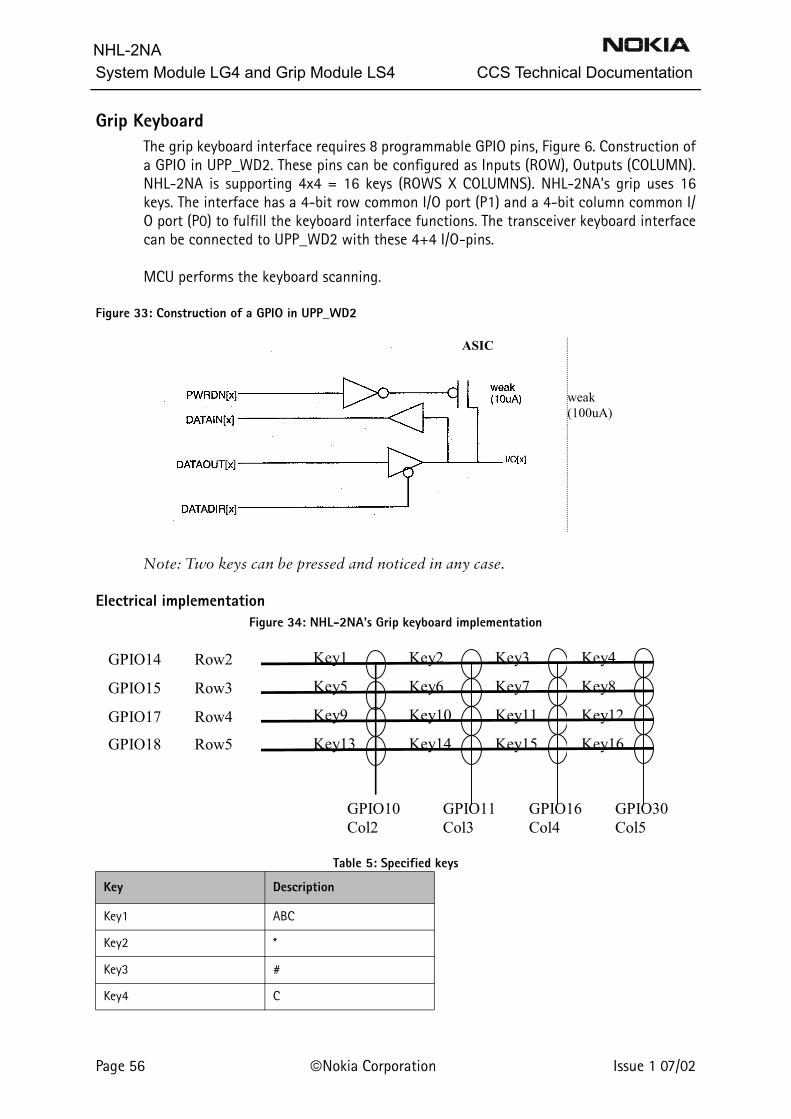
NHL-2NASystem Module LG4 and Grip Module LS4 CCS Technical Documentation
Grip KeyboardThe grip keyboard interface requires 8 programmable GPIO pins, Figure 6. Construction ofa GPIO in UPP_WD2. These pins can be configured as Inputs (ROW), Outputs (COLUMN).NHL-2NA is supporting 4x4 = 16 keys (ROWS X COLUMNS). NHL-2NA's grip uses 16keys. The interface has a 4-bit row common I/O port (P1) and a 4-bit column common I/O port (P0) to fulfill the keyboard interface functions. The transceiver keyboard interfacecan be connected to UPP_WD2 with these 4+4 I/O-pins.
MCU performs the keyboard scanning.
Figure 33: Construction of a GPIO in UPP_WD2
Note: Two keys can be pressed and noticed in any case.
Electrical implementationFigure 34: NHL-2NA's Grip keyboard implementation
Table 5: Specified keys
Key Description
Key1 ABC
Key2 *
Key3 #
Key4 C
weak (100uA)
ASIC
Key13
Key9 Key10
Key6 Key5
Key1 Key2 Key3
Key7
Key11
Key14 Key15
Key4
Key8
Key12
Key16
GPIO14 Row2
GPIO15 Row3
GPIO17 Row4
GPIO10Col2
GPIO11Col3
GPIO18 Row5
GPIO16 Col4
GPIO30 Col5
Page 56 Nokia Corporation Issue 1 07/02

CCS Technical Documentation System Module LG4 and Grip Module LS4NHL-2NA
Unit limitsTable 6: Unit limits
VibraThe NHL-2NA grip module includes a vibra. The Nokia code is available in the spare partlist.
Electrical interfaceVibra needs one line from flex for operating. The line is VIBRA.
The VIBRA line is also connected to BATGND via 33nF and 2.2uF capacitors for filteringthe interference. Capacitors locate near to the vibra. Vibra driver has also protectivediodes (see Electrical interface of Vibra) because of inductive characteristic of the vibra.
The vibra component is controlled by UEM vibra driver.
Key5 1
Key6 2
Key7 3
Key8 0
Key9 4
Key10 5
Key11 6
Key12 Send
Key13 7
Key14 8
Key15 9
Key16 End
Unit Min. Nom. Max.
Pull up voltage, in UPP_WD2(Measured from RowXX in)
1.65 V 1.8 V 1.95 V
Issue 1 07/02 Nokia Corporation Page 57

NHL-2NASystem Module LG4 and Grip Module LS4 CCS Technical Documentation
Figure 35: Electrical interface of Vibra
Table 7: Electrical properties of the VIBRA signal
Figure 36: Principle figure of the VIBRA signal
Unit Min Nom Max
Current via vibra 50 mA 80 mA 135 mA
Vbat 3.0 V 3.7 V 4.2 V
Possible VIBRA signal frequency64Hz, 129Hz, 258Hz and 520Hz
VIBRA pulse duty cycle 3% 47% 97%
BoBo CONNECTOR
Vbat
M
Vbat
Principle figure of the driver in UEM
PWM 33nF 2.2uF
VIBRA line
LG4 board LS4 board
Vbat
0 V
positive cycle
negativecycle
Page 58 Nokia Corporation Issue 1 07/02

CCS Technical Documentation System Module LG4 and Grip Module LS4NHL-2NA
Current GaugeThe current gauge is placed to the positive battery line terminal so that all current flowin either direction is registered. See Electrical-implementation of the current gauge.
The LM3822 component is well suited for the purpose since its serial resistance is only 3mW and it has a PWM output. The current value and direction are indicated by the dutycycle of the PWM signal. Shutdown is controlled with a specific pin.
Table 8: Properties of the current gauge
Note: External components (2x100nF capacitors) are needed.
Interfacing the current gaugeAEM (locates on LG4) receives the PWM signal and calculates average duty cycle valuesto a register. SW can define how many PWM cycles are averaged, whether or not to givean interrupt to UPP_WD2 after averaging is done. The PWM value for the last PWM cyclecan also be found out. The shutdown control is also through AEM. AEM gives an inter-rupt to UPP_WD2 indicating that current measurement is ready.
Note: Shutdown control is used to disable and enable the gauge.
Table 9: Signal properties
Unit Min Nom Max
Resistance(between pins 1 and 8)
3 mΩ
Current Range(average)
- 1.0 A +1.0 A
Supply Voltage 2.5 V 5.5 V(Absolute Max)
Current consumption 2.5 uA (shut down) 90 uA (active)
Cycle length(average)
52 ms
Package MSOP-8
BATGND 0 V
Peak Current (200ms) 10A(Absolute Max)
Signal Level Polarity I / O to / from Pin
Sense + / Vdd Vbat 1
BATGND Ground 2
Filter + ext. capacitor 3
Filter - ext. capacitor 4
ISD Vbat active Low Input AEM 5
Issue 1 07/02 Nokia Corporation Page 59

NHL-2NASystem Module LG4 and Grip Module LS4 CCS Technical Documentation
Figure 37: Electrical-implementation of the current gauge
Note: BATGND is the ground of the grip, not charger ground
TEST Ground 6
IPWM Vbat active HIGH Output AEM 7
Sense - Transceiver Vbat 8
Battery 8 7 6 5
1 2 3 4
Battery Con
NATIONAL's Current meter
component LM3822
BoBo Con
Vbat
IPWM
ISD
100n
100n
BATGND
Page 60 Nokia Corporation Issue 1 07/02

CCS Technical Documentation System Module LG4 and Grip Module LS4NHL-2NA
BacklightNHL-2NA grip keyboard uses six white backlight LEDs. These LEDs are “smart LEDs”(0.6mm height). The LED type is LWL88S, NMP code 4860331. NHL-2NA grip uses bright-ness groups M1-M2, N1-N2 and P1. There is only one brightness group in one grip-mod-ule.
Electrical interfaceThe idea is to connect these six LEDs parallel. LEDs are using current that is taken frombattery voltage. The voltage is controlled by charge pump (NMP code 4341137) and thecurrent by serial resistor. The idea of the charge pump is to keep the supply voltage of theLEDs constant although Vbat changes. Serial resistors limit the current that goes to LEDs.Current for one LED is ~4mA. The circuit and LEDs consume ~52mA current.
LEDs need one line of flex (Called1). Called1 controls the charge pump SD pin. Called1signal rises close to Vbat voltage (required for the SD signal in specification of the cur-rent pump). The output of the current pump is 4.1V (@Vbat 3.0V to 4.2V).
Figure 38: Electrical implementation of the grip keyboard backlight
Called1 10u SD
330n 330n
4u7
1u
1k
37R4 // 49R9 1%
6 x LED
Vbat Vbat
100k
BatGND
BatGND
BatGND
BatGND
Vout Vin
C1- C1+
C2- C2+
CFilt
B o B o C O N
Issue 1 07/02 Nokia Corporation Page 61

NHL-2NASystem Module LG4 and Grip Module LS4 CCS Technical Documentation
Hall Sensor and MagnetNHL-2NA uses the Infineon Hall sensor TLE 4917 (NMP code 4341087) and magnet tofind out the open/close position of the grip. The hall sensor component is in the trans-ceiver unit and the magnet is in the grip module. See figure 9 for more information.
MagnetNHL-2NA magnet (NMP code 6490201) locates on grip module.
Figure 39: Basic principle of the hall-sensor implementation
Note: Hall sensor is independent on magnet flow direction, i.e. the magnet can beassembled in two ways; North-pole up or down.
Hall-Sensor
N
S GRIP LS4
Transceiver LG4
Page 62 Nokia Corporation Issue 1 07/02

CCS Technical Documentation System Module LG4 and Grip Module LS4NHL-2NA
DC Jack and Battery ConnectorGrip has battery connector (NMP code 5400255), DC-jack (NMP code 5400251) andboard to board connector (NMP code 5460059). Signals of the battery connector and DCjack are described in table below. See also Signals between LG4 and LS4. NHL-2NA usesBLB-2 battery.
NOTE: Table below is for your convenience.
Table 10: Battery connector signals.
Table 11: DC jack signals
Electrical interfaceThe basic principle of connections between connectors are described below.
Figure 40: Figure 15. Electrical implementation of the connectors
Connector Signal To From Value (BLB-2)
BatteryVbat (sense) Current Gauge Battery con. 3.2 V - 4.2 V
Btemp BoBo Battery con. 1979kΩ - 4.26 kΩ (- 40°C - + 90°C)
BSI BoBo Battery con. 68kΩ
BATGND BoBo Battery con. 0 V
Connector Signal To From Value (accepted charger)
DC jackCGND BoBo DC jack. 0 V
VCHAR BoBo DC jack. 5.0 V – 9.8 V
CGND BoBo DC jack. 0 V
Sense +/-Vdd
(Btemp) (BSI)
(CGND) (VCHAR)
(ISD) (IPWM) (Vbat)
(BATGND)
BoBo
CONNECTOR
Current Gauge
Battery Connector
DC jack
Issue 1 07/02 Nokia Corporation Page 63

NHL-2NASystem Module LG4 and Grip Module LS4 CCS Technical Documentation
This page intentionally left blank.
Page 64 Nokia Corporation Issue 1 07/02