Embed Size (px)
Citation preview

Copyright © Cirrus Logi(All Rights Reserhttp://www.cirrus.com
AIN1+
AIN1-
CRYSTAL4.9152 MHz
CS5530
A1A0
SCLKSDOSDICS
Interface Header
AIN1+
AIN1-
VREF-
VREF+VREF Source Select
VREF+
VREF-
VA-
CDB5530U
CDB5530U Evaluation Board and Software
FeaturesUSB Communication with PC
On-board Microcontroller
On-board Voltage Reference
Evaluation Software– Register Setup & Chip Control
– FFT Analysis
– Time Domain Analysis
– Noise Histogram Analysis
Interface Header for External Microcontroller
General DescriptionThe CDB5530U is an inexpensive tool designed to eval-uate the functionality and performance of the CS5530.The CS5530 data sheet should be read and consultedwhen using the CDB5530U evaluation board.
The evaluation board includes a C8051F320 microcon-troller with a USB interface. The microcontroller controlsthe serial communication between the evaluation boardand the PC via the firmware, enabling quick and easy ac-cess to all of the CS5530’s registers and functions.
The CDB5530U includes software for Data Capture,Time Domain Analysis, Histogram Analysis, and Fre-quency Domain Analysis.
ORDERING INFORMATIONCDB5530U Evaluation Board
c, Inc. 2006ved)
C8051F320Microcontroller
RESETCIRCUITRY
LT1019
VD+VA+ GND +5 V
USBCONNECTOR
NOV ‘06DS742DB1

CDB5530U
TABLE OF CONTENTS1. HARDWARE ............................................................................................................................. 3
1.1 Introduction ........................................................................................................................ 31.2 Evaluation Board Overview ................................................................................................ 3
1.2.1 Analog Section ...................................................................................................... 31.2.2 Digital Section ....................................................................................................... 41.2.3 Power Supply Section ........................................................................................... 4
2. SOFTWARE .............................................................................................................................. 82.1 Installation Procedure ........................................................................................................ 82.2 Using the Software ............................................................................................................. 8
2.2.1 Start-Up Window ................................................................................................... 82.2.2 Setup Window ....................................................................................................... 92.2.3 Data Collection Window ...................................................................................... 122.2.4 Configuration Window ......................................................................................... 13
2.3 Collecting Data Sets ........................................................................................................ 142.4 Saving and Printing Data ................................................................................................. 142.5 Retrieving Saved Data From a File .................................................................................. 142.6 Analyzing Data ................................................................................................................. 142.7 Histogram Information ...................................................................................................... 152.8 Frequency Domain Information ........................................................................................ 152.9 Time Domain Information ................................................................................................. 15
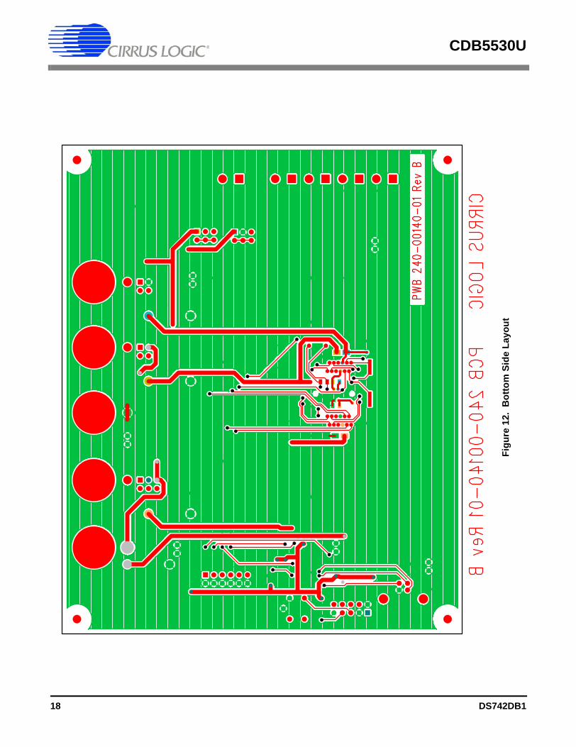
3. BOARD LAYOUT ................................................................................................................... 16
LIST OF FIGURESFigure 1. Analog Section ................................................................................................................. 5Figure 2. Digital Section .................................................................................................................. 6Figure 3. Power Supply ................................................................................................................... 7Figure 4. Evaluation Software Start-Up Screen .............................................................................. 8Figure 5. CDB5530U Setup Window............................................................................................... 9Figure 6. CDB5530U Calibration Window ..................................................................................... 10Figure 7. CDB5530U Data Collection Window.............................................................................. 12Figure 8. CDB5530U Configuration Window................................................................................. 13Figure 10. Top Silkscreen ............................................................................................................. 16Figure 11. Top Side Layout ........................................................................................................... 17Figure 12. Bottom Silkscreen ........................................................................................................ 18Figure 13. Bottom Side Layout...................................................................................................... 19
LIST OF TABLESTable 1. Voltage Reference Selection for VREF+ .......................................................................... 4Table 2. Voltage Reference Selection for VREF- ........................................................................... 4
2 DS742DB1

CDB5530U
1. HARDWARE1.1 IntroductionThe CDB5530U evaluation board provides a quick means of evaluating the CS5530 Analog-to-DigitalConverter (ADC). The CS5530 is a highly integrated ∆Σ ADC which uses charge-balance techniques toachieve 24-bit performance. The CS5530 includes a very low noise chopper-stabilized instrumentationamplifier (12 nV/sqrt(Hz) @ 0.1 Hz) with a fixed gain of 64×. This ADC also includes a fourth-order ∆Σmodulator followed by a digital filter which provides twenty selectable output word rates of 6.25 Hz,7.5 Hz, 12.5 Hz, 15 Hz, 25 Hz, 30 Hz, 50 Hz, 60 Hz, 100 Hz, 120 Hz, 200 Hz, 240 Hz, 400 Hz, 480 Hz,800 Hz, 960 Hz, 1.6 kHz, 1.92 kHz, 3.2 kHz and 3.84 kHz (XIN = 4.9152 MHz).
1.2 Evaluation Board OverviewThe CDB5530U evaluation board is partitioned into two main sections — analog and digital. The analogsection consists of the CS5530 and a precision voltage reference. The digital section consists of the mi-crocontroller, the reset circuitry, and the USB interface. The board also has power supply connectionswhich accommodate all of the various supply options of the CS5530.
The evaluation board’s analog section operates from either a single +5 V, dual ±2.5 V, or dual ±3 V powersupply. The evaluation board interfaces the CS5530 to an IBM® compatible PC with a USB interface. Toaccomplish this, the board comes equipped with a microcontroller and a USB cable which physically in-terfaces the evaluation board to the PC. The software provides easy access to the internal registers of theCS5530, and provides a means to display and evaluate the performance of the ADC in the time domainor the frequency domain.
1.2.1 Analog SectionThe CS5530 is a high-precision ∆Σ converter designed to accurately measure one fully differential analogvoltage input while operating from a 4.9152 MHz crystal.
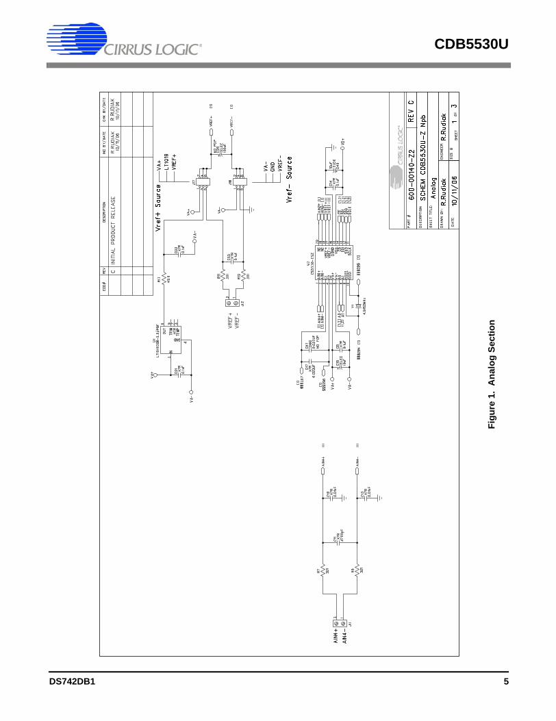
The evaluation board provides screw terminals labeled AIN1+ & AIN1- to connect input signals to the sin-gle input channel. The sensor’s output is filtered by a simple RC network at the channel input to reduceany interference picked up by the input leads. The 3 dB corner of the filter is approximately 52 kHz, differ-ential and 56 kHz, common mode. Figure 1 illustrates the schematic of the analog section.
The evaluation board provides three voltage reference options for VREF+ and VREF-. The three refer-ence options for VREF+ include: VA+, the on-board LT1019 voltage reference, and external input (J12).Table 1 illustrates the options available. With the J17 jumper in the VA+ position, the reference is suppliedby the VA+ analog supply. With the J17 jumper in the LT1019 position, the LT1019 provides a +2.5 V ref-erence (the LT1019 was chosen for its low drift, typically 5ppm/°C). By setting the J17 jumper to theVREF+ position, the user can supply an external voltage reference to J12’s VREF+ input.
The three reference options for VREF- include: VA-, GND, and external input (J12). Table 2 illustrates theoptions available. With the J18 jumper in the VA- position, the reference is supplied by the VA- analogsupply. With the J18 jumper in the GND position, the VREF- pin is connected to the board ground. Bysetting the J18 jumper to the VREF- position, the user can supply an external voltage reference to J12’sVREF- input.
DS742DB1 3

CDB5530U
Table 1. Voltage Reference Selection for VREF+ Table 2. Voltage Reference Selection for VREF-
1.2.2 Digital SectionFigure 2 illustrates the schematic of the digital section. It contains the microcontroller, USB interface, EE-PROM, JTAG header, reset circuitry, and an external interface header. The microcontroller interfaces theSPI™ and MICROWIRE™ compatible serial port of the CS5530 with the USB connection to the PC. Notethat the SCLK and SDI signals are level shifted to support both +3.3 V and +5 V digital operation.
The microcontroller EEPROM is used to store firmware. An external interface header, J19, is provided toallow the CDB5530U to be interfaced with an external microcontroller. To use this serial interface, the0 ohm resistors R9, R10, R23, and R27 should be removed to disconnect the on-board microcontrollerfrom the serial interface.
1.2.3 Power Supply SectionFigure 3 illustrates the power supply connections to the evaluation board. VA+ supplies the positive ana-log supply for the CS5530 and the LT1019 reference. Header J14 allows the VA+ supply to be sourcedfrom either the VA+ binding post (J2), or from the +5 V binding post (J3). VA- supplies the negative analogsupply for the analog section. Header J13 allows the VA- supply to be sourced from either the VA- bindingpost (J1), or connected to the board ground. Note that the VA- supply should be connected to groundwhen powering the CDB5530U from a single +5 V analog supply. VD+ supplies the digital section of theADC and level shifters. Header J15 allows the VD+ supply to be sourced from the VD+ binding post (J5),the +5 V binding post (J3), or the regulated +3.3 V supply derived from the microcontroller. The +5 V bind-ing post supplies the microcontroller’s internal regulator.
Reference Description J17
VA+Selects Positive Analog Power
Supply
LT1019Selects on-Board LT1019 Reference
(5ppm/°C)
VREF+Selects External
Reference Source (J12)
O O VREF+O O VREF+O O VREF+
VA+ LT1019 REF+
O O VREF+O O VREF+O O VREF+
VA+ LT1019 REF+
O O VREF+O O VREF+O O VREF+
VA+ LT1019 REF+
Reference Description J18
VA-Selects Negative
Analog Power Supply
GND Selects Board Gnd
VREF-Selects External
Reference Source (J12)
O O VREF-O O VREF-O O VREF-
VA- GND REF-
O O VREF-O O VREF-O O VREF-
VA- GND REF-
O O VREF-O O VREF-O O VREF-
VA- GND REF-
4 DS742DB1
CDB5530U
2. SOFTWAREThe evaluation board comes with software and a USB cable to link the evaluation board to the PC. Thesoftware is designed to run under Windows® 2000 or later.Important: DO NOT connect the evaluation board to the PC until you have completed the installation procedure andhave installed the USB drivers as described below.
2.1 Installation Procedure2.1.1 CDB5530U GUI Software Installation Instructions
1. Ensure the CDB5530U USB cable is disconnected from the PC.
2. Open GUI software installation folder CDB553x_cvidistkit.Eval5534U Volume1.
3. Run SETUP.EXE by double clicking on the filename.
4. Select Next, I Accept License Agreement, Next, Next, Finish.
2.1.2 Installing the USB Drivers1. Apply power to the CDB5530U. Press and release the Reset switch, S1.
2. Use the included USB cable to connect the CDB5530U to the PC. The PC operating system shouldautomatically launch the Found New Hardware wizard.
3. From the installation wizard, select Install from a list or specific location (Advanced). Select Searchfor the best driver in these locations.
4. Select Include this location in the search.
5. Click the Browse... button.
6. Go to folder C:/Program Files/Eval5534U/Driver and click OK.
7. Press the Next button.
8. A Hardware Installation dialog will appear. Press Continue Anyway.
9. Select Browse... and go to folder C:/Program Files/Eval5534U/Driver. Press Open.
10. A Files Needed dialog will appear. Press OK.
11. The Found New Hardware wizard will appear. Press the Finish button.
2.1.3 Running the GUIRun the program by selecting Start All Programs Eval5534U Eval5534_U.
2.2 Using the SoftwareBefore launching the evaluation program, the user should select the proper jumper settings as describedin Section 1.
8 DS742DB1
CDB5530U
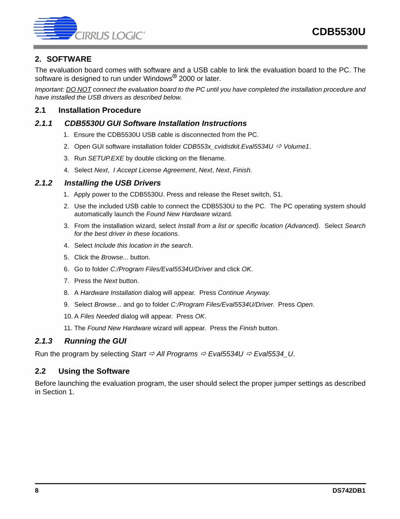
2.2.1 Start-Up WindowWhen the evaluation program is launched, the Start-Up window will appear. This window contains infor-mation concerning the software’s title, revision number, copyright date, etc.
Figure 4. Evaluation Software Start-Up Screen
At the top of the screen is a menu bar which displays user options. The menu bar item Window is initiallydisabled to prevent conflicts with other serial communications devices. After selecting the data source inthe Options menu, the Window menu item will become available.
2.2.1.1 Options
The Options menu item allows the user to select the source of the data and to configure the appearanceof the graphs. The user has two options for the data source: USB and File. If the USB setup is selected,the evaluation software will be ready to communicate with the CDB5530U via the USB connection. At thispoint, the Part menu item is active and the appropriate CS5530U device can be selected. If the File sourceis selected, the evaluation software will prompt the user to select the appropriate data file. This option al-lows the user to view previously captured data without having a CDB5530U connected to the PC. SeeSection 2.5, "Retrieving Saved Data From a File" on page 14 for more details.
The Plot Options window can be accessed by pulling down the Options menu and clicking on Plot Options.In this window, the user can change the background color, the plot line color, and the peak indicator color.The harmonic and peak indicators can also be turned on or off in this window.
DS742DB1 9

CDB5530U
2.2.1.2 Window
After the user selects the appropriate setup, the Window option becomes available in the Start-Up win-dow. The Window pull-down has three options: Start-Up Window, Setup Window, and Data CollectionWindow.
2.2.2 Setup WindowThe Setup window allows the user to access the internal registers of the CS5530. See Figure 5.
Figure 5. CDB5530U Setup Window
In the Setup window, all of the ADC’s registers are displayed as hexadecimal values. The Configurationregister’s settings are also defined in this window.
Update Registers: The Update Registers button will read all the register values from the CS5530 andupdate the hexadecimal values displayed on the screen. It is a good idea to press the Update Registersbutton when entering the Setup window, or after modifying any registers to reflect the current status of thepart.
Reset Serial Port: When this button is pressed, the software will send the synchronization sequence (dis-cussed in the CS5530 data sheet) to the ADC. This sequence brings the CS5530’s serial port back to thecommand mode, but does not reset any of the registers in the part.
Reset Part: When this button is selected, a ‘1’ is written to the RS bit in the Configuration register to resetthe part. After a reset, the registers will all return to their default values as discussed in the CS5530 datasheet.
Read Data: This button will instruct the ADC to begin performing repeated single (fully-settled) conver-sions on the setup channel specified by the Setup Register box. The results of the most recent conversion
10 DS742DB1

CDB5530U
are displayed in the Conversion Data box, as well as the Channel (always “1” for CS5530) and Overflowindicator bits for each conversion. The software will halt the data collection process when the user pressesthe Stop button.
Configuration Register: In the Configuration Register box, the contents of the Configuration register aredisplayed, and can be modified by typing a hexadecimal value in the Hexadecimal: box, or by changingany of the values below the Hexadecimal: box to the desired settings.
Note: When changing the value of the reset system bit to “1” (RS, bit 29 in the Configuration register), the part willbe reset, and all registers will return to their default values. It is a good idea to select the Update Registers buttonafter performing a reset to update the screen with the new register values.
Offset / Gain Registers: In the Offset Registers / Gain Registers box, the contents of the offset and gainregisters are displayed in hexadecimal. These registers can all be modified in the Calibration window,which is accessed when the user selects the Calibration Window button.
Calibration Window: The Calibration window (Figure 6) permits the user to access the calibration regis-ters of the CS5530 and also perform system offset or gain calibrations. Prior to performing calibrationshowever, the Configuration register should be modified to configure the part for the desired operatingmode (see Section 2.2.4, "Configuration Window" on page 13 for more details). Note that offset calibrationshould be performed before gain calibration to ensure accurate results. Refer to the CS5530 data sheetfor more details.
Figure 6. CDB5530U Calibration Window
System Offset Calibrations:
1) Attach an input signal to the AIN± inputs that you want to calibrate as zero. Note that the groundedinput must be within the common mode range of the amplifier for proper operation.
2) Activate the system offset calibration by pressing the System OFFSET button.3) When the calibration is complete, the screen will automatically update the offset register with the
new value.
System Gain Calibrations:
1) Attach a full-scale input to the AIN± inputs of the CDB5530U.2) Activate the system gain calibration by pressing the System GAIN button.3) When the calibration is complete, the screen will automatically update the gain register with the
new values.
DS742DB1 11

CDB5530U
2.2.3 Data Collection WindowThe Data Collection window (Figure 7) allows the user to collect sample sets of data from the CS5530 andanalyze them using time domain, FFT, and histogram plots. The Data Collection window is accessiblethrough the Window option, or by pressing <F3>.
Figure 7. CDB5530U Data Collection Window
Time Domain / FFT / Histogram Selector: This menu selects the type of data processing to perform onthe collected data and display in the plot area. Refer to Section 2.6, "Analyzing Data" on page 14 for moreinformation.
Collect Button: This button will collect data from the part, to be analyzed in the plot area. See Section2.3, "Collecting Data Sets" on page 14 for more information.
Config Button: This button will bring up the Configuration window, in which the user can modify the datacollection specifications. See Section 2.2.4, "Configuration Window" on page 13.
Output Button: This button will bring up a window in which the user can output the data to a data file forlater use, print out a plot, or print out the entire screen.
Zoom Button: This button allows the user to zoom in on the plot by selecting two points in the plot area.Press the Restore button to return to the normal data plot, or press the Zoom button again to zoom in evenfurther.
Setup Select Box: This box does not apply to the CS5530 as this device doe not contain a Setup register.
12 DS742DB1
CDB5530U
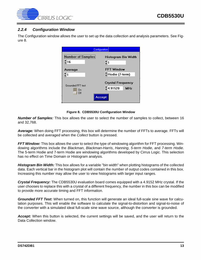
2.2.4 Configuration WindowThe Configuration window allows the user to set up the data collection and analysis parameters. See Fig-ure 8.
Figure 8. CDB5530U Configuration Window
Number of Samples: This box allows the user to select the number of samples to collect, between 16and 32,768.
Average: When doing FFT processing, this box will determine the number of FFTs to average. FFTs willbe collected and averaged when the Collect button is pressed.
FFT Window: This box allows the user to select the type of windowing algorithm for FFT processing. Win-dowing algorithms include the Blackman, Blackman-Harris, Hanning, 5-term Hodie, and 7-term Hodie.The 5-term Hodie and 7-term Hodie are windowing algorithms developed by Cirrus Logic. This selectionhas no effect on Time Domain or Histogram analysis.
Histogram Bin Width: This box allows for a variable "bin width" when plotting histograms of the collecteddata. Each vertical bar in the histogram plot will contain the number of output codes contained in this box.Increasing this number may allow the user to view histograms with larger input ranges.
Crystal Frequency: The CDB5530U evaluation board comes equipped with a 4.9152 MHz crystal. If theuser chooses to replace this with a crystal of a different frequency, the number in this box can be modifiedto provide more accurate timing and FFT information.
Grounded FFT Test: When turned on, this function will generate an ideal full-scale sine wave for calcu-lation purposes. This will enable the software to calculate the signal-to-distortion and signal-to-noise ofthe converter with a simulated ideal full-scale sine wave source, although the converter is grounded.
Accept: When this button is selected, the current settings will be saved, and the user will return to theData Collection window.
DS742DB1 13
CDB5530U
2.3 Collecting Data SetsTo collect a sample data set:
1) In the Data Collection window, select the Config button to bring up the Configuration window andview the current settings.
2) Select the appropriate settings from the available options (see Section 2.2.4, "Configuration Win-dow" on page 13) and press the Accept button.
3) The Data Collection window should still be visible. In the Setup box, select the Setup number youwant to use to perform conversions.
4) Select the Collect button to begin collecting data.5) Data is sent directly to the PC through the USB cable. Depending on the value of the WR bits in
the selected Setup and the number of samples being collected, this process may take several min-utes. The process can be terminated by pressing the Stop button, but if this is done, the usershould also press Reset on the CDB5530U board to bring the microcontroller out of the collectionroutines.
6) Once the data has been collected, it can be analyzed, printed, or saved to disk.
2.4 Saving and Printing DataOnce collected, data can be printed or saved to a file for later use. To save or print data, click on the Outputbutton in the Data Collection window. A small panel will pop up with three options:
1) Output Data File: Brings up the File Save dialog box, which allows the data to be saved to a file.2) Print Screen: Prints the entire display, including the calculated statistics.3) Print Graph: Prints the information in the plot area. The statistical information is not printed.
2.5 Retrieving Saved Data From a FileTo load a previously saved file:
1) Pull down the Setup option and select Disk. A file menu will appear.2) Find the data file in the list and select it. Press the Select button to return.3) Go to the Data Collection window, and press the Collect button.4) The data from the file should appear on the screen. To select a different file, repeat the procedure.
2.6 Analyzing DataThe evaluation software provides three types of analysis - Time Domain, Frequency Domain, and Histo-gram. The Time Domain analysis processes acquired conversions to produce a plot of conversion samplenumber versus magnitude. The Frequency Domain analysis processes acquired conversions to producea magnitude-versus-frequency plot using the Fast-Fourier transform (results up to Fs/2 are calculated andplotted). Also, performance parameters are also calculated and displayed. The Histogram analysis pro-cesses acquired conversions to produce a histogram plot. Statistical noise calculations are also calculat-ed and displayed. For more information on Histograms, refer to Application Note AN37, “Noise HistogramAnalysis”.
14 DS742DB1

CDB5530U
2.7 Histogram InformationThe following is a description of the indicators associated with histogram analysis. Histograms can be plottedin the Data Collection window by setting the Time Domain / FFT / Histogram selector to Histogram.
BIN: Displays the x-axis value of the cursor on the histogram.
MAGNITUDE: Displays the y-axis value of the cursor on the histogram.
MAXIMUM: Indicator for the maximum value of the collected data set.
MEAN: Indicator for the average of the data sample set.
MINIMUM: Indicator for the minimum value of the collected data set.
STD. DEV.: Indicator for the standard deviation of the collected data set.
VARIANCE: Indicates the variance for the current data set.
2.8 Frequency Domain InformationThe following describe the indicators associated with FFT (Fast Fourier Transform) analysis. FFT data canbe plotted in the Data Collection window by setting the Time Domain / FFT / Histogram selector to FFT.
FREQUENCY: Displays the x-axis value of the cursor on the FFT display.
MAGNITUDE: Displays the y-axis value of the cursor on the FFT display.
S/D: Indicator for the signal-to-distortion ratio (dB). Four harmonics are used in the calculations.
S/N+D: Indicator for the signal-to-noise + distortion ratio (dB).
SNR: Indicator for the signal-to-noise ratio (dB). First four harmonics are not included.
S/PN: Indicator for the signal-to-peak noise ratio (dB).
# of AVG: Displays the number of FFTs averaged in the current display.
2.9 Time Domain InformationThe following controls and indicators are associated with time domain analysis. Time domain data can beplotted in the Data Collection window by setting the Time Domain / FFT / Histogram selector to Time Do-main.
COUNT: Displays current x-position of the cursor on the time domain display.
MAGNITUDE: Displays current y-position of the cursor on the time domain display.
MAXIMUM: Indicator for the maximum value of the collected data set.
MINIMUM: Indicator for the minimum value of the collected data set.
DS742DB1 15

CDB5530U
3. BOARD LAYOUT
CD
B5
53
0U
Figu
re 1
0. T
op S
ilksc
reen
16 DS742DB1

CDB5530U
Contacting Cirrus Logic SupportFor all product questions and inquiries contact a Cirrus Logic Sales Representative. To find the one nearest to you go to www.cirrus.com
IMPORTANT NOTICECirrus Logic, Inc. and its subsidiaries ("Cirrus") believe that the information contained in this document is accurate and reliable. However, the information is subjectto change without notice and is provided "AS IS" without warranty of any kind (express or implied). Customers are advised to obtain the latest version of relevantinformation to verify, before placing orders, that information being relied on is current and complete. All products are sold subject to the terms and conditions of salesupplied at the time of order acknowledgment, including those pertaining to warranty, indemnification, and limitation of liability. No responsibility is assumed by Cirrusfor the use of this information, including use of this information as the basis for manufacture or sale of any items, or for infringement of patents or other rights of thirdparties. This document is the property of Cirrus and by furnishing this information, Cirrus grants no license, express or implied under any patents, mask work rights,copyrights, trademarks, trade secrets or other intellectual property rights. Cirrus owns the copyrights associated with the information contained herein and givesconsent for copies to be made of the information only for use within your organization with respect to Cirrus integrated circuits or other products of Cirrus. This con-sent does not extend to other copying such as copying for general distribution, advertising or promotional purposes, or for creating any work for resale. CERTAIN APPLICATIONS USING SEMICONDUCTOR PRODUCTS MAY INVOLVE POTENTIAL RISKS OF DEATH, PERSONAL INJURY, OR SEVERE PROP-ERTY OR ENVIRONMENTAL DAMAGE ("CRITICAL APPLICATIONS"). CIRRUS PRODUCTS ARE NOT DESIGNED, AUTHORIZED OR WARRANTED FORUSE IN AIRCRAFT SYSTEMS, MILITARY APPLICATIONS, PRODUCTS SURGICALLY IMPLANTED INTO THE BODY, AUTOMOTIVE SAFETY OR SECURITYDEVICES, LIFE SUPPORT PRODUCTS OR OTHER CRITICAL APPLICATIONS. INCLUSION OF CIRRUS PRODUCTS IN SUCH APPLICATIONS IS UNDER-STOOD TO BE FULLY AT THE CUSTOMER'S RISK AND CIRRUS DISCLAIMS AND MAKES NO WARRANTY, EXPRESS, STATUTORY OR IMPLIED, INCLUD-ING THE IMPLIED WARRANTIES OF MERCHANTABILITY AND FITNESS FOR PARTICULAR PURPOSE, WITH REGARD TO ANY CIRRUS PRODUCT THATIS USED IN SUCH A MANNER. IF THE CUSTOMER OR CUSTOMER'S CUSTOMER USES OR PERMITS THE USE OF CIRRUS PRODUCTS IN CRITICALAPPLICATIONS, CUSTOMER AGREES, BY SUCH USE, TO FULLY INDEMNIFY CIRRUS, ITS OFFICERS, DIRECTORS, EMPLOYEES, DISTRIBUTORS ANDOTHER AGENTS FROM ANY AND ALL LIABILITY, INCLUDING ATTORNEYS' FEES AND COSTS, THAT MAY RESULT FROM OR ARISE IN CONNECTIONWITH THESE USES.Cirrus Logic, Cirrus, and the Cirrus Logic logo designs are trademarks of Cirrus Logic, Inc. All other brand and product names in this document may be trademarksor service marks of their respective owners.Windows is a registered trademark of Microsoft Corporation.SPI is a trademark of Motorola, Inc.Microwire is a trademark of National Semiconductor Corporation.IBM is a registered trademark of International Business Machines Corporation.
20 DS742DB1