Embed Size (px)
Citation preview
User's GuideSGLU007–August 2012
CDCM7005-SP Evaluation Module Manual
1 Overview
1.1 Purpose
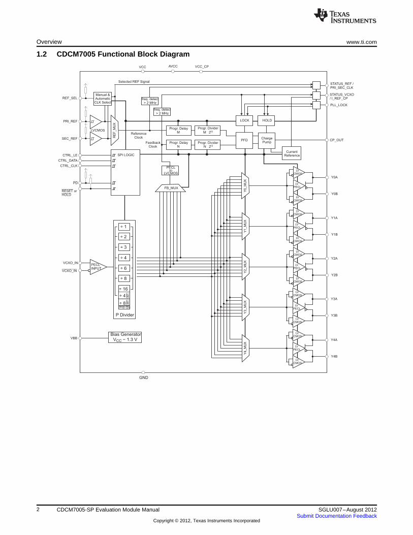
The CDCM7005 is a high-performance, low phase noise and low skew clock synchronizer thatsynchronizes an on-board voltage controlled crystal oscillator (VC(X)O) frequency to an external referenceclock. The device operates up to 2 GHz. The PLL loop bandwidth and damping factor can be adjusted tomeet different system requirements by selecting the external VC(X)O, loop filter components, frequencyfor PFD, and charge pump current. Each of the five differential LVPECL and five LVCMOS pair outputscan be programmed by a serial peripheral interface (SPI). The SPI allows individual control of thefrequency and enable/disable state of each output. As the system requires external components like aloop filter and VC(X)O, this EVM provides an easy method to evaluate and modify the performance andparameters of the clock system in conjunction with the specific customer application. Loop bandwidth canbe selected as low as 10 Hz or less, allowing the device to clean the system’s clock jitter.
In non PLL mode, the CDCM7005 can be used as a simple LVPECL or LVCMOS buffer with divideroptions.
1SGLU007–August 2012 CDCM7005-SP Evaluation Module ManualSubmit Documentation Feedback
Copyright © 2012, Texas Instruments Incorporated
PECLto
LVCMOS
Progr. DelayN
PECLINPUT
CTRL_LE
CTRL_DATA
CTRL_CLK
VCXO_IN
CP_OUT
PLL_LOCK
STATUS_REF /PRI_SEC_CLK
Bias GeneratorVBB
VCC_CPVCC AVCC
GND
PRI_REF
SEC_REF
REF_SEL
RE
F_M
UX
LVCMOS
FB_MUX
LVCMOS
Y0B
Y0A
LVCMOS
LVPECL
LVCMOS
Y1B
Y1A
LVCMOS
LVPECL
LVCMOS
Y2B
Y2A
LVCMOS
LVPECL
LVCMOS
Y3B
Y3A
LVCMOS
LVPECL
LVCMOS
Y4B
Y4A
LVCMOS
LVPECL
SPI LOGIC
Manual &AutomaticCLK Select
CurrentReference
ReferenceClock
freq. detect> 2 MHz
Selected REF Signal
Progr. DividerN 212
Y0_M
UX
P Divider
÷ 3
÷ 4
÷ 6
/8÷ 8
÷ 16
÷ 1
÷ 2
÷ 4
÷ 8
90
o90
o
LOCK
ChargePump
PFD
HOLD
Y1_M
UX
Y2_M
UX
Y3_
MU
XY
4_M
UX
P16−Div
freq. detect> 2 MHz
Progr. DelayM
Progr. Divider
M 210
FeedbackClock
VCC − 1.3 V
STATUS_VCXO/ I_REF_CP
VCXO_IN
RESET orHOLD
PD
Overview www.ti.com
1.2 CDCM7005 Functional Block Diagram
2 CDCM7005-SP Evaluation Module Manual SGLU007–August 2012Submit Documentation Feedback
Copyright © 2012, Texas Instruments Incorporated
www.ti.com Quick Start
2 Quick Start
In order to setup the EVM quickly and to take some measurements at default settings, the followingactions are required:
• Supply 3.3 V to P1, LED D4 will be on.
• Apply a single-ended reference clock to the reference clock input PRI_REF (pin A1) or SEC_REF (pinB1). For default setting, the reference clock must be 1/8th of the VC(X)O frequency. If REF_SEL is setto 1, then PRI_REF is selected. If REF_SEL is set to 0, then SEC_REF is selected. This selection canbe realized via J26 (header 1 and 2 is high; header 2 and 3 is low). The VCXO installed on the EVMis approximately 491.52 MHz. It may be necessary to adjust the 1/8 frequency applied to thereference clock by small amounts above or below 61.44 MHz to obtain lock.
• Connect Y0/Y0B (or Y1/Y1B) to oscilloscope in order to check an output signal. Ensure theoscilloscope has 50 Ω to ground termination.
After power up, D1 is on if there is a valid reference clock and D2 is on if there is a valid VC(X)O clock forthe CDCM7005. If D3 turns on, then the reference clock and the VC(X)O clocks are phase locked.
3SGLU007–August 2012 CDCM7005-SP Evaluation Module ManualSubmit Documentation Feedback
Copyright © 2012, Texas Instruments Incorporated
EVM Hardware www.ti.com
3 EVM Hardware
This chapter discusses the EVM hardware.
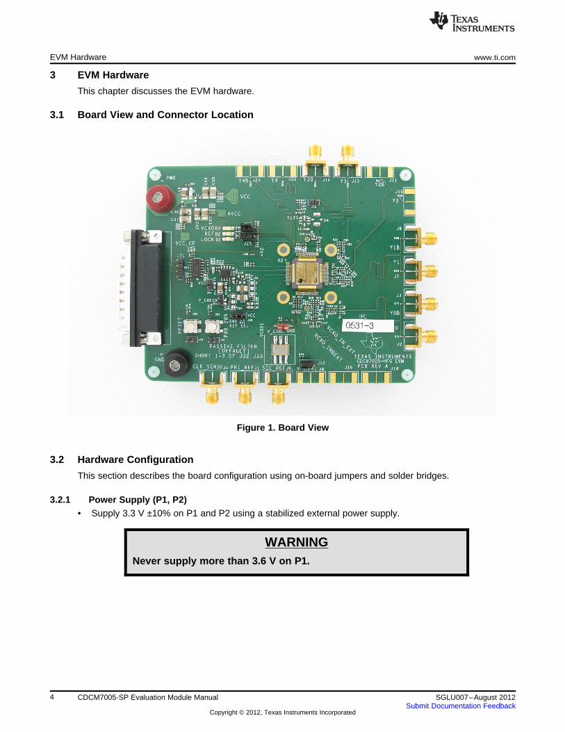
3.1 Board View and Connector Location
Figure 1. Board View
3.2 Hardware Configuration
This section describes the board configuration using on-board jumpers and solder bridges.
3.2.1 Power Supply (P1, P2)• Supply 3.3 V ±10% on P1 and P2 using a stabilized external power supply.
WARNINGNever supply more than 3.6 V on P1.
4 CDCM7005-SP Evaluation Module Manual SGLU007–August 2012Submit Documentation Feedback
Copyright © 2012, Texas Instruments Incorporated
www.ti.com EVM Hardware
3.2.2 Onboard Switches and Indicators (SW1−SW2, D1−D4)• Push SW1 to enter the power-down mode of the CDCM7005 device. Then all current sources are
switched off, all outputs are switched into 3-state, and all dividers (M, N, and P) are reset to default.
• Push SW2 to enter the reset mode of the device. The charge pump (CP) is switched to 3-state and allcounters (N, M, P) are rest to zero (the initial divider settings are maintained in SPI.
• The three status outputs of the CDCM7005 are fed to LED indicators. D1 on indicates a valid referenceinput clock signal. D2 is on if the VC(X)O input clock is valid and D3 turns on if the PLL has beenlocked.
• D4 indicates power supply.
NOTE: In case of a low input impedance of the VC(X)O control voltage input, there is a possibilityD3 may not turn on to indicate locking.
3.2.3 Programming Interfaces (J30, J31)
The SPI of the device is used for writing to the control register of the device. It consists of three controllines CTRL_CLK, CTRL_DATA, and CTRL_LE. There are four 30-bit wide RAM registers, which can beaddressed by the two LSBs of a transferred word. Every transmitted word must have 32 bits, starting withMSB. After supplying power or activating the power-down mode, the registers are loaded with the devicedefault values internally (see the CDCM7005 data sheet, SGLS390). However, if specific register settingsare required for any applications, there are two ways to program the device externally:
• Connect the parallel port cable to the PC and EVM parallel port. This needs control S/W (seeChapter 4).
3.2.4 Loop Filter (J32−J34)
The loop filter is one of the key elements determining the loop bandwidth of the PLL. The loop filterconverts the charge pump current into the control voltage for the voltage controlled oscillator. The phasedifference between the input clocks of the phase frequency detector determines the width of the chargepump output current pulses. These high frequency pulses are transformed into a voltage to control theoscillator.
Basically, two types of loop filters are implemented on the EVM.
• Passive loop filter
• External active loop filter using an external low-noise OPA
Filter types can be selected by soldering bridges J32−J34, see Table 1. Control voltage of the VC(X)O canbe measured at J9 or TP1. If an external OPA is used, it needs to be switched on by connecting J34. Forexample, passive filter operation is provided when pads 1 and 3 of J33 are solder bridged and pads 1 and3 of J32 are solder bridged.
Default setting: Passive Loop Filter
Table 1. Filter Configurations
BRIDGE PASSIVE FILTER ACTIVE WITH AN EXTERNAL OPA
J33 1-3 1-2
J34 Open Closed
J32 1-3 1-2
5SGLU007–August 2012 CDCM7005-SP Evaluation Module ManualSubmit Documentation Feedback
Copyright © 2012, Texas Instruments Incorporated
EVM Hardware www.ti.com
3.2.5 High-Speed Outputs and Inputs (J1−J4, J6−J11, J13, J14, J22, and J23)
The CDCM7005 drives five differential LVPECL outputs. All PECL outputs are ac-coupled and terminatedwith 150 Ω to GND. This is in contrast to typical LVPECL termination, which requires VCC − 2 V astermination voltage. The reason is to simplify the power supply scheme. The device output’s traceimpedance is 50 Ω and traces are matched in length. All outputs have options for pullup and pulldownresistors.
When the CDCM7005 is powered up, it defaults to five LVPECL outputs. However, this EVM is configuredas follows:
• Y0 − Y2 = LVPECL
• Y3, Y4 = LVCMOS (in addition Y4 has an option for a custom filter)
The reference input clock signal has to be applied to J1 or J6. The reference input clock signal can besensed on J4. In this case, close the bridge J5 (the oscilloscope’s 50 Ω may be used to terminate the50-Ω trace). The reference input clock sense line is matched to the LVPECL outputs line to avoid anyadditional delay offset. The input is ac-coupled (C4).
3.2.6 VC(X)O Inputs and Outputs (J16−J18)
The CDCM7005 requires an external VC(X)O in order to complete the PLL loop. The VC(X)O adjusts thefrequency and phase depending on the control voltage level coming from the loop filter and provide theinput clock to the LVPECL block.
Another option would be to use an external source via J16 and J18.
3.2.7 AC-Coupling at PRI_REF (C1, R4, R6) and SEC_REF (C5, R13, R15)
An ac-coupling is provided at PRI_REF and SEC_REF to ease the use of the CDCM7005 with differentsignaling levels (LVCMOS, LVPECL, LVDS). However, the ac-coupling will increase the PLL stabilizationtime after power up due to transient effects. It also increases the switching time between PRI_REF andSEC_REF in case of automatic reference clock switching. Therefore, the ac-coupling must be removed foroptimized system performance (C1 and C5 has to be replaced with a 0-Ω resistor and R4, R6, R13, andR15 have to be removed).
6 CDCM7005-SP Evaluation Module Manual SGLU007–August 2012Submit Documentation Feedback
Copyright © 2012, Texas Instruments Incorporated
www.ti.com Serial Peripheral Interface (SPI) Software
4 Serial Peripheral Interface (SPI) Software
This chapter discusses the serial peripheral interface software.
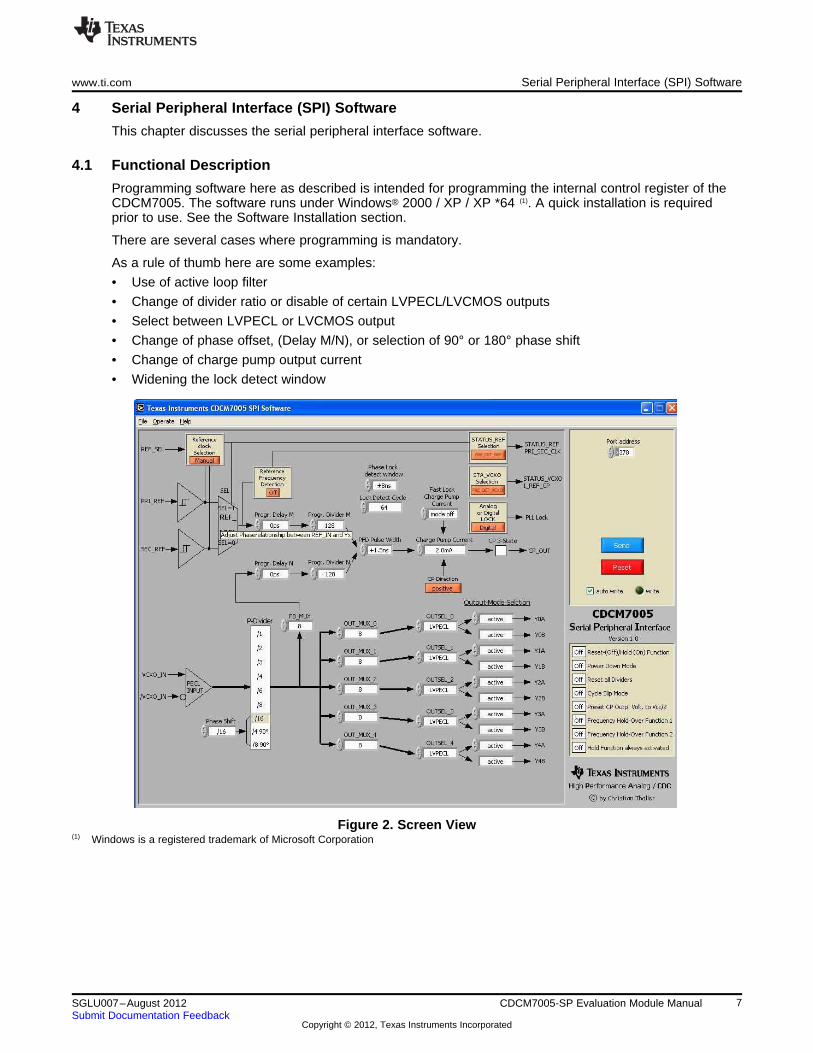
4.1 Functional Description
Programming software here as described is intended for programming the internal control register of theCDCM7005. The software runs under Windows® 2000 / XP / XP *64 (1). A quick installation is requiredprior to use. See the Software Installation section.
There are several cases where programming is mandatory.
As a rule of thumb here are some examples:
• Use of active loop filter
• Change of divider ratio or disable of certain LVPECL/LVCMOS outputs
• Select between LVPECL or LVCMOS output
• Change of phase offset, (Delay M/N), or selection of 90° or 180° phase shift
• Change of charge pump output current
• Widening the lock detect window
Figure 2. Screen View(1) Windows is a registered trademark of Microsoft Corporation
7SGLU007–August 2012 CDCM7005-SP Evaluation Module ManualSubmit Documentation Feedback
Copyright © 2012, Texas Instruments Incorporated
Serial Peripheral Interface (SPI) Software www.ti.com
4.2 Software Installation
Follow the steps below in order to install the SPI control software:
1. Download the CDCM7005 SPI Software from the TI Website (www.ti.com)
2. Run program setup.exe
3. Reboot your computer
4. Run the software from Start → Programs → CDCM7005 SPI
8 CDCM7005-SP Evaluation Module Manual SGLU007–August 2012Submit Documentation Feedback
Copyright © 2012, Texas Instruments Incorporated
SPI
PECL_OUT_B
PECL_OUT
V_CTRL
VC(X)O
CP_OUT
VC(X)O_IN
VC(X)O_IN_B
CTRL_LECTRL_DATACTRL_CLK
PRI_REF
YnB
YnA
CDCM7005
PLL_LOCK
STATUS_VC(X)O
STATUS_REF
Low-Pass Filter
R14.7 kΩ
C3
100 nF
R2160 Ω
C2
100 nFC122 µF
10 nF10 nF
10 nF
R150 Ω
R150 Ω
R82 Ω
R82 Ω
130 Ω
VCC VCC
130 Ω
SEC_REF
491.52 MHz
www.ti.com Application Circuit Diagram
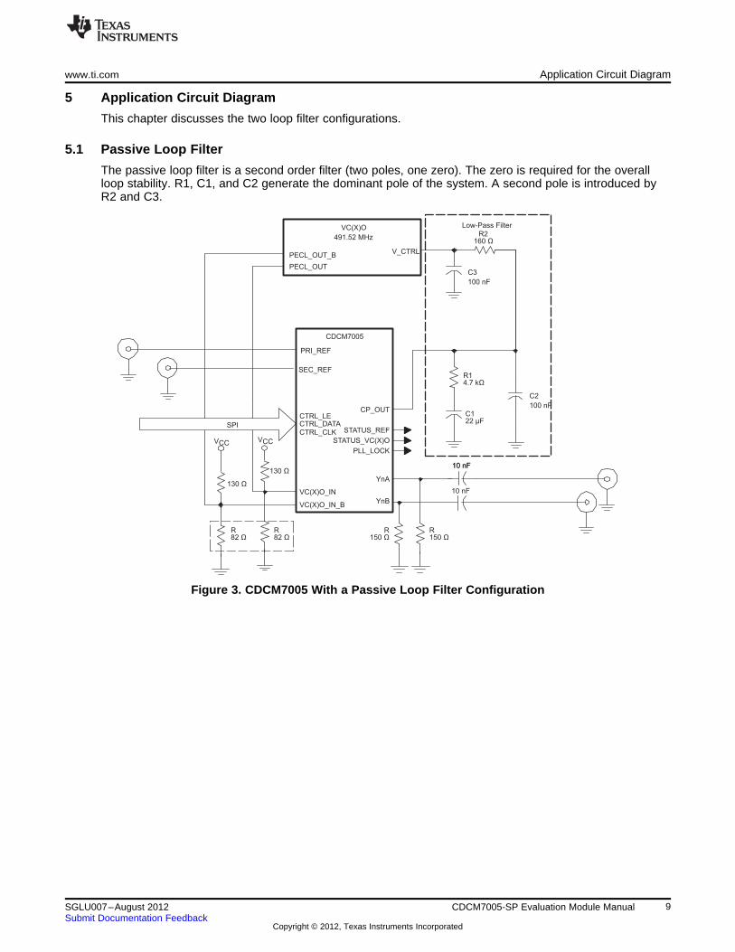
5 Application Circuit Diagram
This chapter discusses the two loop filter configurations.
5.1 Passive Loop Filter
The passive loop filter is a second order filter (two poles, one zero). The zero is required for the overallloop stability. R1, C1, and C2 generate the dominant pole of the system. A second pole is introduced byR2 and C3.
Figure 3. CDCM7005 With a Passive Loop Filter Configuration
9SGLU007–August 2012 CDCM7005-SP Evaluation Module ManualSubmit Documentation Feedback
Copyright © 2012, Texas Instruments Incorporated
SPI
PECL_OUT_B
PECL_OUT
V_CTRL
VC(X)O
CP_OUT
CTRL_LE
CTRL_DATA
CTRL_CLK
CDCM7005
PLL_LOCK
STATUS_REFSTATUS_VC(X)O
Vcc
Low-Pass Filter
Vcc
InP
InN
OutOPA341
R82 Ω R
82 Ω
R150 Ω
R150 Ω
10 nF
10 nF
C1100 nF
R1180 Ω
C1
100 nF
R610 kΩ
R510 kΩ
C210 µF
R310 kΩ
C3
100 nF
130 Ω
VCC
130 Ω
VCC
PRI_REF
SEC_REF
R24.7 kΩ
YnB
YnA
VC(X)O_IN
VC(X)O_IN
491.52 MHz
Application Circuit Diagram www.ti.com
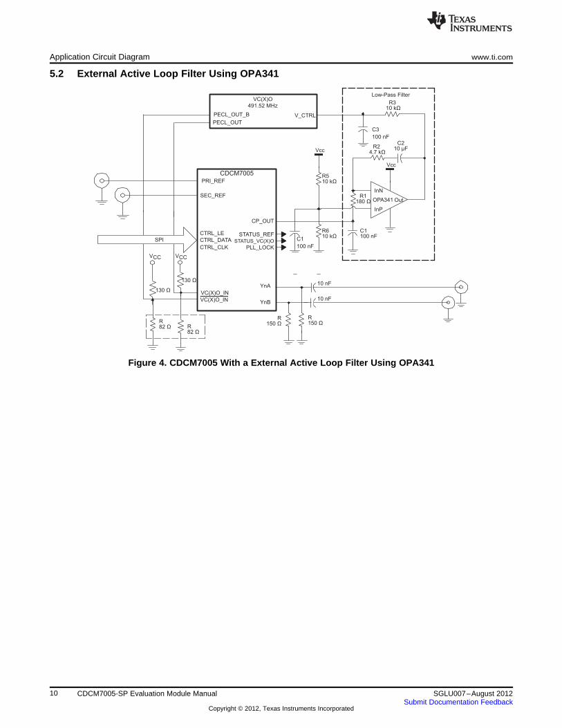
5.2 External Active Loop Filter Using OPA341
Figure 4. CDCM7005 With a External Active Loop Filter Using OPA341
10 CDCM7005-SP Evaluation Module Manual SGLU007–August 2012Submit Documentation Feedback
Copyright © 2012, Texas Instruments Incorporated
www.ti.com Board Layout
6 Board Layout
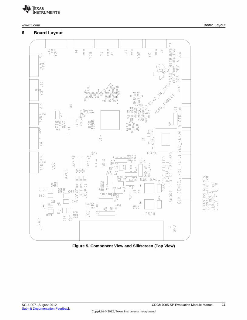
Figure 5. Component View and Silkscreen (Top View)
11SGLU007–August 2012 CDCM7005-SP Evaluation Module ManualSubmit Documentation Feedback
Copyright © 2012, Texas Instruments Incorporated
Board Layout www.ti.com
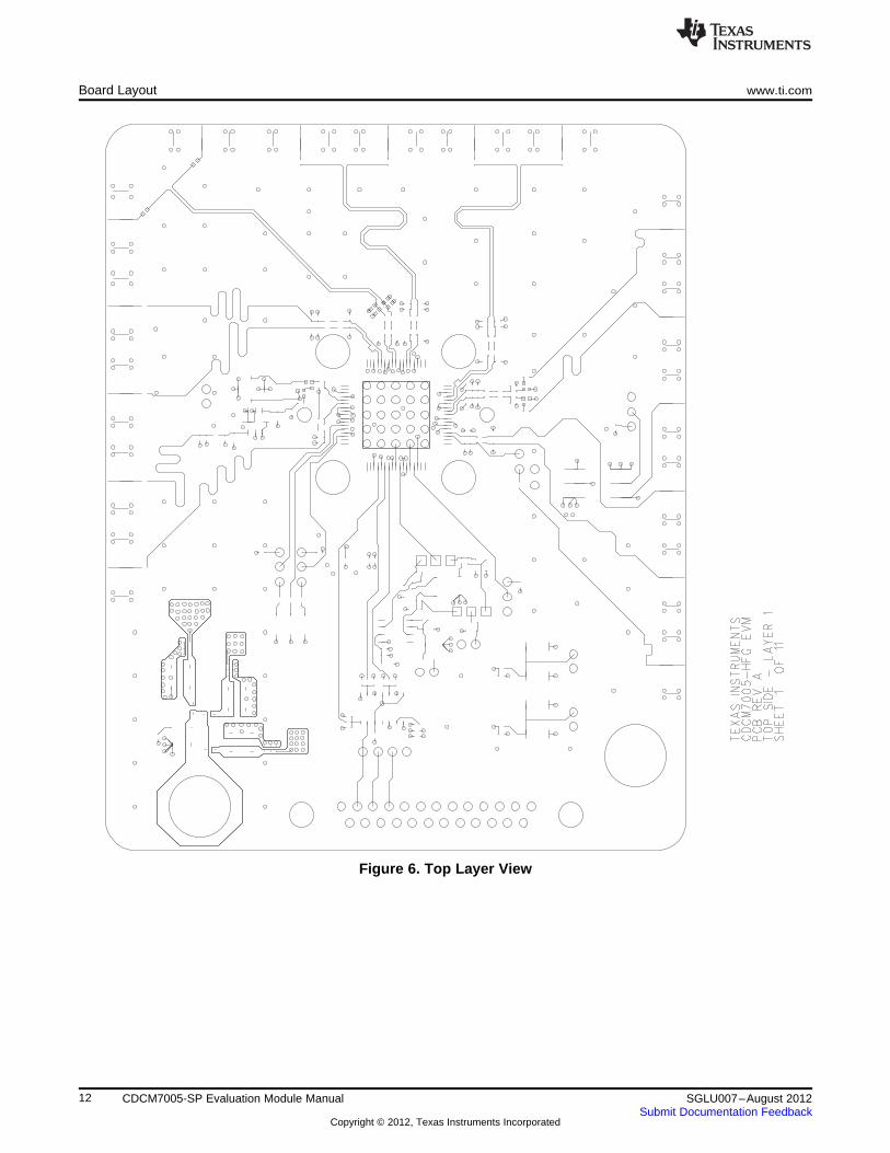
Figure 6. Top Layer View
12 CDCM7005-SP Evaluation Module Manual SGLU007–August 2012Submit Documentation Feedback
Copyright © 2012, Texas Instruments Incorporated
www.ti.com Board Layout
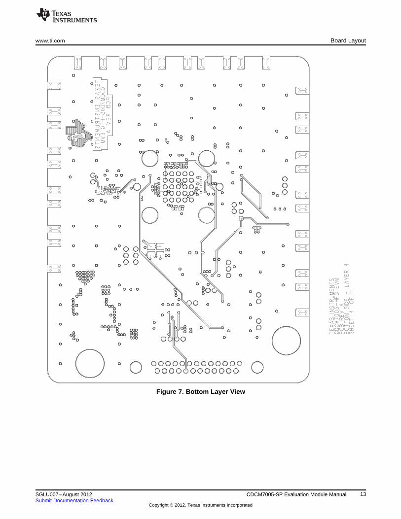
Figure 7. Bottom Layer View
13SGLU007–August 2012 CDCM7005-SP Evaluation Module ManualSubmit Documentation Feedback
Copyright © 2012, Texas Instruments Incorporated
Board Layout www.ti.com
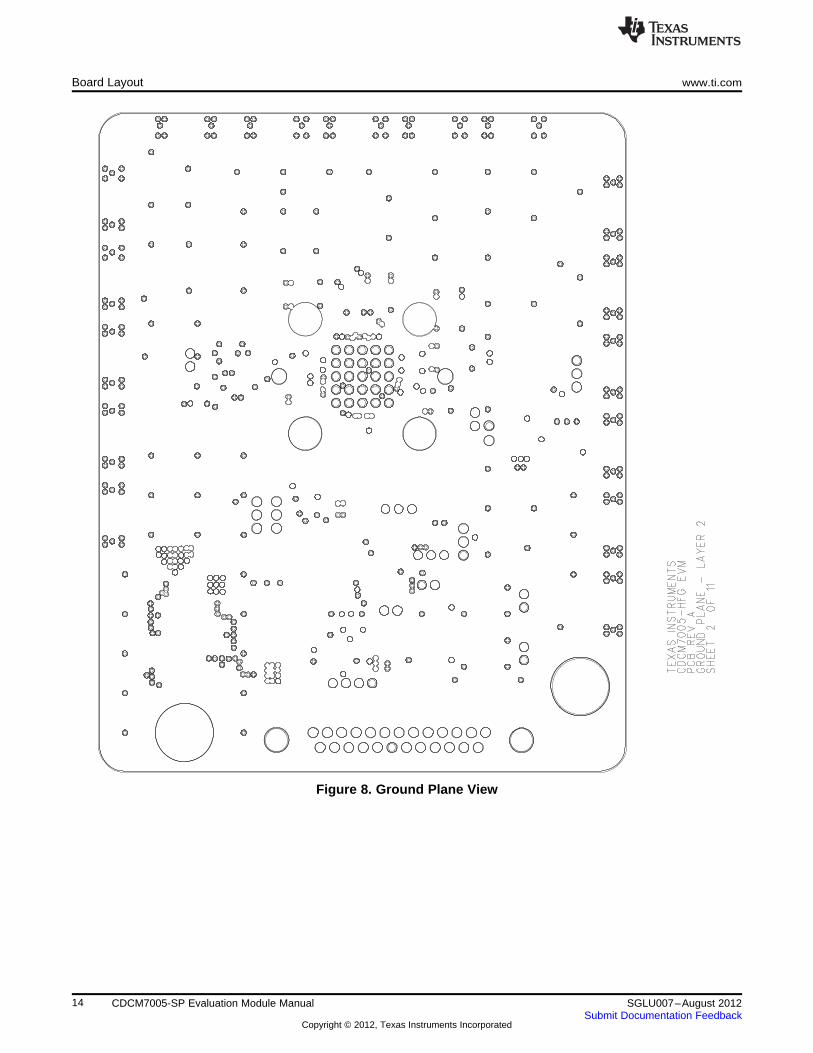
Figure 8. Ground Plane View
14 CDCM7005-SP Evaluation Module Manual SGLU007–August 2012Submit Documentation Feedback
Copyright © 2012, Texas Instruments Incorporated
www.ti.com Board Layout
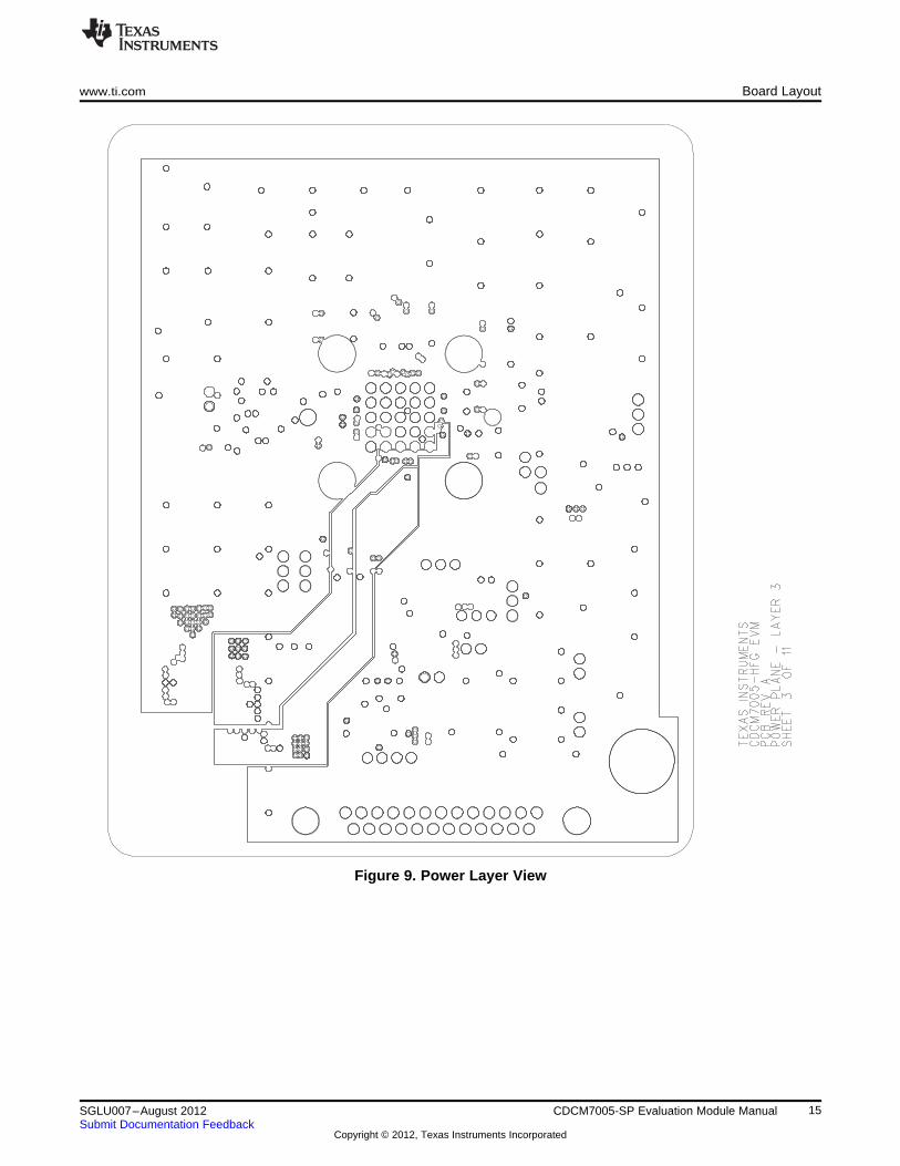
Figure 9. Power Layer View
15SGLU007–August 2012 CDCM7005-SP Evaluation Module ManualSubmit Documentation Feedback
Copyright © 2012, Texas Instruments Incorporated

Schematics www.ti.com
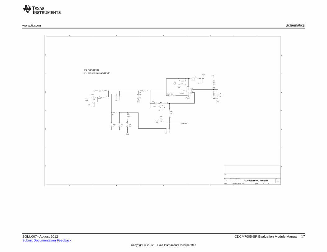
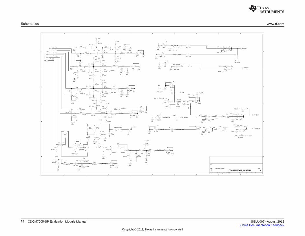
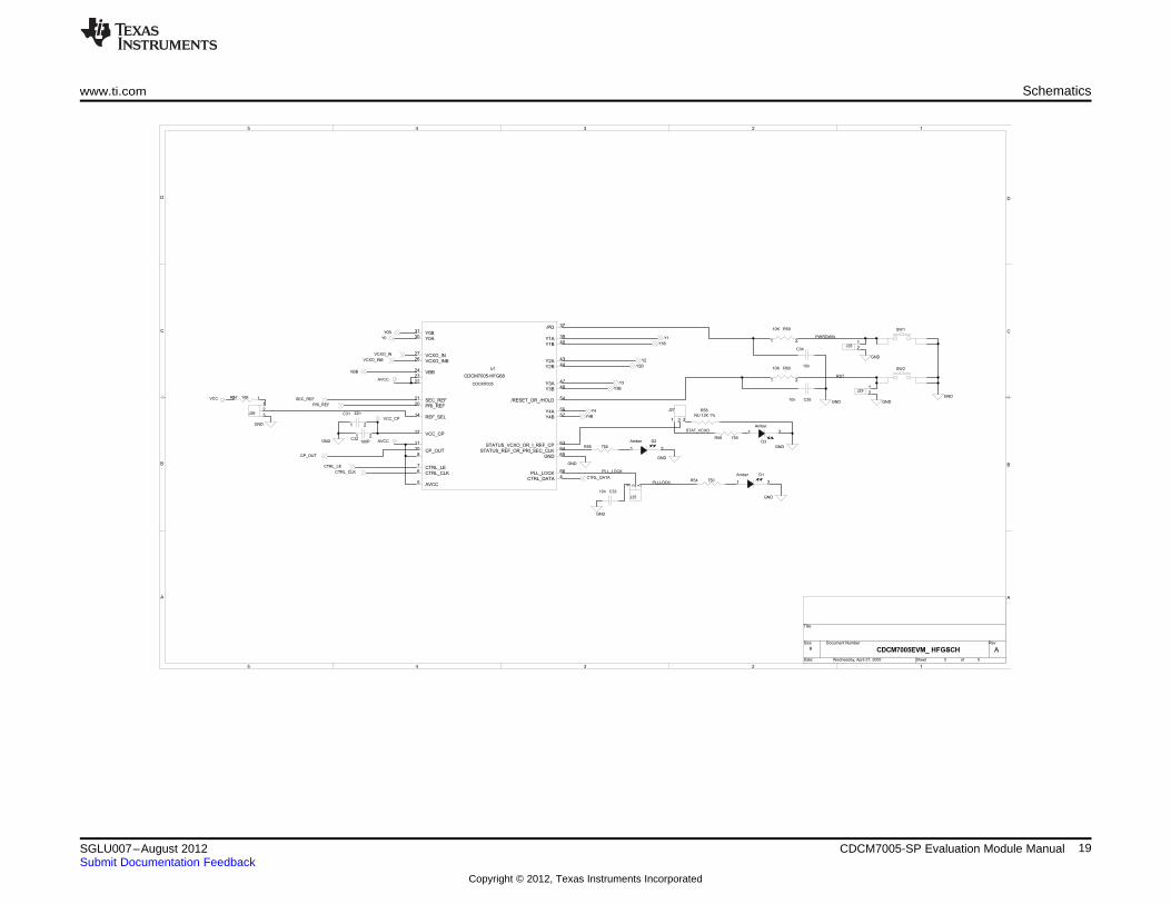
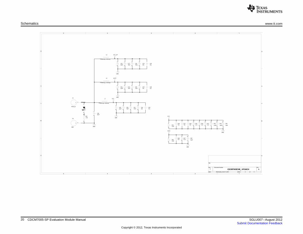
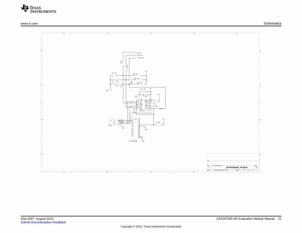
7 Schematics
See the following pages for the CDCM7005 schematics.
16 CDCM7005-SP Evaluation Module Manual SGLU007–August 2012Submit Documentation Feedback
Copyright © 2012, Texas Instruments Incorporated
Thursday, May 05, 2005
B CDCM7005EVM_ HFG-SCH A
1 5ofSheetDate:
RevDocument NumberSize
Title
016 !"#$%$&'%$$
()*+, 016-!(.! !"#&%$&'%$$'%$/
A
B
C
D
5 4 3 2 1
D
C
B
A
12345
1 2R51
100K
12
J34
12
C28
.1uF
12
C74
10uF
12
C80
.1uF
12 C76
.1uF
12C77
10uF
12
R75
10K
12
C29
.1uF
12
R73
180
12
C75
.1uF
1 2R52
160
12
C30
22uF
213
J32
12R71 10K
1 2R70
10K
12
C27
.1uF
12C78
NU
1 2R72
4.7K
12
R74
10K
12
J24
12
R53
4.7K
+
-
63
2
748 1
5
U5
OPA341
L8
2.2nH
12
C79
.1uF
213
J33
GND
GND
VCC
GND
GND
GND
VCC
GND
GND
V_CTRL
CP_OUT
V_CTRL
www.ti.com Schematics
17SGLU007–August 2012 CDCM7005-SP Evaluation Module ManualSubmit Documentation Feedback
Copyright © 2012, Texas Instruments Incorporated
Wednesday, May 11, 2005
B
52
ACDCM7005EVM_ HFG-SCH
ofSheetDate:
RevDocument NumberSize
Title
A
B
C
D
5 4 3 2 1
D
C
B
A
12345
1 2
R95
0 ohm
12
R49
NU 150
12
R35 NU 100
12
R8
150
TP1
12R38 130
1 2
J19
12R34
0 ohm
1 IN
5OUT
FLT1
** TS-38S
1 2R15
100
1 2
J5
HEADER 2
1 2
R12 NU
1 2
3
J3
SMA
C2 10n
1 2
R79
22 ohm
1 2
3
J8
SMA
1 2C11
100P
12R36 82
1 2
C21 ** 10n
1 2R6
100
1 2R4
100
12
R17
150
C17
10n
1 2
R88
0 ohm
12
R40
** 62
12
R5
150
12
3
J21
12
L4
** 180nH
12R43 82
1 2
R84
0 ohm
1 2
3
J11
NU_SMAC9 10n
1 2
3
J7
SMA
1 2
R82
0 ohm
1 2
R85
0 ohm
12R45
NU 0 ohm
TP2
12R41
0 ohm
12
R37 NU
1 2
R93
0 ohm
C1 10n
1 2
R83
0 ohm
12
R22
NU 100
1 2
R87
0 ohm
12
R20
NU 100
C13 10n
12
R26
NU 100
12
R47
** NU 100
12
3J12
12R25 10K
12R42
0 ohm
1 2
R76
0 ohm
12
C24** 22pF
1 2
R28
NU 0 ohm
12
3
J9
NU_SMA
C7 10n
1 2
R91
0 ohm
1 2
R48
NU 100
12
C18
** 1000pF
1 2
3
J14
NU_SMA
12
3
J16
NU_SMA
1 2
C10 100n
C5 10n
12
R9
NU 100
1 2
C22
** .1uF
1 2
R81
22 ohm
1 2
3
J10
NU_SMA
12
R30
NU 100
C3 10n
12
R1
NU 100
C15
10n
1 2
C14
0 ohm
12R31 130
12
R80
NU 150
C26 10n
12
R23
150
12
R16
NU 100
1 2
R86
0 ohm
1 2L1
** 75 ohm@100MHz
12
R32
NU 150
12
R7
NU 100
1 2
R89
0 ohm1
2
R21
150
1 2R13
100
1 2
R94
0 ohm
1 2
R3 NU
12
3
J1
SMA
12
R24
NU 100
12R50
NU 100
12
3
J18
NU_SMA
1 2
3
J22
NU_SMA
12
R11
NU 100
12
3
J4SMA
12
R19
NU 100
12
R29
NU 150
12
R46
** NU 100
1 2
R78
22 ohm
12
C23
** NU 1.1pF
12
C25
** NU 1pF
12
R14
150
3
24
1
U4
SGA-4586
12
3
J17
1 2
R77
0 ohm
12
R39
** 62
12
R2NU 100
12
R44 NU
12
C19
** 1uF12
L2
** 470nH
12
3
J20
C8 10n
1 2
3
J2
SMA
C4 10n
1 2
R92
0 ohm
C12 10n
12
3
J6
SMA
1 2
3
J23
NU_SMA
12
** 180nH
C6 10n
1 2C16
0 ohm
12
R10
NU 100
1 V_CTRL2 EN3 GND 4OUT
5OUTB
6VCC
VCXO1
VCXO_61
2R27
NU 100
12
3
J15
1 2
R90
0 ohm
12
R18
NU 100
1 2
3
J13
NU_SMA
12R33
0 ohm
12
C20
** .1uF
GND
GND
GND
GND
GND
VCC
GND
GND
GND
VCC
GND
GND
GND
VCC
GND
GND
GND
GND
GND
GND
GND
GND
GND
GND
GND
GND
GND
GND
GND
GND
GND
GND
GND
VCC
GND
GND
GND
GND
GND
GND
GND
VCC
GND
GND
GND
GND
GND
VCC
GND
VCC
GND
GND
VCC
VCC
VCC
VCC
VCC
VCC
VCC
VCC
VCC
VCC
GND
GND
GND
GND
V_CTRL
Y0
Y0B
Y1
Y3
Y4
Y2
Y1B
Y2B
Y3B
Y4B
PRI_REF
SEC_REF
VCXO_INB
VCXO_IN
VBB
VBB
SEC_REFCLK
PRI_REFCLK
VCXO_INB_EXT
OU
TB
VCXO_IN_SMA
VCXO_IN_EXT VCXO_INB_SMA
OU
T
V_CTRL
PRI_CLK_SENSE
Y0B_SMA
Y0_SMA
Y1_SMA
Y1B_SMA
Y2_SMA
Y2B_SMA
Y4_SMA
Y4B_SMA
Y3B_SMA
Y3_SMA
Schematics www.ti.com
18 CDCM7005-SP Evaluation Module Manual SGLU007–August 2012Submit Documentation Feedback
Copyright © 2012, Texas Instruments Incorporated
Wednesday, April 27, 2005
B CDCM7005EVM_ HFG-SCH A
3 5ofSheetDate:
RevDocument NumberSize
Title
A
B
C
D
5 4 3 2 1
D
C
B
A
12345
SW1
R54 750
1 2 3
J25
12R57 10K
1 2
D3
Amber
1 2
D2Amber
12J29
1 2
R5910K
1 2
D1Amber
C34
10n
1 2
C31 22n
123J26
1 2 3
J27 R58NU 12K 1%
SW2
1 2
R6010K
C3310n
1 2C32
100P
12J28
R56 750
R55 750
C3510n
44Y2B
43Y2A
12 VCC_CP
11
48Y3B
47Y3A
14 REF_SEL
2322
21 SEC_REF20 PRI_REF
27 VCXO_IN26 VCXO_INB
24 VBB
54/RESET_OR_/HOLD
56Y4A57Y4B
37/PD
39Y1A40Y1B
63STATUS_VCXO_OR_I_REF_CP64STATUS_REF_OR_PRI_SEC_CLK65GND
66PLL_LOCK4CTRL_DATA
5 AVCC
6 CTRL_CLK
7 CTRL_LE
810 CP_OUT
30 Y0A
31 Y0B
U1
CDCM7005-HFG68
CDCM7005
GND
VCC_CP
AVCC
AVCC
VCC
GND
GND
GND
GND
GND
GND
GND
GND
GND
GND
CP_OUT
CTRL_LE
CTRL_CLK
CTRL_DATA
PRI_REF
SEC_REF
VBB
VCXO_IN
VCXO_INB
Y4
Y4B
Y3
Y3B
Y2
Y2B
Y1
Y1B
Y0B
Y0 PWRDWN
RST
PLLLOCK
PLL_LOCK
STAT_VCXO
www.ti.com Schematics
19SGLU007–August 2012 CDCM7005-SP Evaluation Module ManualSubmit Documentation Feedback
Copyright © 2012, Texas Instruments Incorporated
Wednesday, April 27, 2005
B CDCM7005EVM_ HFG-SCH A
4 5ofSheetDate:
RevDocument NumberSize
Title
A
B
C
D
5 4 3 2 1
D
C
B
A
12345
12
C63
100P
C53
10n
C66
10n
12
C38
100n
12
C59
2.2n
C57
10n
C46
10n
12
C37
10uF
12
C65
10uF
12
C48
22uF
1 2
L5
75 OHM @ 100MHZ
12
C52
33n
11
P1
PWR_IN
12
C60
2.2n
12
C64
100P
12
C67
2.2n
11
P2
GND
12
D4
GREEN
12
C45
33n
12
C61
2.2n1
2
C43
10uF
12
C42
22uF
C40
10n
12
C51
100n
C58
10n
12
C50
10uF
1 2
L7
75 OHM @ 100MHZ
12
C68
100P
12
R61
1.5K
12
C44
100n
12
C62
100P
12
C39
33n
12
C36
22uF
12
C55
10uF
12
C49
22uF
1 2
L6
75 OHM @ 100MHZ
C56
10n
VCC
GND
AVCC
GND
GND
AVCC
GND
GND
VCC
GND
VCC_CP
PWR_IN
Schematics www.ti.com
20 CDCM7005-SP Evaluation Module Manual SGLU007–August 2012Submit Documentation Feedback
Copyright © 2012, Texas Instruments Incorporated
Wednesday, April 27, 2005
B
55
ACDCM7005EVM_ HFG-SCH
ofSheetDate:
RevDocument NumberSize
Title
A
B
C
D
5 4 3 2 1
D
C
B
A
12345
12R64 100K
1 2C73
100P
12R66 100K
1 142 153 164 175 186 197 208 219 22
10 2311 2412 2513 26
27
J30
PARALLEL PORT
1 2
C69 10p
1234
J31
HDR4
12R67 100K
12
R63
100
1 2C70 10p
3 1Y4 2 OE5 2A6 2Y
1 1 OE134 OE
114Y103 OE93A83Y
14VCC
7 GND
124A
2 1A
U3SN74LV125
1 2
R6910K1
2
R62
100
12R68 10K
12
R65
100
1 2
C72 100n
1 2C71 10p
GND
GND
GND
VCC
GND
GND
GND
VCC
GND
VCC
VCC
CTRL_LE
CTRL_DATA
CTRL_CLK
SPI_CLK
SPI_LE
SPI_DATA
LE
CLK
DATA
www.ti.com Schematics
21SGLU007–August 2012 CDCM7005-SP Evaluation Module ManualSubmit Documentation Feedback
Copyright © 2012, Texas Instruments Incorporated
22 CDCM7005-SP Evaluation Module Manual SGLU007–August 2012Submit Documentation Feedback
EVALUATION BOARD/KIT/MODULE (EVM) ADDITIONAL TERMS
Texas Instruments (TI) provides the enclosed Evaluation Board/Kit/Module (EVM) under the following conditions:
The user assumes all responsibility and liability for proper and safe handling of the goods. Further, the user indemnifies TI from all claimsarising from the handling or use of the goods.
Should this evaluation board/kit not meet the specifications indicated in the User’s Guide, the board/kit may be returned within 30 days fromthe date of delivery for a full refund. THE FOREGOING LIMITED WARRANTY IS THE EXCLUSIVE WARRANTY MADE BY SELLER TOBUYER AND IS IN LIEU OF ALL OTHER WARRANTIES, EXPRESSED, IMPLIED, OR STATUTORY, INCLUDING ANY WARRANTY OFMERCHANTABILITY OR FITNESS FOR ANY PARTICULAR PURPOSE. EXCEPT TO THE EXTENT OF THE INDEMNITY SET FORTHABOVE, NEITHER PARTY SHALL BE LIABLE TO THE OTHER FOR ANY INDIRECT, SPECIAL, INCIDENTAL, OR CONSEQUENTIALDAMAGES.
Please read the User's Guide and, specifically, the Warnings and Restrictions notice in the User's Guide prior to handling the product. Thisnotice contains important safety information about temperatures and voltages. For additional information on TI's environmental and/or safetyprograms, please visit www.ti.com/esh or contact TI.
No license is granted under any patent right or other intellectual property right of TI covering or relating to any machine, process, orcombination in which such TI products or services might be or are used. TI currently deals with a variety of customers for products, andtherefore our arrangement with the user is not exclusive. TI assumes no liability for applications assistance, customer product design,software performance, or infringement of patents or services described herein.
REGULATORY COMPLIANCE INFORMATION
As noted in the EVM User’s Guide and/or EVM itself, this EVM and/or accompanying hardware may or may not be subject to the FederalCommunications Commission (FCC) and Industry Canada (IC) rules.
For EVMs not subject to the above rules, this evaluation board/kit/module is intended for use for ENGINEERING DEVELOPMENT,DEMONSTRATION OR EVALUATION PURPOSES ONLY and is not considered by TI to be a finished end product fit for general consumeruse. It generates, uses, and can radiate radio frequency energy and has not been tested for compliance with the limits of computingdevices pursuant to part 15 of FCC or ICES-003 rules, which are designed to provide reasonable protection against radio frequencyinterference. Operation of the equipment may cause interference with radio communications, in which case the user at his own expense willbe required to take whatever measures may be required to correct this interference.
General Statement for EVMs including a radio
User Power/Frequency Use Obligations: This radio is intended for development/professional use only in legally allocated frequency andpower limits. Any use of radio frequencies and/or power availability of this EVM and its development application(s) must comply with locallaws governing radio spectrum allocation and power limits for this evaluation module. It is the user’s sole responsibility to only operate thisradio in legally acceptable frequency space and within legally mandated power limitations. Any exceptions to this are strictly prohibited andunauthorized by Texas Instruments unless user has obtained appropriate experimental/development licenses from local regulatoryauthorities, which is responsibility of user including its acceptable authorization.
For EVMs annotated as FCC – FEDERAL COMMUNICATIONS COMMISSION Part 15 Compliant
Caution
This device complies with part 15 of the FCC Rules. Operation is subject to the following two conditions: (1) This device may not causeharmful interference, and (2) this device must accept any interference received, including interference that may cause undesired operation.
Changes or modifications not expressly approved by the party responsible for compliance could void the user's authority to operate theequipment.
FCC Interference Statement for Class A EVM devices
This equipment has been tested and found to comply with the limits for a Class A digital device, pursuant to part 15 of the FCC Rules.These limits are designed to provide reasonable protection against harmful interference when the equipment is operated in a commercialenvironment. This equipment generates, uses, and can radiate radio frequency energy and, if not installed and used in accordance with theinstruction manual, may cause harmful interference to radio communications. Operation of this equipment in a residential area is likely tocause harmful interference in which case the user will be required to correct the interference at his own expense.
FCC Interference Statement for Class B EVM devices
This equipment has been tested and found to comply with the limits for a Class B digital device, pursuant to part 15 of the FCC Rules.These limits are designed to provide reasonable protection against harmful interference in a residential installation. This equipmentgenerates, uses and can radiate radio frequency energy and, if not installed and used in accordance with the instructions, may causeharmful interference to radio communications. However, there is no guarantee that interference will not occur in a particular installation. Ifthis equipment does cause harmful interference to radio or television reception, which can be determined by turning the equipment off andon, the user is encouraged to try to correct the interference by one or more of the following measures:
• Reorient or relocate the receiving antenna.• Increase the separation between the equipment and receiver.• Connect the equipment into an outlet on a circuit different from that to which the receiver is connected.• Consult the dealer or an experienced radio/TV technician for help.
For EVMs annotated as IC – INDUSTRY CANADA Compliant
This Class A or B digital apparatus complies with Canadian ICES-003.
Changes or modifications not expressly approved by the party responsible for compliance could void the user’s authority to operate theequipment.
Concerning EVMs including radio transmitters
This device complies with Industry Canada licence-exempt RSS standard(s). Operation is subject to the following two conditions: (1) thisdevice may not cause interference, and (2) this device must accept any interference, including interference that may cause undesiredoperation of the device.
Concerning EVMs including detachable antennas
Under Industry Canada regulations, this radio transmitter may only operate using an antenna of a type and maximum (or lesser) gainapproved for the transmitter by Industry Canada. To reduce potential radio interference to other users, the antenna type and its gain shouldbe so chosen that the equivalent isotropically radiated power (e.i.r.p.) is not more than that necessary for successful communication.
This radio transmitter has been approved by Industry Canada to operate with the antenna types listed in the user guide with the maximumpermissible gain and required antenna impedance for each antenna type indicated. Antenna types not included in this list, having a gaingreater than the maximum gain indicated for that type, are strictly prohibited for use with this device.
Cet appareil numérique de la classe A ou B est conforme à la norme NMB-003 du Canada.
Les changements ou les modifications pas expressément approuvés par la partie responsable de la conformité ont pu vider l’autorité del'utilisateur pour actionner l'équipement.
Concernant les EVMs avec appareils radio
Le présent appareil est conforme aux CNR d'Industrie Canada applicables aux appareils radio exempts de licence. L'exploitation estautorisée aux deux conditions suivantes : (1) l'appareil ne doit pas produire de brouillage, et (2) l'utilisateur de l'appareil doit accepter toutbrouillage radioélectrique subi, même si le brouillage est susceptible d'en compromettre le fonctionnement.
Concernant les EVMs avec antennes détachables
Conformément à la réglementation d'Industrie Canada, le présent émetteur radio peut fonctionner avec une antenne d'un type et d'un gainmaximal (ou inférieur) approuvé pour l'émetteur par Industrie Canada. Dans le but de réduire les risques de brouillage radioélectrique àl'intention des autres utilisateurs, il faut choisir le type d'antenne et son gain de sorte que la puissance isotrope rayonnée équivalente(p.i.r.e.) ne dépasse pas l'intensité nécessaire à l'établissement d'une communication satisfaisante.
Le présent émetteur radio a été approuvé par Industrie Canada pour fonctionner avec les types d'antenne énumérés dans le manueld’usage et ayant un gain admissible maximal et l'impédance requise pour chaque type d'antenne. Les types d'antenne non inclus danscette liste, ou dont le gain est supérieur au gain maximal indiqué, sont strictement interdits pour l'exploitation de l'émetteur.
SPACER
SPACER
SPACER
SPACER
SPACER
SPACER
SPACER
SPACER
【【Important Notice for Users of this Product in Japan】】This development kit is NOT certified as Confirming to Technical Regulations of Radio Law of Japan
If you use this product in Japan, you are required by Radio Law of Japan to follow the instructions below with respect to this product:
1. Use this product in a shielded room or any other test facility as defined in the notification #173 issued by Ministry of Internal Affairs andCommunications on March 28, 2006, based on Sub-section 1.1 of Article 6 of the Ministry’s Rule for Enforcement of Radio Law ofJapan,
2. Use this product only after you obtained the license of Test Radio Station as provided in Radio Law of Japan with respect to thisproduct, or
3. Use of this product only after you obtained the Technical Regulations Conformity Certification as provided in Radio Law of Japan withrespect to this product. Also, please do not transfer this product, unless you give the same notice above to the transferee. Please notethat if you could not follow the instructions above, you will be subject to penalties of Radio Law of Japan.
Texas Instruments Japan Limited(address) 24-1, Nishi-Shinjuku 6 chome, Shinjuku-ku, Tokyo, Japan
http://www.tij.co.jp
【ご使用にあたっての注】
本開発キットは技術基準適合証明を受けておりません。
本製品のご使用に際しては、電波法遵守のため、以下のいずれかの措置を取っていただく必要がありますのでご注意ください。1. 電波法施行規則第6条第1項第1号に基づく平成18年3月28日総務省告示第173号で定められた電波暗室等の試験設備でご使用いただく。2. 実験局の免許を取得後ご使用いただく。3. 技術基準適合証明を取得後ご使用いただく。
なお、本製品は、上記の「ご使用にあたっての注意」を譲渡先、移転先に通知しない限り、譲渡、移転できないものとします。
上記を遵守頂けない場合は、電波法の罰則が適用される可能性があることをご留意ください。
日本テキサス・インスツルメンツ株式会社東京都新宿区西新宿6丁目24番1号西新宿三井ビルhttp://www.tij.co.jp
SPACER
SPACER
SPACER
SPACER
SPACER
SPACER
SPACER
SPACER
SPACER
SPACER
SPACER
SPACER
SPACER
SPACER
SPACER
SPACER
EVALUATION BOARD/KIT/MODULE (EVM)WARNINGS, RESTRICTIONS AND DISCLAIMERS
For Feasibility Evaluation Only, in Laboratory/Development Environments. Unless otherwise indicated, this EVM is not a finishedelectrical equipment and not intended for consumer use. It is intended solely for use for preliminary feasibility evaluation inlaboratory/development environments by technically qualified electronics experts who are familiar with the dangers and application risksassociated with handling electrical mechanical components, systems and subsystems. It should not be used as all or part of a finished endproduct.
Your Sole Responsibility and Risk. You acknowledge, represent and agree that:
1. You have unique knowledge concerning Federal, State and local regulatory requirements (including but not limited to Food and DrugAdministration regulations, if applicable) which relate to your products and which relate to your use (and/or that of your employees,affiliates, contractors or designees) of the EVM for evaluation, testing and other purposes.
2. You have full and exclusive responsibility to assure the safety and compliance of your products with all such laws and other applicableregulatory requirements, and also to assure the safety of any activities to be conducted by you and/or your employees, affiliates,contractors or designees, using the EVM. Further, you are responsible to assure that any interfaces (electronic and/or mechanical)between the EVM and any human body are designed with suitable isolation and means to safely limit accessible leakage currents tominimize the risk of electrical shock hazard.
3. You will employ reasonable safeguards to ensure that your use of the EVM will not result in any property damage, injury or death, evenif the EVM should fail to perform as described or expected.
4. You will take care of proper disposal and recycling of the EVM’s electronic components and packing materials.
Certain Instructions. It is important to operate this EVM within TI’s recommended specifications and environmental considerations per theuser guidelines. Exceeding the specified EVM ratings (including but not limited to input and output voltage, current, power, andenvironmental ranges) may cause property damage, personal injury or death. If there are questions concerning these ratings please contacta TI field representative prior to connecting interface electronics including input power and intended loads. Any loads applied outside of thespecified output range may result in unintended and/or inaccurate operation and/or possible permanent damage to the EVM and/orinterface electronics. Please consult the EVM User's Guide prior to connecting any load to the EVM output. If there is uncertainty as to theload specification, please contact a TI field representative. During normal operation, some circuit components may have case temperaturesgreater than 60°C as long as the input and output are maintained at a normal ambient operating temperature. These components includebut are not limited to linear regulators, switching transistors, pass transistors, and current sense resistors which can be identified using theEVM schematic located in the EVM User's Guide. When placing measurement probes near these devices during normal operation, pleasebe aware that these devices may be very warm to the touch. As with all electronic evaluation tools, only qualified personnel knowledgeablein electronic measurement and diagnostics normally found in development environments should use these EVMs.
Agreement to Defend, Indemnify and Hold Harmless. You agree to defend, indemnify and hold TI, its licensors and their representativesharmless from and against any and all claims, damages, losses, expenses, costs and liabilities (collectively, "Claims") arising out of or inconnection with any use of the EVM that is not in accordance with the terms of the agreement. This obligation shall apply whether Claimsarise under law of tort or contract or any other legal theory, and even if the EVM fails to perform as described or expected.
Safety-Critical or Life-Critical Applications. If you intend to evaluate the components for possible use in safety critical applications (suchas life support) where a failure of the TI product would reasonably be expected to cause severe personal injury or death, such as deviceswhich are classified as FDA Class III or similar classification, then you must specifically notify TI of such intent and enter into a separateAssurance and Indemnity Agreement.
Mailing Address: Texas Instruments, Post Office Box 655303, Dallas, Texas 75265Copyright © 2012, Texas Instruments Incorporated
IMPORTANT NOTICE
Texas Instruments Incorporated and its subsidiaries (TI) reserve the right to make corrections, enhancements, improvements and otherchanges to its semiconductor products and services per JESD46C and to discontinue any product or service per JESD48B. Buyers shouldobtain the latest relevant information before placing orders and should verify that such information is current and complete. Allsemiconductor products (also referred to herein as “components”) are sold subject to TI’s terms and conditions of sale supplied at the timeof order acknowledgment.
TI warrants performance of its components to the specifications applicable at the time of sale, in accordance with the warranty in TI’s termsand conditions of sale of semiconductor products. Testing and other quality control techniques are used to the extent TI deems necessaryto support this warranty. Except where mandated by applicable law, testing of all parameters of each component is not necessarilyperformed.
TI assumes no liability for applications assistance or the design of Buyers’ products. Buyers are responsible for their products andapplications using TI components. To minimize the risks associated with Buyers’ products and applications, Buyers should provideadequate design and operating safeguards.
TI does not warrant or represent that any license, either express or implied, is granted under any patent right, copyright, mask work right, orother intellectual property right relating to any combination, machine, or process in which TI components or services are used. Informationpublished by TI regarding third-party products or services does not constitute a license to use such products or services or a warranty orendorsement thereof. Use of such information may require a license from a third party under the patents or other intellectual property of thethird party, or a license from TI under the patents or other intellectual property of TI.
Reproduction of significant portions of TI information in TI data books or data sheets is permissible only if reproduction is without alterationand is accompanied by all associated warranties, conditions, limitations, and notices. TI is not responsible or liable for such altereddocumentation. Information of third parties may be subject to additional restrictions.
Resale of TI components or services with statements different from or beyond the parameters stated by TI for that component or servicevoids all express and any implied warranties for the associated TI component or service and is an unfair and deceptive business practice.TI is not responsible or liable for any such statements.
Buyer acknowledges and agrees that it is solely responsible for compliance with all legal, regulatory and safety-related requirementsconcerning its products, and any use of TI components in its applications, notwithstanding any applications-related information or supportthat may be provided by TI. Buyer represents and agrees that it has all the necessary expertise to create and implement safeguards whichanticipate dangerous consequences of failures, monitor failures and their consequences, lessen the likelihood of failures that might causeharm and take appropriate remedial actions. Buyer will fully indemnify TI and its representatives against any damages arising out of the useof any TI components in safety-critical applications.
In some cases, TI components may be promoted specifically to facilitate safety-related applications. With such components, TI’s goal is tohelp enable customers to design and create their own end-product solutions that meet applicable functional safety standards andrequirements. Nonetheless, such components are subject to these terms.
No TI components are authorized for use in FDA Class III (or similar life-critical medical equipment) unless authorized officers of the partieshave executed a special agreement specifically governing such use.
Only those TI components which TI has specifically designated as military grade or “enhanced plastic” are designed and intended for use inmilitary/aerospace applications or environments. Buyer acknowledges and agrees that any military or aerospace use of TI componentswhich have not been so designated is solely at the Buyer's risk, and that Buyer is solely responsible for compliance with all legal andregulatory requirements in connection with such use.
TI has specifically designated certain components which meet ISO/TS16949 requirements, mainly for automotive use. Components whichhave not been so designated are neither designed nor intended for automotive use; and TI will not be responsible for any failure of suchcomponents to meet such requirements.
Products Applications
Audio www.ti.com/audio Automotive and Transportation www.ti.com/automotive
Amplifiers amplifier.ti.com Communications and Telecom www.ti.com/communications
Data Converters dataconverter.ti.com Computers and Peripherals www.ti.com/computers
DLP® Products www.dlp.com Consumer Electronics www.ti.com/consumer-apps
DSP dsp.ti.com Energy and Lighting www.ti.com/energy
Clocks and Timers www.ti.com/clocks Industrial www.ti.com/industrial
Interface interface.ti.com Medical www.ti.com/medical
Logic logic.ti.com Security www.ti.com/security
Power Mgmt power.ti.com Space, Avionics and Defense www.ti.com/space-avionics-defense
Microcontrollers microcontroller.ti.com Video and Imaging www.ti.com/video
RFID www.ti-rfid.com
OMAP Mobile Processors www.ti.com/omap TI E2E Community e2e.ti.com
Wireless Connectivity www.ti.com/wirelessconnectivity
Mailing Address: Texas Instruments, Post Office Box 655303, Dallas, Texas 75265Copyright © 2012, Texas Instruments Incorporated