Embed Size (px)
Citation preview

BNL-81493-2008-CP
CdMnTe in X-ray and Gamma-ray Detection: Potential Applications
Y. Cui'", A. Bolotnikov", A. Hossaina, G. Camardaa, A. Mycielskib, G. Yanga,
D. Kochanowskab, M. Witkowska-Baranb, and R. B. Jamesa "Brookhaven National Laboratory, Upton, NY 1 1973, USA;
bInstitute of Physics, PAS, Warsaw, Poland 02-688
Brookhaven National Laboratory, Upton, NY 1 1973
Nonproliferation and National Security Department Detector Development and Testing Division
Brookhaven National Laboratory P.O. Box 5000
Upton, NY 1 1973-5000 www.bnl.gov
Notice: This manuscript has been authored by employees of Brookhaven Science Associates, LLC under Contract No. DE-AC02-98CH10886 with the U.S. Department of Energy. The publisher by accepting the manuscript for publication acknowledges that the United States Government retains a non-exclusive, paid-up, irrevocable, worldwide license to publish or reproduce the published form of this manuscript, or allow others to do so, for United States Government purposes.
This preprint is intended for publication in a journal or proceedings. Since changes may be made before publication, it may not be cited or reproduced without the author's permission.
[email protected];phone 1 631 344-5351; fax 1 631 344-5773
DISCLAIMER
This report was prepared as an account of work sponsored by an agency of the United States Government. Neither the United States Government nor any agency thereof, nor any of their employees, nor any of their contractors, subcontractors, or their employees, makes any warranty, express or implied, or assumes any legal liability or responsibility for the accuracy, completeness, or any third party’s use or the results of such use of any information, apparatus, product, or process disclosed, or represents that its use would not infringe privately owned rights. Reference herein to any specific commercial product, process, or service by trade name, trademark, manufacturer, or otherwise, does not necessarily constitute or imply its endorsement, recommendation, or favoring by the United States Government or any agency thereof or its contractors or subcontractors. The views and opinions of authors expressed herein do not necessarily state or reflect those of the United States Government or any agency thereof.
CdMnTe in X-ray and Gamma-ray Detection: Potential Applications Y. Cui*a, A. Bolotnikova, A. Hossaina, G. Camardaa, A. Mycielskib, G. Yanga,
D. Kochanowskab, M. Witkowska-Baranb, and R. B. Jamesa "Brookhaven National Laboratory, Upton, NY 11973, USA;
bInstitute of Physics, PAS, Warsaw, Poland 02-688
ABSTRACT
CdMnTe can be a good candidate for gamma-ray detection because of its wide band-gap, high resistivity, and good electro-transport properties. Further, the ability to grow CMT crystals at relatively low temperatures ensures a high yield for manufacturing detectors with good compositional uniformity and few impurities. Our group at Brookhaven National Laboratory is investigating several CMT crystals, selecting a few of them to make detectors. In this paper, we discuss our initial characterization of these crystals and describe our preliminary results with a gamma-ray source.
Keywords: Radiation detectors, CdMnTe, CMT, X-ray detection, gamma-ray detection
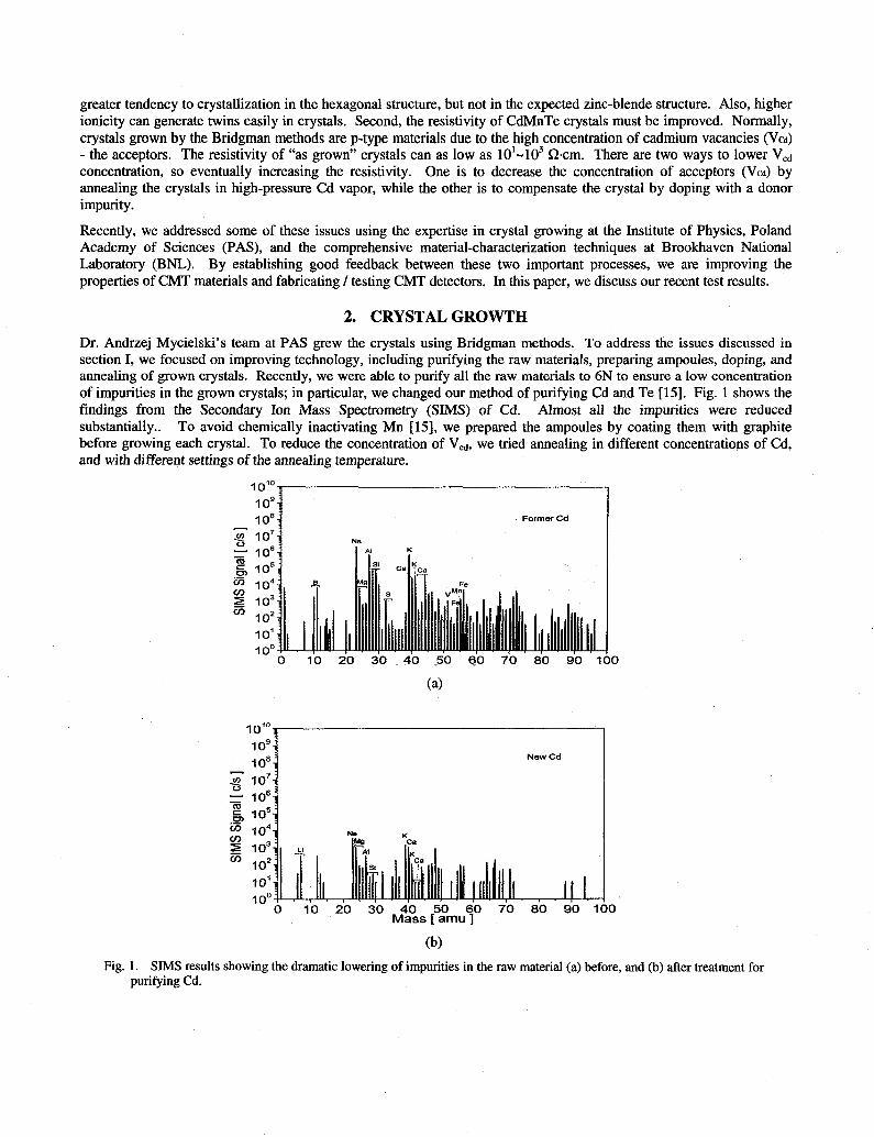
1. INTRODUCTION Cdl-,Mn,Te (CdMnTe or CMT) is a well-studied diluted magnetic semiconductor used in Faraday rotators and optical isolators, solar cells, lasers, and infrared detectors [ 13. Recently, it was proposed as potential material for gamma-ray detectors [2][5]. Burger et al. reported their findings from the first investigation of its potential for radiation-detection applications [2]. Their vanadium-doped Cd085Mn~.~~Te and Cdo.55M~.45Te had a high resistivity of 1 ~ 1 0 ' ~ n-cm, but a low mobility-lifetime product (pz) of 1 ~ 1 0 - ~ cm2N.
CMT offers several advantages over the well-studied CdZnTe (CZT), possibly making it a good replacement for the latter: this prospect is well discussed in [2][5]. Among its major benefits are good homogeneity and the need to add less (-50%) of a second metal (Mn or Zn) to reach an expected band gap.
The segregation coefficient of Mn in CdTe is nearly equal to unity in all directions, while that of Zn in CdTe has a coefficient of 1.35 [6]. This difference is reflected in the uniform concentration of Mn in CdTe, compared to the high variation of Zn concentration in CdTe. Such variability is very common in CZT crystals grown by the various widely used Bridgman methods. In contrast, this intrinsic characteristic of CMT enhances the yield of crystals suitable for use in detectors, and ultimately, might lower costs of producing large-area arrays.
X-ray diffraction experiments demonstrated that the bulk modulus increases rapidly after adding Mn to CdTe [7], while its gap energy and lattice constant vary linearly with the percentage of Mn. At room temperature, these parameters are related as described in [8] [9]
a(& = 6.482 - 0.150x, Eg(eV) = 1.526 + 1.316~
where x is the percentage of Mn added to CdTe. These equations show that adding Mn increases the room-temperature band gap at a rate of 13 meV/[%Mn], i.e., more than twice as large as the increase after adding Zn to CdTe [lo]. In fact, when x = 0.05, the energy gap of Cd0.9~Mno.05Te is about 1.60 eV that is the same as that of Cdo.gZno.lTe (the standard composition for spectrometer-grade material). Therefore, the band gap in the range 1.7-2.2 eV, which has proved ideal for assuring optimal signallnoise ratio in X-ray and gamma-ray detectors [ 1 11, can be attained by adding a relatively less (-50%) of Mn.
However, several issues about material properties remain that must be improved before CMT can be usefully employed for X-ray and gamma-ray detection. First, compared to CZT, the bond-ionicity of CMT is higher [12][13] resulting in
* [email protected]; phone 1 631 344-5351; fax 1 631 344-5773
greater tendency to crystallization in the hexagonal structure, but not in the expected zinc-blende structure. Also, higher ionicity can generate twins easily in crystals. Second, the resistivity of CdMnTe crystals must be improved. Normally, crystals grown by the Bridgman methods are p-type materials due to the high concentration of cadmium vacancies (Vcd) - the acceptors. The resistivity of “as grown” crystals can as low as 10’-103 Rem. There are two ways to lower V,, concentration, so eventually increasing the resistivity. One is to decrease the concentration of acceptors (VCd) by annealing the crystals in high-pressure Cd vapor, while the other is to compensate the crystal by doping with a donor impurity.
Recently, we addressed some of these issues using the expertise in crystal growing at the Institute of Physics, Poland Academy of Sciences (PAS), and the comprehensive material-characterization techniques at Brookhaven National Laboratory (BNL). By establishing good feedback between these two important processes, we are improving the properties of CMT materials and fabricating / testing CMT detectors. In this paper, we discuss our recent test results.
2. CRYSTAL GROWTH Dr. Andrzej Mycielski’s team at PAS grew the crystals using Bridgman methods. To address the issues discussed in section I, we focused on improving technology, including purifying the raw materials, preparing ampoules, doping, and annealing of grown crystals. Recently, we were able to purify all the raw materials to 6N to ensure a low concentration of impurities in the grown crystals; in particular, we changed our method of purifying Cd and Te [15]. Fig. 1 shows the findings from the Secondary Ion Mass Spectrometry (SIMS) of Cd. Almost all the impurities were reduced substantially.. To avoid chemically inactivating Mn [15], we prepared the ampoules by coating them with graphite before growing each crystal. To reduce the concentration of Vcd, we tried annealing in different concentrations of Cd, and with different settings of the annealing temperature.
Former Cd
- = I O 6 g 10’ 2 i o4 r io3 v, 102
I O ’ 1 oo
m
0 10 20 30 . 40 -50 60 70 80 90 I00
New Cd
I”
1 0’ 1 o8 10’ = lo6 6 i o 5
r i o3 cn I O 2
I O ’
-
3 104 v)
”‘0 10 20 30 40 50 60 70 80 90 1 Mass [ amu 1
(b)
0
Fig. 1. SIMS results showing the dramatic lowering of impurities in the raw material (a) before, and (b) after treatment for purifying Cd.
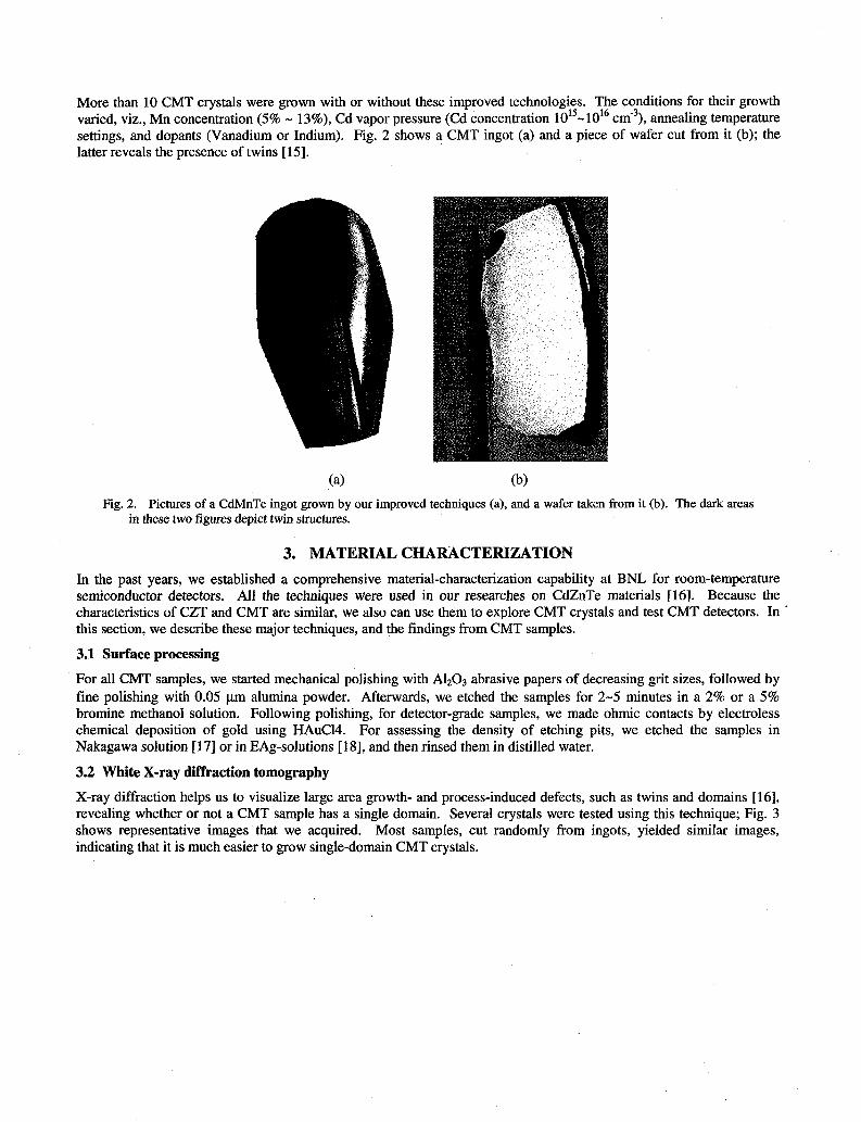
More than 10 CMT crystals were grown with or without these improved technologies. The conditions for their growth varied, viz., Mn concentration (5% - 13%), Cd vapor pressure (Cd concentration 10'5-10'6 cm-'), annealing temperature settings, and dopants (Vanadium or Indium). Fig. 2 shows a CMT ingot (a) and a piece of wafer cut from it (b); the latter reveals the presence of twins [15].
Fig. 2. Pictures of a CdMnTe ingot grown by our improved techniques (a), and a wafer taken from it (b). The dark areas in these two figures depict twin structures.
3. MATERIAL CHARACTERIZATION In the past years, we established a comprehensive material-characterization capability at BNL for room-temperature semiconductor detectors. All the techniques were used in our researches on CdZnTe materials [16]. Because the characteristics of CZT and CMT are similar, we also can use them to explore CMT crystals and test CMT detectors. In . this section, we describe these major techniques, and the findings from CMT samples.
3.1 Surface processing For all CMT samples, we started mechanical polishing with AI2O3 abrasive papers of decreasing grit sizes, followed by fine polishing with 0.05 pm alumina powder. Afterwards, we etched the samples for 2-5 minutes in a 2% or a 5% bromine methanol solution. Following polishing, for detector-grade samples, we made ohmic contacts by electroless chemical deposition of gold using HAuC14. For assessing the density of etching pits, we etched the samples in Nakagawa solution [17] or in EAg-solutions [18], and then rinsed them in distilled water.
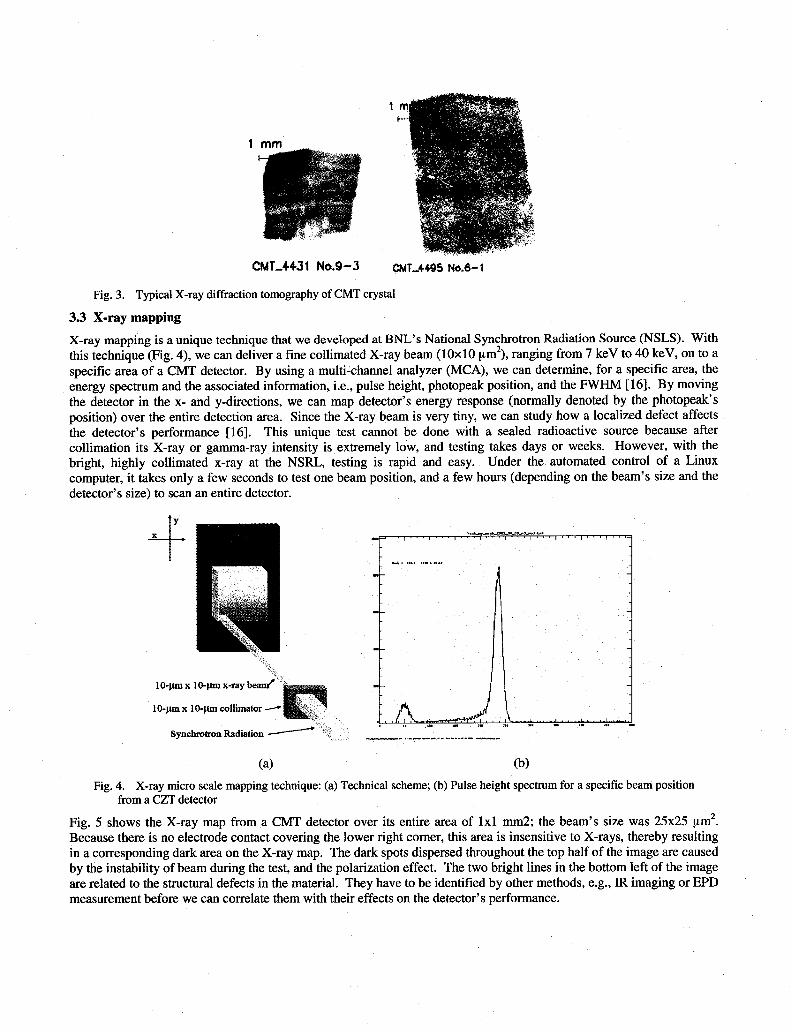
3.2 White X-ray diffraction tomography X-ray diffraction helps us to visualize large area growth- and process-induced defects, such as twins and domains [ 161, revealing whether or not a CMT sample has a single domain. Several crystals were tested using this technique; Fig. 3 shows representative images that we acquired. Most samples, cut randomly from ingots, yielded similar images, indicating that it is much easier to grow single-domain CMT crystals.
1
1
CMT-4431 NO.9-3 CMT-44.95 N0.6- 1
Fig. 3. Typical X-ray diffraction tomography of CMT crystal
3.3 X-ray mapping X-ray mapping is a unique technique that we developed at BNL’s National Synchrotron Radiation Source (NSLS). With this technique (Fig. 4), we can deliver a fine collimated X-ray beam (10x10 pm2), ranging from 7 keV to 40 keV, on to a specific area of a CMT detector. By using a multi-channel analyzer (MCA), we can determine, for a specific area, the energy spectrum and the associated information, i.e., pulse height, photopeak position, and the FWHM [16]. By moving the detector in the x- and y-directions, we can map detector’s energy response (normally denoted by the photopeak’s position) over the entire detection area. Since the X-ray beam is very tiny, we can study how a localized defect affects the detector’s performance [16]. This unique test cannot be done with a sealed radioactive source because after collimation its X-ray or gamma-ray intensity is extremely low, and testing takes days or weeks. However, with the bright, highly collimated x-ray at the NSRL, testing is rapid and easy. Under the automated control of a Linux computer, it takes only a few seconds to test one beam position, and a few hours (depending on the beam’s size and the detector’s size) to scan an entire detector.
Y..
Y * .I, 2 ..,,a 1.1.
...
10-pn x IO-pn x-ray be
IO-pn x 10-pm collimator
Synchrotron Radiation
(a) (b) Fig. 4. X-ray micro scale mapping technique: (a) Technical scheme; (b) Pulse height spectrum for a specific beam position
from a CZT detector Fig. 5 shows the X-ray map from a CMT detector over its entire area of 1x1 mm2; the beam’s size was 25x25 pm2. Because there is no electrode contact covering the lower right corner, this area is insensitive to X-rays, thereby resulting in a corresponding dark area on the X-ray map. The dark spots dispersed throughout the top half of the image are caused by the instability of beam during the test, and the polarization effect. The two bright lines in the bottom left of the image are related to the structural defects in the material. They have to be identified by other methods, e.g., IR imaging or EPD measurement before we can correlate them with their effects on the detector’s performance.
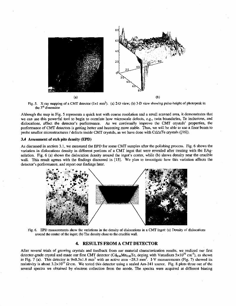
Fig. 5. X-ray mapping of a CMT detector (1x1 mm'). (a) 2-D view; (b) 3-D view showing pulse-height of photopeak in the 3rd dimension
Although the map in Fig. 5 represents a quick test with coarse resolution and a small scanned area, it demonstrates that we can use this powerful tool to begin to correlate how microscale defects, e.g., twin boundaries, Te inclusions, and dislocations, affect the detector's performance. As we continually improve the CMT crystals' properties, the performance of CMT detectors is getting better and becoming more stable. Thus, we will be able to use a finer beam to probe smaller microstructures / defects inside CMT crystals, as we have done with CdZnTe crystals ([16]).
3.4 Assessment of etch pits density (EPD) As discussed in section 3.1, we measured the EPD for some CMT samples after the polishing process. Fig. 6 shows the variation in dislocations density in different portions of a CMT ingot that were revealed after treating with the EAg- solution. Fig. 6 (a) shows the dislocation density around the ingot's center, while (b) shows density near the crucible wall. This result agrees with the findings discussed in [15]. We plan to investigate how this variation affects the detector's performance, and report our findings later.
Fig. 6. EPD measurements show the variations in the density of dislocations in a CMT ingot: (a) Density of dislocations around the center of the ingot; (b) The density close to the crucible wall.
4. RESULTS FROM A CMT DETECTOR After several trials of growing crystals and feedback from our material characterization results, we realized our first detector-grade crystal and made our first CMT detector (C&,9&ho.o6Te, doping with Vanadium 5 ~ 1 0 ' ~ cm-'), as shown in Fig. 7 (a). This detector is 9x8.5x1.8 m3 with an active area -28.3 mm2. I-V measurements (Fig. 7) showed its resistivity is about 3.2~10" R-cm. We tested this detector using a sealed Am-241 source. Fig. 8 plots three out of the several spectra we obtained by electron collection from the anode. The spectra were acquired at different biasing
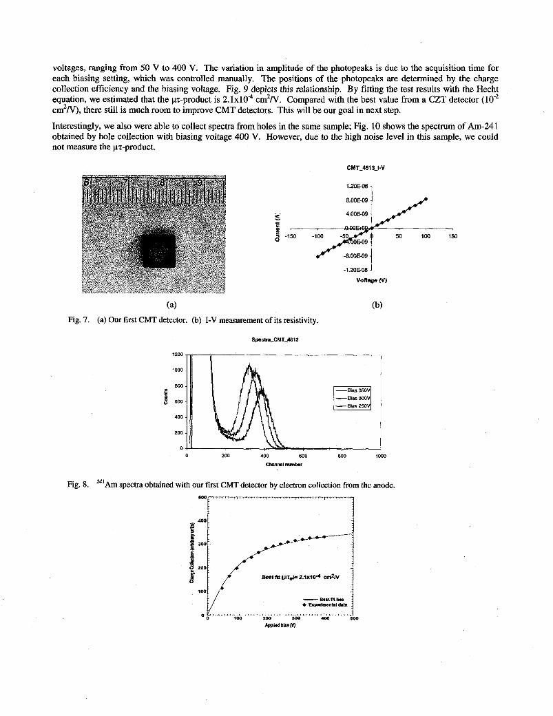
voltages, ranging from 50 V to 400 V. The variation in amplitude of the photopeaks is due to the acquisition time for each biasing setting, which was controlled manually. The positions of the photopeaks are determined by the charge collection efficiency and the biasing voltage. Fig. 9 depicts this relationship. By fitting the test results with the Hecht equation, we estimated that the pz-product is 2.1~10" cm2N. Compared with the best value from a CZT detector cm2N), there still is much room to improve CMT detectors. This will be our goal in next step.
Interestingly, we also were able to collect spectra from holes in the same sample; Fig. 10 shows the spectrum of Am-241 obtained by hole collection with biasing voltage 400 V. However, due to the high noise level in this sample, we could not measure the pz-product.
Fig. 7. (a) Our first CMT detector. (b) I-V measurement of its resistivity.
1200
1000
800
0 t 600
400
zoo
0
Spectra-CMT-4513
-Bias 300V
0
-- 200 400 600 800 1000
Channel number
Fig. 8. "'Am spectra obtained with our first CMT detector by electron collection from the anode. rrrr*jm*-n7nrr*nr---*~--,
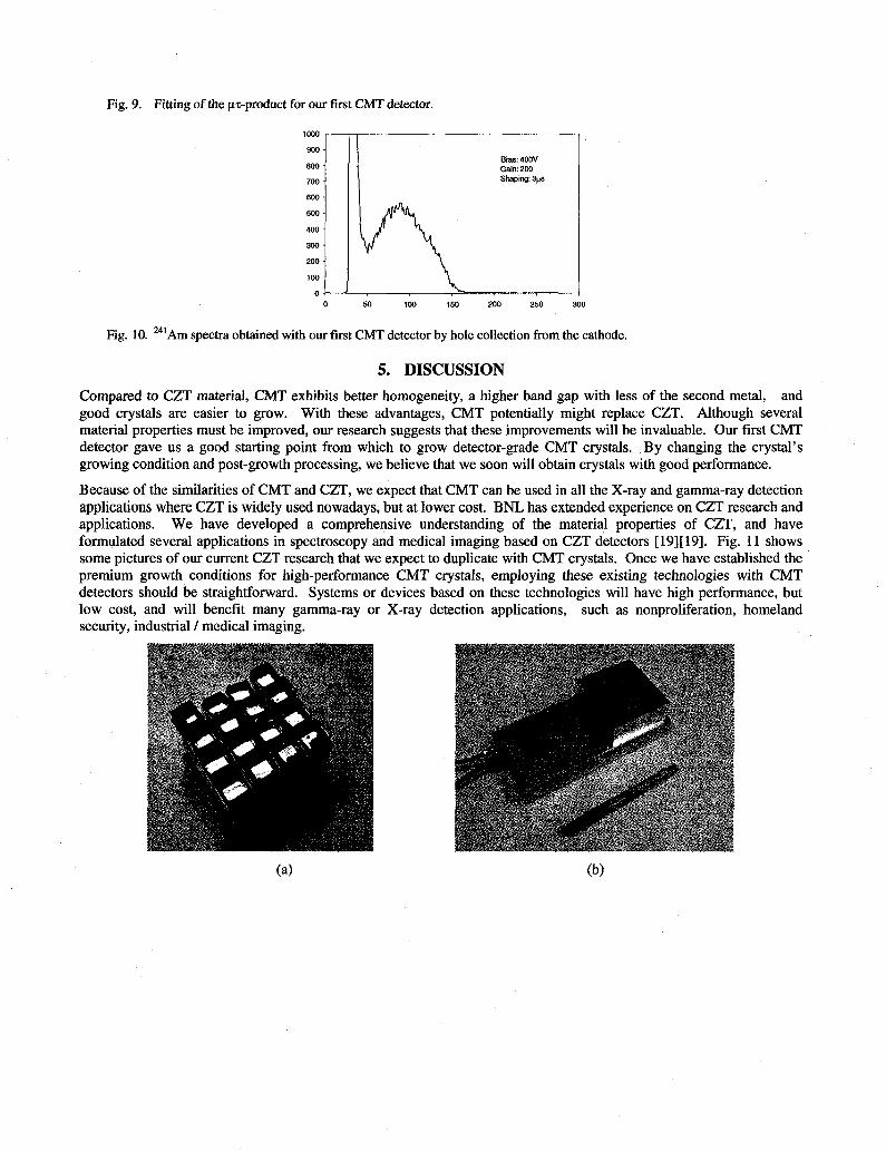
Fig. 9. Fitting of the pz-product for our first CMT detector.
1000
600
4M)
340
200 :[ 100
Bias: 400V Gain: 200 Shapiwg: 3ps
50 100 150 200 250 300
Fig. 10. %‘Am spectra obtained with our first CMT detector by hole collection from the cathode.
5. DISCUSSION Compared to CZT material, CMT exhibits better homogeneity, a higher band gap with less of the second metal, and good crystals are easier to grow. With these advantages, CMT potentially might replace CZT. Although several material properties must be improved, our research suggests that these improvements will be invaluable. Our first CMT detector gave us a good starting point from which to grow detector-grade CMT crystals. By changing the crystal’s growing condition and post-growth processing, we believe that we soon will obtain crystals with good performance.
Because of the similarities of CMT and CZT, we expect that CMT can be used in all the X-ray and gamma-ray detection applications where CZT is widely used nowadays, but at lower cost. BNL has extended experience on CZT research and applications. We have developed a comprehensive understanding of the material properties of CZT, and have formulated several applications in spectroscopy and medical imaging based on CZT detectors [ 19][ 191. Fig. 11 shows some pictures of our current CZT research that we expect to duplicate with CMT crystals. Once we have established the premium growth conditions for high-performance CMT crystals, employing these existing technologies with CMT detectors should be straightforward. Systems or devices based on these technologies will have high performance, but low cost, and will benefit many gamma-ray or X-ray detection applications, such as nonproliferation, homeland security, industrial / medical imaging.

(c) Fig. 11. Applications of CZT detectors. (a) Frisch-ring CZT detector array; (b) hand-held spectrometer based on Frisch-ring
CZT detector array; and (c) CZT pixilated detector for gamma-ray imaging.
ACKNOWLEDGMENT
The United States Government retains, and the publisher, by accepting the article for publication, acknowledges, a world-wide license to publish or reproduce the published form of this manuscript, or allow others to do so, for the United States Government purposes.
REFERENCES
Booth, N. and Smith, A. S., [Infrared Detectors], Goodwin House Publishers, New York & Boston, pp. 241-248 (1997). A. Burger, K. Chattopadhyay, H. Chen, J. 0. Ndap, X. Ma, S. Trivedi, S. W. Kutcher, R. Chen, R. D. Resemeier, “Crystal growth, fabrication and evaluation of cadmium manganese telluride gamma ray detectors”, J. Cryst. Growth, vol. 198-99, pp. 872-876 (1999). A. Mycieski, A. Burger, M. Sowinska, M. Groza, A. Szadkowski, P. Wojnar, B. Witkowska, W. Kaliszek, and P. Siffert, “Is the (Cd,Mn)Te crystal a prospective material for X-ray and y-ray detectors?’, Phys. Stat. Sol. (c) 2, No.
A. Mycielski, L. Kowalczyk, R. R. Galazka, R. Sobolewski, D. Wang, A. Burger, M. Sowinska, M. Groza, P. Siffert, A. Szadkowski, B. Witkowska, W. Kaliszek, “Applications of 11-VI semimagnetic semiconductors”, J. Alloys and Compounds, vol. 423, pp 163-168 (2006). A. Owens, and A. Peacock, “Compound semiconductor radiation detectors”, Nucl. Instr. & Meth. in Phys. Res., Vol. 531, pp 18-37 (2004). A. Tanaka, Y. Masa, S. Seto, T. Kawasaki, “Zinc and selenium co-doped CdTe substrates lattice matched to HgCdTe”, J. Crystal Growth 94, pp. 166 (1989). S. B. Quadri, E. F. Skelton, A. W. Webb, “Structural studies of Cdo.g5Zno.05Te and Cdo.g&lno.loTe under pressure”, J. Vac. Sci. Technol. A 4, pp. 1971 (1986). R. Triboulet, G. Didier, “Growth and characterization of Cdl-xMnxTe and MnTe crystals; contribution to the CdTe- MnTe pseudo-binary phase diagram determination”, J. Cryst. Growth 52, pp. 614 (1981). R. Triboulet, A. Heurtel, J. Rioux, “Twin-free (Cd, Mn)Te substrates”, J. Cryst. Growth 101, pp. 131 (1990). D. J. Olego, J. P. Faurie, S. Sivananthan, and P. M. Raccah, “Optoelectronic properties of Cdl-xZnxTe films grown by molecular beam epitaxy on GaAs substrates”, Appl. Phys. Lett. 47, 1172 (1985). J. T. Toney, T. E. Schlesinger, R. B. James, “Modeling and simulation of uniformity effects in Cdsub l-xEdsub f l e gamma-ray spectrometers”, IEEE Trans. Nucl. Sci. A 428, 14 (1999). S. Perkowitz, R. Sudharsanan, J. M. Wrbbel, B. P. Clayman, and P. Becla, “Effective charge and ionicity in Cdl- ,Mn,Te”, Phys. Rev. B38, pp. 5565 (1998) R. Triboulet, “The scope of CdTe growth for production of epitaxial substrates”, Mater. Forum 15, 30 (1991). V. Lyahovitskaya, L. Chernyak, J. Greenberg, L. Kaplan, and D. Cahen, “n- And p-type post-growth self-doping of CdTe single crystals”, J. Cryst. Growth 214/215, 1155 (2000)
5, pp 1578-1585 (2005).
[I5] A. Mycielski, M. Witkowska-Baran, D. Kochanowska, R. Jakiela, A. J. Szadkowski, Y. Cui, R. James, A. Burger, M. Groza, B. Witkowska, W. Kaliszek, E. Lusakowska, and V. Domukhovski, “(Cd,Mn)Te as a New Material for X-ray and Gamma-ray Detectors”, MRS 2007, Boston. G. S. Giuseppe, N. M. Abdul-Jabbar, S. Babalola, A. E. Bolotnikov, Y. Cui, A. Hossain, E. Jackson, H. Jackson, J. R. James, A. L. Luryi, M. Groza, A. Burger, and R. B. James, Proc. SPIE, San Diego, 2007
[I7] K. Nakagawa, K. Maeda, S. Takeuchi, “Observation of dislocations in cadmium telluride by cathode luminescence microscopy,’ Appl. Phys. Lett., 34 (1979) 574.
[Ig1 M. Inoue, I. Teramoto, and S. Takayamagi, “Etch pits and polarity in CdTe crystals”, J. Appl. Phys. 33, (1962) 2578.
[19] A. E. Bolotnikov, N. M. Abdul-Jabbar, S. Babalola, G. S. Camarda, Y. Cui, A. Hossain, E. Jackson, H. Jackson, J. R. James, A. L. Luryi, and R. B. James, “Optimization of virtual Frisch-grid CdZnTe detector designs for imaging and spectroscopy of gamma rays”, Proc. SPIE, Bellingham, WA, 2007. Y. Cui, A. Bolotnikov, G. Camarda, G. Carini, G. De Geronimo, P. O’Connor, R. James, A. Kargar, M. Harrison, and D. McGregor, “Readout System for Arrays of Frisch-ring CdZnTe Detectors”, IEEE Trans. Nucl. Sci. 54(4), pp. 849-853 (2007).
c


![X-ray emission from very high energy gamma-ray sources [Horns]](https://img.pdfslide.net/doc/110x75/55986aa61a28ab2e0b8b468a/x-ray-emission-from-very-high-energy-gamma-ray-sources-horns.jpg)