Embed Size (px)
Citation preview

CEDT, INDIAN INSTITUTE OF SCIENCE, BANGALORE, INDIA 1
Combined voltage space vector locations of a dual five-level inverter fed open-end winding IM drive (a nine-level inverter)
217 Combined Voltage Vectors
384 Triangular Sectors
15,625 Switching State Combinations
• Shaded voltage vectors generate zero common-mode voltage

CEDT, INDIAN INSTITUTE OF SCIENCE, BANGALORE, INDIA 2
Common-mode voltage of the dual five-level inverter fed open-end winding IM drive
CMA AO BO COV = V +V +V 3
CMA' A'O' B'O' C'O'V = V +V +V 3
CM CMA CMA'V = V -V
• Common-mode voltage generated by individual five-level inverters (Inverter-A or Inverter-A’)
• Common-mode voltage in the phase voltage of induction motor with the proposed dual five-level inverter fed drive
Inverter-A
Inverter-A’
CEDT, INDIAN INSTITUTE OF SCIENCE, BANGALORE, INDIA 3
Groups of common-mode voltage generated by individual five-level inverter
Group Switching state of the five-level inverter (Inv.-A or Inv.-A’)
VCM
1 222 Vdc/4
2 122, 212, 221 5Vdc/24
3 022, 112, 121, 202, 211, 220 Vdc/6
4 012, 021, 102, 111, 120, 201, 210, 22-1, 2-12, -122 Vdc/8
5 002, 011, 020, 101, 110, 12-1, 1-12, 200, 21-1, 22-2, 2-11, 2-22, -112, -121, -222
Vdc/12
6 001, 010, 02-1, 0-12, 100, 11-1, 12-2, 1-11, 1-22, 20-1, 21-2, 2-10, 2-21, -102, -111, -120, -212, -221
Vdc/24
7 000, 01-1, 02-2, 0-11, 0-22, 10-1, 11-2, 1-10, 1-21, 20-2, 2-1-1, 2-20, -101, -110, -12-1, -1-12, -202, -211, -
220
0
8 00-1, 01-2, 0-10, 0-21, 10-2, 1-1-1, 1-20, 2-1-2, 2-2-1, -100, -11-1, -12-2, -1-11, -1-22, -201, -210, -22-1, -
2-12
-Vdc/24
9 00-2, 0-1-1, 0-20, 1-1-2, 1-2-1, 2-2-2, -10-1, -11-2, -1-10, -1-21, -200, -21-1, -22-2, -2-11, -2-22,
-Vdc/12
10 0-1-2, 0-2-1, 1-2-2, -10-2, -1-1-1, -1-20, -20-1, -21-2, -2-10, -2-21
-Vdc/8
11 0-2-2, -1-1-2, -1-2-1, -20-2, -2-1-1, -2-20 -Vdc/6
12 -1-2-2, -2-1-2, -2-2-1 -5Vdc/24
13 -2-2-2 -Vdc/4

Voltage vectors and corresponding switching states resulting into zero common-mode voltage in individual five-level inverter (Inv.-A or Inv.-A’)
19 Voltage Vectors24 Triangular Sectors19 Switching States
• All the shaded switching states belong to the Group-7,which generate zero common-mode voltage at the inverter poles

Combined voltage space phasor locations resulting into zero common-mode voltage (a five-level inverter voltage space phasor structure)
• Achieved when individual five-level inverters (Inv.-A and Inv.-A’) are switched using the switching states belonging to the Group-7 only.
61 Combined Voltage Vectors
96 Triangular Sectors
361 Switching State Combinations

Number of redundant switching states available for each voltage vectors of the five-level inverter with zero common-mode voltage
61 Combined Voltage Vectors
96 Triangular Sectors
361 Switching Stats Combinations
• Achieved when individual five-level inverters (Inv.-A and Inv.-A’) are switched using the switching states belonging to the Group-7 only.

CEDT, INDIAN INSTITUTE OF SCIENCE, BANGALORE, INDIA 7
Some of the voltage vectors and their redundant switching states for five-level inverter with zero common-mode voltage
Voltage
Vector
Redundant switching state combinations(switching state of Inverter-A, switching state of Inverter-A’)
1 (000,000), (0-22,0-22), (1-21,1-21), (0-11,0-11), (1-10,1-10),(2-20,2-20), (11-2,11-2), (2-1-1,2-1-1), (-12-1,-12-1), (20-2,20-2),
(-110,-110), (-211,-211), (-101,-101), (-202,-202), (-220,-220),(-1-12,-1-12), (02-2,02-2), (01-1,01-1), (10-1,10-1)
9 (000,-101), (0-11,-1-12), (02-2,-12-1), (11-2,01-1), (10-1,000),(1-21,0-22), (1-10,0-11), (2-1-1,1-10), (20-2,10-1), (2-20,1-21),
(-110,-211), (-101,-202), (01-1,-110), (-12-1,-220)
11 (000,-202), (1-10,-1-12), (01-1,-211), (2-1-1,0-11), (02-2,-220),(11-2,-110), (20-2,000), (2-20,0-22), (10-1,-101)
28 (000,-1-12), (1-10,0-22), (01-1,-101), (2-1-1,1-21), (02-2,-110),(-12-1,-211), (11-2,000), (20-2,1-10), (-110,-202), (10-1,0-11)
95 (10-1,-202), (11-2,-211), (2-1-1,-1-12), (20-2,-101)
66 (01-1,-202), (02-2,-211), (10-1,-1-12), (11-2,-101), (20-2,0-11), (2-1-1,0-22)
174 (20-2,-202)
133 (11-2,-202), (20-2,-1-12)
98 (02-2,-202), (11-2,-1-12), (20-2,0-22)

CEDT, INDIAN INSTITUTE OF SCIENCE, BANGALORE, INDIA 8
Amplitude of maximum reference space vector possible in linear range of modulation without boost in the DC-link of the proposed inverter
SR dcmax
dc
3 3V = × V
2 2
3 = V
4
1, peak SR maxmax
dc
dc
2V = × V
32 3
= × V3 4V
=2

CEDT, INDIAN INSTITUTE OF SCIENCE, BANGALORE, INDIA 9
Generation of same maximum peak fundamental amplitude of the phase voltage equivalent to that of a conventional SVPWM
based five-level inverter
• A boost of 15% in the dc-link of the proposed drive is required to generate the maximum peak fundamental amplitude of the phase voltage equivalent to that of a conventional SVPWM based five-level inverter.

CEDT, INDIAN INSTITUTE OF SCIENCE, BANGALORE, INDIA 10
Voltage space vector locations for proposed five-level inverter with common-mode voltage elimination (with dc-link boost)
61 Combined Voltage Vectors
96 Triangular Sectors
361 Switching Stats Combinations

CEDT, INDIAN INSTITUTE OF SCIENCE, BANGALORE, INDIA 11
Switching state combination selected to generate the voltage space phasors of five-level inverter with zero CMV
61 Combined Voltage Vectors
96 Triangular Sectors
61 Switching Stats Combinations

CEDT, INDIAN INSTITUTE OF SCIENCE, BANGALORE, INDIA 12
Power scheme of the proposed five-level inverter with CME

CEDT, INDIAN INSTITUTE OF SCIENCE, BANGALORE, INDIA 13
Experimental results
Two-level operationY-axis: 1 div. = 50 V
X-axis: 1 div. = 10 ms
Pole voltage (VAO)
Pole voltage (VA’O)
Phase voltage (VA’A)
Pole voltage FFT(two-level operation)
Y-axis: Normalized amplitudeX-axis: Order of harmonic
Phase voltage FFT(two-level operation)
Y-axis: Normalized amplitudeX-axis: Order of harmonic

CEDT, INDIAN INSTITUTE OF SCIENCE, BANGALORE, INDIA 14
Experimental results (contd…)
Three-level operationY-axis: 1 div. = 40 V
X-axis: 1 div. = 10 ms
Pole voltage (VAO)
Pole voltage (VA’O)
Phase voltage (VA’A)
Pole voltage FFT(three-level operation)
Y-axis: Normalized amplitudeX-axis: Order of harmonic
Phase voltage FFT(three-level operation)
Y-axis: Normalized amplitudeX-axis: Order of harmonic

CEDT, INDIAN INSTITUTE OF SCIENCE, BANGALORE, INDIA 15
Experimental results (contd…)
Pole voltage (VAO)
Pole voltage (VA’O)
Phase voltage (VA’A)
Four-level operationY-axis: 1 div. = 70 VX-axis: 1 div. = 5 ms
Pole voltage FFT(four-level operation)
Y-axis: Normalized amplitudeX-axis: Order of harmonic
Phase voltage FFT(four-level operation)
Y-axis: Normalized amplitudeX-axis: Order of harmonic

CEDT, INDIAN INSTITUTE OF SCIENCE, BANGALORE, INDIA 16
Experimental results (contd…)
Pole voltage (VAO)
Pole voltage (VA’O)
Phase voltage (VA’A)
Five-level operationY-axis: 1 div. = 75 VX-axis: 1 div. = 5 ms
Pole voltage FFT(five-level operation)
Y-axis: Normalized amplitudeX-axis: Order of harmonic
Phase voltage FFT(five-level operation)
Y-axis: Normalized amplitudeX-axis: Order of harmonic

CEDT, INDIAN INSTITUTE OF SCIENCE, BANGALORE, INDIA 17
Experimental results (contd…)
Pole voltage (VAO)
Pole voltage (VA’O)
Phase voltage (VA’A)
Over-modulation operation
Y-axis: 1 div. = 80 VX-axis: 1 div. = 5 ms
Pole voltage FFT(over-modulation operation)Y-axis: Normalized amplitude
X-axis: Order of harmonic
Phase voltage FFT(over-modulation operation)Y-axis: Normalized amplitude
X-axis: Order of harmonic

CEDT, INDIAN INSTITUTE OF SCIENCE, BANGALORE, INDIA 18
Experimental results (contd…)
Four-level operationX-axis: 1 div. = 5 ms
Five-level operationX-axis: 1 div. = 5 ms
Phase voltage (VA’A)Y-axis: 1 div. = 50 V
Phase current Y-axis: 1 div. = 1 A
Phase voltage (VA’A)Y-axis: 1 div. = 50 V
Phase current Y-axis: 1 div. = 1 A

CEDT, Indian Institute of Science CEDT, INDIAN INSTITUTE OF SCIENCE, BANGALORE, INDIA 19
Salient features of the proposed common-mode elimination scheme for multilevel inverter fed drive
• A dual five-level inverter fed open-end winding induction motor drive with elimination of common-mode voltage in the entire operating range.
• Each five-level inverter of the proposed drive is formed by cascading two conventional two-level inverters and a conventional three-level NPC inverter. Hence, the proposed drive offers simple power-bus structure compared to the five-level NPC inverter fed drive.
• There is no alternating common-mode voltage in the inverter poles as well as at the phase windings of the induction machine.

CEDT, INDIAN INSTITUTE OF SCIENCE, BANGALORE, INDIA 20
Salient features of proposed common-mode elimination scheme for multilevel inverter fed drive (contd…)
• A common DC-link is used at both the ends of the open-end winding induction machine, for both the five-level inverters.
• The DC-link voltage requirement of proposed open-end winding IM drive is nearly half as compared to that of a single five-level inverter fed conventional IM drive.
• Hence, the voltage stress on the devices is reduced and devices with lower voltage blocking capability can be used, which makes the proposed drive scheme suitable for high power applications.

CEDT, INDIAN INSTITUTE OF SCIENCE, BANGALORE, INDIA 21
CONCLUSION
In the implemented scheme, the rotor flux position is estimated from the motor phase current ripples
During the low speed region of operation, the current ripple during the zero vector periods are used for rotor flux position estimation
During the high speed region of operation, the current ripple during the active vector periods are used for rotor flux position estimation
The scheme is implemented for a three phase motor, but the scheme can be extended to any multi phase motor and also with open-end winding structure

CEDT, INDIAN INSTITUTE OF SCIENCE, BANGALORE, INDIA 22
Linearization of the Multi-level SVPWM in Over-modulation Region
By
R. S. Kanchan, P. N. Tekwani, and K. GopakumarCentre for Electronic Design and Technology,
Indian Institute of ScienceBangalore, INDIA
CEDT, INDIAN INSTITUTE OF SCIENCE, BANGALORE, INDIA 23
Ref
eren
ce s
ign
als
and
car
rier
(wt)
vAN vBN vCN0.5
-0.5
Va0
Vb
0V
c0
Vdc
/2
Vdc
/2
Vdc/2
-Vdc
/2
-Vdc
/2
-Vdc/2
Vt
π/2 π 3 π/2 2 π
Conventional two-level Sine-Triangle PWM
( )1 *
*
AN pkdc
t
dc
vV V
V
k V
k = (peak amplitude of the sinusoidal reference) / (height of the triangular carrier signal)
Linearization of the Multi-level SVPWM in the Over-Modulation Region
• Three sinusoidal (1200 phase shifted) reference signals are compared with triangular carrier• The PWM signals are generated for three phases • The pole voltage is clamped to +ve DC link bus if Vref >Vt else to –ve DC link bus
The fundamental component in the output PWM waveform is equal to

CEDT, INDIAN INSTITUTE OF SCIENCE, BANGALORE, INDIA 24
π/2 π 3 π/2 2 π(wt)
V a0
V b0
V c0
-Vdc/2
-Vdc/2
-Vdc/2
Vdc/2
Vdc/2
Vdc/2
-Vdc/2
Vdc/2
VCNVBNVAN
Conventional Sine-Triangle PWM: Over-Modulation Range
• When ref signal is greater than carrier, the pole voltages are clamped to the DC link bus voltage• The fundamental component in output PWM waveform is not given by
• But there is reduction in the fundamental component in the output voltage
Linearization of the Multi-level SVPWM in the Over-Modulation Region
1 * dcV k V

CEDT, INDIAN INSTITUTE OF SCIENCE, BANGALORE, INDIA 25
0.5
0 wt00
1 sin( )f k t
π/2 π
Linearization of the Multi-level SVPWM in the Over-Modulation Region
• Reduction in the output fundamental is proportional to the shaded area
Conventional Sine-Triangle PWM: Over-Modulation Range

CEDT, INDIAN INSTITUTE OF SCIENCE, BANGALORE, INDIA 26
Linearization of the Multi-level SVPWM in the Over-Modulation Region
MI
k
Linear range Over-modulation
0.50
0.637
0.7854
Non-linear characteristic
• The voltage transfer characteristics i.e the ratio between the output fundamental and the reference signal amplitude is non-linear in the over-modulation region
Conventional Sine-Triangle PWM

CEDT, INDIAN INSTITUTE OF SCIENCE, BANGALORE, INDIA 27
200 400 600 800 1000 1200 1400 1600 1800
Ref
ere
nc
e s
ign
als
an
d c
arr
ier
200 400 600 800 1000 1200 1400 1600 1800
V a0
V b0
V c0
200 400 600 800 1000 1200 1400 1600 18001
(wt)
v*ANv*BN v*CN
Vdc
/2
Vdc
/2
Vdc
/2
-Vdc
/2
-Vdc
/2
-Vdc
/2
π/2 π 3 π/2 2 π
0.5
-0.5
Carrier based Space-Vector PWM (SVPWM)
Linearization of the Multi-level SVPWM in the Over-Modulation Region
1 max min / 2offsetv v v
max , ,is maximum of AN BN CNv v v v
min , ,is minimum of AN BN CNv v v v
1*
for X=A,B,C
XN XN offsetv v v
• The reference signals are added with an offset voffset1
• The resultant PWM is a Space Vector PWM
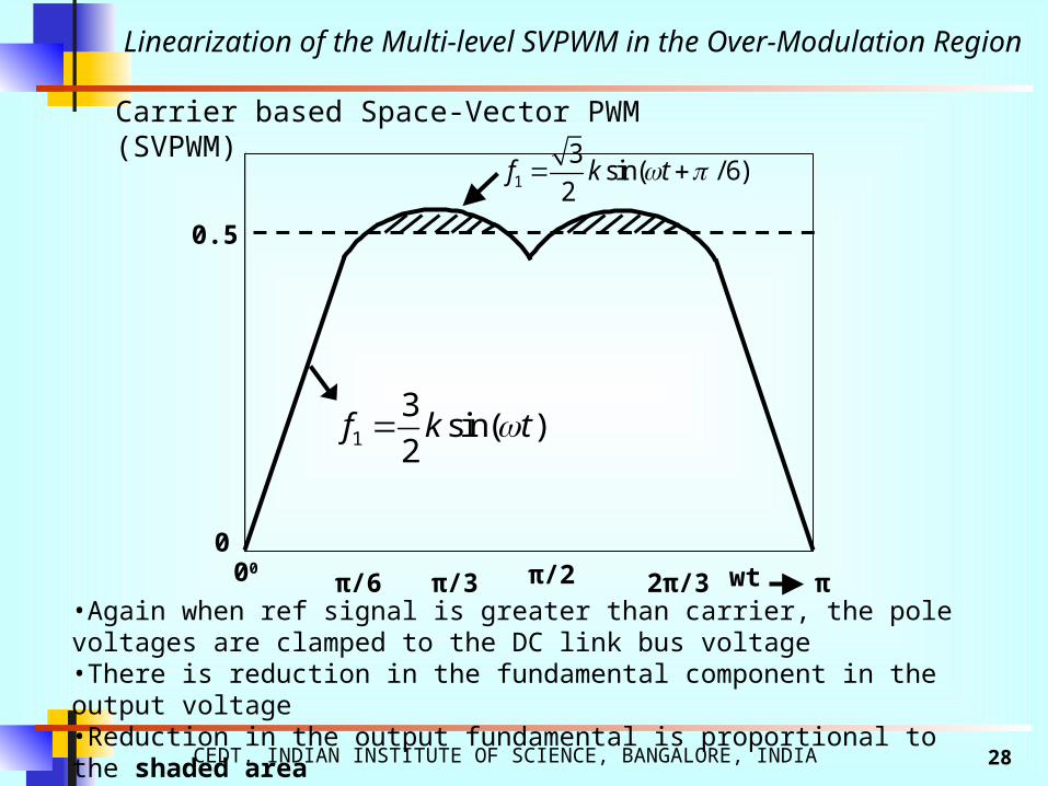
CEDT, INDIAN INSTITUTE OF SCIENCE, BANGALORE, INDIA 28
1
3sin( )
2f k t
1
3sin( / 6)
2f k t
0.5
0 wt00 π/6 π/3 π/2 2π/3 π
Linearization of the Multi-level SVPWM in the Over-Modulation Region
•Again when ref signal is greater than carrier, the pole voltages are clamped to the DC link bus voltage•There is reduction in the fundamental component in the output voltage•Reduction in the output fundamental is proportional to the shaded area
Carrier based Space-Vector PWM (SVPWM)

CEDT, INDIAN INSTITUTE OF SCIENCE, BANGALORE, INDIA 29
Linearization of the Multi-level SVPWM in the Over-Modulation Region
MI
Ou
tpu
t vo
ltag
e (p
er u
nit
w.r
.t V
dc )
Linear range Over-modulation
0.5
0.637
0.785
0.577
0.866
SPWM
SVPWM
Non-linear characteristic
• The extended linear region in SVPWM as compared to SPWM • The voltage transfer characteristics is again non-linear in the over-modulation region similar to SPWM
Ideal requirement for the PWM modulator : Linear voltage transfer characteristics

CEDT, INDIAN INSTITUTE OF SCIENCE, BANGALORE, INDIA 30
In the Proposed Work
An over-modulation scheme with the linear voltage transfer characteristics for a general n-level SVPWM signal generation
Reference signal to the PWM modulator is pre-scaled in over-modulation region such that
The fundamental component of the original and the modified reference signal is same
The modified reference signal is always within carrier region Thus voltage transfer characteristic is a linear function of the modulation index
both in the linear-modulation as well as in the over-modulation region The inverter leg switching times are directly obtained with a simple algorithm
using only the sampled amplitudes of the reference phase voltages
Linearization of the Multi-level SVPWM in the Over-Modulation Region
CEDT, INDIAN INSTITUTE OF SCIENCE, BANGALORE, INDIA 31
0 100 200 300 400 500 600 700-1
-0.5
0
0.5
1
f 1
0 100 200 300 400 500 600 700-1
-0.5
0
0.5
1
f 2 f2 fundamental
wt
k=0.637
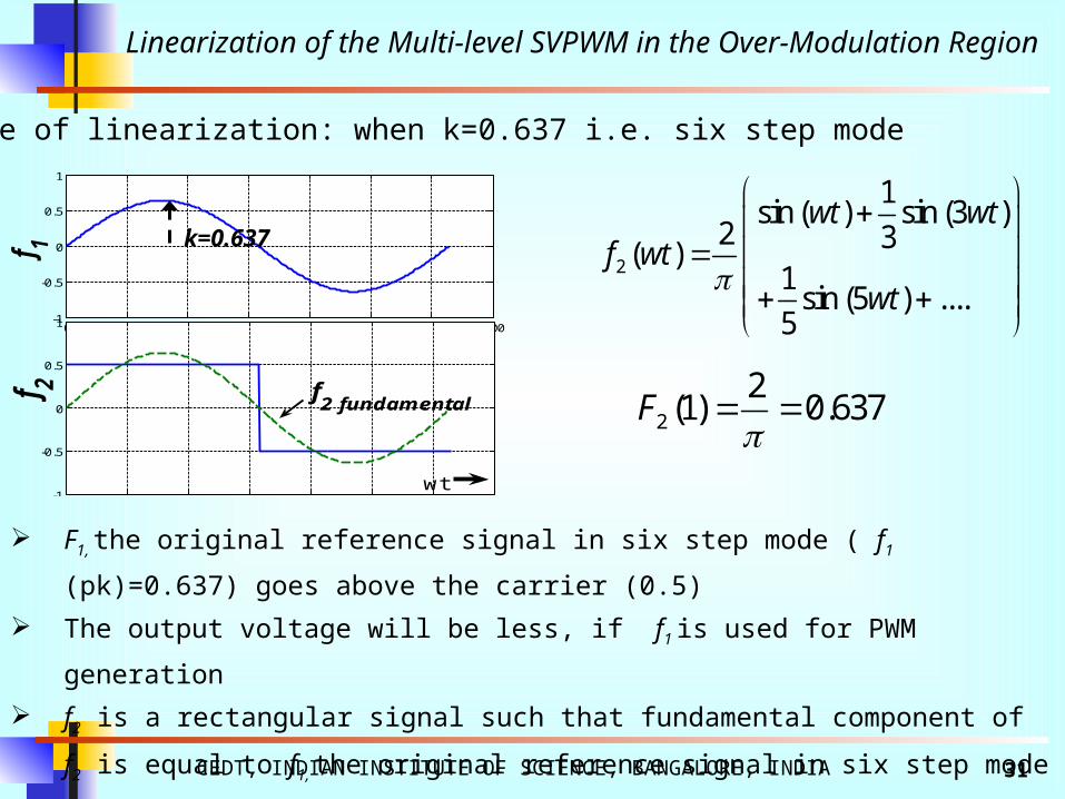
Linearization of the Multi-level SVPWM in the Over-Modulation Region
2
1sin ( ) sin (3 )
2 3( )1
sin (5 ) ....5
wt wtf wt
wt
2
2(1) 0.637F
Principle of linearization: when k=0.637 i.e. six step mode
F1, the original reference signal in six step mode ( f1 (pk)=0.637) goes above the carrier (0.5)
The output voltage will be less, if f1 is used for PWM generation
f2 is a rectangular signal such that fundamental component of f2 is equal to f1, the original
reference signal in six step mode i.e. F2 (1)=0.637
Therefore, f2 can be used for PWM generation instead of f1

CEDT, INDIAN INSTITUTE OF SCIENCE, BANGALORE, INDIA 32
θ π-θ 2π-θπ +θπ/2 π 3 π/2 2 π
-1
0
1
f 2
-0.5
0
0.5
-1
0
1
f 1
-0.5
0
0.5
mo
dif
ied
ref
.s
ign
al
Ref
eren
ces
ign
al
Linearization of the Multi-level SVPWM in the Over-Modulation
Region
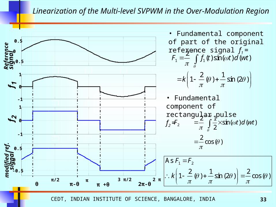
Principle of linearization: when 0.5 < k < 0.637
• A part of original reference signal is clamped• The fundamental component of the modified reference signal is same as original reference signal
• This requires that the fundamental component of rectangular pulse f2 is equal to fundamental component of part of the original reference signal f1
CEDT, INDIAN INSTITUTE OF SCIENCE, BANGALORE, INDIA 33
θ π-θ 2π-θπ +θπ/2 π 3 π/2 2 π
-1
0
1
f 2
-0.5
0
0.5
-1
0
1
f 1
-0.5
0
0.5
mo
dif
ied
re
f.si
gn
al
R
efe
ren
ce
sig
na
l
Linearization of the Multi-level SVPWM in the Over-Modulation
Region
1 1
2( )sin( ) ( )
2 11 ( ) sin (2 )
F f t t d wt
k
2
2 1sin( ) ( )
2
2cos ( )
F t d wt
1 2As
2 1 21 ( ) sin (2 ) cos ( )
F F
k
• Fundamental component of rectangular pulse f2 =
• Fundamental component of part of the original reference signal f1 =

CEDT, INDIAN INSTITUTE OF SCIENCE, BANGALORE, INDIA 34
0 10 20 30 40 50 60 70 80 900.7854
0.8168
0.8482
0.8796
0.9111
0.9524
0.9739
1
MI
Linearization of the Multi-level SVPWM in the Over-Modulation Region
2 1 21 ( ) sin (2 ) cos ( )k
/ 0.637MI k
• The relationship between modulation index MI and clamping angle
• Thus if MI is known, the clamping angle can be determined• The modified reference signal is clamped for the angle to π-θ and π+θ to 2π-θ

CEDT, INDIAN INSTITUTE OF SCIENCE, BANGALORE, INDIA 35
0.5
0
wt00
1
3sin( )
2f k t
1
3sin( / 6)
2f k t k
π/6 π/3 π/2 2π/3π
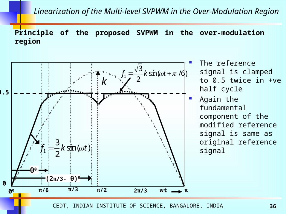
Principle of the proposed SVPWM in the over-modulation region
Linearization of the Multi-level SVPWM in the Over-Modulation Region
1
3( ) sin( ); 0
2 6
3sin( );
2 6 6 2
f t k t t
k t t
Reference signal goes out of the carrier two times in the positive half cycle
Modified reference signal
CEDT, INDIAN INSTITUTE OF SCIENCE, BANGALORE, INDIA 36
0.5
0 wt
θ0
00
1
3sin( )
2f k t
1
3sin( / 6)
2f k t
k
π/6 π/3 π/2
(2π/3- θ)0
2π/3 π
Linearization of the Multi-level SVPWM in the Over-Modulation Region
Principle of the proposed SVPWM in the over-modulation region
The reference signal is clamped to 0.5 twice in +ve half cycle
Again the fundamental component of the modified reference signal is same as original reference signal
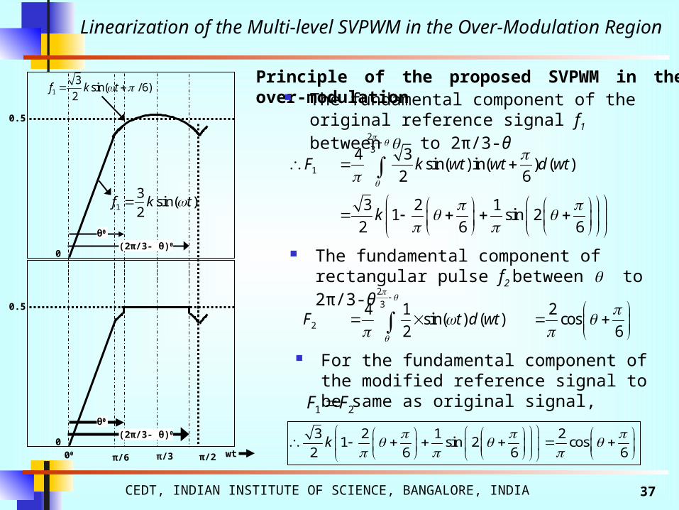
CEDT, INDIAN INSTITUTE OF SCIENCE, BANGALORE, INDIA 37
0.5
0 wt
θ0
00 π/6 π/3 π/2
(2π/3- θ)0
2
3
1
4 3sin( ) in( ) ( )
2 6
3 2 11 sin 2
2 6 6
F k wt wt d wt
k
2
3
2
4 1 2sin( ) ( ) cos
2 6F t d wt
3 2 1 21 sin 2 cos
2 6 6 6k
Principle of the proposed SVPWM in the over-modulation
Linearization of the Multi-level SVPWM in the Over-Modulation Region
The fundamental component of the original reference signal f1 between to 2π/3-θ0.5
0
θ0
1
3sin( )
2f k t
1
3sin( / 6)
2f k t
(2π/3- θ)0
The fundamental component of rectangular pulse f2 between to 2π/3-θ
For the fundamental component of the modified reference signal to be same as original signal,
1 2F F
CEDT, INDIAN INSTITUTE OF SCIENCE, BANGALORE, INDIA 38
0.5
0 wt
θ0
00
1
3sin( )
2f k t
1
3sin( / 6)
2f k t
π/6 π/3 π/2
(2π/3- θ)0
3 2 1 21 sin 2 cos
2 6 6 6k
Linearization of the Multi-level SVPWM in the Over-Modulation Region
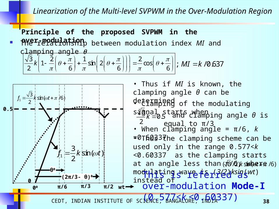
The relationship between modulation index MI and clamping angle
Principle of the proposed SVPWM in the over-modulation
• Thus if MI is known, the clamping angle θ can be determined
; / 0.637MI k
• Clamping of the modulating signal starts when3
0.52
k and clamping angle θ is equal to π/3
• When clamping angle = π/6, k =0.60337• Thus the clamping scheme can be used only in the range 0.577<k <0.60337 as the clamping starts at an angle less than π/6, where modulating wave is (3/2)ksin(wt) instead of
This is referred as over-modulation Mode-I (0.577<k <0.60337)
( 3 / 2) sin( / 6)k t

CEDT, INDIAN INSTITUTE OF SCIENCE, BANGALORE, INDIA 39
0.5
0 wt
θ0
(π -θ)0
00
1
3sin( )
2f k t
1
3sin( / 6)
2f k t
k
π/6 π/3 π/2 2π/3π
.
• The MI range greater than 0.60337, angle θ at which clamping starts is less than π/3
Linearization of the Multi-level SVPWM in the Over-Modulation Region
Principle of the proposed SVPWM in the over-modulation MODE-II The reference signal is clamped to 0.5 for θ < wt < π- θ Again the fundamental component of the modified reference signal is same
as original reference signal (dotted line)

CEDT, INDIAN INSTITUTE OF SCIENCE, BANGALORE, INDIA 40
• The relationship between θ and k can be derived similarly
Linearization of the Multi-level SVPWM in the Over-Modulation Region
Principle of the proposed SVPWM in the over-modulation MODE-II
3 31 ( ) sin (2 )
2
2cos ( )
k
0.5
0 wt
θ0
(π -θ)0
00
1
3sin( )
2f k t
1
3sin( / 6)
2f k t
k
π/6 π/3 π/2 2π/3 π
.
5π/6

CEDT, INDIAN INSTITUTE OF SCIENCE, BANGALORE, INDIA 41
Linearization of the Multi-level SVPWM in the Over-Modulation Region
• Over-modulation Mode-II (0.60337<k <0.637) & clamping angle 0<θ< π/3
• Over-modulation Mode-I (0.577<k <0.60337) & clamping angle π/3<θ< π/6
3 3 21 ( ) sin (2 ) cos ( )
2k
3 2 1 21 sin 2 cos
2 6 6 6k
Summary: The relationship between θ and k
Principle of the proposed SVPWM in the over-modulation MODE-II

CEDT, INDIAN INSTITUTE OF SCIENCE, BANGALORE, INDIA 42
Linearization of the Multi-level SVPWM in the Over-Modulation Region
0 10 20 30 40 50 60 70 80 900.7854
0.8168
0.8482
0.8796
0.9111
0.9524
0.9739
1
MI
0 10 20 30 40 50 60 70 80 900.5
0.52
0.54
0.56
0.58
0.6
0.62
0.64
k
SVPWM
SPWM
Mode-IMode-II
The relationship between θ and k (MI) for SPWM and SVPWM
Steps• Read Modulation Index MI• Determine clamping angle θ• Clamp the reference signal to 0.5 appropriately• The implementation needs instantaneous angle information

CEDT, INDIAN INSTITUTE OF SCIENCE, BANGALORE, INDIA 43
Modified reference voltages and triangular carriers for a five-level SVPWM scheme
1 max min / 2offsetv v v
1*
for X=A,B,C
XN XN offsetv v v
• n-level SPWM scheme uses n-1 level shifted carrier waves• Sinusoidal reference signals are added with offset which centers them within carrier region
max , ,is maximum of AN BN CNv v v v
min , ,is minimum of AN BN CNv v v v
Space Vector PWM signal generation for multi-level inverters using only the sampled amplitudes of reference phase voltages
CEDT, INDIAN INSTITUTE OF SCIENCE, BANGALORE, INDIA 44
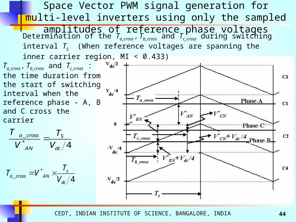
Determination of the Ta_cross , Tb_cross and Tc_cross during switching interval TS (When
reference voltages are spanning the inner carrier region, MI < 0.433)
Ta_cross , Tb_cross and Tc_cross : the time duration from the start of switching interval when the reference phase - A, B and C cross the carrier
Space Vector PWM signal generation for multi-level inverters using only the sampled amplitudes of reference phase voltages
_
* 4a cross S
AN dc
T T
V V
*_ 4
sa cross AN
dc
TT V
V

CEDT, INDIAN INSTITUTE OF SCIENCE, BANGALORE, INDIA 45
*1
* *_
* *_
* *_
for X=A,B,C
4
( 4)4
( 4)4
XN XN offset
sa cross AN as
dc
sb cross BN dc bs s
dc
sc cross CN dc cs s
dc
V V V
TT V T
V
TT V V T T
V
TT V V T T
V
Determination of the Ta_cross , Tb_cross and Tc_cross during switching interval TS (When
reference voltages are spanning the inner carrier region, MI < 0.433)
T*as , T*
bs and T*cs : Time equivalents of the modified reference signal amplitudes
Carrier- C1
Carrier- C2
Carrier- C2
* * * *
* * * *1 1
,4 4
,4 4
S Sas AN bs BN
dc dc
S Scs CN offset offset
dc dc
T TT V T V
V V
T TT V T V
V V
Space Vector PWM signal generation for multi-level inverters using only the sampled amplitudes of reference phase voltages

CEDT, INDIAN INSTITUTE OF SCIENCE, BANGALORE, INDIA 46
Determination of the Ta_cross , Tb_cross and Tc_cross during switching interval TS (When
reference voltages are spanning the entire carrier region, 0.433<MI < 0.866)
*_
*
*_
*
*_
*
( 4)4
( 2)4
2
( 4)4
Sa cross AN dc
dc
as S
Sb cross BN dc
dc
bs S
Sc cross CN dc
dc
cs S
TT V V
V
T T
TT V V
V
T T
TT V V
V
T T
Space Vector PWM signal generation for multi-level inverters using only the sampled amplitudes of reference phase voltages

CEDT, INDIAN INSTITUTE OF SCIENCE, BANGALORE, INDIA 47
SUMMARY: Ta_cross , Tb_cross and Tc_cross for various carrier regions to bring the reference within a carrier region
* *
4S
xs XNdc
TT V
V
*
* 4xs S
XN dc
T T
V V
: 4S dcT V
Space Vector PWM signal generation for multi-level inverters using only the sampled amplitudes of reference phase voltages
CEDT, INDIAN INSTITUTE OF SCIENCE, BANGALORE, INDIA 48
*
* 4as S
AN dc
T T
V V
3600
1800900 270000 wt
ST
2* ST
2* ST
ST
*asT
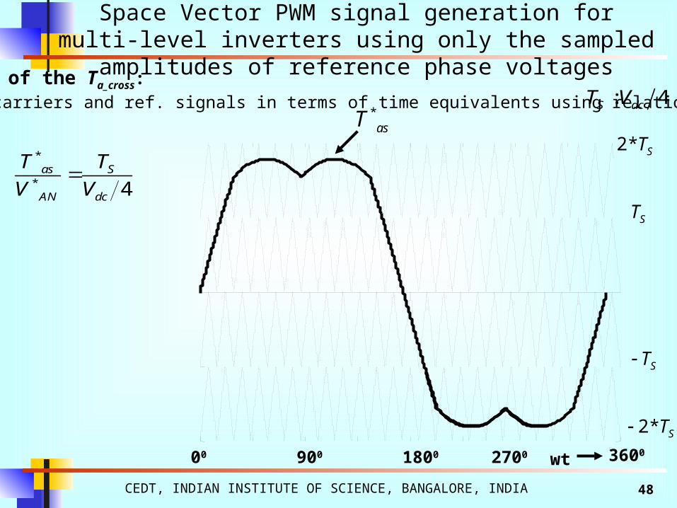
: 4S dcT VDetermination of the Ta_cross:
Represent the carriers and ref. signals in terms of time equivalents using relationship
Space Vector PWM signal generation for multi-level inverters using only the sampled amplitudes of reference phase voltages

CEDT, INDIAN INSTITUTE OF SCIENCE, BANGALORE, INDIA 49
*
* 4as S
AN dc
T T
V V
: 4S dcT V
36001800900 270000 wt
ST
2* ST
2* ST
ST
*_a cross as ST T T
Space Vector PWM signal generation for multi-level inverters using only the sampled amplitudes of reference phase voltages
Determination of the Ta_cross:
Shift the ref. signal into one carrier region (first +ve carrier) by adding proper offset

CEDT, INDIAN INSTITUTE OF SCIENCE, BANGALORE, INDIA 50
*
* 4as S
AN dc
T T
V V
: 4S dcT V
36001800900 270000 wt
ST
2* ST
2* ST
ST
*_a cross as ST T T
Space Vector PWM signal generation for multi-level inverters using only the sampled amplitudes of reference phase voltages
Determination of the Ta_cross

CEDT, INDIAN INSTITUTE OF SCIENCE, BANGALORE, INDIA 51
_a crossT
*
* 4as S
AN dc
T T
V V
: 4S dcT V
36001800900 270000 wt
ST
2* ST
2* ST
ST
*_ 2a cross as ST T T
Space Vector PWM signal generation for multi-level inverters using only the sampled amplitudes of reference phase voltages
Determination of the Ta_cross

CEDT, INDIAN INSTITUTE OF SCIENCE, BANGALORE, INDIA 52
Space Vector PWM signal generation for multi-level inverters using only the sampled amplitudes of reference phase voltages
Equivalence to Conventional SVPWM
• The reference signals in carrier based SVPWM are shifted to one carrier region • The outer sub-hexagon in the conventional SVPWM are shifted to central sub-hexagon in conventional SVPWM• The reference signal shifting in carrier based SVPWM is equivalent to sub-hexagonal shifting in the conventional SVPWM
180090000
*asT
180090000
_a crossT

CEDT, INDIAN INSTITUTE OF SCIENCE, BANGALORE, INDIA 53
_ _min ( )first cross x crossT T
sec _ _( )ond cross x crossT mid T_ _max ( )third cross x crossT T
_ _middle third cross first crossT T T
0 s middleT T T
0 _ 2
2 0 _
/ 2
/ 2
first cross offset
offset first cross
T T T
T T T
_ 2 for x=a,b,cgx x cross offsetT T T Inverter leg
switching times
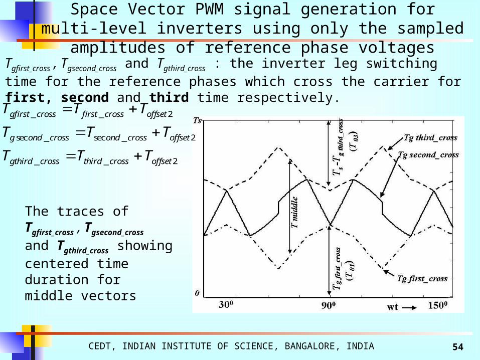
Algorithm for inverter leg switching time calculation: Tfirst_cross , Tsecond_cross and Tthird_cross : the time duration from the start of switching interval when the reference phases cross the carrier for first, second and third time respectively.
, x= a, b, c
Space Vector PWM signal generation for multi-level inverters using only the sampled amplitudes of reference phase voltages
CEDT, INDIAN INSTITUTE OF SCIENCE, BANGALORE, INDIA 54
The traces of Tgfirst_cross , Tgsecond_cross and Tgthird_cross showing centered time duration for middle vectors
Tgfirst_cross , Tgsecond_cross and Tgthird_cross : the inverter leg switching time for the reference phases which cross the carrier for first, second and third time respectively.
_ _ 2
sec _ sec _ 2
_ _ 2
gfirst cross first cross offset
g ond cross ond cross offset
gthird cross third cross offset
T T T
T T T
T T T
Space Vector PWM signal generation for multi-level inverters using only the sampled amplitudes of reference phase voltages

CEDT, INDIAN INSTITUTE OF SCIENCE, BANGALORE, INDIA 55
Space Vector PWM signal generation for multi-level inverters using only the sampled amplitudes of reference phase voltages

CEDT, INDIAN INSTITUTE OF SCIENCE, BANGALORE, INDIA 56
InverterGating SignalsTime
EquivalentsTxs
VAN
VBN
VCN
Toffset1
PWM Compa-rators
Gating Signals
Tgx
Ta_cross,
Tb_cross
Tc_cross
Toffset2
++
Schematic representation of the Multi-level SVPWM
Space Vector PWM signal generation for multi-level inverters using only the sampled amplitudes of reference phase voltages

CEDT, INDIAN INSTITUTE OF SCIENCE, BANGALORE, INDIA 57
InverterGating SignalsPre-
scaler
TimeEquivalents
Txs
VAN
VBN
VCN
MI
Toffset1
Vs
PWM Compa-rators
Gating Signals
Tgx
Ta_cross,
Tb_cross
Tc_cross
Toffset2
+
+
Implementation of the Multi-level SVPWM with Linear Transfer Characteristics in Over-Modulation
In overmodulation, clamps the reference signals appropriately
CEDT, INDIAN INSTITUTE OF SCIENCE, BANGALORE, INDIA 58
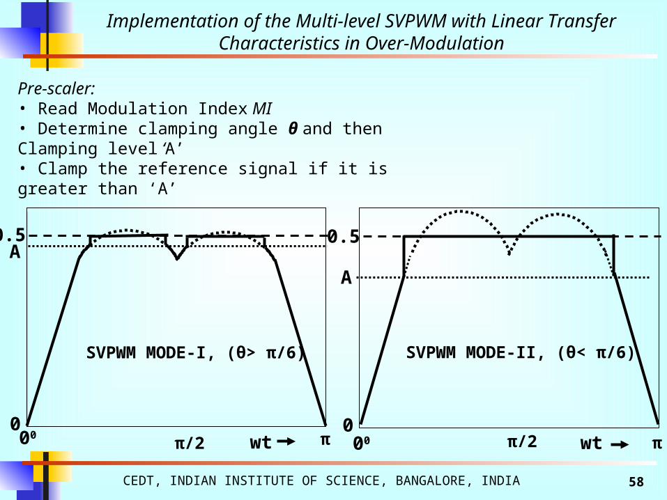
0.5
0 wt00 π/2 π
A
SVPWM MODE-I, (θ> π/6)
0.5
0 wt00 π/2 π
A
SVPWM MODE-II, (θ< π/6)
Implementation of the Multi-level SVPWM with Linear Transfer Characteristics in Over-Modulation
Pre-scaler: • Read Modulation Index MI• Determine clamping angle θ and then Clamping level ‘A’ • Clamp the reference signal if it is greater than ‘A’

CEDT, INDIAN INSTITUTE OF SCIENCE, BANGALORE, INDIA 59
0
10
20
30
40
50
60
0.9 0.92 0.94 0.96 0.98 10
0.1
0.2
0.3
0.4
0.5
Modulation Index 'MI'
Cla
mp
ing
le
ve
l 'A
'
θ
A
Linearization of the Multi-level SVPWM in the Over-Modulation Region
A for3S2
k sin / 6 * ( n 1)T / 2 / 6 / 3
A forS2
3 k sin * ( n 1)T / 2 0 / 6
The clamping angle information is converted into a level signal ‘A’
Prescaler: A simple look-up table of MI vs A

CEDT, INDIAN INSTITUTE OF SCIENCE, BANGALORE, INDIA 60
(wt)
Simulation Results: Linear-Modulation Region
Pre-scaler
TimeEquivalents
Txs
VAN
VBN
VCN
MI
Toffset1
Vs
PWM Compa-rators
Gating Signals
Tgx
Ta_cross,
Tb_cross
Tc_cross
Toffset2
++
No clamping of Tas in linear range of modulation
Pre-scaler is inactive in linear modulation range

CEDT, INDIAN INSTITUTE OF SCIENCE, BANGALORE, INDIA 61
0 0.5 1 1.5 2 2.5 3
-0.8
-0.4
0
0.4
0.8
x 10-3
0 0.5 1 1.5 2 2.5 30
2
4x 10
-4
0 0.5 1 1.5 2 2.5 30
2
4x 10
-4
0 0.5 1 1.5 2 2.5 3
-0.8
-0.4
0
0.4
0.8
x 10-3
Tas
T*as
Ta_cross
Tga
(wt)
Simulation Results: Over-Modulation Region (MI: 0.92)
Clamping of Tas in over-modulation (Mode-I)
Pre-scaler is active in over-modulation range

CEDT, INDIAN INSTITUTE OF SCIENCE, BANGALORE, INDIA 62
0 0.5 1 1.5 2 2.5 3
-0.8
-0.4
0
0.4
0.8
x 10-3
0 0.5 1 1.5 2 2.5 30
2
4x 10
-4
0 0.5 1 1.5 2 2.5 30
2
4x 10
-4
0 0.5 1 1.5 2 2.5 3
-0.8
-0.4
0
0.4
0.8
x 10-3
Tas
T*as
Ta_cross
Tga
(wt)
Simulation Results: Over-Modulation Region (MI: 0.94)
CEDT, INDIAN INSTITUTE OF SCIENCE, BANGALORE, INDIA 63
0 0.5 1 1.5 2 2.5 3
-0.8
-0.4
0
0.4
0.8
x 10-3
0 0.5 1 1.5 2 2.5 30
2
4x 10
-4
0 0.5 1 1.5 2 2.5 30
2
4x 10
-4
0 0.5 1 1.5 2 2.5 3
-0.8
-0.4
0
0.4
0.8
x 10-3
Tas
T*as
Ta_cross
Tga
(wt)
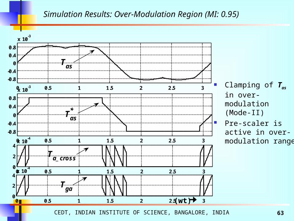
Simulation Results: Over-Modulation Region (MI: 0.95)
Clamping of Tas in over-modulation (Mode-II)
Pre-scaler is active in over-modulation range

CEDT, INDIAN INSTITUTE OF SCIENCE, BANGALORE, INDIA 64
0 0.5 1 1.5 2 2.5 3
-0.8
-0.4
0
0.4
0.8
x 10-3
0 0.5 1 1.5 2 2.5 30
2
4x 10
-4
0 0.5 1 1.5 2 2.5 30
2
4x 10
-4
0 0.5 1 1.5 2 2.5 3
-0.8
-0.4
0
0.4
0.8
x 10-3
Tas
T*as
Ta_cross
Tga
(wt)
Simulation Results: Over-Modulation Region (MI: 0.96)

CEDT, INDIAN INSTITUTE OF SCIENCE, BANGALORE, INDIA 65
0 0.5 1 1.5 2 2.5 3
-0.8
-0.4
0
0.4
0.8
x 10-3
0 0.5 1 1.5 2 2.5 30
2
4x 10
-4
0 0.5 1 1.5 2 2.5 30
2
4x 10
-4
0 0.5 1 1.5 2 2.5 3
-0.8
-0.4
0
0.4
0.8
x 10-3
Tas
T*as
Ta_cross
Tga
(wt)
Simulation Results: Over-Modulation Region (MI: 0.98 )

CEDT, INDIAN INSTITUTE OF SCIENCE, BANGALORE, INDIA 66
0 0.5 1 1.5 2 2.5 3
-0.8
-0.4
0
0.4
0.8
x 10-3
0 0.5 1 1.5 2 2.5 30
2
4x 10
-4
0 0.5 1 1.5 2 2.5 30
2
4x 10
-4
0 0.5 1 1.5 2 2.5 3
-0.8
-0.4
0
0.4
0.8
x 10-3
Tas
T*as
Ta_cross
Tga
(wt)
Simulation Results: Over-Modulation Region (MI: 1.00)
Square-wave switching mode
CEDT, INDIAN INSTITUTE OF SCIENCE, BANGALORE, INDIA 67
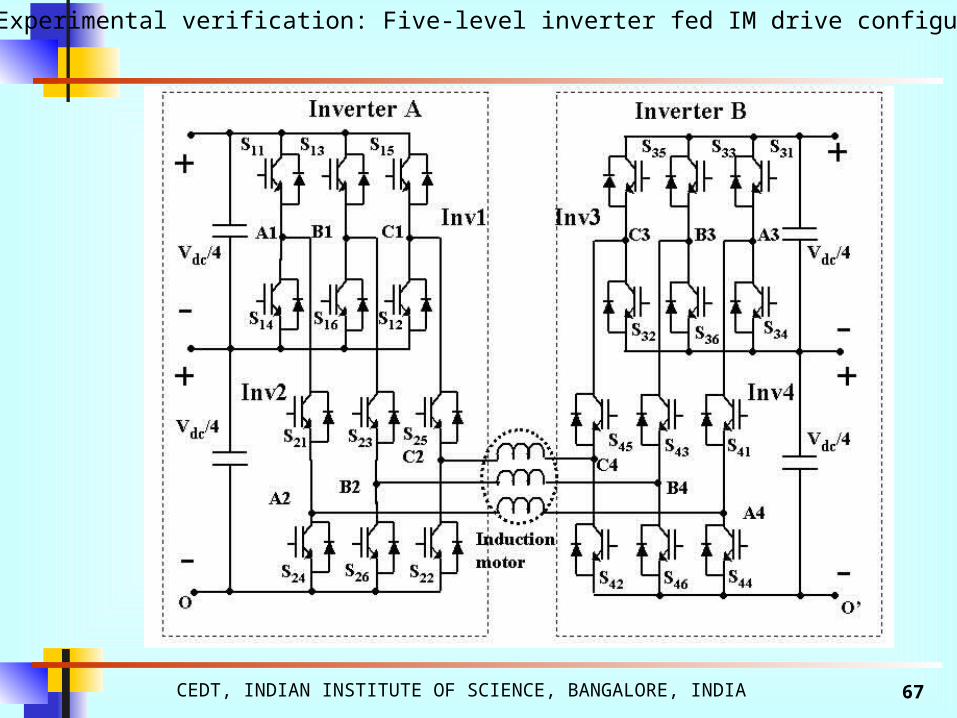
Experimental verification: Five-level inverter fed IM drive configuration

CEDT, INDIAN INSTITUTE OF SCIENCE, BANGALORE, INDIA 68
Ref: V. T. Somasekhar, K. Gopakumar, “Three - level inverter configuration cascading two 2-level inverters”, IEE Proc. – EPA, Vol. 150, No. 3, May 2003, pp.245-254
+
1C
2C
2dcV
2dcV
Inv1
Inv2
-
• Each three-level inverter configuration by cascading two two-level inverters
• The pole voltage can attain three levels:Vdc/2, 0 ,
-Vdc/2
Inverter-A
Five-level inverter fed IM drive configuration
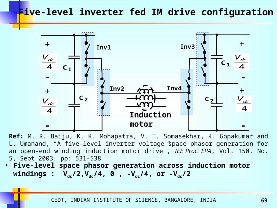
CEDT, INDIAN INSTITUTE OF SCIENCE, BANGALORE, INDIA 69
• Five-level space phasor generation across induction motor windings : Vdc/2,Vdc/4, 0 , -Vdc/4, or -Vdc/2
+
1C
2C
4dcV
4dcV
Inv1
Inv2
-
1C
2C
4dcV
4dcV
+Inv3
Inv4
-Inductionmotor
+ +
- -
Ref: M. R. Baiju, K. K. Mohapatra, V. T. Somasekhar, K. Gopakumar and L. Umanand, “A five-level inverter voltage space phasor generation for an open-end winding induction motor drive”, IEE Proc. EPA, Vol. 150, No. 5, Sept 2003, pp: 531-538
Five-level inverter fed IM drive configuration
CEDT, INDIAN INSTITUTE OF SCIENCE, BANGALORE, INDIA 70
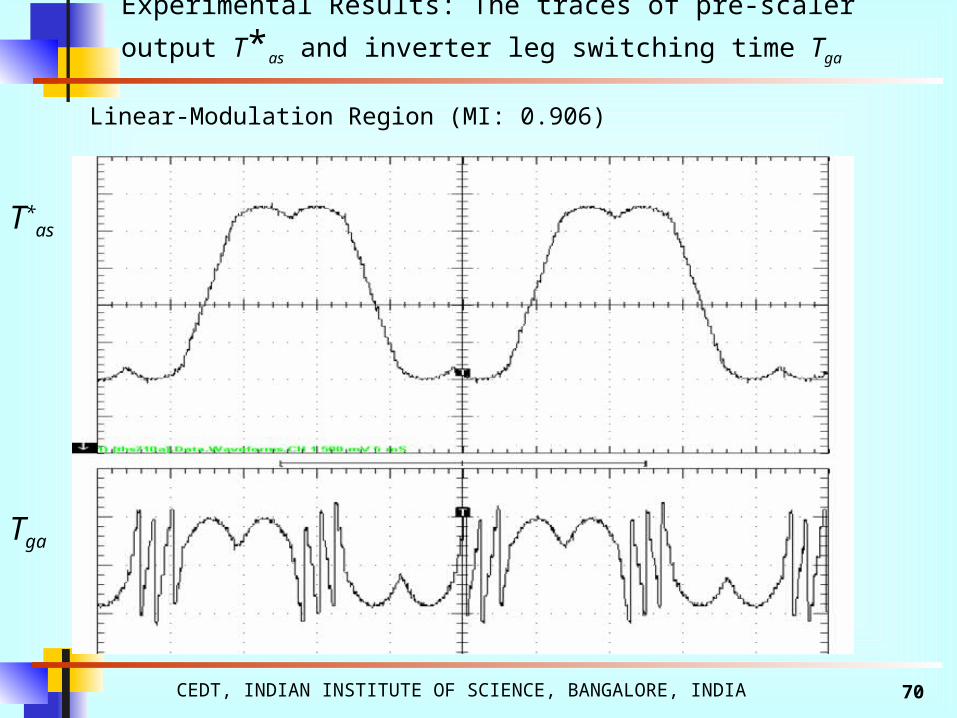
Linear-Modulation Region (MI: 0.906)
T*as
Tga
Experimental Results: The traces of pre-scaler output T*as and inverter leg switching time Tga

CEDT, INDIAN INSTITUTE OF SCIENCE, BANGALORE, INDIA 71
T*as
Tga
Over-Modulation Region (MI: 0.92)
Experimental Results: The traces of pre-scaler output T*as and inverter leg switching time Tga
CEDT, INDIAN INSTITUTE OF SCIENCE, BANGALORE, INDIA 72
T*as
Tga
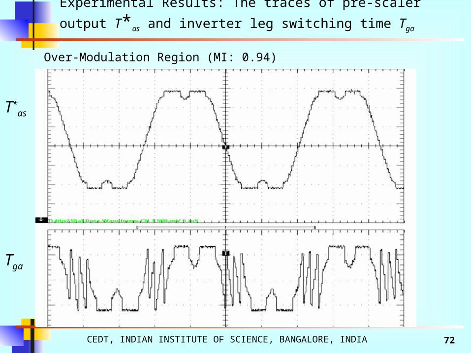
Over-Modulation Region (MI: 0.94)
Experimental Results: The traces of pre-scaler output T*as and inverter leg switching time Tga

CEDT, INDIAN INSTITUTE OF SCIENCE, BANGALORE, INDIA 73
T*as
Tga
Over-Modulation Region (MI: 0.96)
Experimental Results: The traces of pre-scaler output T*as and inverter leg switching time Tga
CEDT, INDIAN INSTITUTE OF SCIENCE, BANGALORE, INDIA 74
T*as
Tga
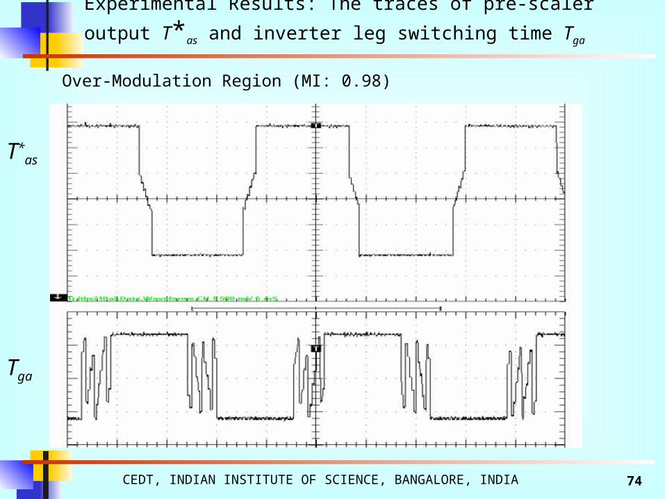
Over-Modulation Region (MI: 0.98)
Experimental Results: The traces of pre-scaler output T*as and inverter leg switching time Tga

CEDT, INDIAN INSTITUTE OF SCIENCE, BANGALORE, INDIA 75
T*as
Tga
Square wave switching mode (MI: 1.00)
Experimental Results: The traces of pre-scaler output T*as and inverter leg switching time Tga
CEDT, INDIAN INSTITUTE OF SCIENCE, BANGALORE, INDIA 76
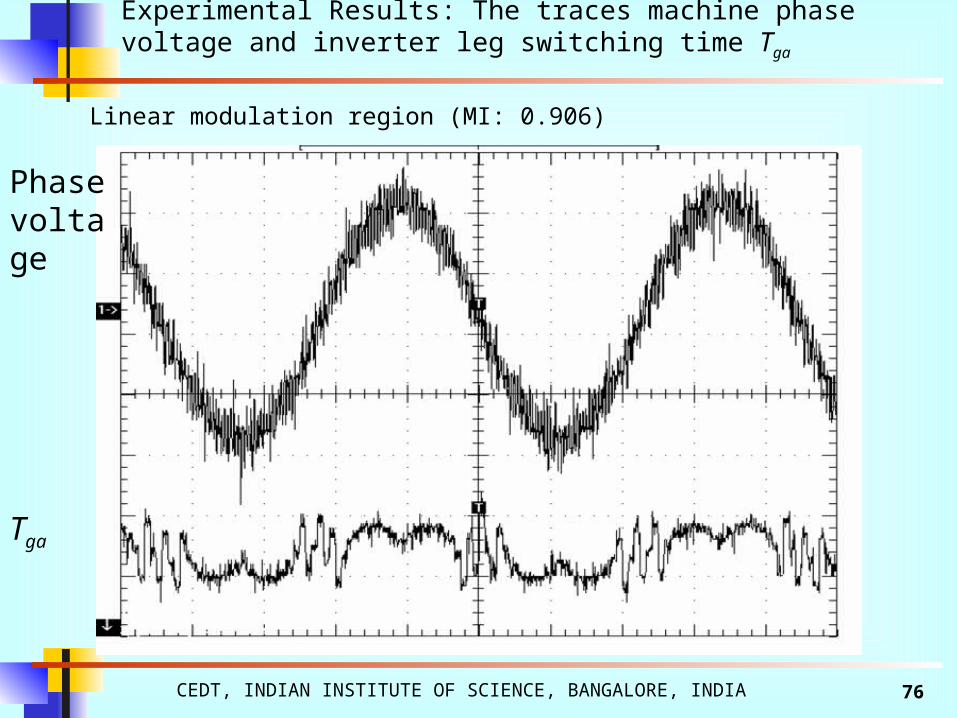
Phase voltage
Tga
Linear modulation region (MI: 0.906)
Experimental Results: The traces machine phase voltage and inverter leg switching time Tga

CEDT, INDIAN INSTITUTE OF SCIENCE, BANGALORE, INDIA 77
Phase voltage
Tga
Over-Modulation Region (MI: 0.926)
Experimental Results: The traces machine phase voltage and inverter leg switching time Tga
CEDT, INDIAN INSTITUTE OF SCIENCE, BANGALORE, INDIA 79
Phase voltage
Tga
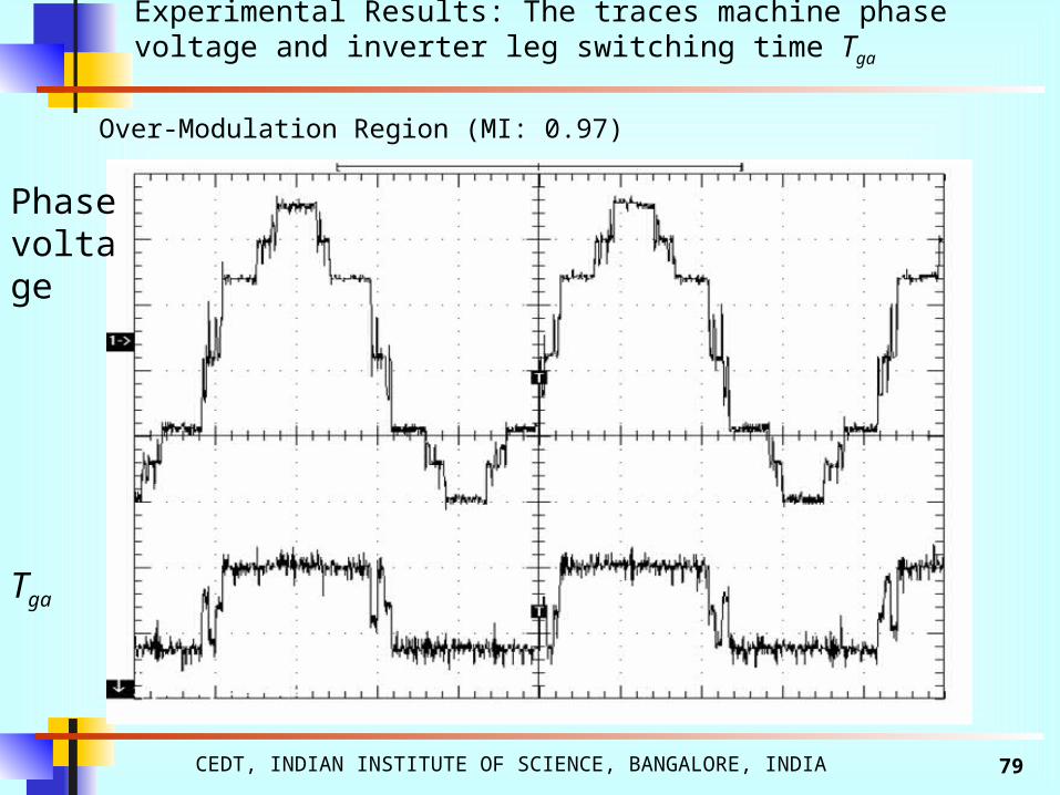
Over-Modulation Region (MI: 0.97)
Experimental Results: The traces machine phase voltage and inverter leg switching time Tga

CEDT, INDIAN INSTITUTE OF SCIENCE, BANGALORE, INDIA 80
Phase voltage
Tga
Square wave switching mode (MI: 1.00)
Experimental Results: The traces machine phase voltage and inverter leg switching time Tga
CEDT, INDIAN INSTITUTE OF SCIENCE, BANGALORE, INDIA 81
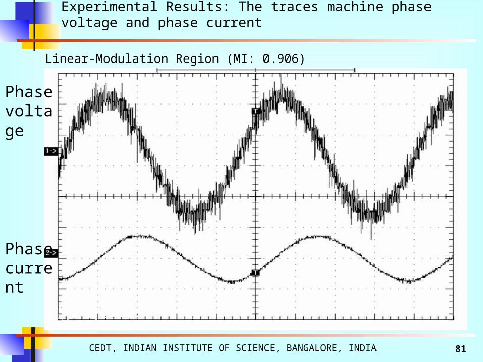
Phase voltage
Phase current
Linear-Modulation Region (MI: 0.906)
Experimental Results: The traces machine phase voltage and phase current

CEDT, INDIAN INSTITUTE OF SCIENCE, BANGALORE, INDIA 82
Phase voltage
Phase current
Linear-Modulation Region (MI: 0.93)
Experimental Results: The traces machine phase voltage and phase current

CEDT, INDIAN INSTITUTE OF SCIENCE, BANGALORE, INDIA 83
Phase voltage
Phase current
Linear-Modulation Region (MI: 0.957)
Experimental Results: The traces machine phase voltage and phase current

CEDT, INDIAN INSTITUTE OF SCIENCE, BANGALORE, INDIA 84
Phase voltage
Phase current
Linear-Modulation Region (MI: 0.97)
Experimental Results: The traces machine phase voltage and phase current
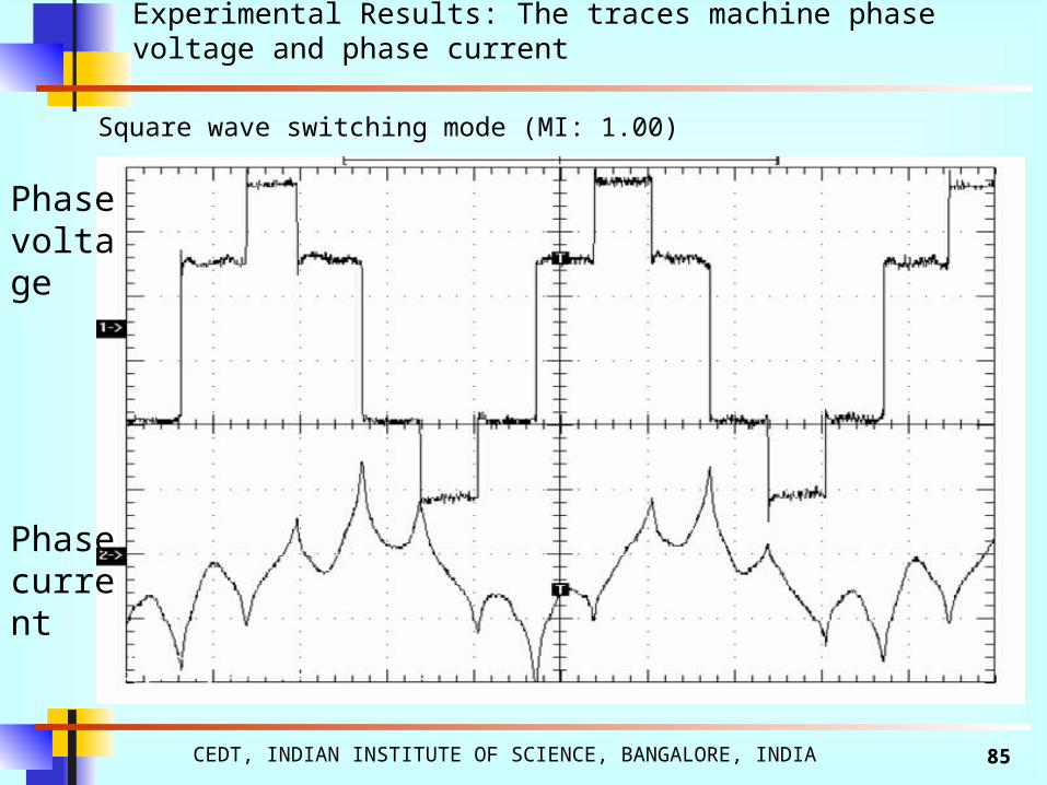
CEDT, INDIAN INSTITUTE OF SCIENCE, BANGALORE, INDIA 85
Phase voltage
Phase current
Square wave switching mode (MI: 1.00)
Experimental Results: The traces machine phase voltage and phase current

CEDT, INDIAN INSTITUTE OF SCIENCE, BANGALORE, INDIA 86
Experimental Results: Transition from Linear to square wave switching mode
Top Trace: time equivalent of modified reference signals T*as
Bottom Trace: Inverter gate switching time Tga

CEDT, INDIAN INSTITUTE OF SCIENCE, BANGALORE, INDIA 87
Experimental Results: Transition from Linear to six-step mode
Top Trace: Phase voltage, Bottom Trace: Phase current

CEDT, INDIAN INSTITUTE OF SCIENCE, BANGALORE, INDIA 88
Fundamental output voltage as a function of modulation index-MI
0 10 20 30 40 50 60 70 80 90 1000
0.1
0.2
0.3
0.4
0.5
0.6
0.7
0.8
0.9
1
MI (%)
Vfu
nd(P
.U.)

CEDT, INDIAN INSTITUTE OF SCIENCE, BANGALORE, INDIA 89
90 92 94 96 98 1000
0.05
0.1
0.15
0.2
0.25
MI (%)
nth H
arm
on
ic (
P.U
.)
571113
Harmonic components in the output waveform in the over-modulation region

CEDT, INDIAN INSTITUTE OF SCIENCE, BANGALORE, INDIA 90
Linearization of the Multi-level SVPWM in the Over-Modulation Region
• A simple n-level PWM signal generation with linear voltage transfer characteristics throughout the modulation range, up to six-step mode of operation
• Linear voltage transfer characteristics in the over-modulation region is achieved by modifying the reference signal such that• the modified reference signal has the same fundamental component as
the original reference signal • modified reference signals are always within the carrier region
• Inverter leg switching times are directly obtained from the sampled amplitudes of reference phase voltages signals
• Does not require any sector identification, sine look-up tables for switching vector identification
• Does not use sector mapping or complex timing calculations
SUMMARY:

Twelve-sided polygonal voltage space vector based multilevel inverter for induction motors.

CEDT, INDIAN INSTITUTE OF SCIENCE, BANGALORE, INDIA 92
Topology of a multilevel inverter for generation of 12-side polygonal voltage space vectors for induction motor drives.

CEDT, INDIAN INSTITUTE OF SCIENCE, BANGALORE, INDIA 93
Generation of voltage space vectors

CEDT, INDIAN INSTITUTE OF SCIENCE, BANGALORE, INDIA 94
0 0 0 01 2. (( 1).30 15 ) . ( .30 15 ) .( )ST V m T V m T V jV
0 0 0 01 2. ( 1).30 . .30 .( ).( 15 15 )ST V m T V m T V jV Cos jSin
0 0 0 01
2. . ( .30 15 ) . ( .30 15 )ST
T V Sin m V Cos mV
0 0 0 02
2. . (( 1).30 15 ) . (( 1).30 15 )ST
T V Sin m V Cos mV
0 0 0 01
2 3.. . ( .30 15 ) . ( .30 45 )S
B C
TT v Sin m v Cos m
V
0 0 0 02
2 3.. . (( 1).30 15 ) . (( 1).30 45 )S
B C
TT v Sin m v Cos m
V

CEDT, INDIAN INSTITUTE OF SCIENCE, BANGALORE, INDIA 95
‘Va’ positive ‘Vb-Vc’ positive: 1st quadrant
‘Va’ negative ‘Vb-Vc’ positive: 2nd quadrant
‘Va’ negative ‘Vb-Vc’ negative: 3rd quadrant
‘Va’ positive ‘Vb-Vc’ negative: 4th quadrant

CEDT, INDIAN INSTITUTE OF SCIENCE, BANGALORE, INDIA 96
If in quadrant 1:
If |Vb-Vc|<=|Va|.√3.tan150 then sector 1 else
If |Vb-Vc|<=|Va|.√3.tan450 then sector 2 else
If |Vb-Vc|<=|Va|.√3.tan750 then sector 3
else sector 4
If in quadrant 2:If |Vb-Vc|<=|Va|.√3.tan150 then sector 7 elseIf |Vb-Vc|<=|Va|.√3.tan450 then sector 6 elseIf |Vb-Vc|<=|Va|.√3.tan750 then sector 5 else sector 4

CEDT, INDIAN INSTITUTE OF SCIENCE, BANGALORE, INDIA 97
If in quadrant 3:If |Vb-Vc|<=|Va|.√3.tan150 then sector 7 elseIf |Vb-Vc|<=|Va|.√3.tan450 then sector 8 elseIf |Vb-Vc|<=|Va|.√3.tan750 then sector 9 else sector 10
If in quadrant 4:If |Vb-Vc|<=|Va|.√3.tan150 then sector 1 elseIf |Vb-Vc|<=|Va|.√3.tan450 then sector 12 elseIf |Vb-Vc|<=|Va|.√3.tan750 then sector 11 else sector 10
CEDT, INDIAN INSTITUTE OF SCIENCE, BANGALORE, INDIA 98
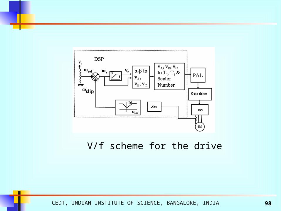
V/f scheme for the drive

CEDT, INDIAN INSTITUTE OF SCIENCE, BANGALORE, INDIA 99
Comparison to obtain time durations

CEDT, INDIAN INSTITUTE OF SCIENCE, BANGALORE, INDIA 100
Pole voltage at 30Hz.
• Voltage levels at 0.366Vdc, 1.0Vdc and 1.366Vdc are observed.

CEDT, INDIAN INSTITUTE OF SCIENCE, BANGALORE, INDIA 101
Phase voltage at 30Hz.
CEDT, INDIAN INSTITUTE OF SCIENCE, BANGALORE, INDIA 102
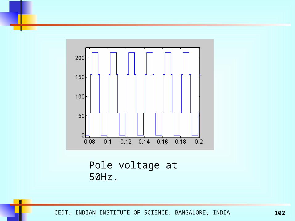
Pole voltage at 50Hz.

CEDT, INDIAN INSTITUTE OF SCIENCE, BANGALORE, INDIA 103
Phase voltage at 50Hz.

CEDT, INDIAN INSTITUTE OF SCIENCE, BANGALORE, INDIA 104
Fig. 14a: Phase voltage and motor current at 15Hz. (X-axis: 1div=20ms, Y-axis: 1div=100V)
Fig. 14b: Pole voltage at 15Hz. (X-axis: 1div=20ms, Y-axis:1div=50V)

CEDT, INDIAN INSTITUTE OF SCIENCE, BANGALORE, INDIA 105
Fig. 15a: Phase voltage and motor current at 30Hz. (X-axis: 1div=10ms, Y-axis: 1div=50V)
Fig. 15b: Pole voltage and motor current at 30Hz.(X-axis: 1div=5ms, Y-axis: 1div=50V)

CEDT, INDIAN INSTITUTE OF SCIENCE, BANGALORE, INDIA 106
Fig. 16a: Phase voltage and motor current at 45Hz.(X-axis: 1div=10ms, Y-axis: 1div=100V)
Fig. 16b: Pole voltage at 45Hz. (X-axis: 1div=10ms, Y-axis: 1div=50V)

CEDT, INDIAN INSTITUTE OF SCIENCE, BANGALORE, INDIA 107
Fig. 17a: Phase voltage and motor current at 50Hz.(X-axis: 1div=5ms, Y-axis: 1div=100V)
Fig. 17b: Pole voltage at 50Hz.(X-axis: 1div=5ms, Y-axis:1div=50V)
CEDT, INDIAN INSTITUTE OF SCIENCE, BANGALORE, INDIA 108
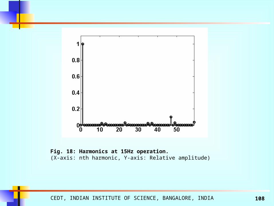
Fig. 18: Harmonics at 15Hz operation. (X-axis: nth harmonic, Y-axis: Relative amplitude)
CEDT, INDIAN INSTITUTE OF SCIENCE, BANGALORE, INDIA 109
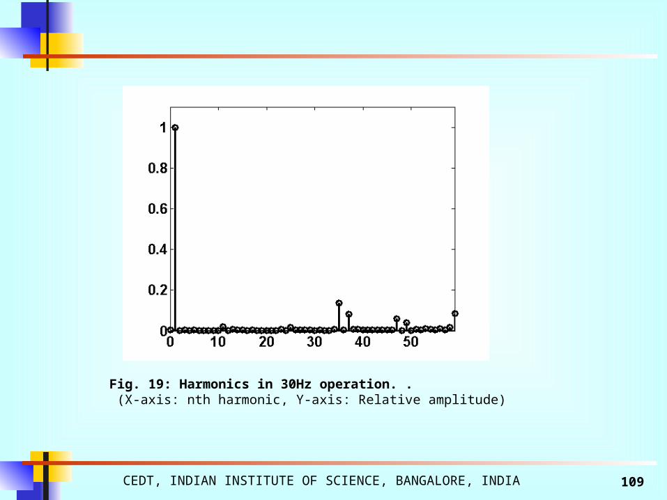
Fig. 19: Harmonics in 30Hz operation. . (X-axis: nth harmonic, Y-axis: Relative amplitude)

CEDT, INDIAN INSTITUTE OF SCIENCE, BANGALORE, INDIA 110
Fig. 20: Harmonics in 45Hz operation. (X-axis: nth harmonic, Y-axis: Relative amplitude)

CEDT, INDIAN INSTITUTE OF SCIENCE, BANGALORE, INDIA 111
Fig. 21: Harmonics in 50Hz operation. . (X-axis: nth harmonic, Y-axis: Relative amplitude)

CEDT, INDIAN INSTITUTE OF SCIENCE, BANGALORE, INDIA 112
Control of Switching Frequency Variation inHysteresis Controller for IM Drives Using
Variable Parabolic Bands for CurrentError Space Phasor

CEDT, INDIAN INSTITUTE OF SCIENCE, BANGALORE, INDIA 113
• Common problems associated with the conventional, as well as current error space phasor based hysteresis controllers with fixed bands (boundaries), are the wide variation of switching frequency in a fundamental output cycle and variation of switching frequency with the variation in the speed of the load motor.
• These problems cause increased switching looses in the inverter, non-optimum current ripple, and excess harmonics in the load current, which leads to additional heating in the motor.
Problem of Switching Frequency Variation
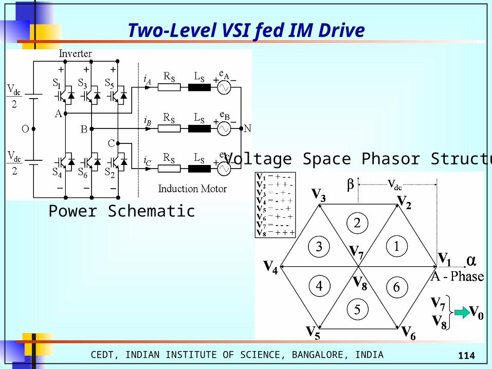
CEDT, INDIAN INSTITUTE OF SCIENCE, BANGALORE, INDIA 114
Two-Level VSI fed IM Drive
Power Schematic
Voltage Space Phasor Structure

Start of the Sector Middle of the Sector
End of the Sector
k mΔi V Vd
dt L
Directions of Current Error Space Phasor When Different Voltage Vectors are Switched for Different Positions of Vm in Sector-1
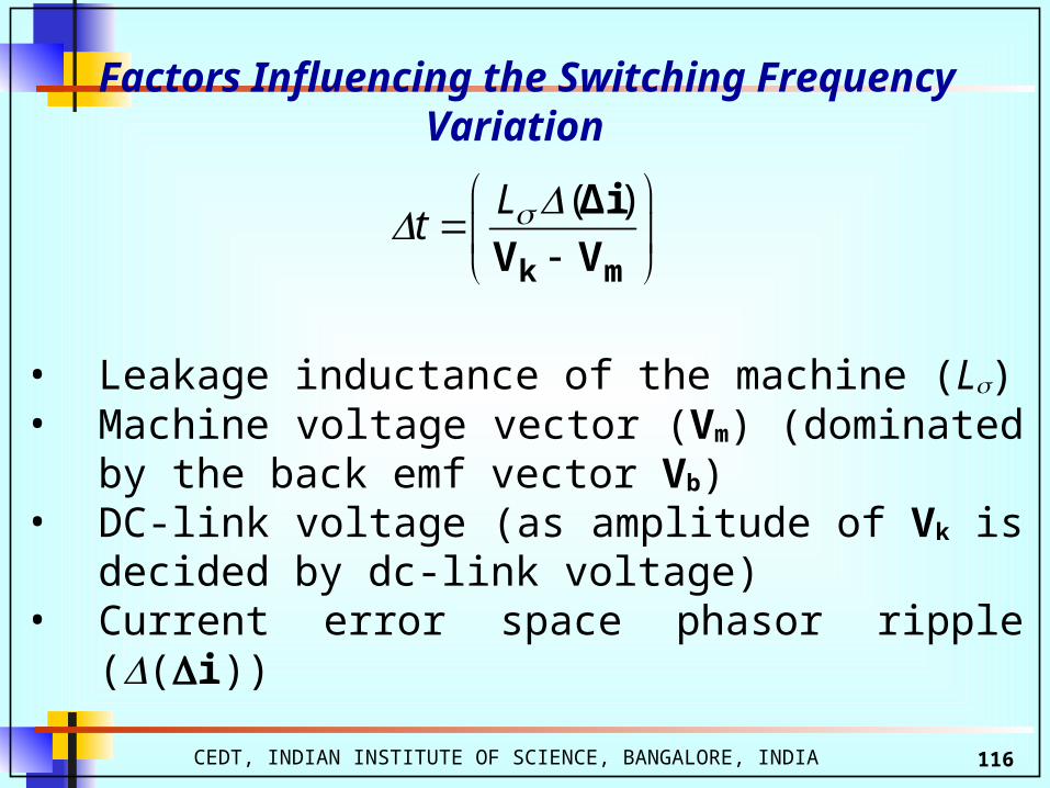
CEDT, INDIAN INSTITUTE OF SCIENCE, BANGALORE, INDIA 116
• Leakage inductance of the machine (L)• Machine voltage vector (Vm) (dominated by the back
emf vector Vb)• DC-link voltage (as amplitude of Vk is decided by dc-
link voltage) • Current error space phasor ripple ((i))
Factors Influencing the Switching Frequency Variation
( )
k m
Δi
V V
Lt

CEDT, INDIAN INSTITUTE OF SCIENCE, BANGALORE, INDIA 117
• Over a fundamental period, the position of Vm varies with respect to the inverter voltage vectors of space phasor structure.
• Also, the selected inverter voltage vector Vk (V1, …, V8) keeps on changing in a fundamental cycle during hysteresis PWM current control.
• Therefore, either the inverter switching frequency or/and the current error space phasor ripple will vary over a fundamental inverter period.
Variation of Switching Frequency inHysteresis Current Controller
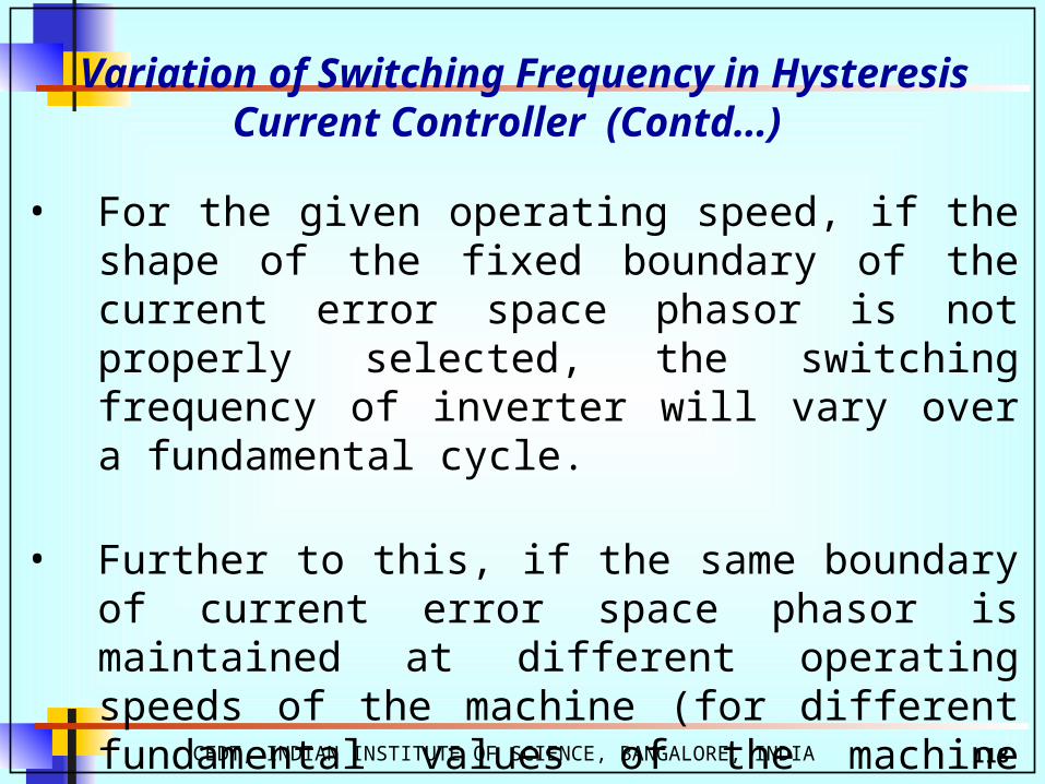
CEDT, INDIAN INSTITUTE OF SCIENCE, BANGALORE, INDIA 118
• For the given operating speed, if the shape of the fixed boundary of the current error space phasor is not properly selected, the switching frequency of inverter will vary over a fundamental cycle.
• Further to this, if the same boundary of current error space phasor is maintained at different operating speeds of the machine (for different fundamental values of the machine back emf) then also the inverter switching frequency will vary.
Variation of Switching Frequency in HysteresisCurrent Controller (Contd…)

CEDT, INDIAN INSTITUTE OF SCIENCE, BANGALORE, INDIA 119
Investigation of Current Error Space Phasor inVC-SVPWM based VSI fed IM Drives
Typical SVPWMswitching pattern
of the invertervoltage vectors
for two consecutivePWM
switching intervals
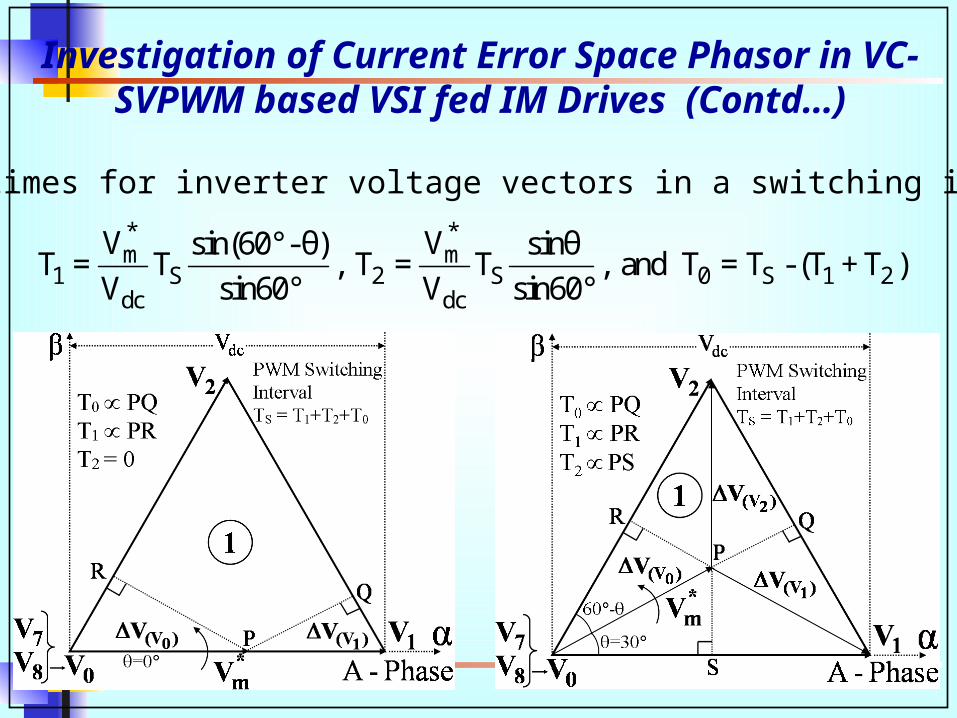
Investigation of Current Error Space Phasor in VC-SVPWM based VSI fed IM Drives (Contd…)
* *m m
1 S 2 S 0 S 1 2dc dc
V Vsin(60° -θ) sinθT = T , T = T , and T = T - (T + T )
V sin60° V sin60°
Switching times for inverter voltage vectors in a switching interval
Investigation of Current Error Space Phasor in VC-SVPWM based VSI fed IM Drives (Contd…)
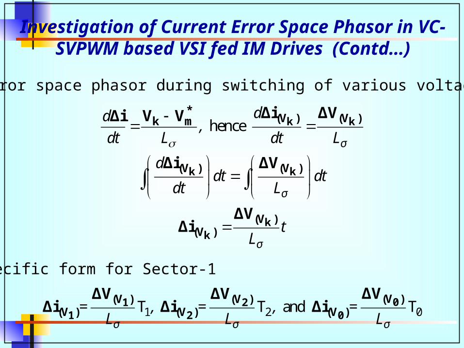
Current error space phasor during switching of various voltage vectors
hence k k
k k
kk
*(V ) (V )k m
(V ) (V )
(V )(V )
Δi ΔVV VΔi
Δi ΔV
ΔVΔi
σ
σ
σ
dd,
dt L dt L
ddt dt
dt L
tL
Specific form for Sector-1
1 2 0T T and T01 21 2 0
(V )(V ) (V )(V ) (V ) (V )
ΔVΔV ΔVΔi Δi Δi
σ σ σ
= , = , =L L L

Movement of current error space phasor (on - plane) in a few sampling intervals of VC-SVPWM based two-level VSI fed IM drive
[Y-axisAnd
X-axis:Current
InAmperes]
Vm at start of the sector( varies from 0 to 7)
Vm at middle of the sector( varies from 27 to 33)
Vm at end of the sector( varies from 54 to 60)

Approximate theoretical boundary of i for VC-SVPWM based two-level VSI fed IM drive for position of Vm in Sector-1
[Y-axisAnd
X-axis:Current
InAmperes]
10 Hz 20 Hz
30 Hz 40 Hz
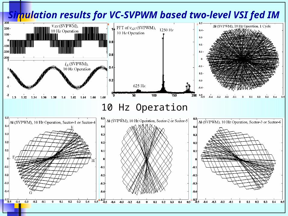
Simulation results for VC-SVPWM based two-level VSI fed IM drive
10 Hz Operation
Simulation results for VC-SVPWM based two-level VSI fed IM drive
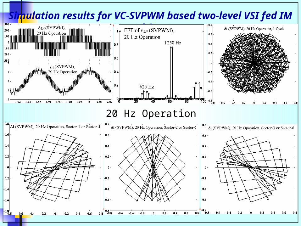
20 Hz Operation

Simulation results for VC-SVPWM based two-level VSI fed IM drive
30 Hz Operation
Simulation results for VC-SVPWM based two-level VSI fed IM drive
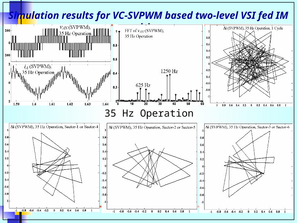
35 Hz Operation

Simulation results for VC-SVPWM based two-level VSI fed IM drive
41 Hz Operation

Comparison of boundary obtained by theoretical calculations and simulation studies for VC-SVPWM based two-level VSI fed IM drive
10 Hz 20 Hz 30 Hz 40 Hz0.1 A/div. 0.2 A/div. 0.2 A/div. 0.5 A/div.
Theoretical
Simulation
Establishing variable boundary for proposed hysteresis controller
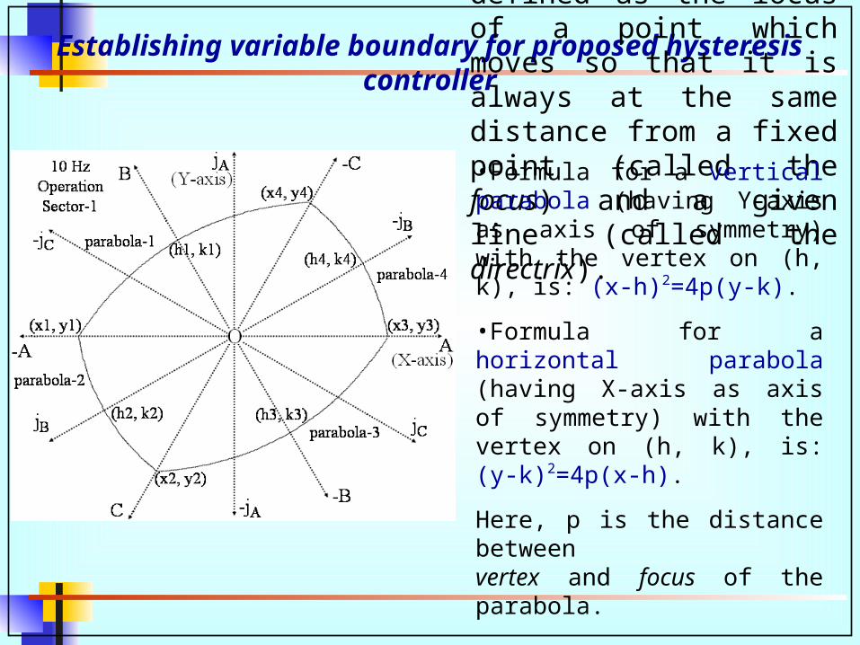
The parabola is defined as the locus of a point which moves so that it is always at the same distance from a fixed point (called the focus) and a given line (called the directrix).
•Formula for a vertical parabola (having Y-axis as axis of symmetry) with the vertex on (h, k), is: (x-h)2=4p(y-k).
•Formula for a horizontal parabola (having X-axis as axis of symmetry) with the vertex on (h, k), is: (y-k)2=4p(x-h).
Here, p is the distance betweenvertex and focus of the parabola.
CEDT, Indian Institute of Science, Bangalore, INDIA CEDT, INDIAN INSTITUTE OF SCIENCE, BANGALORE, INDIA
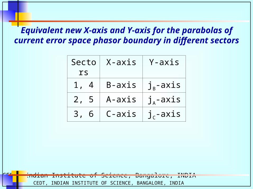
Equivalent new X-axis and Y-axis for the parabolas of current error space phasor boundary in different sectors
Sectors X-axis Y-axis
1, 4 B-axis jB-axis
2, 5 A-axis jA-axis
3, 6 C-axis jC-axis

CEDT, Indian Institute of Science, Bangalore, INDIA CEDT, INDIAN INSTITUTE OF SCIENCE, BANGALORE, INDIA
Generalized technique to find the parameters of the boundary defining parabolas for given induction motor
Generalized Technique(Matlab Program)
Developed in Proposed Work
input output
(x, y),(h, k),
pFor boundary
defining parabolasfor operating
frequencyfrom 1 Hz to 45 Hzwith the resolution
of 1 Hz
Vdc,Base_freq,
L,TS,

Boundary for proposed hysteresis controller with new reference axis
1
2
0
22(V ) m dc m dc
22(V ) m dc m dc
(V ) m
ΔV = V + V - 2 V V cosθ
ΔV = V + V - 2 V V cos(60° - θ)
ΔV = V
0
0
(V )0
(V ) σ
=0
=0
ΔVTΔi L
x1_new = sin30 = sin302 2
0
0
(V )0
(V ) σ
=0
=0
ΔVTΔi L
y1_new = cos30 = cos302 2
0
0
(V )0
(V ) σ
=30
=30
ΔVTΔi L
k2_new = =2 2
0
2
0
1
22 (V )
(V ) θ=30°θ=30°
22 (V )
(V ) θ=30°θ=30°
Δih1_new = Δi -
2
Δih3_new = Δi -
2
dcm
(ope_freq)
ope_freq in Hz x 0.955VV =
50 Hz

CEDT, Indian Institute of Science, Bangalore, INDIA CEDT, INDIAN INSTITUTE OF SCIENCE, BANGALORE, INDIA
Parameters of boundary defining parabolasfor proposed hysteresis controller
2
2
2
2
p1 = (y1_new - k1_new) 4(x1_new - h1_new)
p2 = (x2_new - h2_new) 4(y2_new - k2_new)
p3 = (y3_new - k3_new) 4(x3_new - h3_new)
p4 = (x4_new - h4_new) 4(y4_new - k4_new)
x1_new, y1_new h1_new,k1_new
x2_new, y2_new h2_new,k2_new
x3_new, y3_new h3_new,k3_new
x4_new, y4_new h4_new,k4_new

Output of the generalized technique in terms of parameters of boundary defining parabolas

Output of the generalized technique in terms of the current error space phasor boundary for different operating frequencies
[conventional Y-axis and X-axis: 1div.=0.5 A]
CEDT, Indian Institute of Science, Bangalore, INDIA CEDT, INDIAN INSTITUTE OF SCIENCE, BANGALORE, INDIA
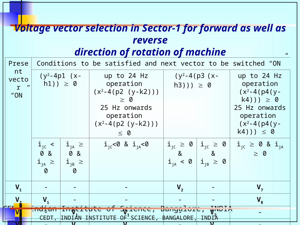
Voltage vector selection in Sector-1 for forward as well as reversedirection of rotation of machine
Present vector“ON”
Conditions to be satisfied and next vector to be switched “ON”
(y2-4p1 (x-h1)) 0
up to 24 Hz operation (x2-4(p2 (y-k2))) 0
25 Hz onwards operation (x2-4(p2 (y-k2))) 0
(y2-4(p3 (x-h3))) 0 up to 24 Hz operation
(x2-4(p4(y-k4))) 0
25 Hz onwards operation
(x2-4(p4(y-k4))) 0
ijC 0 &
ijA 0
ijA 0
&ijB 0
ijC0 & ijA0 ijC 0
&ijA 0
ijC 0
&ijB 0
ijC 0 & ijA 0
V1 - - - V2 - V7
V2 V1 - - - - V8
V7 - V1 V1 - V2 -
V8 - V1 V2 - V2 -
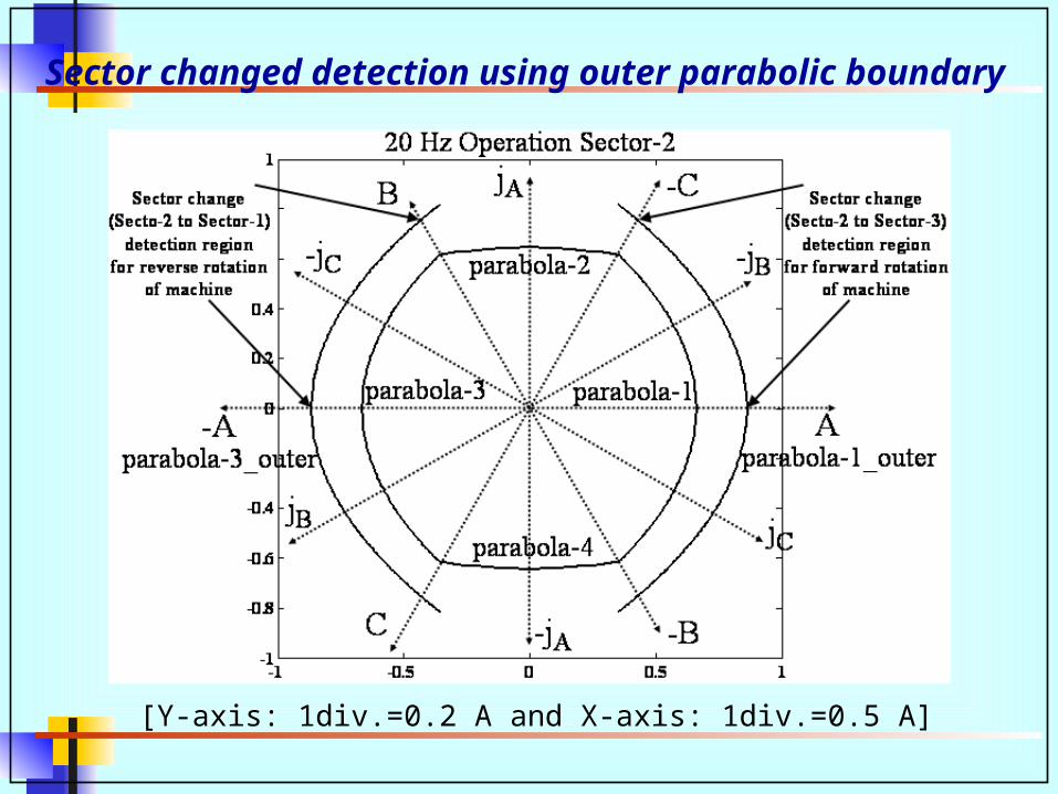
Sector changed detection using outer parabolic boundary
[Y-axis: 1div.=0.2 A and X-axis: 1div.=0.5 A]
CEDT, Indian Institute of Science, Bangalore, INDIA CEDT, INDIAN INSTITUTE OF SCIENCE, BANGALORE, INDIA
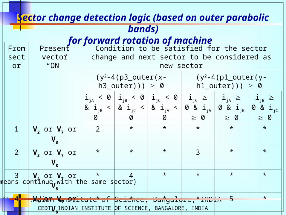
Sector change detection logic (based on outer parabolic bands)for forward rotation of machine
From sector
Presentvector “ON”
Condition to be satisfied for the sector change and next sector to be considered as new sector
(y2-4(p3_outer(x-h3_outer))) 0
(y2-4(p1_outer(y-h1_outer))) 0
ijA < 0 &
ijB < 0
ijB < 0 &
ijC < 0
ijC < 0 &
ijA < 0
ijC 0 &
ijA 0
ijA 0 &
ijB 0
ijB 0 &
ijC 0
1 V2 or V7 or V8 2 * * * * *
2 V3 or V7 or V8 * * * 3 * *
3 V4 or V7 or V8 * 4 * * * *
4 V5 or V7 or V8 * * * * 5 *
5 V6 or V7 or V8 * * 6 * * *
6 V1 or V7 or V8 * * * * * 1(‘*’ means continue with the same sector)
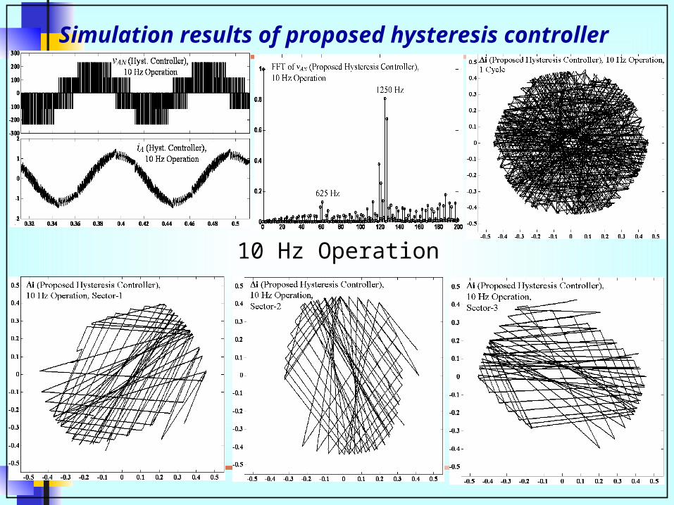
Simulation results of proposed hysteresis controller
10 Hz Operation

Simulation results of proposed hysteresis controller
10 Hz Operation

Simulation results of proposed hysteresis controller
20 Hz Operation

Simulation results of proposed hysteresis controller
20 Hz Operation

Simulation results of proposed hysteresis controller
30 Hz Operation

CEDT, Indian Institute of Science, Bangalore, INDIA CEDT, INDIAN INSTITUTE OF SCIENCE, BANGALORE, INDIA
Simulation results of proposed hysteresis controller
30 Hz Operation
Simulation results of proposed hysteresis controller
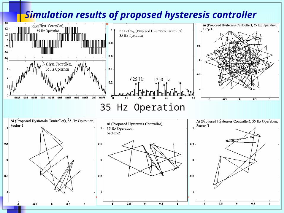
35 Hz Operation

CEDT, Indian Institute of Science, Bangalore, INDIA CEDT, INDIAN INSTITUTE OF SCIENCE, BANGALORE, INDIA
Simulation results of proposed hysteresis controller
35 Hz Operation

Simulation results of proposed hysteresis controller
40 Hz Operation

Comparison of boundary obtained by theoretical calculations and simulation studies for VC-SVPWM based two-level VSI fed IM drive
10 Hz 30 Hz 35 Hz 40 Hz
SVPWM Simulation
Proposed Hysteresis Controller Simulation

CEDT, Indian Institute of Science, Bangalore, INDIA CEDT, INDIAN INSTITUTE OF SCIENCE, BANGALORE, INDIA
Simulation results of proposed hysteresis controller
47 Hz Operation
Simulation results of proposed hysteresis controller
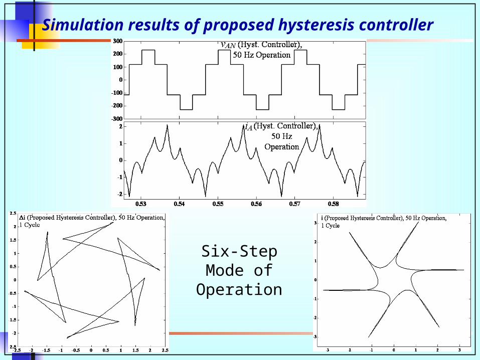
Six-Step Mode of Operation

CEDT, Indian Institute of Science, Bangalore, INDIA CEDT, INDIAN INSTITUTE OF SCIENCE, BANGALORE, INDIA
Block schematic of experimental set-up used for proposedhysteresis controller

Experimental results of proposed hysteresis controller
10 Hz Operation
vAN, 130 V/div.
iA, 1.3 A/div.
i, Sector-1 i, Sector-2 i, Sector-3
i, 0.2 A/div.

CEDT, Indian Institute of Science, Bangalore, INDIA CEDT, INDIAN INSTITUTE OF SCIENCE, BANGALORE, INDIA
Experimental results of proposed hysteresis controller
10 Hz Operation
iA, 1.3 A/div.
iA*, 1.3 A/div.
i, 1 A/div.
Experimental results of proposed hysteresis controller
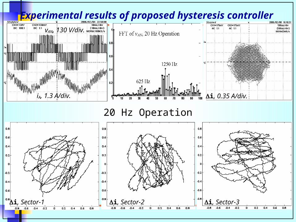
20 Hz Operation
vAN, 130 V/div.
iA, 1.3 A/div.
i, Sector-1 i, Sector-2 i, Sector-3
i, 0.35 A/div.

Experimental results of proposed hysteresis controller
20 Hz Operation
iA, 1.3 A/div.
iA, 1.3 A/div.
iA*, 1.3 A/div.
iA*, 1.3 A/div.
i, 1 A/div.

Experimental results of proposed hysteresis controller
30 Hz Operation
vAN, 135 V/div.
iA, 1.3 A/div.
i, Sector-1 i, Sector-2 i, Sector-3
i, 0.45 A/div.

Experimental results of proposed hysteresis controller
30 Hz Operation
iA*, 1.3 A/div.
iA, 1.3 A/div.
iA, 1.3 A/div.
iA*, 1.3 A/div.
i, Sector-3, 0.45 A/div.
i, 1 A/div.

Experimental results of proposed hysteresis controller
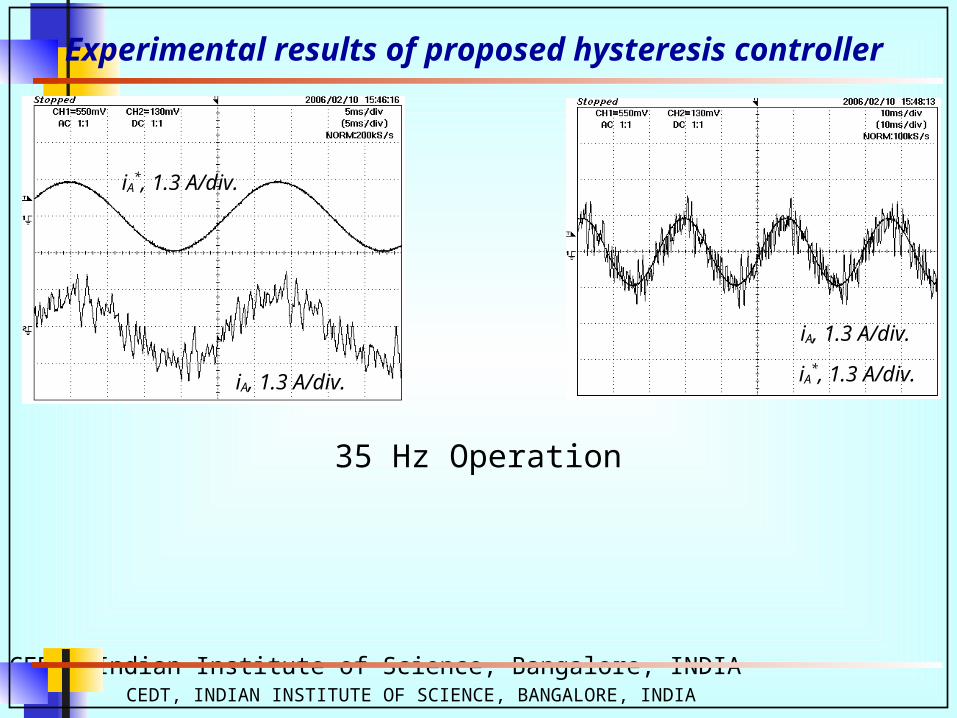
35 Hz Operation
vAN, 130 V/div.
iA, 1.3 A/div. i, 0.55 A/div.
i, Sector-2, 0.55 A/div. i, Sector-3, 0.55 A/div. i, Sector-3-4, 0.55 A/div.
CEDT, Indian Institute of Science, Bangalore, INDIA CEDT, INDIAN INSTITUTE OF SCIENCE, BANGALORE, INDIA
Experimental results of proposed hysteresis controller
35 Hz Operation
iA*, 1.3 A/div.
iA, 1.3 A/div.
iA, 1.3 A/div.
iA*, 1.3 A/div.

Experimental results of proposed hysteresis controller
40 Hz Operation
vAN, 130 V/div.
iA, 1.3 A/div.
i, Sector-1, 0.6 A/div. i, Sector-2, 0.6 A/div. i, Sector-3, 0.6 A/div.
i, 0.6 A/div.

Experimental results of proposed hysteresis controller
40 Hz Operation
iA, 1.3 A/div.
iA*, 1.3 A/div.
iA, 1.3 A/div.
iA*, 1.3 A/div.
i, Sector-4-5, 0.6 A/div.
CEDT, Indian Institute of Science, Bangalore, INDIA CEDT, INDIAN INSTITUTE OF SCIENCE, BANGALORE, INDIA
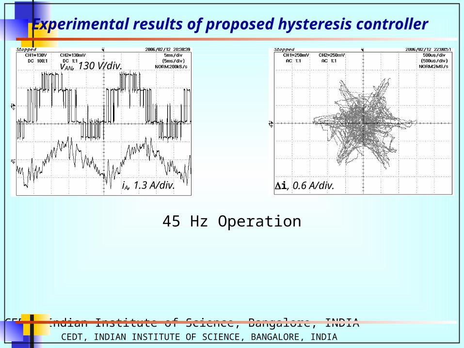
Experimental results of proposed hysteresis controller
45 Hz Operation
vAN, 130 V/div.
iA, 1.3 A/div. i, 0.6 A/div.

CEDT, Indian Institute of Science, Bangalore, INDIA CEDT, INDIAN INSTITUTE OF SCIENCE, BANGALORE, INDIA
Experimental results of proposed hysteresis controller
47 Hz Operation
vAN, 130 V/div.
iA, 1.3 A/div. i, 0.5 A/div.

Experimental results of proposed hysteresis controller
50 Hz Operation(Six-Step Mode)
vAN, 130 V/div.
iA, 1.3 A/div.
i, 0.65 A/div. i, 1.4 A/div.
Experimental results of proposed hysteresis controller
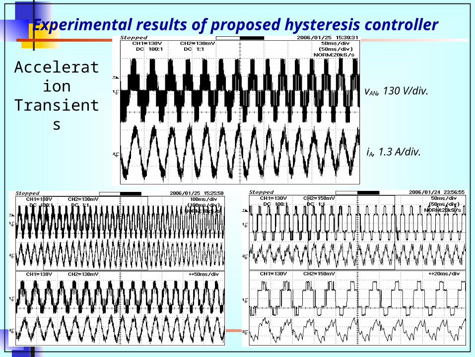
Acceleration Transients
vAN, 130 V/div.
iA, 1.3 A/div.

Experimental results of proposed hysteresis controller
Starting Operation
vAN, 160 V/div.
iA, 1.3 A/div.
iA, 1.5 A/div.
iA*, 1.5 A/div.
iA, 1.7 A/div.
speed, 910 rpm//div.

Experimental results of proposed hysteresis controller
Starting Operation
vAN, 160 V/div.
iA, 1.3 A/div.
iA*, 1.5 A/div.
iA, 1.5 A/div.
iA, 1.7 A/div.
speed, 910 rpm//div.

Experimental results of proposed hysteresis controller
Speed Reversal
vAN, 130 V/div.
iA, 1.1 A/div.
iA, 1.5 A/div.
iA, 1.35 A/div.
iA*, 1.35 A/div.
speed, 910 rpm//div.

Experimental results of proposed hysteresis controller
Speed Reversal
vAN, 130 V/div.
iA, 1.1 A/div.
iA, 1.5 A/div.
iA*, 1.5 A/div.
iA, 1.65 A/div.
speed, 910 rpm//div.

CEDT, INDIAN INSTITUTE OF SCIENCE, BANGALORE, INDIA 171
• Current error space phasor based simple hysteresis controller
• Controls the switching frequency variation in a two-level VSI fed IM drive
• Based on the novel concept of on-line variation of hysteresis band, depending upon the speed of the machine
• Uses parabolic boundary for the current error space phasor
• Obtains switching frequency spectrum in the output voltage similar to that of the constant switching frequency VC-SVPWM based VSI fed IM drive.
Salient features of the proposed hysteresis controller
CEDT, INDIAN INSTITUTE OF SCIENCE, BANGALORE, INDIA 172
• Performance of the proposed controller is independent of the load machine parameters
• The unique parabolic boundary for different operating speeds for any given induction motor is determined using generalized technique (Matlab program) developed in proposed work
• Calculation of machine back emf vector is not needed
• Sector change logic is self-adaptive and is capable of taking the drive up to six-step mode of operation, if needed
• Controller always selects the adjacent inverter voltage vectors, forming a sector, in which the tip of the machine voltage vector lies
Salient features of the proposed hysteresis controller(Contd…)

CEDT, INDIAN INSTITUTE OF SCIENCE, BANGALORE, INDIA 173
Multimotor drive setup
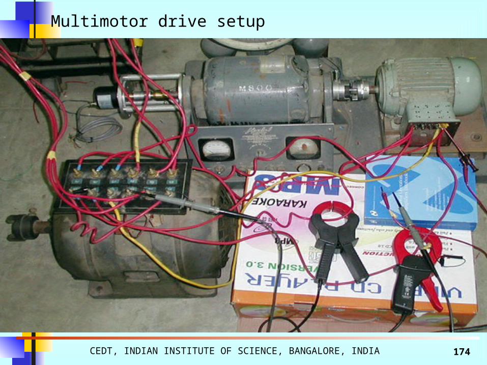
CEDT, INDIAN INSTITUTE OF SCIENCE, BANGALORE, INDIA 174
Multimotor drive setup

CEDT, INDIAN INSTITUTE OF SCIENCE, BANGALORE, INDIA 175

CEDT, INDIAN INSTITUTE OF SCIENCE, BANGALORE, INDIA 176
Inverter setup for multilevel structure

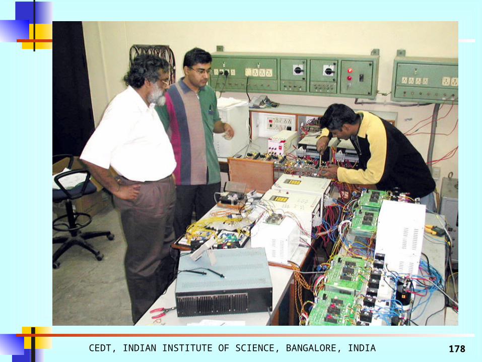
CEDT, INDIAN INSTITUTE OF SCIENCE, BANGALORE, INDIA 177
Inverter setup for multilevel structure
CEDT, INDIAN INSTITUTE OF SCIENCE, BANGALORE, INDIA 178

CEDT, INDIAN INSTITUTE OF SCIENCE, BANGALORE, INDIA 179
CEDT, INDIAN INSTITUTE OF SCIENCE, BANGALORE, INDIA 180

CEDT, INDIAN INSTITUTE OF SCIENCE, BANGALORE, INDIA 181