Embed Size (px)
Citation preview

YANG Ming-Chang
mcyang@cse
3943-8405
Room 906 SHB
WONG Kin Hong
khwong@cse
3943-8397
Room 907 SHB
VHDL 0 (v.7A) : Introduction 1
http://www.cse.cuhk.edu.hk/~mcyang/teaching.html
http://www.cse.cuhk.edu.hk/~khwong/www2/ceng3430/ceng3430.html
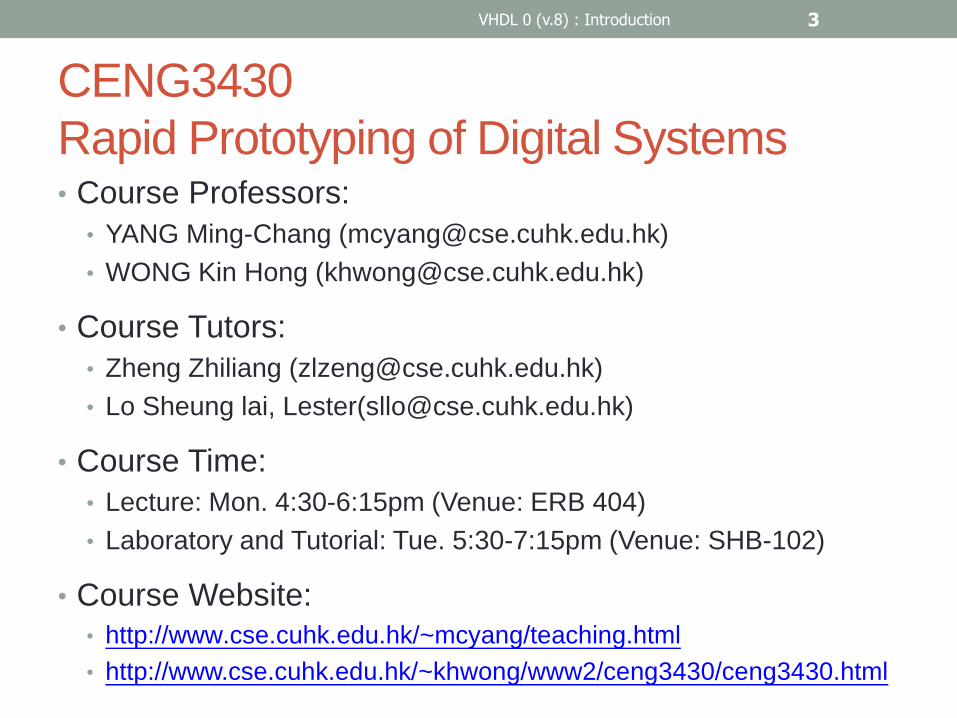
CENG3430
RAPID PROTOTYPING OF
DIGITAL SYSTEMS

CENG3430
Rapid Prototyping of Digital Systems
• You will learn:
• The hardware description language
• E.g., VHDL or Verilog
• Techniques to build a logic system
• E.g. Building blocks of a Central Processing Unit (CPU)
• High speed logic circuits analysis: time delay
estimation, testing, power supply stability, etc.
1 entity and2 is port (a,b : in std_logic;
2 c : out std_logic);
3 end and2
4 architecture and2_arch of and2
5 begin
6 c <=a and b;
7 end and2_arch
Write VHDL code, then it will generate the hardware chip automatically
Ex: VHDL AND-gate Program
VHDL 0 (v.7A) : Introduction 2
CENG3430
Rapid Prototyping of Digital Systems• Course Professors:
• YANG Ming-Chang ([email protected])
• WONG Kin Hong ([email protected])
• Course Tutors:
• Zheng Zhiliang ([email protected])
• Lo Sheung lai, Lester([email protected])
• Course Time:
• Lecture: Mon. 4:30-6:15pm (Venue: ERB 404)
• Laboratory and Tutorial: Tue. 5:30-7:15pm (Venue: SHB-102)
• Course Website:
• http://www.cse.cuhk.edu.hk/~mcyang/teaching.html
• http://www.cse.cuhk.edu.hk/~khwong/www2/ceng3430/ceng3430.html
VHDL 0 (v.8) : Introduction 3

CENG3430
Rapid Prototyping of Digital Systems
Weeks Date Lecture Lab
Week 1 Jan. 8~9 VHDL 0 & VHDL 1: Introduction No Lab
Week 2 Jan. 15~16 VHDL 2: Identifiers, Data Objects and Types Lecture
Week 3 Jan. 22~23 VHDL 3: Basic Operators and Arch. Body Introduce Vivado + Software Simulation
Week 4 Jan. 29~30 VHDL 4: Building Blocks of a Computer Implement OR Gate
Week 5 Feb. 5~6 VHDL 5: Finite State Machines Tri-state Logic + Simulation
Week 6 Feb. 12~13 VHDL 6: FSM Examples 4-to-1 Multiplexer
Week 7 Feb. 19~20 New Years New Years
Week 8 Feb. 26~27 VHDL 7: Use of Signals Serial-in-parallel-out Shift Register
Week 9 Mar. 5~6 VHDL 8: Application Examples Driving the Seven Segment Display
Week 10 Mar. 12~13 VHDL 9: Programmable Logic Families Software Stopwatch
Week 11 Mar. 19~20 New Applications on FPGAs Linux GPIO + LED
Week 12 Mar. 26~27 Free Project Project Consultations
Week 13 Apr. 2~3 Reading Week Reading Week
Week 14 Apr. 9~10 HS_i: Power Supply Systems Project Demo
Week 15 Apr. 16~17 HS_ii: Transmission Lines Project Demo
VHDL 0 (v.8) : Introduction 4
CENG3430
Rapid Prototyping of Digital Systems
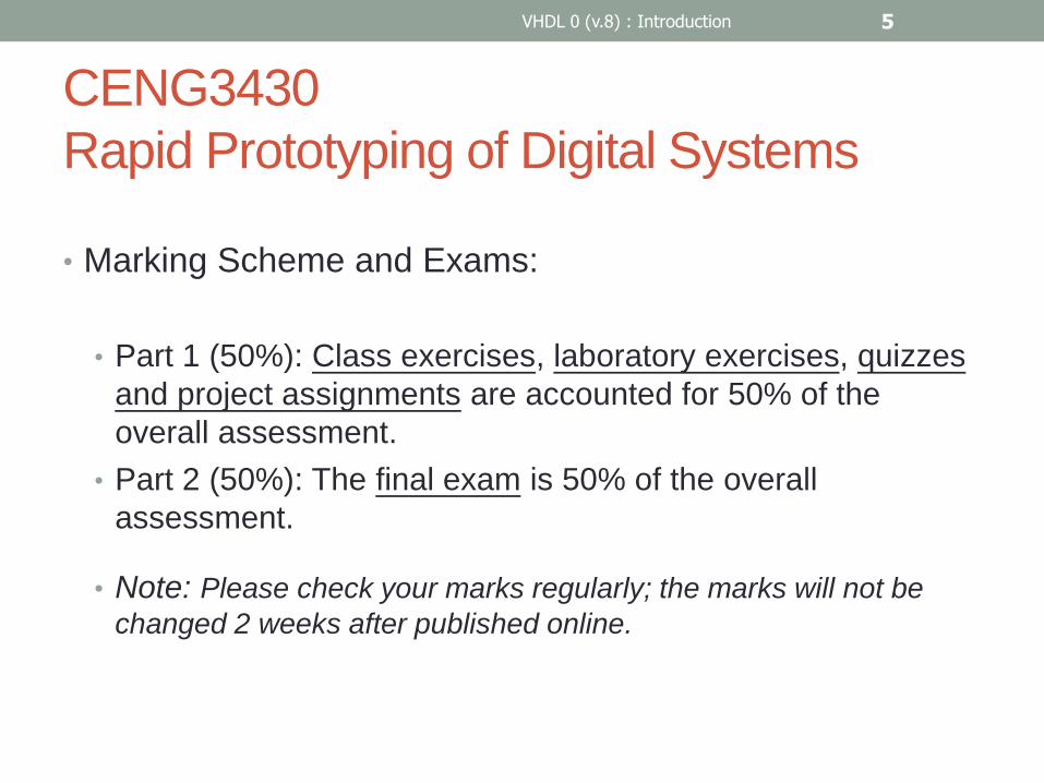
• Marking Scheme and Exams:
• Part 1 (50%): Class exercises, laboratory exercises, quizzes
and project assignments are accounted for 50% of the
overall assessment.
• Part 2 (50%): The final exam is 50% of the overall
assessment.
• Note: Please check your marks regularly; the marks will not be
changed 2 weeks after published online.
VHDL 0 (v.8) : Introduction 5

A QUICK RUN
THROUGHOverview
VHDL 0 (v.7A) : Introduction 6

Overview
•What is VHDL used for?
• To design
• Hardware systems (an industrial standard)
• Microprocessors: Arm7 etc.
• New digital systems: e.g. mobile phone, camera chips
VHDL 0 (v.7A) : Introduction 7

Motivations
• Learn to design digital systems.
• Provide knowledge for you to :
• Design products:
• Robots controllers, media players, portable games, mobile
phones.
• Advanced examples:
• Image processing
• Computer vision
• Super computer
• Start a business.
VHDL 0 (v.7A) : Introduction 8

Examples of Digital System Designs
• Mass products
• Media players
• Mobile phones
• Novel products
• Wearable devices
• Robots
• Research
• Real time edge detection for computer vision
• FPGA-based deep learning acceleration
VHDL 0 (v.7A) : Introduction 9

To learn
• Design digital processing components using
programmable logic.
VHDL 0 (v.7A) : Introduction 10
1 entity and2 is port (a,b : in std_logic;
2 c : out std_logic);
3 end and2
4 architecture and2_arch of and2
5 begin
6 c <=a and b;
7 end and2_arch
• Two existing Methods:
(a) Schematic
• Too complicated but is suitable
to describe the top level design
like a data flow block diagram.
(b) Language (e.g. VHDL--Very-
High-Speed-Integrated-Circuits
Hardware Description Language)
• Each module in the schematic
can be written in VHDL.

DIGITAL DESIGNWork Flow
VHDL 0 (v.7A) : Introduction 11

Digital Design Work Flow
• Idea generation
• Drafting on paper
• Design the chip (use VHDL)
• Test
• Manufacturing production line design
• Quality control
VHDL 0 (v.7A) : Introduction 12
1 entity and2 is port (a,b : in std_logic;
2 c : out std_logic);
3 end and2
4 architecture and2_arch of and2
5 begin
6 c <=a and b;
7 end and2_arch

WE USE IN OUR LAB
Hardware: FPGA (Field Programmable Gate Array)
The hardware can be reprogrammable, so you can change your design rapidly and easily with no additional hardware manufacturing cost.
Software: VHDL (Very-High-Speed-Integrated-Circuits Hardware Description Language)
VHDL 0 (v.7A) : Introduction 13

Re-programmable Hardware: FPGA
Field Programmable Gate Array
• What is inside an FPGA?
1) IOB: Input/Output Block
• Input/output of FPGA
2) CLB: Configurable Logic
Block (static ram based)
• Change the CLBs to get the
desired functions
3) Programmable
Interconnects
• Interconnect IOBs and CLBs
VHDL 0 (v.7A) : Introduction 14
From http://www.alldatasheet.co.kr/datasheet-
pdf/pdf_kor/49173/XILINX/XCS10-3PC84C.html

Inside a CLB (Configurable Logic block )
• The CLB is a fixed design but you can change the logic
function by reprogramming the bits in the logic function
lookup table.
• This will change the overall logic function of the CLB.
VHDL 0 (v.8) : Introduction 15
http://www.design-reuse.com/news_img/20100913_1.gifhttp://pldworld.biz/html/technote/pldesignline/bobz-02.gif
CLB
FPGA CLB (Configurable Logic block )

Software: To program an FPGA
VHDL 0 (v.7A) : Introduction 17
1 entity and2 is port (a,b : in std_logic;
2 c : out std_logic);
3 end and2
4 architecture and2_arch of and2
5 begin
6 c <=a and b;
7 end and2_arch
Use a schematic: (Top level
design to merge modules)
Use a language VHDL
(for each module)
or/and

Development cycle
VHDL 0 (v.8) : Introduction 18
1 entity and2 is port (a,b : in std_logic;
2 c : out std_logic);
3 end and2
4 architecture and2_arch of and2
5 begin
6 c <=a and b;
7 end and2_arch
VHDL LanguageSchematic (diagram)
Simulation

An example: “AND” gate in VHDL
VHDL 0 (v.8) : Introduction 19
• 1 entity and2 is port (a,b : in std_logic;
• 2 c : out std_logic);
• 3 end and2
• 4 architecture and2_arch of and2
• 5 begin
• 6 c <= a and b;
• 7 end and2_arch
a
bc
The chip
c <= a and b

Test bench and timing simulation
use simulation to see if your design is correct or not.
• See the tutorial at
http://www.cse.cuhk.edu.hk/~khwong/www2/ceng3430/CE
NG3430_1617_Tutorial_1_7a_test_bench.pptx
VHDL 0 (v.7A) : Introduction 20
You create some input patterns and see if the outputs are behaving correctly or not
Inputs
outputs

Summary of VHDL
• For hardware Design
• Parallel language (not sequential)
• Different! (not the same as C++ or Java)
• VHDL is the industrial standard for CE.
VHDL 0 (v.7A) : Introduction 21

COMPUTER
ENGINEERING MARKET
VHDL 0 (v.7A) : Introduction 22

TSMC (Taiwan Semicon. Manufacturing Comp.)
台灣積體電路製造股份有限公司http://www.tsmc.com
• From Wiki:
• Has the largest asset in Taiwan stock market,
• One of the World's largest dedicated
independent semiconductor foundry.
• Products: Apple iphone6 plus A8-cpu
• Relation to VHDL
• Design idea Write VHDL TSMC Chips
VHDL 0 (v.7A) : Introduction 23
华为技术有限公司
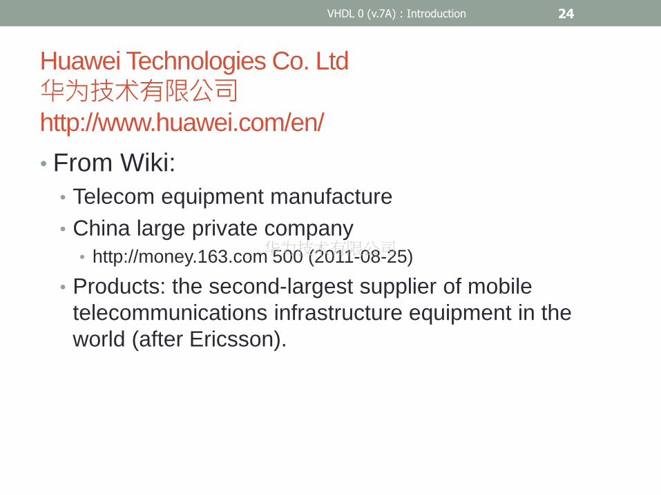
Huawei Technologies Co. Ltd
华为技术有限公司http://www.huawei.com/en/
• From Wiki:
• Telecom equipment manufacture
• China large private company
• http://money.163.com 500 (2011-08-25)
• Products: the second-largest supplier of mobile
telecommunications infrastructure equipment in the
world (after Ericsson).
VHDL 0 (v.7A) : Introduction 24
华为技术有限公司

References
• See course web page
• Digital Systems Design Using VHDL, Charles H. Roth
(first or second edition)
• Rapid Prototyping of Digital Systems, by Hamblen,
James etal. Springer 2008. (read_online)
• Digital Design: Principles and Practices, 4/E John F.
Wakerly, Prentice Hall.
• High-Speed Digital Design: A Handbook of Black
Magic by Howard W. Johnson and Martin Graham
Prentice Hall.
• BOOKBOON (Free text books)
• http://www.alldatasheet.com/
VHDL 0 (v.7A) : Introduction 25

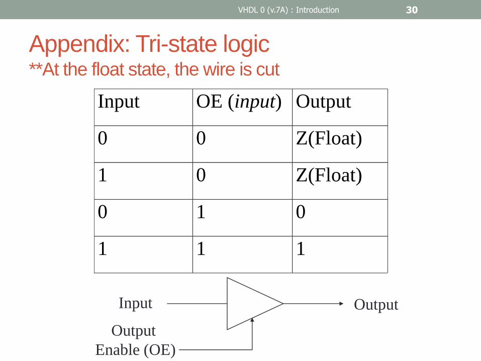
TRI-STATE LOGIC The concept of tri-state logic is essential in computer
design, so we want to revise these techniques before we
move on.
VHDL 0 (v.7A) : Introduction 29
VHDL 0 (v.7A) : Introduction 30
Input
Output
Enable (OE)
Output
Appendix: Tri-state logic**At the float state, the wire is cut
Input OE (input) Output
0 0 Z(Float)
1 0 Z(Float)
0 1 0
1 1 1

Tri-state equivalent circuit
(using output connect/cut view)
VHDL 0 (v.7A) : Introduction 31
Input
Output
Enable (OE)
Output
Input
Output
Enable (OE)
Output
OE=1, switch close
OE=0, switch open
Same as

Alternatively: We can treat the Tri-state equivalent
circuit using the Rout impedance view
VHDL 0 (v.7A) : Introduction 32
Input
Output
Enable (OE)
Input
Output
Enable (OE)
Output
When OE=1, Rout = small, (e.g. 50 Ω )
When OE=0, Rout = infinity (e.g. 10 MΩ)
Same as
Rout
OE (output enable) controls the value of Rout
Tri-state equivalent circuit :Rout impedance viewto explain the concept of tri-stat
A tri-state circuit diagram
Output

VHDL 0 (v.7A) : Introduction 33
Input
Output Enable (OE)
Output
5V10K
Input Output-Enable
OE (input) Output
0 0 ? ___
1 0 ? ___
0 1 ? ___
1 1 ? ___
**At float the wire is cut
A pull-up resistor is a resistor used to ensure a known state for a signal
Student ID: ___________,Date:_____________
Name: _______________
Exercise 0.1:Tri-state logic with pull up resistor

•
VHDL 0 (v.7A) : Introduction 34
Input1 Output-
Enable
OE
(input)
Output Equivalent Rout
(10M or 50)
Draw equivalent
circuit and find output
Voltage
0 0 ? _1__ ? ?
1 0 ? _1__ ? ?
0 1 ? _0__ ? ?
1 1 ? _1__ ? ?
Resistance view
Exercise 0.2: Use Rout (Impedance view) to explain the
result of exercise 0.1
Ohm’s Law
Hirchhoff Circuit Law:

Exercise 0.3 Application 1 of Tri-state logic:
Input/Output pin
• OE1 controls the traffic.
• Fill in the cells with ‘?’.
VHDL 0 (v.7A) : Introduction 35
Directional
control(OE1)
A
B
A Output
Enable
OE1 (input)
B
0 0 ?
1 0 ?
? 1 0
? 1 1

Exercise 0.4 Application 2 of Tri-state logic:
Transceivers for I/O data pins
• When T =1, A->B; T
controls the traffic,
• when /OE=1, IO pins
A,B are disabled
• Fill in the cells with ‘?’.
•
VHDL 0 (v.7A) : Introduction 36
A
B
/OE
T
T A Output
Enable
/OE1
(input)
B Which
controls
which
1 0 0 ? ?
0 1 0 ? ?
? ? 1 Float ?
? Float 1 ? ?
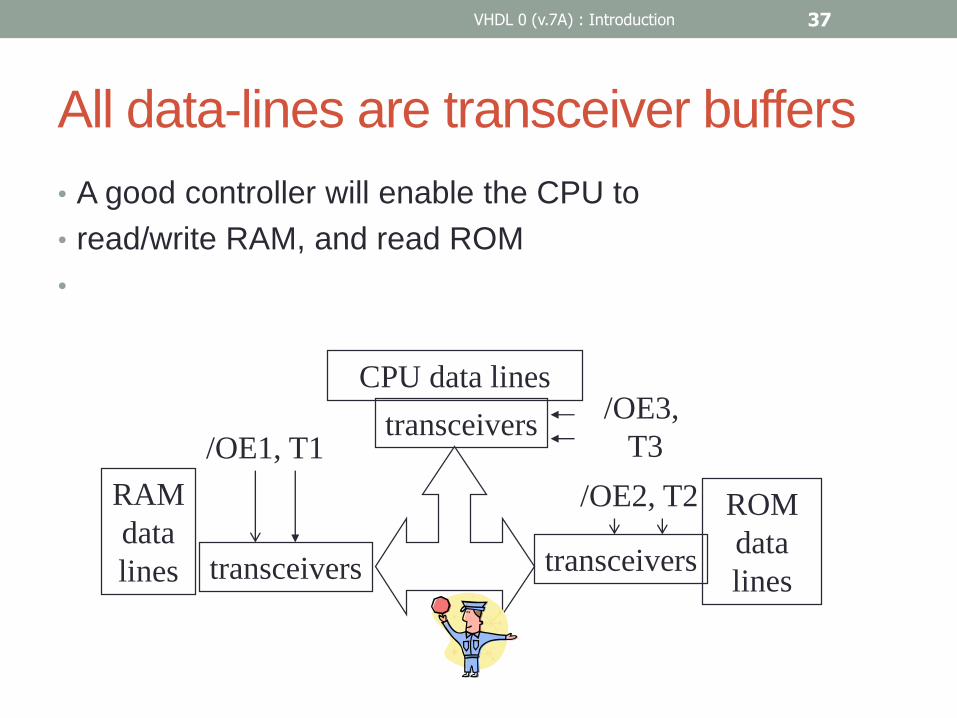
All data-lines are transceiver buffers
• A good controller will enable the CPU to
• read/write RAM, and read ROM
•
VHDL 0 (v.7A) : Introduction 37
CPU data lines
transceivers
ROM
data
lines
RAM
data
lines transceivers
transceivers/OE1, T1
/OE2, T2
/OE3,
T3

Exercise 0.5 :
List OE1,2,3 and T1,2,3 for the followings cases• a) CPU writes to RAM:
• /OE1=___ , /OE2___, /OE3=___, T1___, T2=____, T3_____
• b) CPU reads from ROM
• /OE1=___ , /OE2___, /OE3=___, T1___, T2=____, T3_____
• c) CPU reads from RAM
• /OE1=___ , /OE2___, /OE3=___, T1___, T2=____, T3_____
VHDL 0 (v.7A) : Introduction 38
CPU data lines
transceivers
ROM
data
lines
RAM
data
lines transceivers
transceivers/OE1, T1
/OE2, T2
/OE3,
T3
A
B
A B
B A

Exercise 0.6 Application 3 of Tri-state logic:
Selection of control signal (resolved logic)
• Output depends on Input_A if OE is _?___
• Output depends on Input_B if OE is _?___
• Discuss the operation of this circuit.
VHDL 0 (v.7A) : Introduction
39
Input_B
Input_AOutput
OE

Exercise 0.7
• Fill in ‘?’. Is it a “nor-gate” or an “or-gate”?
• Discuss the operation of this circuit.
• Answer :
VHDL 0 (v.7A) : Introduction 40
Output
OE2
5V
10K
OE10V
0V
Pull-up
Resistor OE1 OE2 Output
0 0 ?
1 0 ?
0 1 ?
1 1 ?