Embed Size (px)
Citation preview
Office of Research and Sponsored Programs
Office of Naval Research 875 N. Randolph Street Arlington, VA 22203-1995
Re : Grant# NOOO 14-15-1-2943
To Whom It May Concern:
April27 , 2017
Enclosed, please find the Final Technical Report and SF298 form for the grant referenced above.
Should you have any questions or need additional information, please feel free to contact me.
Sincerely,
Lori Gabriel Director
Cc: James Armistead Defense Technical Information Center~ ONR Patent Office Naval Research Laboratory ONR REG Office Atlanta
P.O . Box 7528 I Winston-Salem, NC 27109 I p 336.758.5888 I www.wfu .edu /rsp/

REPORT DOCUMENTATION PAGE Form Approved
OMB No. 0704-0188
The publ ic reporting burden for this collect ion of information is estimated to average 1 hour per response, including the time for reviewing instructions, searching existing data sources, gathering and maintaining the data needed , and completing and reviewing the collection of information. Send comments regarding this burden estimate or any other aspect of this collection of information, including suggestions for reducing the burden, to Department of Defense, Washington Headquarters Services, Directorate for Information Operations and Reports (0704-0188), 1215 Jefferson Davis Highway, Suite 1204, Arlington , VA 22202-4302. Respondents should be aware that notwithstanding any other provision of law, no person shall be subject to any penalty for failing to comply with a collection of information if it does not display a currently valid OMB control number. PLEASE DO NOT RETURN YOUR FORM TO THE ABOVE ADDRESS.
1. REPORT DATE (0 0 -MM-YYYY) 1 2. REPORT TYPE 3. DATES COVERED (From - To)
04/25/201 7 Final techn ica l report 09/01 /2015- 10/31 /2016 4. TITLE AND SUBTITLE Sa. CONTRACT NUMBER
Organic/Inorganic Hybrid Perovskite FETs for Electrically-Injected Laser Action
Sb. GRANT NUMBER
ONR N00014-15-1-2943 Sc. PROGRAM ELEMENT NUMBER
6. AUTHOR(S) Sd. PROJECT NUMBER
Oana D. Jurchescu (Co-PI Z. Valy Va rdeny, U Utah , under a different grant number)
Se. TASK NUMBER
Sf. WORK UNIT NUMBER
7. PERFORMING ORGANIZATION NAME(S) AND ADDRESS(ES) 8. PERFORMING ORGANIZATION
Wake Forest University REPORT NUMBER
Department of Physics 1834 Wake Forest Rd Winston-Salem, NC 27109 9. SPONSORING/MONITORING AGENCY NAME(S) AND ADDRESS(ES) 10. SPONSOR/MONITOR'S ACRONYM(S)
Office of Naval Research ONR
11. SPONSOR/MONITOR'S REPORT NUMBER(S)
12. DISTRIBUTION/AVAILABILITY STATEMENT
Approved for publ ic release: distribution unlimited .
13. SUPPLEMENTARY NOTES
14. ABSTRACT
Th is project will advance the development of the hybridorganic/inorganic hal ide perovskites (HOIHP by answering fundamental scientific questions with ramifications on potential applications of these materials. We will study the charge transport in HOIHP films and single crystals field-effect transistors (FETs); the magnetic-field-effect on current and electro-luminescence in these devices; and laser action aimed towards current injecting laser. For these studies we will use cw, transient and laser action techn iques on electrostatically gated devices.
1S. SUBJECT TERMS
16. SECURITY CLASSIFICATION OF: 17. LIMITATION OF 18. NUMBER
a. REPORT b. ABSTRACT c. THIS PAGE ABSTRACT OF PAGES
u u u uu I:Z
19a. NAME OF RESPONSIBLE PERSON
19b. TELEPHONE NUMBER (Include area code)
Standard Form 298 (Rev. 8/98) Prescribed by ANSI Std. Z39.18
Office of Naval Research (ONR)
Final grant report
_QNR N00014-15-1-2943
Organic/Inorganic Hybrid Perovskite FETs for
Electrically-Injected Laser Action
PI, Oana D. Jurchescu, Wake Forest University
In collaboration with Z. Valy Vardeny (University of Utah)
-supported under N00014-15-1-2524 ONR grant
Accomplishments
What were the major goals and objectives of the project?
Hybrid organic-inorganic solar cells based on the semiconductor methyl-ammonium (MA) lead
halide perovskites, MAPbX3 (where X=CI , Br, I) has recently and quite rapidly emerged as one of
the most promising contenders for larger scale photovoltaic energy generation . These materials,
while solution processed at low temperature, exhibit a remarkable set of materials properties
necessary for high efficiency thin film optoelectronic applications. This project aimed to advance
the development of the hybrid organic/ inorganic halide perovskites (HOIHP) by answering
fundamental scientific questions with ramifications on potential applications of these materials .
We had planned a set of experiments with the objectives to: (i) study the charge transport in HOIHP
films and single crystals in bulk and field-effect transistor (FETs) to advance the basic
understanding of charge transport in these materials , (ii) Improve the FET performance by tuning
the device design and processing, and (iii) Synthesize new Pb-free hybrid perovskites and
incorporate them in opto-electron ic applications.
What was accomplished towards achieving these goals?
Accomplishment 1: We lowered the trap densities in perovskite FETs and achieved high mobility and 'band-like' transport
Hybrid organic-inorganic halide perovskites were incorporated in a wide variety of devices
ranging from solar cells to light emitting diodes, lasers, spintronic devices and more. By careful
device design, we were able to fabricate the first working perovskite field-effect transistor (FET),
with support from this grant. 1 This device operated both in the p-type and n-type regime, with
typical charge carrier mobilities around I cm2/Vs at room temperature, in the dark, and reaching
mobilities as high as 10 cm2/Vs for several samples. The variations in electrical properties result
from charge trapping at the semiconductor/dielectric interface. Therefore, we further focused on
an in-depth study of the trap states by following the dependence of the carrier mobility on the
electric field , i.e. the Poole-Frenkel (PF) effect. We fabricated bottom-contact, top-gate FETs with
5 nm Til 50 nm Au source and drain electrodes treated with various self-assembled monolayers
(SAMs), Cytop gate dielectric and AI or Au top-gate electrode. Since one of the main sources for
the traps arises from the microstructure of the hybrid perovskite film , we tuned the processing
parameters (SAM treatment, method for perovskite deposition, solution concentration, type of
solvent, etc) to vary the quality of this layer. The following SAMs were used:
Pentafluorothiophenol (PFBT); 4-(trifluoromethyl)thiophenol (TFBT); and 2,3,5,6-tetrafluoro-4-
(trifluoromethyl) benzenethiol (TTFP). For comparison we also fabricated FETs with no
treatment.
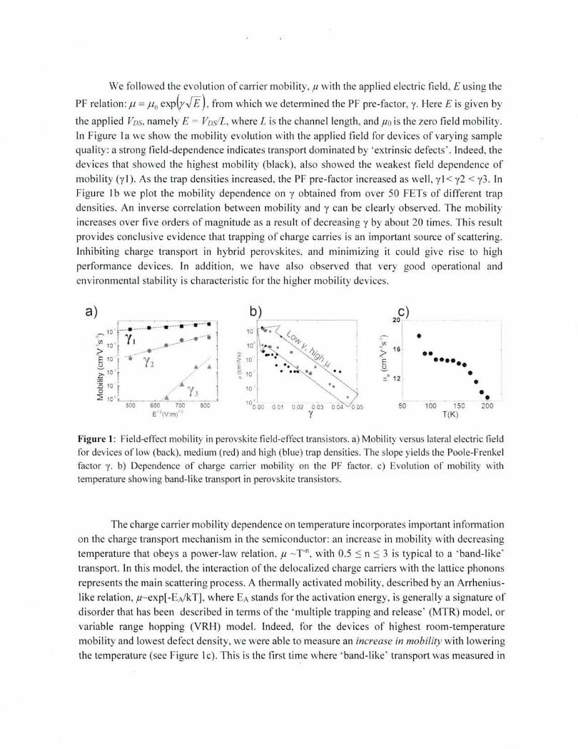
We followed the evolution of carrier mobi I ity, f1 with the applied electric field , E using the
PF relation: Jl =flo exp~JE), from which we determined the PF pre-factor, y. Here E is given by
the applied Vos, namely E = Vos/L, where Lis the channel length , and fl O is the zero fi eld mobility. In Figure I a we show the mobility evolution with the app lied field for dev ices of varying sample quality: a strong field-dependence indicates transport dominated by 'extr insic defects ' . Indeed, the devices that showed the highest mobility (bl ack), also showed the weakest field dependence of mobility (y I). As the trap densities increased, the PF pre-factor increased as we ll , y 1 < y2 < y3. In Figure I b we plot the mobility dependence on y obtained from over 50 FETs of different trap densities. An inverse correlation between mob ili ty and y can be clearly observed. The mobility increases over fi ve orders of magnitude as a result of decreasing y by about 20 times. Thi s result provides conclusive ev idence that trapping of charge carri es is an important source of scattering.
Inhibiting charge transpot1 in hybrid perovsk ites, and minimizing it could give rise to high performance devices . In add ition, we have al so observed that very good operational and enviro nmental stab ility is characteristic for the higher mobility devices.
a) 10 . t---· -----· -- --------· ----· ---·
:: - r· y. _____ ... ---~ -"' 10 ' · ----;;. ---------E 10 r --. ---- y / g I 2 ~/ • ~ 1o 'r //
:6 10 [ / &.y 0 f / 3 ~ 10 ' ' .•
500 600 700 800
E''(V/m) 'z
'" . ?; 10 E ~ 10
7
1Q I
10 ~ 00 0 0 1 0 02 0 03 y
• •• ••••••
• • • -~
50 100 150 200 T(K)
Figure 1: Field-effect mobility in perovskite fi eld-effect transistors. a) Mobility versus lateral electric field for dev ices of low (back), med ium (red) and hi gh (blue) trap densities. The slope yields the Poole-Frenkel factor y. b) Dependence of charge carrier mobility on the PF factor. c) Evolution of mobility with temperature showing band-like transport in perovskite transistors.
The charge carrier mobility dependence on temperature inco rporates impot1ant information on the charge transport mechanism in the semiconductor: an increase in mobility with decreas ing temperature that obeys a power-law relation, f1 - Tn, with 0.5 :S n :S 3 is typical to a ' band-like' transport. In thi s model, the interaction of the de localized charge carriers with the lattice phonons represents the main scattering process. A thermally activated mobility, described by an Arrheniuslike relation, 11- exp[-EA/kT] , where EA stands for the activation energy, is generally a signature of disorder that has been described in tenns of the ' multiple trapping and release ' (MTR) model, or
variable range hopping (VRH) model. Indeed, for the dev ices of highest room-temperature mobility and lowest defect density, we were able to measure an increase in mobility with lowering the temperature (see Figure l c). This is the first time where ' band-like' transport was measured in

hybrid perovskite transisto rs; it results from an aggressive lowering of the trap densities at the semiconductor/dielectric interface. This was achieved by carefully controlling the perovskite film microstructure, coupled with the use of an inert organic dielectric, and the use of SAMs to control the film order and charge injection.
Accomplishment 2: Transport studies using time-of-flight measurement
For studying carrier mobility, p of methyl-ammonium lead trihailde perovskites (MAPbXJ) using the time of flight (TOF) method, it is required to perform the measurements on a sample of thickness larger than can be generated through either solution-based or evaporation techniques. We succeeded in growing such single crystals of MAPbBr3, and more recently also MAPbb, with dimensions of l-4mm to obtain the large transport lengths, L necessary for TOF. Planar diode
structures have been fabricated by evaporating a semi-transparent (30nm) Au layer on one surface of the crystal as anode. Ag-epoxy is used as cathode and also as heat sink the crystal to the 'cryostat sample holder ' for temperature control during the measurements. This device architecture allows for .measurement of electron transpot1, as photo-excitation is through the electron-injectionblocking Au contact. These contacts are not ideal , and later work involved improvement of the diode structure that allowed for studying hole transport by replacing the Ag-epoxy with ETLIAI(30nm), where ETL is a few nm thin electron-transport-layer such as C6o.
a) 10'
-, .
-110\J -nov
10 ' -sov -70V
10 -
b) ,l
J' j" E , ~
\ I
10
.L -- T
I (LlS)
! •
----y---- .-------
50 100 150 200 250 300 Temperature fK)
c) ~
' E
.I " ~· . i ["-•- ro .. ·
Below-E :
12PAi •, ,, .. ·'\:
w I
w '1 j
Above [~ I . I 2 ~
: '--- · ~ -·- .
" ...
' .. I '
" " Ire d.om Photol'l Ene.•;JY toV)
d ) ~~ -5cm2Ns sx,o' ·~, .._ - 1.93eV
~ '\'\·~ - 2.10eV " ''\ '. . - 2.15cV ~ · .. \ ... 2 21 v ;; \~ " ,. -. e ~ 5x1o• ~ - 7cm2N s ~. o. -2.28eV
-233eV - 2.39cV - ? .48cV
10 15 20 25 30 35 40 t ( ~ s)
Figure 2. (a) Log-log plot of PC vs. time at different applied voltages for l mm thick MAPbBr3 crystal. The lines indicate asymptotes of the two power laws, the intersections of which (squares) are indicated by the vertical lines. Inset: The extracted trr in IJ.S v . IN. (b) Values of ~L extracted at different temperatures. (c) Percent of incident photons converted to electrons (EQE) vs. the excitation photon energy. The reddashed line indicates the lower bound of the optical band gap Eg. (d) PC transients for several different incident photon energies.
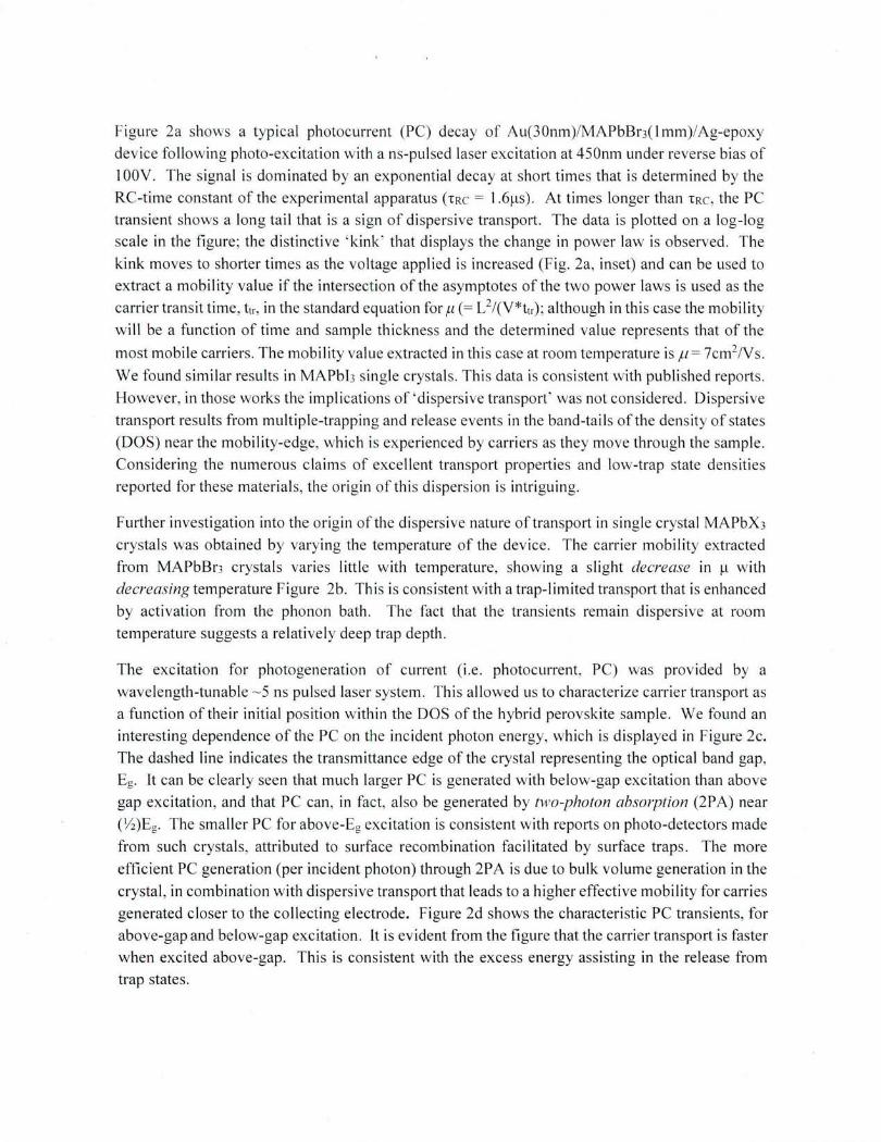
Figure 2a shows a typical photocurrent (PC) decay of Au(30nm)/MAPbBr3(lmm)/Ag-epoxy device following photo-excitation with a ns-pulsed laser excitation at 450nm under reverse bias of I OOV . The signal is dominated by an exponential decay at short times that is determined by the RC-time constant of the experimental apparatus (tRc = l.611s) . At times longer than tRc, the PC transient shows a long tail that is a sign of dispersive transport. The data is plotted on a log-log scale in the figure ; the distinctive ' kink ' that displays the change in power law is observed. The kink moves to shorter times as the voltage applied is increased (Fig. 2a, inset) and can be used to extract a mobility value if the intersection ofthe asymptotes of the two power laws is used as the carrier transit time, ttr, in the standard equation for f.1 (= L2/(V*ttr) ; although in this case the mobility wi II be a function of time and sample thickness and the determined value represents that of the
most mobile carriers. The mobility value extracted in this case at room temperature is 11 = 7cm2/Vs.
We found similar results in MAPbb single crystals. This data is consistent with published reports. However, in those works the implications of ' dispersive transport ' was not considered. Dispersive transport results from multiple-trapping and release events in the band-tails of the density of states (DOS) near the mobility-edge, which is experienced by carriers as they move through the sample. Considering the numerous claims of excellent transpott properties and low-trap state densities reported for these material s, the origin of thi s di spersion is intriguing.
Further investigation into the origin ofthe di spersive nature oftransport in single crystal MAPbX3 crystals was obtained by varying the temperature of the device . The carrier mobility extracted from MAPbBn crystals varies little with temperature, showing a slight decrease in ~t with decreasing temperature Figure 2b. This is consistent with a trap-limited transport that is enhanced by activation from the phonon bath. The fact that the transients remain dispersive at room temperature suggests a relatively deep trap depth.
The excitation for photogeneration of current (i .e. photocurrent, PC) was provided by a wavelength-tunable - 5 ns pulsed laser system. This allowed us to characterize carrier transport as a function of their initial position within the DOS ofthe hybrid perovskite sample. We found an interesting dependence of the PC on the incident photon energy, which is displayed in Figure 2c. The dashed line indicates the transmittance edge of the crystal representing the optical band gap, Eg. It can be clearly seen that much larger PC is generated with below-gap excitation than above gap excitation, and that PC can, in fact, also be generated by two-photon absorption (2PA) near
(Yz )Eg. The smaller PC for above-Eg excitation is consistent with reports on photo-detectors made from such crystals, attributed to surface recombination facilitated by surface traps. The more efficient PC generation (per incident photon) through 2PA is due to bulk volume generation in the
crystal , in combination with dispersive transport that leads to a higher effective mobility for carries generated closer to the collecting electrode. Figure 2d shows the characteristic PC transients, for above-gap and below-gap exc itation. It is evident from the figure that the carrier transport is faster when excited above-gap. This is consistent with the excess energy assisting in the release from trap states.

Accomplishment 3: Perovskite FET transistors on hydrophobic surfaces
Solution-processab le electronic dev ices are highly des irable due to their low cost and compat ibil ity with flex ible substrates . However, they are often chall enging to fabricate due to the hydrophobic nature of the surfaces of the constituent layers. To date, most of so lution-deposited dev ices had onl y one or a few layers depos ited from so lution, using simple methods such as inkjet printing, spin casting, or spray coating, whil e the other layers were obtained by electron-beam evaporation, thennal evaporation, or other complex technologies, which significantly increased the overall cost of fabrication and limited their applicability. This compromise was necessary, however, because the hydrophobic nature of many so lution-deposited compounds precluded the depos ition of consecutive layers onto their surface. In thi s project, we deve loped a method fo r tailoring the surface properties of the highl y hydro phobic di electric Cytop by applying a treatment with a
protein so lution to improve its wettability and allow fo r subsequent so lution process ing at its surface . We find that thi s treatment does not alter the electri cal properties of the Cytop layer, but increases its surface energy suffi cientl y to allow for so lution-deposition of other layers on its surface . We then fabricate bottom-gate FET devices on the protein/Cytop dielectric wi th halide perovskite semiconductors.
8x10"
6x10"
2x1 0"
' ~l 5 ,=004 Cr:1 V S
' LIW = 30/1000 C"'~ = 2.42 nF/cm
2
~L =0 23 cm'v 's sat
0
oooooooo
-1 5 -10
VGS 0/)
Figure 3. Drain cun·ent versus the appl ied gate-source voltage in the saturation regime, at roomtemperature, for a FET with protein/Cytop bottom gate. The device geometry and dielectric capacitance, as well as the perovskite structure are include in the inset.
A typical transfer curve is shown in Figure 3. The inset in thi s fi gure represents the crystal structure of the perovskite, with the Pb2
+ cations and the halide anions sitting at the centers and corners of
the octahedra, respecti ve ly; and the methylammonium organic cations in the interstices. The current-voltage characteri stics shown here deviates from a straight line necessary in order to use equati on (1) for mobili ty estimation. Thi s type of behav ior re ul ts from severe contact effects, which we have discussed in detail elsewhere.41 In the low-vo ltage regime we obtained ~ = 0.23 cm2V·1s· 1, a value which is most li kely an overestimation of the real mobility of thi s dev ice, while the value obtained at high vo ltages, ~ = 0.04 cm2V.1s. 1is a more conservative estimation. Both

values, however, are lower than the mobi lity obtained on the same perovskite layer, but w ith Cytop
top die lectr ic, 1-l = 1.3 cm2V-'s-1. This is probabl y due to increased density of trapping states at the
semiconductor/dielectric interface because ofthe insetii on ofthe protein layer. In addition, while
for the top-gate devices with neat Cytop dielectric laye r we observed ambipolar transport, we
found that the electron transport was inhibited at the hydrophilic interface created by the prote in
treatment.
Accomplishment 4: Large-area electron ics on hybrid perovskites
Impress ive demonstrati ons in the field of hybrid perovskite e lectronics have generated excitement
in studying these type of mater ial s. But, with a few exceptions, the properti es of devices reported
in the literature can onl y be reproduced over small areas . Achi ev ing good performance and
uniformity over large-areas is hard due to the lack of processing meth ods that maintains film
quality over large areas. Scaling up from laboratory-based dev ices to large-area e lectronics w ithout
compromis ing performance is one of the big challenges faced by the field . Because of this, we focused our efforts not only towards improving device pe1jormance, but also in ensuring that this
pe1jormance is recovered over large areas, without exorbitant fabrication costs. We employed
' spray-coat ing ' for the deposition of the hybrid perovskite layer. T hi s is a fast, high -throughput
manufacturing method that is easily scalable to large areas.
0 0030 ~~ • • • •
• I • \
----.. 0 0025
~
~00020 • •
• • 0 0 0015
V =-10V '-- .J os ~s=10V 0 0010
-30 -20 -10 0 10 20 30
V GS (V)
Figure 4 . Evo lution of the drain current versus the drain voltage in spray-depos ited perovskite field-effect transistors in the saturation regime for p-type (red) and n-type (blue) operation. The inset shows a photo of
the device.
To perform ' spray-coating' , we started with the Si/S iOz/Ti/Au substrates, simi lar to our spin
coating studies. The semiconductor was di sso lved in a solvent and the solution was directed toward
the substrate with an air brush he ld at a controlled di stance h above the substrate . The solution was
atomized by appl ying pressure to high-purity Ar, the transporting gas. We learned that fil m
formation by ' spray-coating ' method is cri t ica ll y affected by such process ing deta il s as so lution
concentration, type of so lvent (boiling point, vapor pressure , viscos ity) , spraying distance ,
transporting gas pressure, substrate temperature, and substrate surface energy. Consequentl y, we
systemati call y modifi ed these parameters to improve film morphology. Surface energy was also
modified using SAMs. We fo und that at reduced rates, obtained using a sma ll nozzle opening
and/or reduced A r pressure, femtoliter-s ized droplets landed on the surface fo rming domains that
dried independentl y without particularl y good interconnecti vity. At very large deposition rates, a
continuous wet layer formed . Therefore, by trial and error we determined the intermediate rates ,
which allowed us to obta in hi gh qua li ty film s.
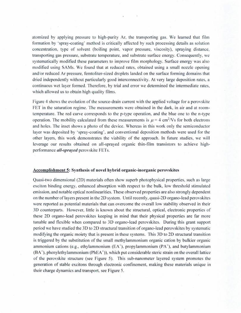
Figure 4 shows the evo lution of the source-dra in current w ith the applied vo ltage for a perovskite
FET in the saturati on regime. The measurements were obtained in the dark, in air and at room
temperature. The red curve corresponds to the p-type operati on and the blu~ one to the n-type
operati on. The mobility calculated from these mea urements is f.-l = 4 cm2/Vs fo r both electrons
and ho les . The inset shows a photo of the dev ice. Whereas in thi s work only the semiconductor
layer was depos ited by 'spray-coating ', and conventi onal depositi on method were used fo r the
other layers, thi s work demonstrates the viability of the approach . In future studies, we will
leverage our results obtained on all-sprayed o rgantc thin-film transistors to achi eve hi gh
perfo rmance all-sprayed perovskite FETs.
Accomplishment 5: Synthesis of novel hybrid organic-inorganic perovskites
Quas i-two dimensional (2D) materials often show superb photophys ical properties, such as large
exc iton binding energy, enhanced abso rption with respect to the bulk, low threshold stimulated
emiss ion, and notable opti cal nonlineariti es . These observeq properties are al so strongly dependent
on the number of layers present in the 20 system. Until recently, quas i-20 organa-lead perovskites
were reported as potentia l material s that can overcome the overall low stability observed in the ir
3D counterparts. However, littl e is known about the structural , optica l, electronic properties of
these 2D organa-lead perovskites keeping in mind that the ir phys ical properties are far more
tunabl e and fl ex ible when compared to 3D organa-lead perovskites. During thi s grant support
peri od we have studi ed the 30 to 20 structura l transition of organo-lead perovskites by systemati c
modify ing the organic mo iety that is present in the e systems. Thi s 30 to 2D structura l transition
is tri ggered by the substitution of the small methylammonium organic cation by bulkier organic
ammonium cations (e .g. , ethylammonium (EA +), propylammonium (PA +), and butylammonium
(BA +), phenylethy lammonium (Ph EA +)), which put considerable steric strain on the overall latti ce
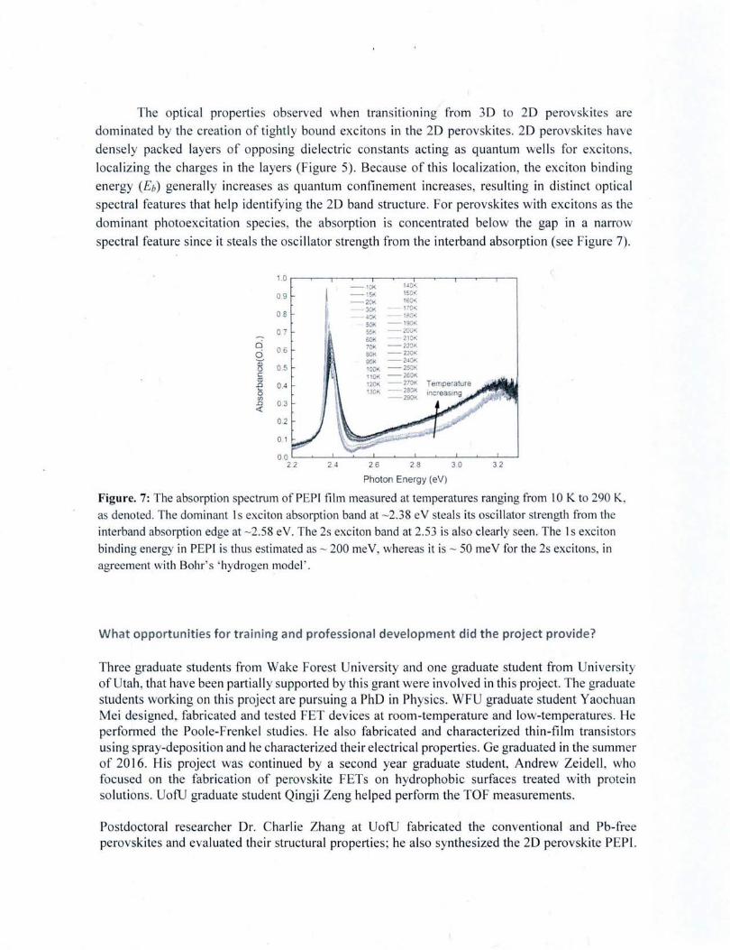
of the perovski te structure (see Figure 5) . This sub-nanometer layered system promotes the
generation of stable exc itons through electronic confinement, making these materi als unique in
the ir charge dynamics and transport, see Figure 5.

0 64 nm lnorganoc ,. ell
o: -6. E= 4 2 eV
lnm Orga nic barner t. =-2 3, E= 2.4 ev
• @ • @ • €- • @ • • •
Substra e
0 PtJ2•
• I CH.C, H, i ·
Figure 5: Schematic of the 20 organic-inorganic perovskite PEP I that shows naturally formed multiple quantu m well s compri sed of alternati ng layers of inorgan ic Pbl4- and organic barriers
Figure 6 depicts X-ray di ffraction (X RD) spectra of several perovskites thin fi lms with di ffere nt organic cations that were synthes ized at the Uni vers ity of Utah (UofU). These films were prepared by sp in-coating a so lution compri sed of J: I molar ratio of cation:Pb h fo r NH4 Pb b, MAPb b , and
EAPb b and 2: 1 molar rati o of cation:Pbh fo r perovskites (PA)2Pbf4, and (BA)2Pbl4, in dimethylformamide (DMF). The XRD spectra in Figure 6 show the fo rmation of low-dimensional laye red structures when the methylammonium cat ion is replaced with larger cations. These low dimensional structures were formed by slicing along the ( 11 0) face of the 3D perovskite in such a
way that the c-axis (00/) is the dominant phase of the 2D perovskite layers. Moreover, introducti on of a larger cation such as ethylammonium (EA +) within the PbiG inorganic cage shows the fo rmation of a highly ori ented system aligned along the (002) crystall ographic plane (F igure 6, brown line). The ali gnment along thi s plane suggests the fo rmation of a layered perovskite system.
Flllt hermore, as shown in Figure 6, the major c-ax is (002) crystall ographic plane shi fts to lower 28 va lues thus, suggesting a larger d-spacing as the perovski tes transition to a layered structure. We believe the observed latt ice expansion is due to the introduction of stronger van der Waals interactions within the larger cations and the inorganic cage .
.. !!. !!. (Ph EA )
2Pbl,
1 " • '" ~ 0 ......... 0
!!. (BA )2Pbl, - !!. :J
ro 0 • ;; .. ._... 0
2:: (PA), P b l, N
·u; 0 c Q) EAPbl 3 c
S'
MAP bl3
28 Figure 6. XRD patterns of vari ous perovskites structures that are based on different organi c cations. All diffraction peaks are indexed according to previous li terature values.
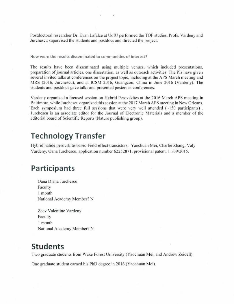
The optical properties observed when trans1t1oning from 3D to 20 perovskite are dominated by the creation of tightly bound excitons in the 20 perovskites. 20 perovskites have dense ly packed layers of opposing dielectric constants acting as quantum wells for excitons, localizing the charges in the layers (Figure 5). Because of this localization, the exciton binding energy (Eb) generally increases as quantum confinement increases, resulting in distinct optical spectral features that help identifying the 20 band structure. For perovskites with excitons as the dominant photoexcitation species, the absorption is concentrated below the gap in a narrow spectral feature since it steals the oscillator strength from the interband absorption (see Figure 7).
1.0
09
08
07
ci 06 ci
Q) 0.5 u
c ro .0 0'.4 0 (J)
.0 <(
03
02
0.1
0.0 22 24
-10K -15K - 2CK - JCK
•cK SCK 55K 60K 70K SCK 90K 100K 110K
140K 150K 160K 170~
- 180K -190K -200K - 210K -220K -230K -240K -250K -260K
120K -270K 130K - 280K
-290K
26 28
Photon Energy (eV)
30 3 2
Figure. 7: The absorption spectrum of PEPI film measured at temperatures ranging from I 0 K to 290 K, as denoted. The dominant Is exciton absorption band at - 2.38 eV steals its oscillator strength from the interband absorption edge at - 2.58 eV. The 2s exciton band at 2.53 is also clearly seen. The Is exciton binding energy in PEPI is thus estimated as - 200 meV, whereas it is - 50 meV for the 2s excitons, in agreement with Bohr's ' hydrogen model ' .
What opportunities for trai ning and professional development did the project provide?
Three graduate students from Wake Forest University and one graduate student from University of Utah, that have been partially supported by this grant were involved in thi s project. The graduate students working on this project are pursuing a PhD in Physics . WFU graduate student Yaochuan Mei designed ,. fabricated and tested FET devices at room-temperature and low-temperatures. He performed the Poole-Frenkel studies. He also fabricated and characterized thin-film transistors using spray-deposition and he characterized their electrical properties. Ge graduated in the summer of 2016. His project was continued by a second year graduate student, Andrew Zeidell , who focused on the fabrication of perovskite PETs on hydrophobic surfaces treated with protein solutions. UofU graduate student Qingji Zeng helped perform the TOF measurements.
Postdoctoral researcher Dr. Charlie Zhang at UofU fabricated the conventional and Pb-free perovskites and evaluated their structural properties; he also synthesized the 20 perovskite PEPL
Postdoctoral researcher Dr. Evan Lafalce at UofU performed the TOF studies. Profs. Vardeny and Jurchescu supervised the students and postdocs and directed the project.
How were the results disseminated to communities of interest?
The results have been disseminated using multiple venues, which included presentations, preparation of journal articles, one dissertation , as well as outreach activities. The Pis have given several invited talks at conferences on the project topic, including at the APS March meeting and MRS (20 16, Jurchescu), and at LCSM 2016, Guangzou, China in June 2016 (Yardeny) . The students and postdocs gave talks and presented posters at conferences.
Yardeny organized a focused session on Hybrid Perovskites at the 2016 March APS meeting in Baltimore, while Jurchescu organized this sess ion at the 2017 March APS meeting in New Orleans.
· Each symposium had three full sessions that were very well attended (- 150 participants) . Jurchescu is an associate editor for the Journal of Electronic Materials and a member of the editorial board of Scientific Reports (Nature publishing group).
Technology Transfer Hybrid halide perovskite-based Field-effect transistors, Yaochuan Mei , Charlie Zhang, Yal y Vardeny, Oana J urchescu, application number 62252871, provisional patent, II /09/2015.
Participants
Oana Diana Jurchescu Faculty I month National Academy Member? N
Zeev Valentine Vardeny Faculty
I month National Academy Member? N
Students Two graduate students from Wake Forest University (Yaochuan Mei, and Andrew Zeidell).
One graduate student earned his PhD degree in 2016 (Yaochuan Mei).
One physics graduate student from the University of Utah (Qingji Zeng).
Publications
Y. Mei, C. Zhang, Z.V. Vardeny and 0.0. Jurchescu, Electrostatic gating of hybrid halide
perovskite field-effect transistors: balanced am bipolar transport at room-temperature, MRS
Commun 5, 297 ( 2015).
J. W. Ward, H. L. Smith, A. Zeidell , P. J. Diemer, S. R. Baker, H. Lee, M. M. Payne, J. E.
Anthony, M. Guthold, and 0.0. Jurchescu, Solution-Processed Organic and Halide Perovskite Transistors on Hydrophobic Surfaces, ACS Applied Materials & Interfaces, in revisions
E. Lafalce, C. Zhang, X. Liu, and Z. V. Vardeny, On the role of intrinsic ions accumulation in the photocurrent and photo-capacitive responses of MAPbBr3 photodetectors, ACS Applied
Materials and Interfaces, December 2016; I 0. 1 0211acsami .6b 11 925 .