Embed Size (px)
Citation preview
NotesA. Performance and quality attributes and conditions not expressly stated in this specification document are intended to be excluded and do not form a part of this specification document. B. Electrical specifications and performance data contained in this specification document are based on Mini-Circuit’s applicable established test performance criteria and measurement instructions. C. The parts covered by this specification document are subject to Mini-Circuits standard limited warranty and terms and conditions (collectively, “Standard Terms”); Purchasers of this part are entitled to the rights and benefits contained therein. For a full statement of the Standard Terms and the exclusive rights and remedies thereunder, please visit Mini-Circuits’ website at www.minicircuits.com/MCLStore/terms.jsp
Mini-Circuits®
www.minicircuits.com P.O. Box 350166, Brooklyn, NY 11235-0003 (718) 934-4500 [email protected]
50Ω 4500 to 6000 MHz 1:4 Ratio
RF Transformer NCS4-63+
Maximum RatingsOperating Temperature -40°C to 85°C
Storage Temperature -55°C to 100°C
Input RF Power*** 3W
Electrical Specifications (TAMB=25°C)
REV. CM172731NCS4-63+ED 12817/34B32RS/AM190219
Typical Performance Data at 25ºC**
Features• wideband, 4500 to 6000 MHz• low phase unbalance, 5 deg. and amplitude unbalance, 0.3 dB typ.• miniature size, 0.079”x0.049”x0.033”• LTCC construction• low cost• aqueous washable
Applications• WLAN• WIMAX• 802.11• radar
Ceramic Balun
ΩRATIO
(Secondary/Primary)
FREQUENCY(MHz)
INSERTION*LOSS(dB)
PHASE UNBALANCE AT
SECONDARY†
(Deg.)Typ.
AMPLITUDE UNBALANCE
(dB)
Typ.
4 4500-6000 1.0 5 0.5
FREQUENCY(MHz)
INSERTIONLOSS*(dB)
INPUTR. LOSS
(dB)
AMPLITUDEUNBALANCE
(dB)
PHASEUNBALANCE
(Deg.)
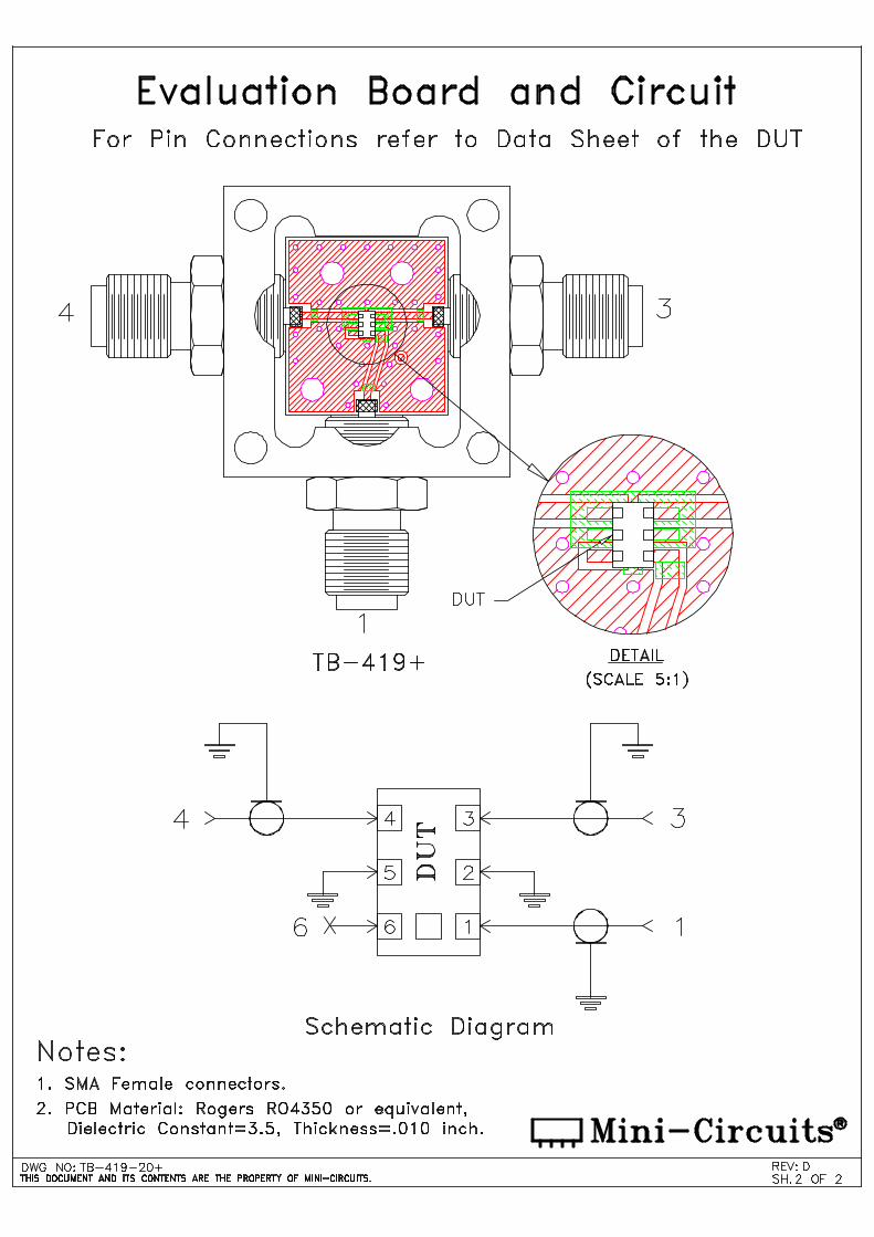
* Insertion Loss is referenced to mid-band loss, 0.7 dB. Reference Demo Board TB-419+† Relative to 180°
NCS4-63+INSERTION LOSS*
0.0
0.1
0.2
0.3
0.4
0.5
0.6
4500 4800 5100 5400 5700 6000FREQUENCY (MHz)
INS
ER
TIO
N L
OS
S (d
B)
NCS4-63+AMPLITUDE UNBALANCE
0.0
0.2
0.4
0.6
0.8
1.0
4500 4800 5100 5400 5700 6000FREQUENCY (MHz)
AM
PLI
TUD
E U
NB
ALA
NC
E
(dB
)
NCS4-63+PHASE UNBALANCE
0.0
2.0
4.0
6.0
8.0
10.0
12.0
4500 4800 5100 5400 5700 6000FREQUENCY (MHz)
PH
AS
E U
NB
ALA
NC
E (D
eg) configuration J
** Measured with Agilent E5071B network analyzer using impedance conversion and port extension.
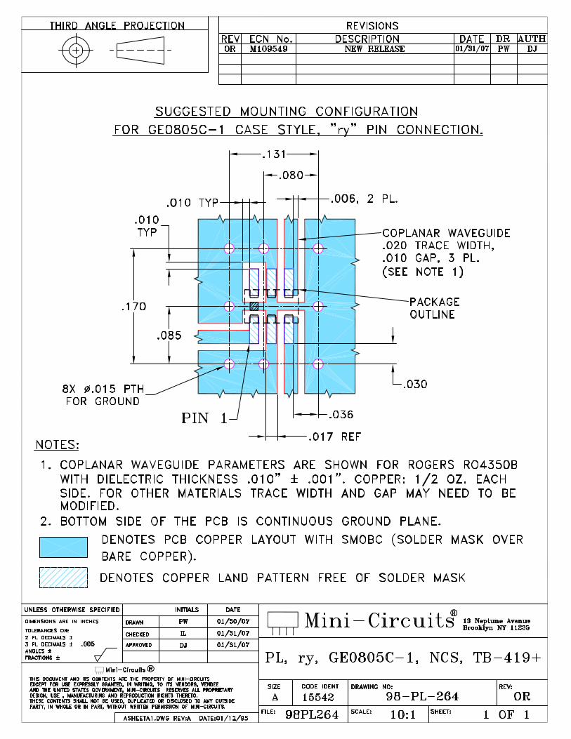
Demo Board MCL P/N: TB-419+Suggested PCB Layout (PL-264)
4500.00 0.09 14.03 0.04 8.50 4600.00 0.07 14.78 0.02 8.30 4900.00 0.02 16.64 0.02 5.52 5000.00 0.01 17.28 0.03 4.60 5200.00 0.00 18.16 0.18 2.85 5400.00 0.02 19.21 0.32 2.16 5600.00 0.06 19.53 0.30 1.25 5700.00 0.09 19.66 0.30 1.17 5800.00 0.12 19.00 0.22 0.35 6000.00 0.17 17.62 0.17 1.13
Pad ConnectionsPRIMARY DOT (Unbalanced Port) 1
PRIMARY (GND) 2,5
SECONDARY DOT (Balanced) 4
SECONDARY (Balanced) 3
NO CONNECTION 6Pads 2,3,4,5 are DC-connected internally
*** Derate linearly to 2W at 85°C Permanent damage may occur if any of these limits are exceeded.
Outline Drawing
A B C D E F.079 .049 .033 .014 .012 .0122.01 1.24 0.84 0.36 0.30 0.30
G H J K wt.026 .014 .039 .110 grams0.66 0.36 1.00 2.80 .008
Outline Dimensions ( )inchmm
Suggested L ayout, T olerance to be within ±.002
INDEX AREA*
*Shape of index marking may vary
PCB Land Pattern
NOCONNECTION*
PRI
SEC*Internal open circuit
CASE STYLE: GE0805C-1
Available Tape and Reel
at no extra cost
Reel Size Devices/Reel 7” 20, 50, 100, 200, 500,1000, 4000
+RoHS CompliantThe +Suffix identifies RoHS Compliance. See our web site for RoHS Compliance methodologies and qualifications

RF Transformer NCS4-63+Typical Performance Data
(MHz) (dB) (dB) (dB) (deg)
3000 3.95 2.88 1.40 5.953200 2.76 3.87 1.02 7.023400 1.85 5.10 0.67 7.473600 1.22 6.50 0.40 7.663800 0.76 8.14 0.22 7.814000 0.46 9.94 0.16 8.184100 0.35 10.85 0.17 8.154200 0.25 11.74 0.16 8.284300 0.18 12.57 0.12 8.524400 0.14 13.29 0.06 8.744500 0.10 14.03 0.04 8.504550 0.08 14.44 0.00 8.254600 0.08 14.78 0.02 8.304650 0.06 15.12 0.04 7.734700 0.06 15.47 0.04 7.504750 0.04 15.70 0.06 7.014800 0.04 16.06 0.06 6.634850 0.04 16.27 0.06 6.214900 0.03 16.64 0.02 5.524950 0.03 16.80 0.04 5.325000 0.02 17.28 0.03 4.605050 0.02 17.46 0.05 4.225100 0.02 17.72 0.12 3.285150 0.01 18.03 0.10 3.205200 0.01 18.16 0.18 2.855250 0.00 18.71 0.20 2.955300 0.01 18.69 0.28 2.105350 0.01 19.09 0.28 2.225400 0.03 19.21 0.32 2.165450 0.02 19.37 0.35 1.605500 0.04 19.71 0.34 1.885550 0.04 19.60 0.40 1.465600 0.07 19.53 0.30 1.255650 0.06 19.60 0.35 1.705700 0.10 19.66 0.30 1.175750 0.09 19.41 0.34 0.885800 0.13 19.00 0.22 0.355850 0.13 18.92 0.27 0.395900 0.15 18.43 0.19 0.475950 0.16 18.21 0.21 0.716000 0.18 17.62 0.17 1.136100 0.20 16.93 0.17 2.356200 0.22 16.34 0.24 3.426400 0.21 15.21 0.47 5.676600 0.26 14.07 0.79 6.977000 0.63 11.50 1.23 6.747250 0.94 9.65 1.43 7.317500 1.25 8.11 1.79 8.947750 1.64 7.07 2.53 10.818000 2.21 6.11 3.46 10.88
* Insertion Loss is referenced to mid-band loss , 0.7 dB.**Phase Unbalance is relative to 180˚
PHASE UNBALANCE**FREQUENCY AMPLITUDE
UNBALANCE
AVERAGEINSERTION
LOSS*
INPUTRETURN
LOSS
REV. X1NCS4-63+
070528Page 1 of 1

RF Transformer NCS4-63+Typical Performance Curves
* Insertion Loss is referenced to mid-band loss , 0.7 dB.
**Phase Unbalance is relative to 180˚
Average Insertion Loss* 0.0
0.5
1.0
1.5
2.0
2.5
3.0
3.5
4.0
4.5
5.03000 3500 4000 4500 5000 5500 6000 6500 7000 7500 8000
Frequency (MHz)
Ave
rage
Inse
rtion
Los
s (d
B)
Input Return Loss 0
2
4
6
8
10
12
14
16
18
203000 3500 4000 4500 5000 5500 6000 6500 7000 7500 8000
Frequency (MHz)In
put R
etur
n Lo
ss (d
B)
Amplitude Unbalance
0.0
0.5
1.0
1.5
2.0
2.5
3.0
3.5
4.0
4.5
5.0
3000 3500 4000 4500 5000 5500 6000 6500 7000 7500 8000
Frequency (MHz)
Am
plitu
de U
nbal
ance
(dB
)
Phase Unbalance**
0
2
4
6
8
10
12
14
16
18
20
3000 3500 4000 4500 5000 5500 6000 6500 7000 7500 8000
Frequency (MHz)
Pha
se U
nbal
ance
(deg
)
REV. X1NCS4-63+
070528Page 1 of 1
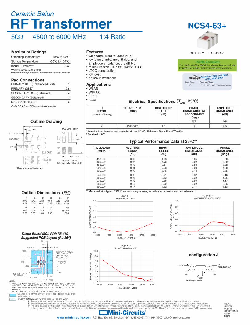
98-GE Rev.: Q (03/30/18) M167078 File: 98-GE.docx Sheet 2 of 14
This document and its contents are the property of Mini-Circuits.
Case Style GE
CASE # A B C D E F G H J K WT. GRAM
GE0805C-1 .079
(2.00)
.049
(1.25)
.033
(0.84)
.014
(0.35)
.012
(0.30)
.012
(0.30)
.026
(0.65)
.014
(0.35)
.039
(1.00)
.110
(2.80) .008
Dimensions are in inches (mm). Tolerances: 2Pl. + .01; 3 Pl. + .005
Notes: 1. Open style, ceramic base.
2. Termination finish: For RoHS Case Styles: Tin plate over Nickel plate. All models, (+) suffix.
For RoHS-5 Case Style: Tin-lead plate. All models, no (+) suffix.
PCB Land Pattern
Suggested Layout,
Tolerance to be within ±.002
Outline Dimensions
GE0805C-1
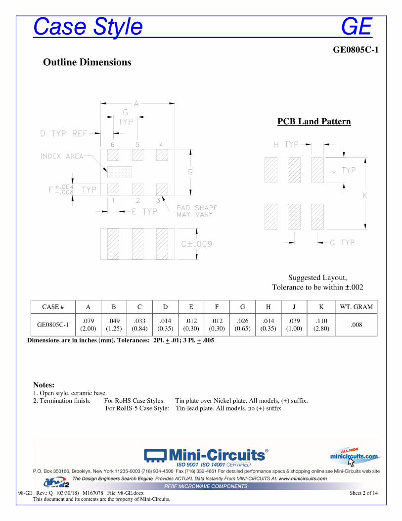
98-TR-F74 Rev.: K (05 JUL 21) ECO-008400 File:98-TR-F74 Sheet 1 of 1 This document and its contents are the property of Mini-Circuits.
Tape & Reel Packaging TR-F74
DEVICE ORIENTATION IN T&R
Tape Width, mm
Device Cavity Pitch, mm
Real Size, inches Devices per Reel
8 4 7
Small quantity standards (see note)
20 50
100 200 500
1000
Standard 2000 4000
Note: Small reel availability varies by model. Refer to pricing and availability on individual model dashboard. Mini-Circuits carrier tape materials provide protection from ESD (Electro-Static Discharge) during handling and transportation. Tapes are static dissipative and comply with industry standards EIA-481/EIA-541. Go to: www.minicircuits.com/pages/pdfs/tape.pdf
Applicable Case Styles GE0805C-1 GE0805C-1AP JV1210C-1 GU2939
Applicable Case Styles JV1210C JV1210C-2 JV1210C-3 JV1210C-4 JV1210C-5 JV1210C-6 JV1210C-11
Applicable Case Styles JC0603C-8 JV1210C-7 JV1210C-8 JV1210C-9 JV1210C-10 GE0805C-13
ILLUSTRATION 1
ILLUSTRATION 2
ILLUSTRATION 3
Mini-CircuitsEnvironmental Specifications
All Mini-Circuits products are manufactured under exacting quality assurance and control standards, and are capable of meeting published specifications after being subjected to any or all of the following physical and environmental test.
Specification Test/Inspection Condition Reference/Spec
ENV06T2
Operating Temperature -40° to 85° CAmbient Environment
Individual Model Data Sheet
Storage Temperature -55° to 100° CAmbient Environment
Individual Model Data Sheet
Humidity 90 to 95% RH, 240 hours, 50°C MIL-STD-202, Method 103, Condition A, Except 50°C and end-point electrical test done within 12 hours
Thermal Shock -55° to 100°C, 100 cycles MIL-STD-202, Method 107, Condition A-3, except +100°C
Solder Reflow Heat Sn-Pb Eutetic Process: 225°C peakPb-Free Process 245° - 250°C peak
J-STD-020, Table 4-1, 4-2 and 5-2, Figure 5-1
Solderability 10X Magnification J-STD-002, Para 4.2.5, Test S, 95% Coverage
Vibration (High Frequency) 20g peak, 10-2000 Hz, 12 times in each of three perpendicular directions (total 36)
MIL-STD-202, Method 204, Condition D
Mechanical Shock 50g, 11 ms, 1/2-sine, 18 shocks: 3 each direction, each of 3 axes
MIL-STD-202, Method 213, Condition A
This document and its contents are the property of Mini-Circuits.
Rev:ENV06T2 A 02/25/11 File:M130240 ENV06T2.pdf
Page: 1