Embed Size (px)
Citation preview
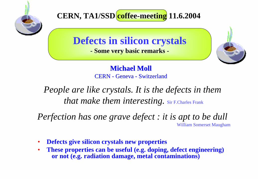
Defects in silicon crystals- Some very basic remarks -
Michael MollMichael MollCERN CERN -- Geneva Geneva -- SwitzerlandSwitzerland
CERN, TA1/SSD coffee-meeting 11.6.2004
People are like crystals. It is the defects in themthat make them interesting. Sir F.Charles Frank
Perfection has one grave defect : it is apt to be dullWilliam Somerset Maugham
• Defects give silicon crystals new properties• These properties can be useful (e.g. doping, defect engineering)
or not (e.g. radiation damage, metal contaminations)
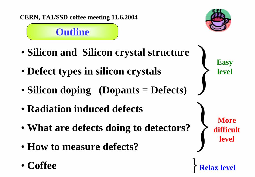
Outline
CERN, TA1/SSD coffee meeting 11.6.2004
• Silicon and Silicon crystal structure
• Defect types in silicon crystals
• Silicon doping (Dopants = Defects)
• Radiation induced defects
• What are defects doing to detectors?
• How to measure defects?
• Coffee
Easylevel
Moredifficult
level
Relax level}
Michael Moll – TA1/SD meeting – June 2004 -3-
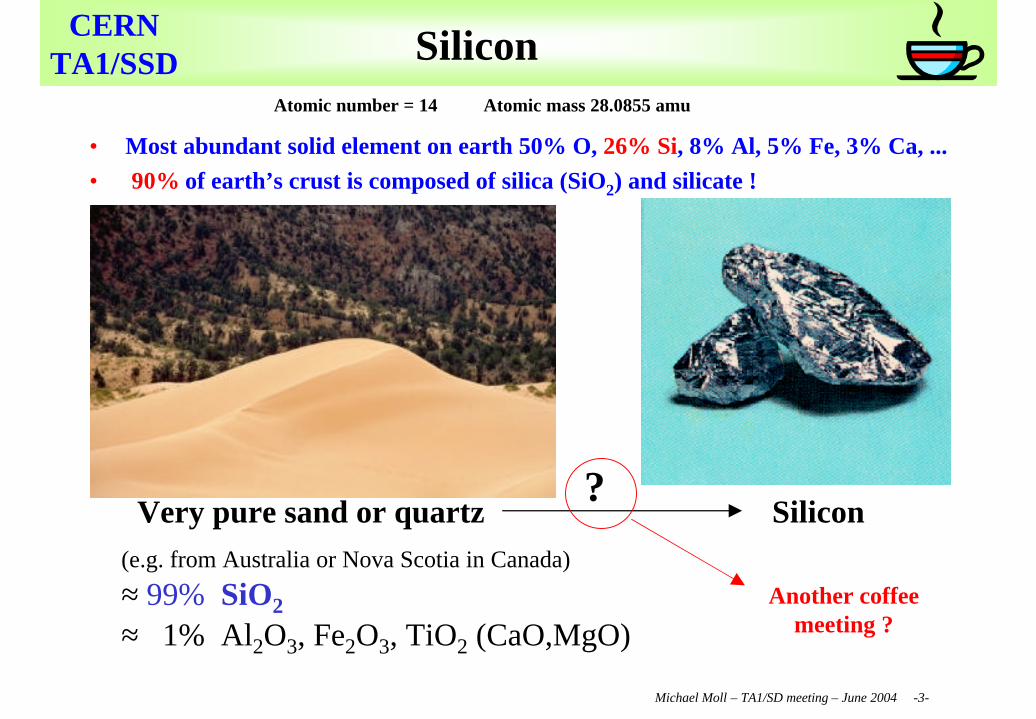
CERNTA1/SSD Silicon
• Most abundant solid element on earth 50% O, 26% Si, 8% Al, 5% Fe, 3% Ca, ... • 90% of earth’s crust is composed of silica (SiO2) and silicate !
Very pure sand or quartz Silicon(e.g. from Australia or Nova Scotia in Canada)
≈ 99% SiO2
≈ 1% Al2O3, Fe2O3, TiO2 (CaO,MgO)
Atomic number = 14 Atomic mass 28.0855 amu
?
Another coffee meeting ?
Michael Moll – TA1/SD meeting – June 2004 -4-
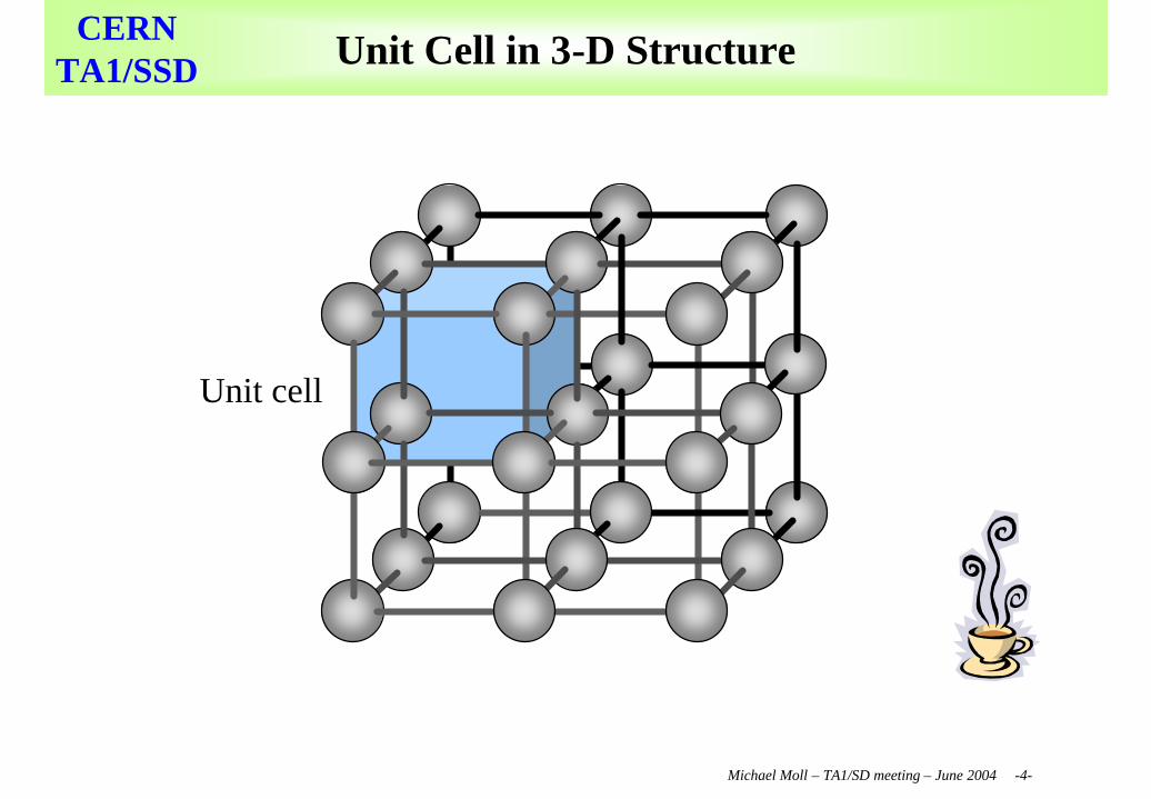
CERNTA1/SSD Unit Cell in 3-D Structure
Unit cell
Michael Moll – TA1/SD meeting – June 2004 -5-
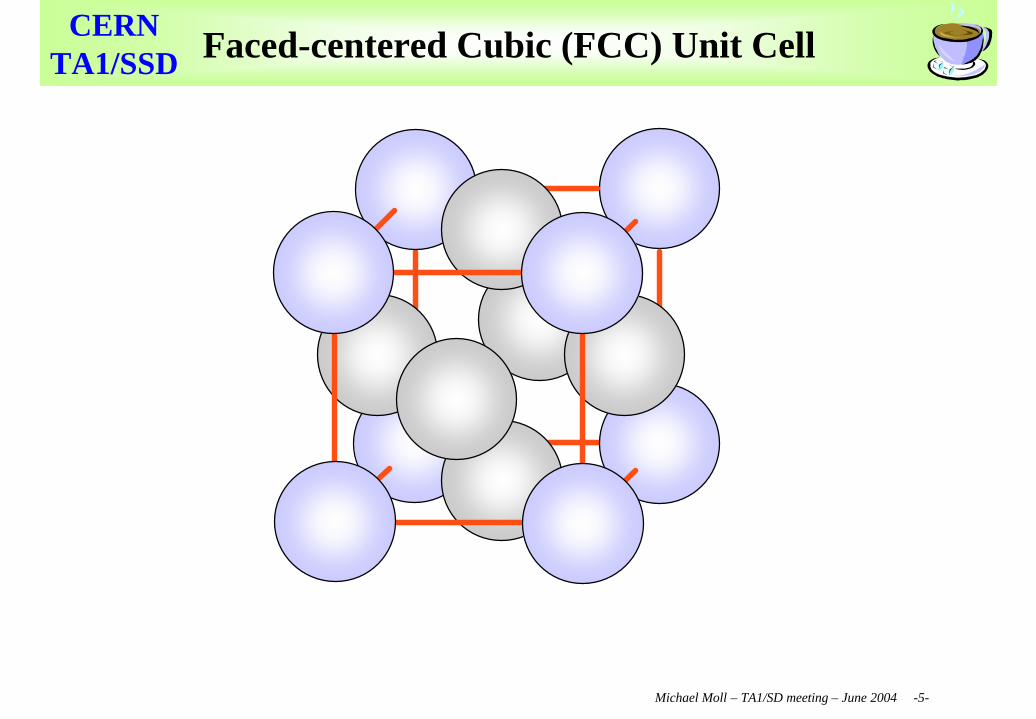
CERNTA1/SSD Faced-centered Cubic (FCC) Unit Cell
Michael Moll – TA1/SD meeting – June 2004 -6-
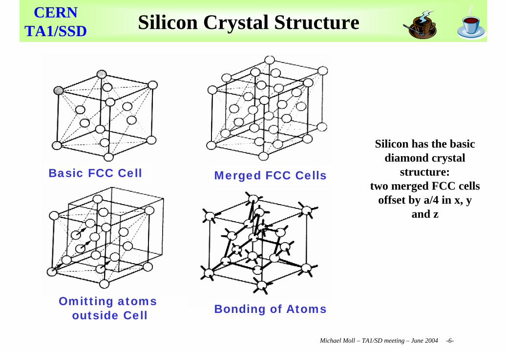
CERNTA1/SSD
Basic FCC Cell Merged FCC Cells
Omitting atomsoutside Cell Bonding of Atoms
Silicon Crystal Structure
Silicon has the basic diamond crystal
structure:two merged FCC cells
offset by a/4 in x, y and z
Michael Moll – TA1/SD meeting – June 2004 -7-
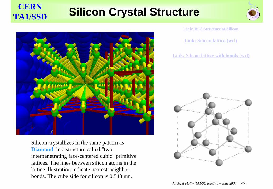
CERNTA1/SSD Silicon Crystal Structure
Silicon crystallizes in the same pattern as Diamond, in a structure called "two interpenetrating face-centered cubic" primitive lattices. The lines between silicon atoms in the lattice illustration indicate nearest-neighbor bonds. The cube side for silicon is 0.543 nm.
Link: BC8 Structure of Silicon
Link: Silicon lattice (wrl)
Link: Silicon lattice with bonds (wrl)
Outline
CERN, TA1/SSD coffee meeting 11.6.2004
• Silicon and Silicon crystal structure
• Defect types in silicon crystals•Lattice defects (Dislocations)
•Point defects (e.g. Impurities)
•Cluster defects and Precipitates
• Silicon doping (Dopants = Defects)
• Radiation induced defects
• What are defects doing to detectors?
• How to measure defects?
• Coffee
Michael Moll – TA1/SD meeting – June 2004 -9-
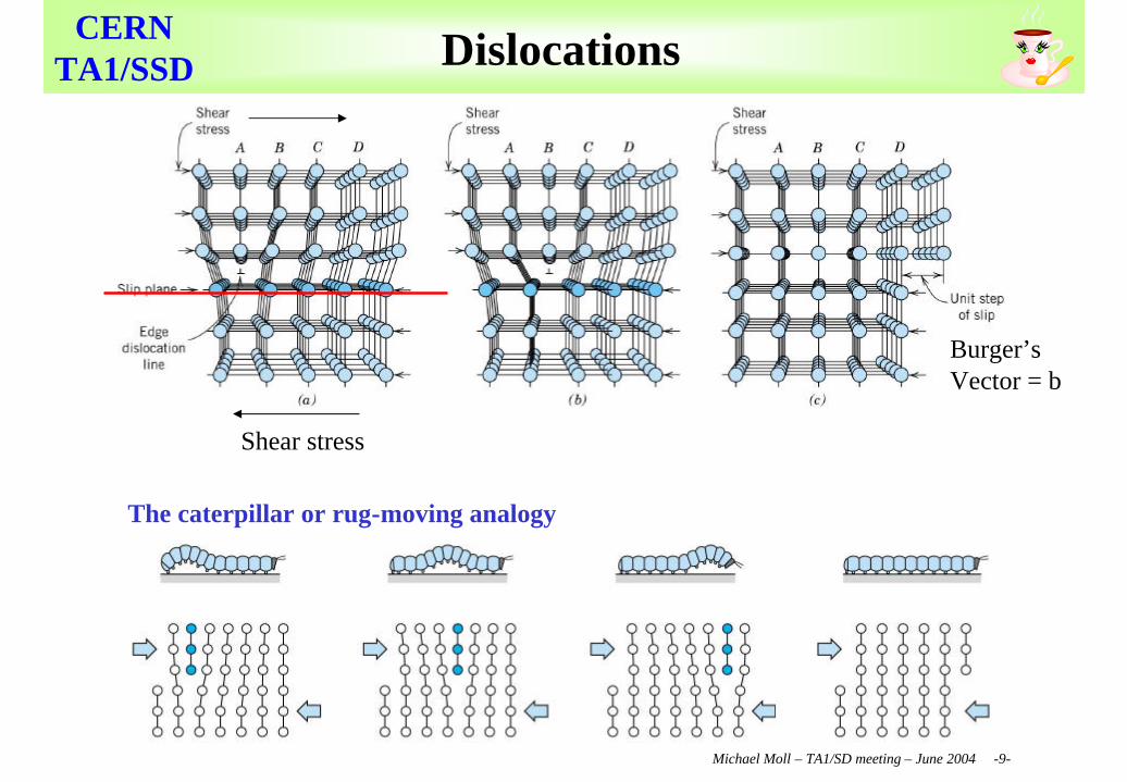
CERNTA1/SSD Dislocations
Shear stress
Burger’sVector = b
The caterpillar or rug-moving analogy
Michael Moll – TA1/SD meeting – June 2004 -10-
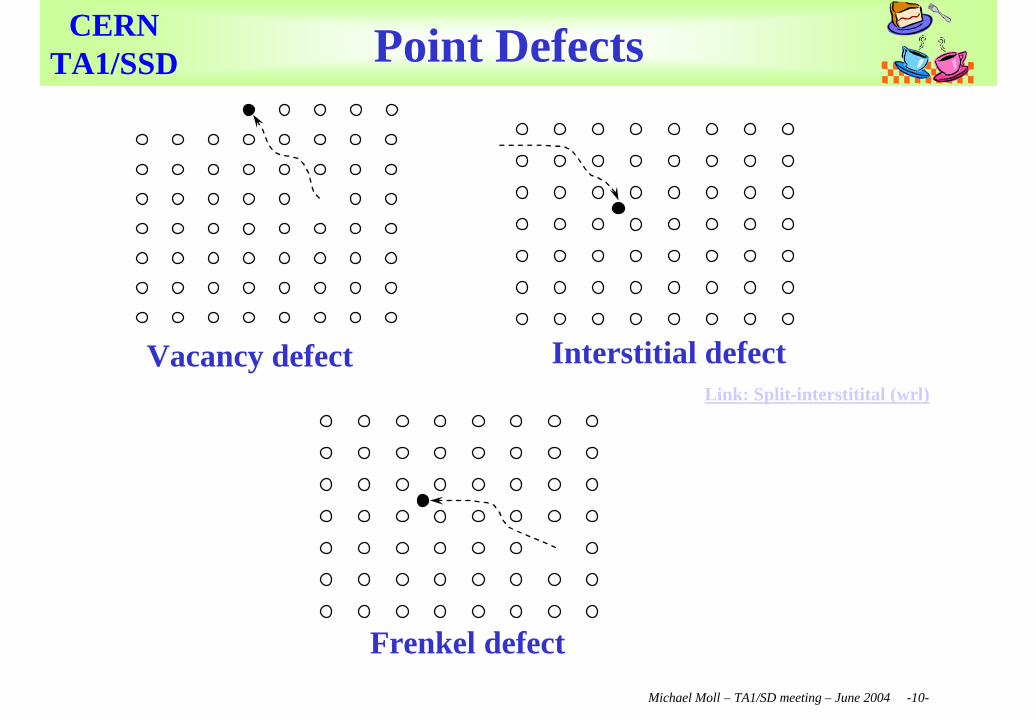
CERNTA1/SSD Point Defects
Vacancy defect Interstitial defect
Frenkel defect
Link: Split-interstitital (wrl)
Michael Moll – TA1/SD meeting – June 2004 -11-
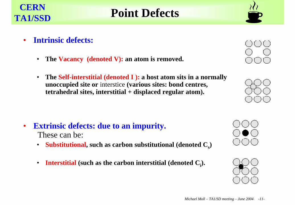
CERNTA1/SSD Point Defects
• Intrinsic defects:
• The Vacancy (denoted V): an atom is removed.
• The Self-interstitial (denoted I ): a host atom sits in a normally unoccupied site or interstice (various sites: bond centres, tetrahedral sites, interstitial + displaced regular atom).
• Extrinsic defects: due to an impurity. These can be:• Substitutional, such as carbon substitutional (denoted Cs)
• Interstitial (such as the carbon interstitial (denoted Ci).
Michael Moll – TA1/SD meeting – June 2004 -12-
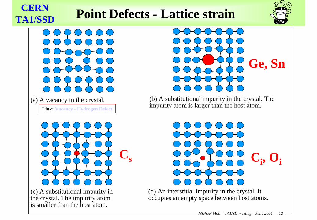
CERNTA1/SSD Point Defects - Lattice strain
(a) A vacancy in the crystal. (b) A substitutional impurity in the crystal. Theimpurity atom is larger than the host atom.
(c) A substitutional impurity inthe crystal. The impurity atomis smaller than the host atom.
(d) An interstitial impurity in the crystal. Itoccupies an empty space between host atoms.
Ge, Sn
Cs Ci, Oi
Link: Vacancy - Hydrogen Defect
Outline
CERN, TA1/SSD coffee meeting 11.6.2004
• Silicon and Silicon crystal structure
• Defect types in silicon crystals
• Silicon doping (Dopants = Defects)• Intrinsic silicon
• n-type silicon
• p-type silicon
• Radiation induced defects
• What are defects doing to detectors?
• How to measure defects?
• Coffee
Michael Moll – TA1/SD meeting – June 2004 -14-
CERNTA1/SSD
Si
Si SiSi
Si
Si
Si Si
Si Si
Si
Si
Si
Si
Si
Si
Si
Si Si
Si Si
Si
Si
Si
Si
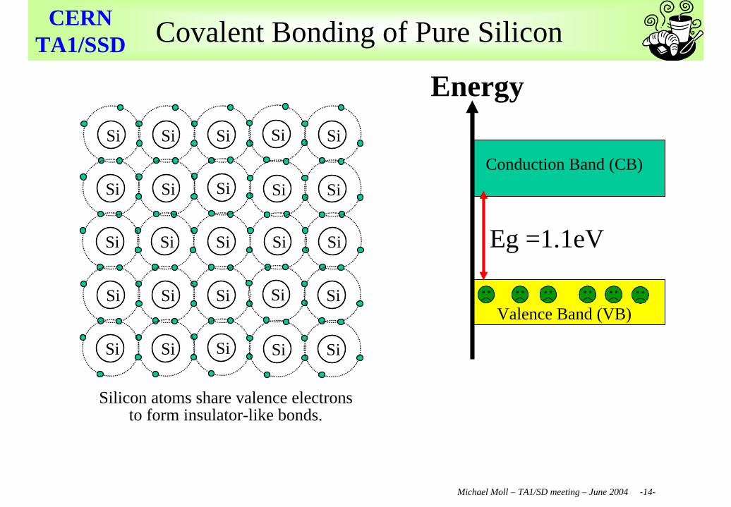
Silicon atoms share valence electrons to form insulator-like bonds.
Covalent Bonding of Pure Silicon
Eg =1.1eV
Conduction Band (CB)
Valence Band (VB)
Energy
Michael Moll – TA1/SD meeting – June 2004 -15-
CERNTA1/SSD
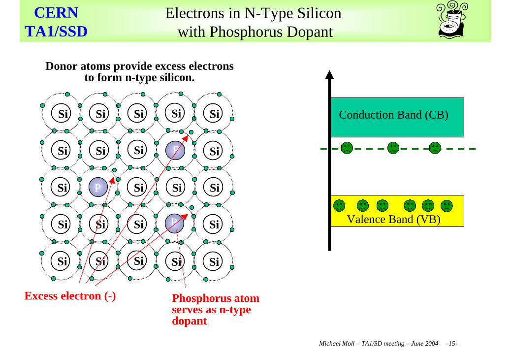
Donor atoms provide excess electrons to form n-type silicon.
Si
Si Si
Si
Si
Si
Si Si
Si
Si
Si
Si
Si
Si
Si
Si Si
Si
Si
Si
Si
Si
P
P
P
Electrons in N-Type Silicon with Phosphorus Dopant
Phosphorus atom serves as n-type dopant
Excess electron (-)
Conduction Band (CB)
Valence Band (VB)
Michael Moll – TA1/SD meeting – June 2004 -16-
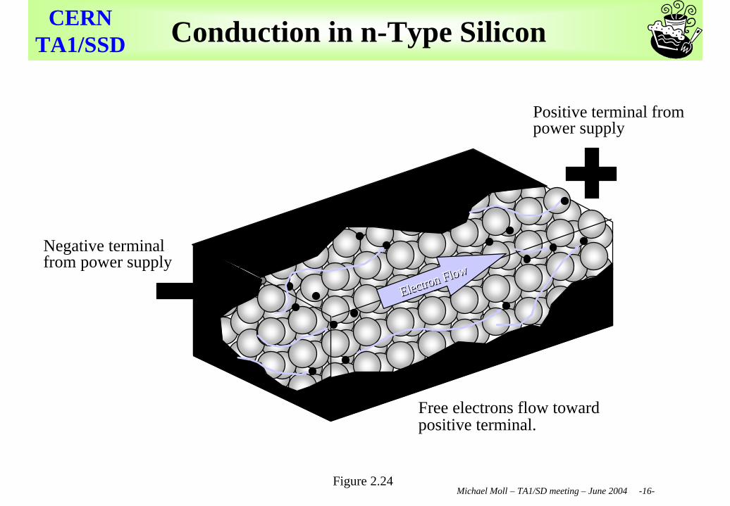
CERNTA1/SSD Conduction in n-Type Silicon
Free electrons flow toward positive terminal.
Positive terminal from power supply
Electron FlowElectron Flow
Negative terminal from power supply
Figure 2.24
Michael Moll – TA1/SD meeting – June 2004 -17-
CERNTA1/SSD
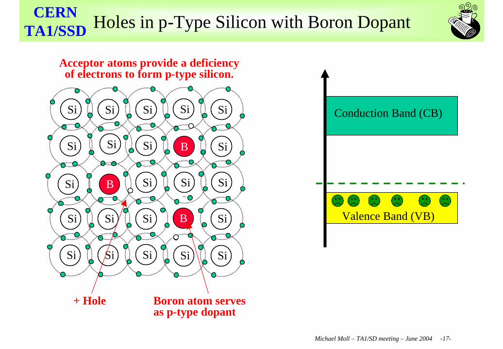
Acceptor atoms provide a deficiency of electrons to form p-type silicon.
+ Hole Boron atom serves as p-type dopant
Si
Si Si
Si
Si
Si
Si Si
Si
Si
Si
Si
Si
Si
Si Si
B Si
SiSi
Si
Si
Si
B
B
Holes in p-Type Silicon with Boron Dopant
Conduction Band (CB)
Valence Band (VB)
Michael Moll – TA1/SD meeting – June 2004 -18-
CERNTA1/SSD
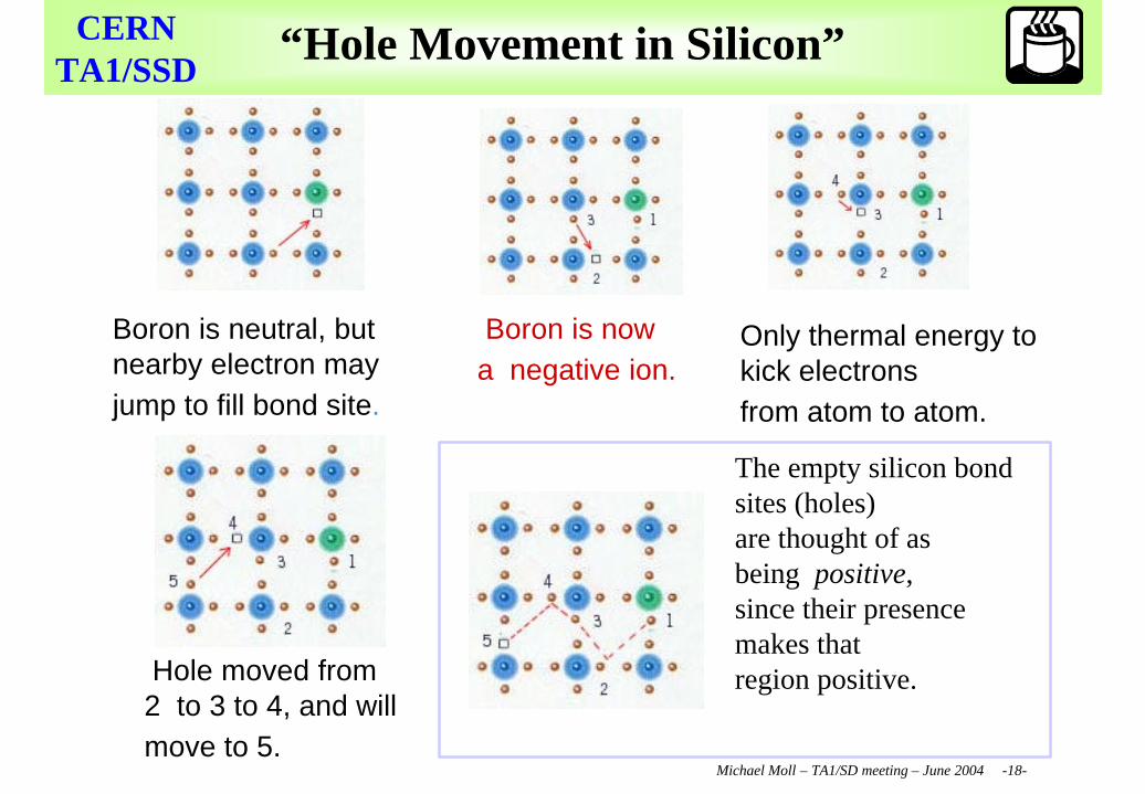
“Hole Movement in Silicon”
Boron is neutral, butnearby electron mayjump to fill bond site.
Boron is now a negative ion.
Only thermal energy to kick electronsfrom atom to atom.
Hole moved from 2 to 3 to 4, and will move to 5.
The empty silicon bond sites (holes) are thought of as being positive, since their presence makes that region positive.
Michael Moll – TA1/SD meeting – June 2004 -19-
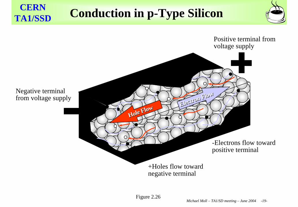
CERNTA1/SSD Conduction in p-Type Silicon
Electron Flow
Electron Flow
Hole FlowHole Flow
Positive terminal from voltage supply
Negative terminal from voltage supply
+Holes flow toward negative terminal
-Electrons flow toward positive terminal
Figure 2.26
Outline
CERN, TA1/SSD coffee meeting 11.6.2004
• Silicon and Silicon crystal structure
• Defect types in silicon crystals
• Silicon doping (Dopants = Defects)
• Radiation induced defects
•Point defects and clusters
•Particle dependence
•Defect kinetics
•Example of DLTS measurement
• What are defects doing to detectors?
• How to measure defects?
• Coffee
Michael Moll – TA1/SD meeting – June 2004 -21-
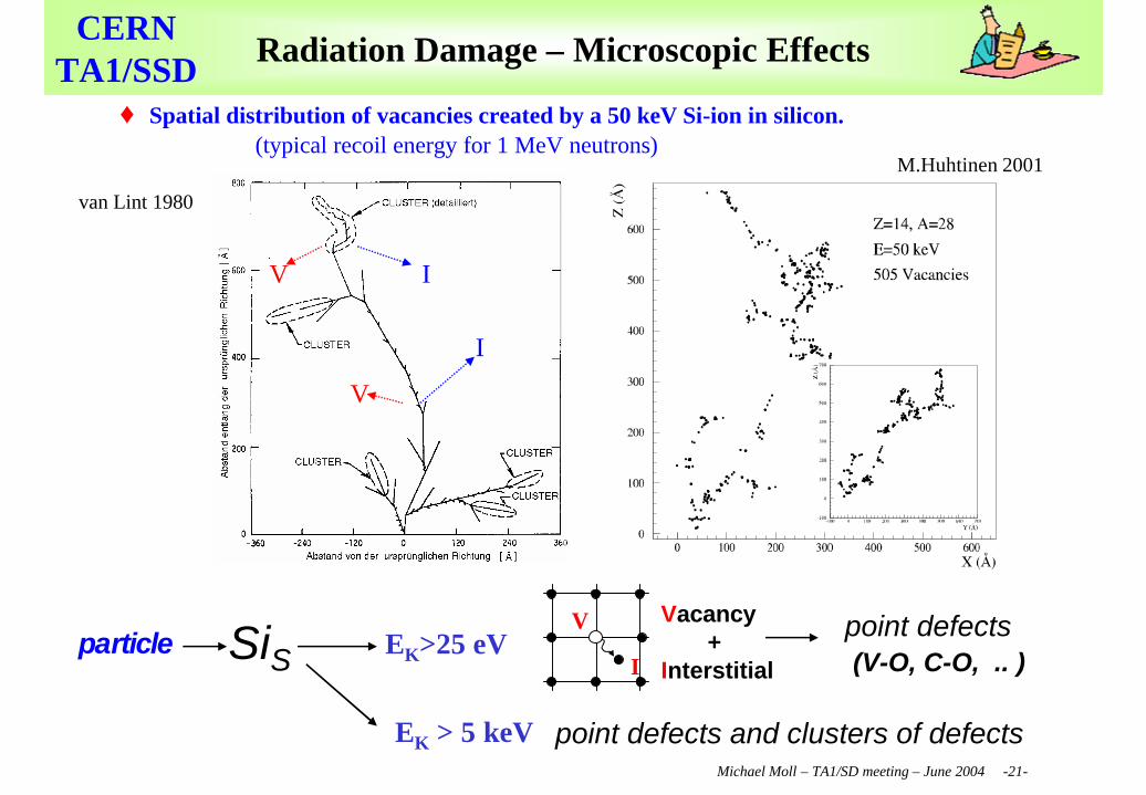
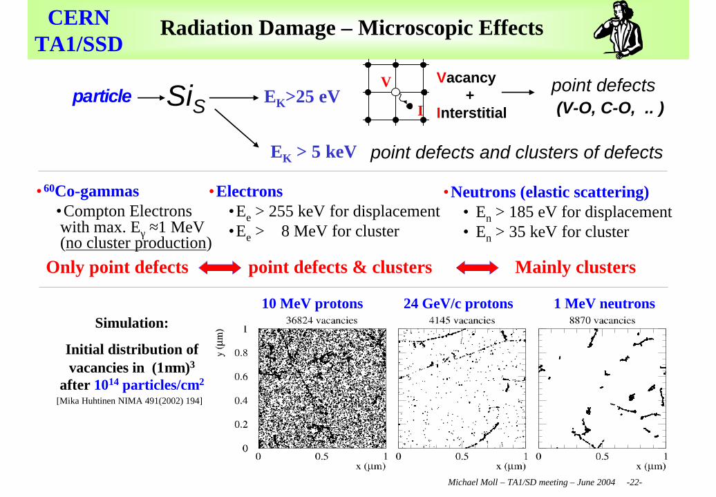
CERNTA1/SSD Radiation Damage – Microscopic Effects
particle SiSVacancy
+ Interstitial
point defects (V-O, C-O, .. )
point defects and clusters of defects
EK>25 eV
EK > 5 keV
V
I
I
I
V
V
♦ Spatial distribution of vacancies created by a 50 keV Si-ion in silicon.(typical recoil energy for 1 MeV neutrons)
van Lint 1980
M.Huhtinen 2001
Michael Moll – TA1/SD meeting – June 2004 -22-
CERNTA1/SSD
Radiation Damage – Microscopic Effects
particle SiSVacancy
+ Interstitial
point defects (V-O, C-O, .. )
point defects and clusters of defects
EK>25 eV
EK > 5 keV
V
I
•Neutrons (elastic scattering)• En > 185 eV for displacement• En > 35 keV for cluster
•60Co-gammas•Compton Electronswith max. Eγ ≈1 MeV(no cluster production)
•Electrons•Ee > 255 keV for displacement•Ee > 8 MeV for cluster
Only point defects point defects & clusters Mainly clusters
10 MeV protons 24 GeV/c protons 1 MeV neutronsSimulation:
Initial distribution of vacancies in (1µm)3
after 1014 particles/cm2
[Mika Huhtinen NIMA 491(2002) 194]
Michael Moll – TA1/SD meeting – June 2004 -23-
CERNTA1/SSD
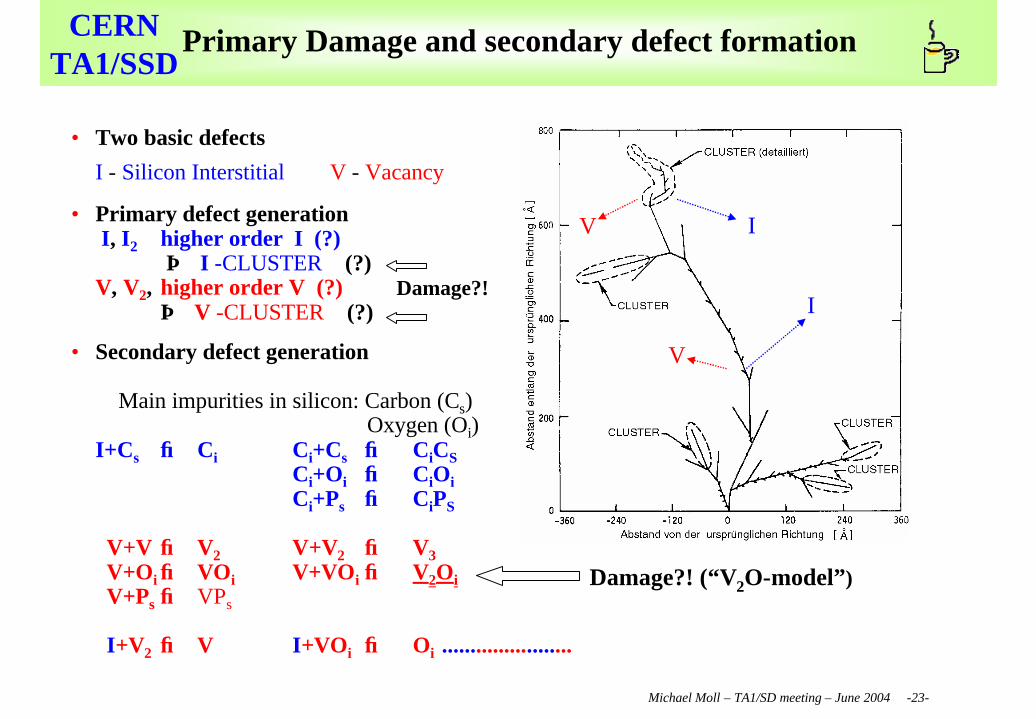
Primary Damage and secondary defect formation
• Two basic defects
I - Silicon Interstitial V - Vacancy
• Primary defect generationI, I2 higher order I (?)
⇒ I -CLUSTER (?)V, V2, higher order V (?)
⇒ V -CLUSTER (?)
• Secondary defect generation
Main impurities in silicon: Carbon (Cs)Oxygen (Oi)
I+Cs → Ci ⇒ Ci+Cs → CiCSCi+Oi → CiOiCi+Ps → CiPS
V+V → V2 V+V2 → V3 V+Oi → VOi ⇒ V+VOi → V2OiV+Ps → VPs
I+V2 → V I+VOi → Oi .......................
I
I
V
V
Damage?! (“V2O-model”)
Damage?!
Michael Moll – TA1/SD meeting – June 2004 -24-
CERNTA1/SSD
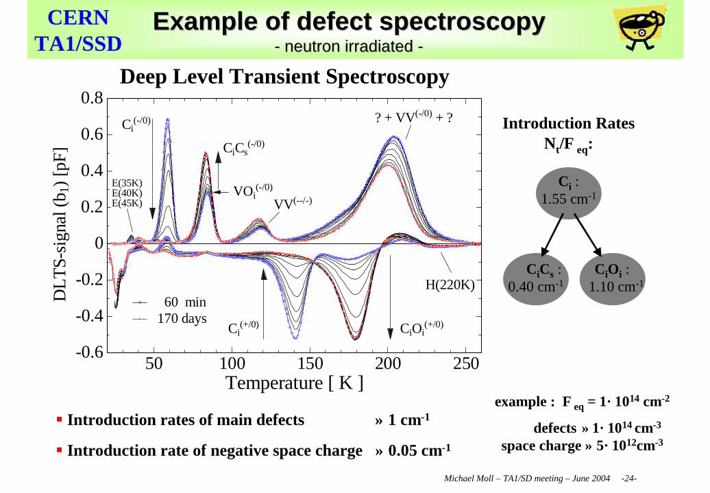
Example of defect spectroscopyExample of defect spectroscopy-- neutron irradiated neutron irradiated --
50 100 150 200 250Temperature [ K ]
-0.6
-0.4
-0.2
0
0.2
0.4
0.6
0.8
DLT
S-si
gnal
(b1)
[pF]
60 min 60 min170 days170 days
CiCs(-/0)CiCs(-/0)
VOi(-/0)VOi(-/0)
VV(--/-)VV(--/-)
Ci(-/0)Ci(-/0)
CiOi(+/0)CiOi(+/0)
H(220K)H(220K)
Ci(+/0)Ci(+/0)
E(40K)E(40K)E(45K)E(45K)
E(35K)E(35K)
? + VV(-/0) + ?? + VV(-/0) + ? Introduction RatesNt/Φeq:
Ci :1.55 cm-1
CiCs : CiOi :0.40 cm-1 1.10 cm-1
§ Introduction rates of main defects ≈ 1 cm-1
§ Introduction rate of negative space charge ≈ 0.05 cm-1
example : Φeq = 1×1014 cm-2
defects ≈ 1×1014 cm-3
space charge ≈ 5×1012cm-3
Deep Level Transient Spectroscopy
Outline
CERN, TA1/SSD coffee meeting 11.6.2004
• Silicon and Silicon crystal structure
• Defect types in silicon crystals
• Silicon doping (Dopants = Defects)
• Radiation induced defects
• What are defects doing to detectors?
• How to measure defects?
• Coffee
Michael Moll – TA1/SD meeting – June 2004 -26-
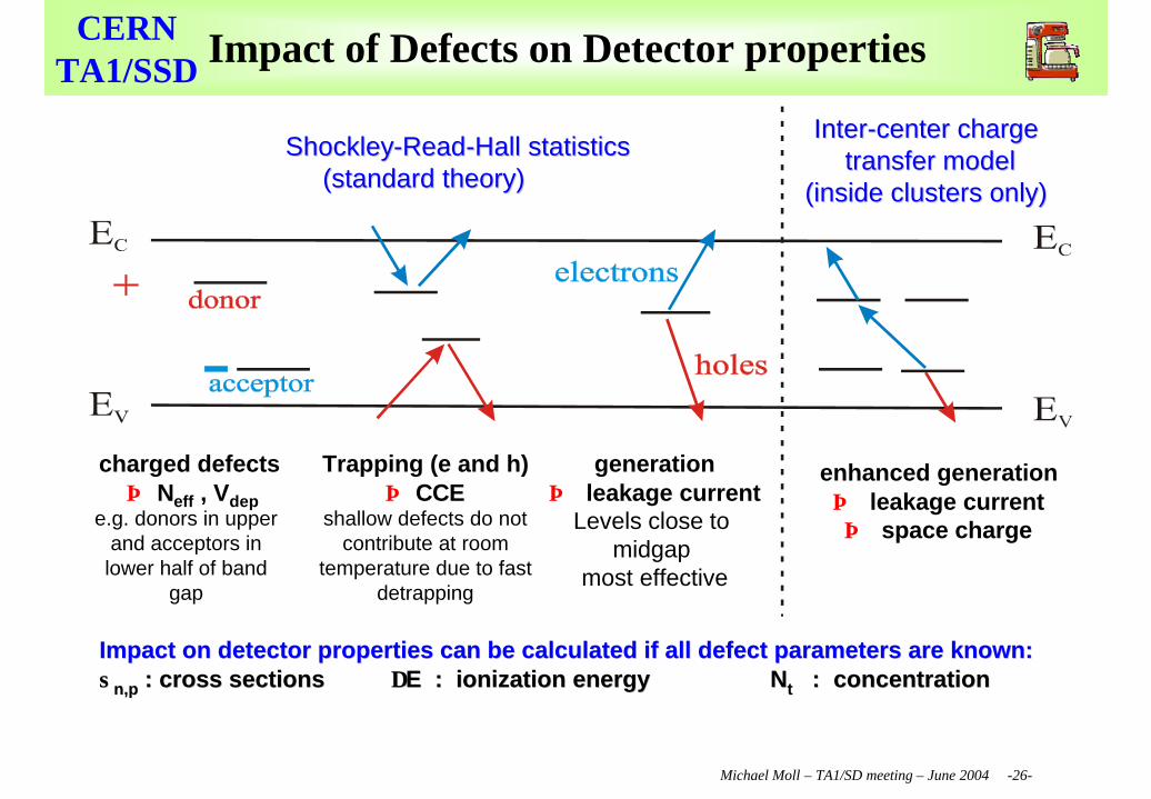
CERNTA1/SSD Impact of Defects on Detector properties
ShockleyShockley--ReadRead--Hall statistics Hall statistics (standard theory)(standard theory)
Impact on detector properties can be calculated if all defect paImpact on detector properties can be calculated if all defect parameters are known:rameters are known:σσn,pn,p : cross sections : cross sections ∆∆E : ionization energy E : ionization energy NNtt : concentration: concentration
Trapping (e and h)⇒ CCE
shallow defects do not contribute at room
temperature due to fast detrapping
charged defects ⇒ Neff , Vdep
e.g. donors in upper and acceptors in lower half of band
gap
generation⇒ leakage current
Levels close to midgap
most effective
enhanced generation⇒ leakage current⇒ space charge
InterInter--center chargecenter chargetransfer model transfer model
(inside clusters only)(inside clusters only)
Outline
CERN, TA1/SSD coffee meeting 11.6.2004
• Silicon and Silicon crystal structure
• Defect types in silicon crystals
• Silicon doping (Dopants = Defects)
• Radiation induced defects
• What are defects doing to detectors?
• How to measure defects?
• Some measurement techniques …
• Deep Level Transient Spectroscopy
• Coffee
Michael Moll – TA1/SD meeting – June 2004 -28-
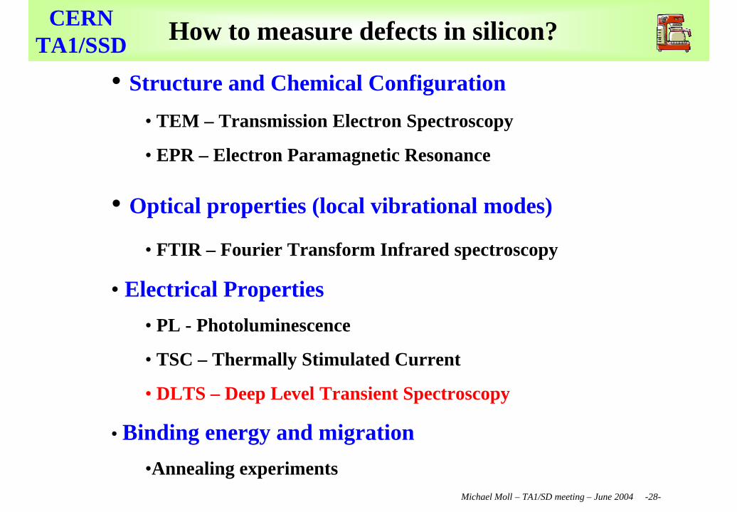
CERNTA1/SSD How to measure defects in silicon?
• Structure and Chemical Configuration
• TEM – Transmission Electron Spectroscopy
• EPR – Electron Paramagnetic Resonance
• Optical properties (local vibrational modes)
• FTIR – Fourier Transform Infrared spectroscopy
• Electrical Properties
• PL - Photoluminescence
• TSC – Thermally Stimulated Current
• DLTS – Deep Level Transient Spectroscopy
• Binding energy and migration
•Annealing experiments
Michael Moll – TA1/SD meeting – June 2004 -29-
CERNTA1/SSD
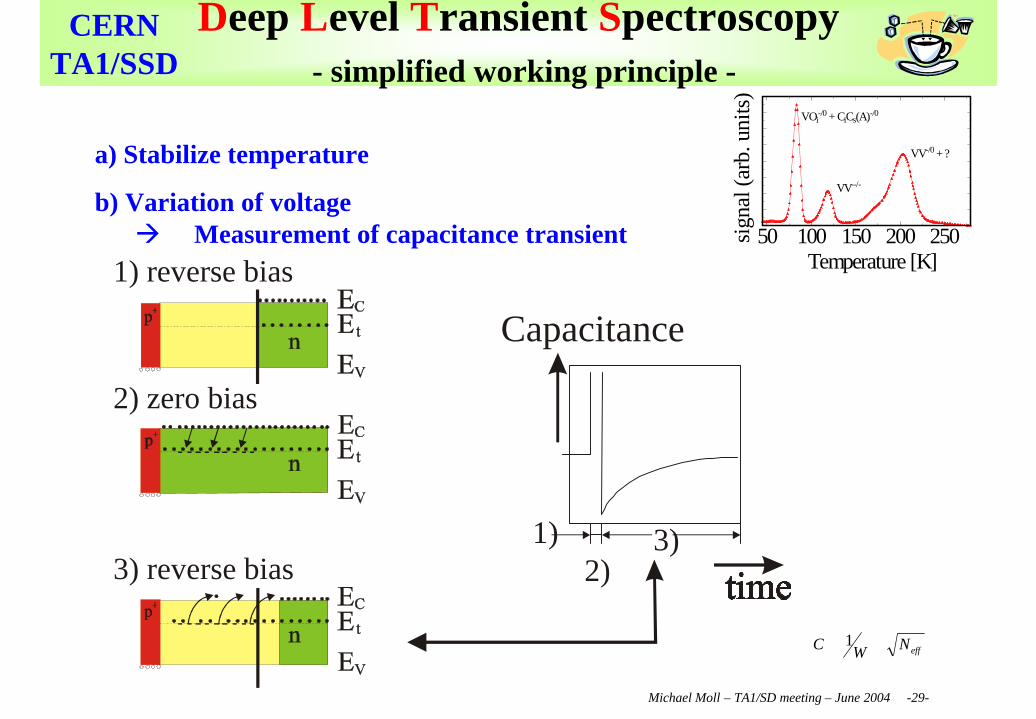
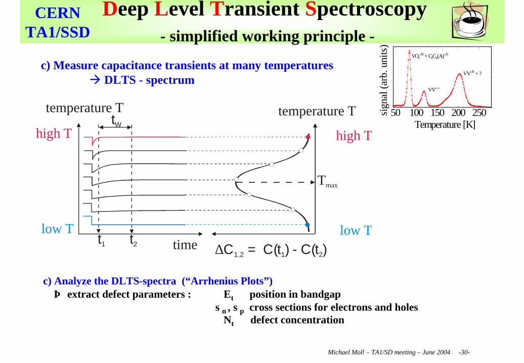
Deep Level Transient Spectroscopy- simplified working principle -
effNWC ∝∝ 1
a) Stabilize temperature
b) Variation of voltage à Measurement of capacitance transient 50 100 150 200 250
Temperature [K]
sign
al (a
rb. u
nits
)
VOi-/0 + CiCs(A)-/0 VOi-/0 + CiCs(A)-/0
VV--/- VV--/-
VV-/0 + ? VV-/0 + ?
Capacitance
1) 3)2)
1) reverse bias
3) reverse bias
2) zero bias
Michael Moll – TA1/SD meeting – June 2004 -30-
CERNTA1/SSD
c) Measure capacitance transients at many temperatures à DLTS - spectrum
c) Analyze the DLTS-spectra (“Arrhenius Plots”)⇒ extract defect parameters : Et position in bandgap
σn , σp cross sections for electrons and holesNt defect concentration
time
tW
temperature T
high T
low T∆C = C(t ) - C(t )1,2 1 2
t1 t2
Tmax
temperature T
high T
low T
Deep Level Transient Spectroscopy- simplified working principle -
50 100 150 200 250Temperature [K]
sign
al (a
rb. u
nits
)
VOi-/0 + CiCs(A)-/0 VOi-/0 + CiCs(A)-/0
VV--/- VV--/-
VV-/0 + ? VV-/0 + ?
Michael Moll – TA1/SD meeting – June 2004 -31-
CERNTA1/SSD Coffee !!!!!
Coffee !!!!!