Embed Size (px)
Citation preview

CFA vs. VFA: a short primer for the uninitiated
A concise introduction to
VFA and CFA audio power
amplifiers, in which the two
topologies are compared
and their strengths and
weaknesses evaluated.
Andrew C Russell
Updated January 2014
V2.00

CFA vs. VFA: a short primer for the uninitiated
Page 1 www.hifisonix.com
CFA vs. classic Lin VFA topology:
A short primer for the uninitiated
Introduction. CFA topology amplifiers have been around in the IC industry for 30 years. Following a
patent claim by David Nelson, the earliest commercial offering was a module from Comlinear in 1982
and a few years later, IC’s from both Comlinear and Elantec. Prior to this, they were also described and
analyzed in a number of papers. With regard to discrete based audio amplifiers, the topology has been
used by a few esoteric brands in audio, with Accuphase, a Japanese company based in Yokohama, being
a notable exponent. Cyrus, a small UK company, has also marketed CFA based power amplifiers. There
are examples of Pioneer amplifiers from the early 1970’s that used CFA, which apparently even pre-date
the IC offerings and Mark Alexander published a design as an ADI application note in the 1980’s, while
Marantz have also marketed CFA power amplifiers. CFA topology audio amplifiers continue to be
somewhat upstaged by their more widely understood and deployed VFA counterparts – a situation not
helped by the fact that neither Cordell nor Self touched the subject in their otherwise wide ranging
audio design books. A CFA’s operation is not as intuitive as a VFA and there are some subtleties in regard
to whether a transimpedance (TIS) or transadmitance (TAS) second stage is used and certainly the
guidelines used by power amplifier designers to set the ULGF on VFA’s do not apply to CFA’s. The upshot
of these and other factors meant designers preferred to go with something that is generally more widely
documented and traditional – i.e. VFA. There is a lot of misinformation out in the audio industry and DIY
community about CFA’s, with some notable commentators dismissing them altogether, which is a pity
since they do bring very specific properties to the table that are of benefit in audio power amplifiers.
There are many explanations about IC CFA topologies like this or this. Some plunge into math, loop gain
equations and so forth, leaving the reader none the wiser, while this one (equations 1~4 and associated
gain plots) from Hans Palouda is altogether easier to understand, as is ADI’s here. For VFA’s, Bruno
Putzeys’ explanation is by far the most succinct, even though the main thrust of his article is to dispel
some enduring myths about negative feedback. Which brings me to the reason for this short document:
‘CFA vs. classic VFA1 – a short primer for the uninitiated’ in which I will try to explain the differences
between the two topologies, dispel the myths and hopefully encourage more audio power amplifier
designers to experiment with this technique.
So, how do you tell if an amplifier is VFA or CFA?
1 I have deliberately used the term ‘classic VFA’ to mean MC or dominant pole compensated VFA which will be used a vehicle to explain the
fundamental differences between the two topologies. There are alternative VFA compensation schemes that allow the it=CV SR limit in MC to
be broken so that similar SR performance is attainable by VFAs, while TPC allows the loop gain BW to be widened to that of CFA’s as well. You
can read about some of these techniques in Bob Cordell’s book ‘Designing Audio Power Amplifiers’ Chapter 4.
Rf
Rg

CFA vs. VFA: a short primer for the uninitiated
Page 2 www.hifisonix.com
Test/Pointer VFA CFA Test 1 Peak input current to TIS = LTP tail current Peak input current to TIS/TAS =
Vopeak/Rfeedback
Test 2 Closed loop -3 dB bandwidth constrained by constant gain bandwidth product
Closed loop -3 dB bandwidth independent of closed loop gain* (See footnote 2 below)
Pointer 1 Both + and – inputs are high impedance nodes
+input is high impedance, -input is low impedance
Pointer 2 Two gain stages (LTP+TIS) = higher OLG One gain stage – 2nd
stage TIS/TAS = lower OLG
Table 1 – How to identify CFA from VFA – two tests and two pointers method
The two tests and two pointers method will allow you in most cases to accurately identify
whether an amplifier circuit is CFA or not. Other than the mathematical derivations of the loop
gains (see references) which are very different, the defining behavioral characteristic of classic
CFA amplifiers are their gain-bandwidth product independence2 and the fact that peak TIS input
current (a key factor in SR performance) is not limited by the an input stage tail current, as is
the case in a VFA. The detailed descriptions of the tests and pointers will be evident in the
discussion of the two topologies that follow in this document. What is important here is that
the above approach covers most variants of the two topologies – so single ended types,
balanced, unbalanced circuits, JFET or bipolar inputs. If a circuit behaves like a CFA (or a VFA)
then the assumption here is that it is a CFA (or VFA as the case may be). The pointers act as
secondary guides, if identification is still difficult – in most cases however, tests 1 and 2 are
sufficient to accurately categorize an amplifier topology.
Some amplifier designs are more difficult to identify – for example VFA’s using folded cascode
techniques are single gain stage VFA’s; similarly, there are CFA’s with two gain stages, and Jean
Hiraga’s famous 20W class A design from the early 1980’s had an output stage with gain – so it
was a two gain stages CFA . However, in both of these cases, they would pass Test 1 and Test 2
correctly for their specific topologies, allowing accurate identification. There are exceptions to
the rule. H bridge input amplifiers appear topologically similar to a classic CFA with the
inverting feedback network input buffered by a second diamond stage, mirroring the non-
inverting input diamond buffer. A resistor connected between the summing junction of the
two buffers sets the front end stage gm, allowing very wide bandwidths and high slew rates.
The H bridge input stage would test out using the postulates in Table 1 as a CFA – the peak TIS
current is set by the buffer coupling resistor, and it is not constant gain bandwidth limited like a
VFA – a fact I easily confirmed in simulation. However, the IC industry classifies it as a VFA and
so we will leave it at that – in certain cases the debate as to whether an amplifier circuit is VFA
or CFA will remain a contentious one.
2 Note this applies at low gains and at reduced PM’s – the so called ‘gain range sweet spot’ often referred to in IC CFA application notes which is up to about 25 dB. At higher gains and or loop PM’s, CFA’s tend to degenerate into constant gain bandwidth behavior, albeit at higher closed loop bandwidths than VFA’s. We will return to discuss these points later in the document.
CFA vs. VFA: a short primer for the uninitiated
Page 3 www.hifisonix.com
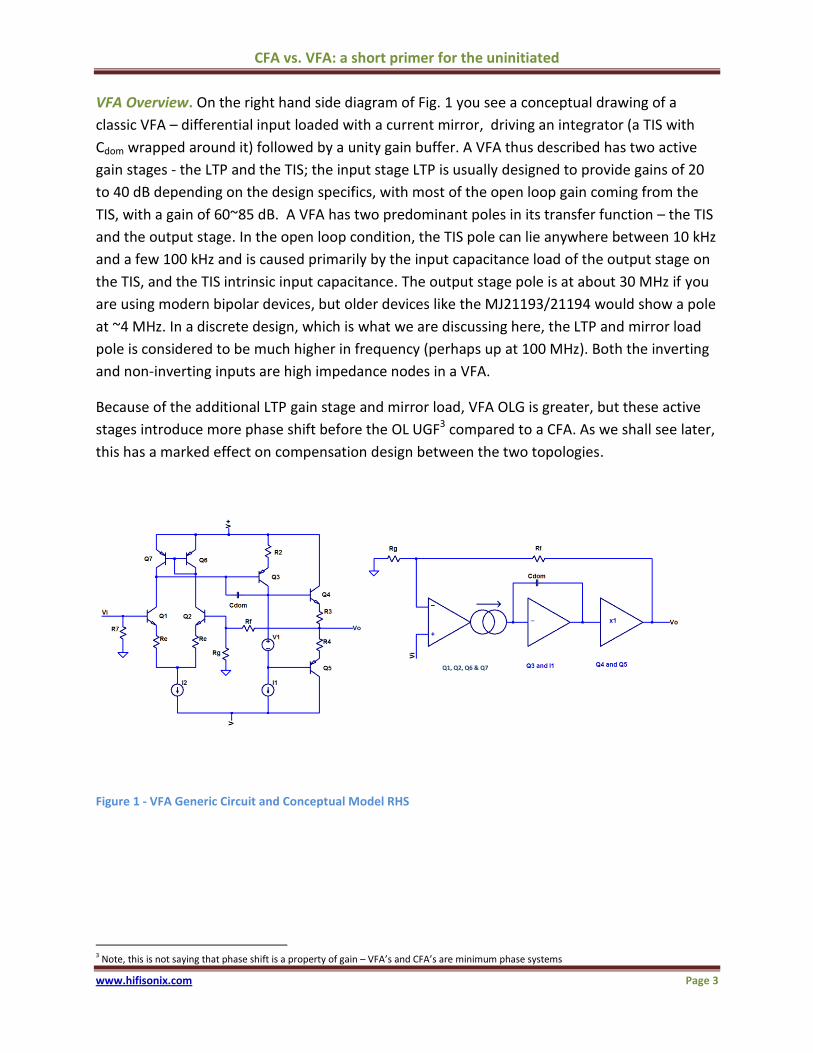
VFA Overview. On the right hand side diagram of Fig. 1 you see a conceptual drawing of a
classic VFA – differential input loaded with a current mirror, driving an integrator (a TIS with
Cdom wrapped around it) followed by a unity gain buffer. A VFA thus described has two active
gain stages - the LTP and the TIS; the input stage LTP is usually designed to provide gains of 20
to 40 dB depending on the design specifics, with most of the open loop gain coming from the
TIS, with a gain of 60~85 dB. A VFA has two predominant poles in its transfer function – the TIS
and the output stage. In the open loop condition, the TIS pole can lie anywhere between 10 kHz
and a few 100 kHz and is caused primarily by the input capacitance load of the output stage on
the TIS, and the TIS intrinsic input capacitance. The output stage pole is at about 30 MHz if you
are using modern bipolar devices, but older devices like the MJ21193/21194 would show a pole
at ~4 MHz. In a discrete design, which is what we are discussing here, the LTP and mirror load
pole is considered to be much higher in frequency (perhaps up at 100 MHz). Both the inverting
and non-inverting inputs are high impedance nodes in a VFA.
Because of the additional LTP gain stage and mirror load, VFA OLG is greater, but these active
stages introduce more phase shift before the OL UGF3 compared to a CFA. As we shall see later,
this has a marked effect on compensation design between the two topologies.
Figure 1 - VFA Generic Circuit and Conceptual Model RHS
3 Note, this is not saying that phase shift is a property of gain – VFA’s and CFA’s are minimum phase systems
Q1, Q2, Q6 & Q7

CFA vs. VFA: a short primer for the uninitiated
Page 4 www.hifisonix.com
Hifisonix amplifiers from front to rear: 100 W class AB CFA nx-Amplifier, 15 W CFA Class A sx-
Amplifier; Rear LHS 280 W class AB VFA Ovation 250 and rear RHS the 180 W class AB VFA e-Amp

CFA vs. VFA: a short primer for the uninitiated
Page 5 www.hifisonix.com
In a Lin VFA topology, the input pair tail current is fixed by a current source I1 with the signals
on the LTP input essentially steering a portion of this fixed current into or away from the TIS
input node at the base of Q3 - hence the current source output depiction in the conceptual VFA
in Fig. 1. The maximum output current of the diff amp stage available to drive the TIS (Q3
loaded by I1 in the circuit on the left in Fig. 1) and any compensation networks (MC, TPC, TMC,
shunt, etc. but in this classic Lin VFA example, Cdom)4 is equal to this tail current I1, assuming
the LTP is loaded with a mirror. If it’s resistively loaded it’s lower and in a correctly balanced
LTP about half the tail current.
CFA Overview. In a CFA (Fig. 2) , the input devices are arranged in a diamond buffer
configuration (Q1~Q4) with unity gain – the non-inverting input is a high impedance node, and
the buffer output is connected to a low impedance inverting input node at the junction of Rg
and Rf. Note that the front end buffer transistors (Q1 and Q2) are not inside the global
feedback loop, as in the case of the VFA. The output current of the diamond stage appears at
the collectors of the level shifters Q3 and Q4 and is not limited by a current source as is the
case in a VFA, but instead set by the output voltage level and the value of the feedback resistor
+ Ro. Ro is usually small - in IC’s a fraction of an Ω, but in practical power amplifiers in order to
stabilize the DC operating point, usually up to 10’s of Ω’s.
Figure 2 - CFA Generic Circuit and Conceptual Model on RHS
In IC opamps, a current mirror (TAS) is almost always used to convert the front end diamond
buffer output current to a voltage that is then buffered by the output stage. This has the
advantage, in general, of providing high gains from Imirror x Rad, and isolating the front end stage
4 MC = Miller compensation; TPC = Two Pole compensation; TMC = Transitional Miller Compensation; OIC = Output Inclusive Compensation
Note: In this model, the circuit on LHS shows
TIS 2nd stage, while the conceptual model on
the RHS shows a mirror (TAS) 2nd stage. This
does not alter the basic description of CFA
operation in this document. The TIS 2nd stage
was selected in the sim models to allow
easier comparison between CFA and VFA
topologies following on from the Fig 1 VFA
discussion.

CFA vs. VFA: a short primer for the uninitiated
Page 6 www.hifisonix.com
from the output stage much more so than a TIS. Further, since the intrinsic mirror bandwidth is
very wide compared to a typical TIS configuration – MHz in the case of an IC opamp because
there is little or no Miller effect – the stage pole is therefore also high. In the small signal
regime of an IC opamp, this works well because the output load is a few mA and well defined
with minimal load reflection back into the 2nd stage. However, the situation in an audio power
amplifier is very different: the output stage input impedance varies significantly over the
voltage swing and the output load impedance (most often reactive with big swings in load
impedance) is reflected back onto its input to a much greater degree, thus, the load on the
output of the TAS mirror is highly non-linear and the overall impact in terms of distortion
reduction and bandwidth is less than one would expect. Therefore, in current feedback discrete
power amplifiers, a conventional TIS makes much more sense, and as a result, instead of the
uncompensated 2nd stage pole lying in the 100’s of kHz as in the case of a TAS mirror, it
typically lies in the 10’s of kHz range – i.e. about an order of magnitude lower. Unlike VFA’s,
the phase shift accumulation in a CFA proceeds more slowly due to fewer active gain stages,
affording greater PM and GM at HF.
TIS vs TAS. It is interesting here to contrast the behavior of an MC VFA, where the TIS output
impedance (and stage gain) actually decreases with frequency due to the increasing local
feedback provided by the reduction in Cdom Xc - thus the OPS is driven from a low source
impedance at HF, mitigating somewhat the issues alluded to earlier. In a TAS CFA, you ideally
want the mirror output to be flat in order to preserve bandwidth – difficult in practice on a
power amplifier unless you are prepared to carry the burden of extra circuit complexity – and
then you are still left with the output stage phase shift to deal with (see later). One solution to
this problem is to configure the main gain stage in a CFA as a TIS, but to preserve the SR
performance, apply Alexander compensation5 where the local feedback loop is taken from the
TIS output back to the inverting input – somewhat analogous to MIC in a VFA.
Setting Closed Loop Gain Magnitude. For both the VFA and CFA, the non-inverting closed loop
gain is defined as Avcl = 1+(Rf/Rg), and for inverting simply as Rf/Rg, where Rf is the resistor
connected between the output and the inverting input, and Rg is the resistor between the
inverting input and ground as shown in Figs. 1 and 2. Although the closed loop gain for both
configurations is expressed the same way, the underlying derivations (see Hans Palouda’s
article for example) are not the same, and this explains the differences in the loop gain
behavior.
5 See the appendix of the application note for the full derivation of this compensation technique

CFA vs. VFA: a short primer for the uninitiated
Page 7 www.hifisonix.com
Loop Gain and Compensation Compared. As we have seen, VFA’s (see figures 7 & 8) have higher
open loop gains, and hence loop gains at LF because of the additional gain provided by the LTP
stage, but phase shift accumulation also proceeds more rapidly as a result. To deal with this and
ensure closed loop stability, dominant pole compensation (MC) is employed. In MC, the ULGF
intercept is located by design (see the formula below) somewhere between 1 MHz and 3 MHz
where there is adequate PM (60 degrees or more in a practical power amplifier) with an assumed
slope of 20 dB/decade which then intercepts the loop LF gain at a frequency from a few hundred Hz
down to a few 10s of Hz – the exact figure dependent upon the LF OLG. ‘Dominant’ pole
compensation pushes the first open loop pole down in frequency, and the second open loop pole
up beyond the ULGF resulting in so called ’pole splitting’ - which you can see demonstrated
graphically in curves 3 and 4 in Fig. 3 on the next page. The PM at HF is also thus improved and in
the ideal case is 90 degrees at the ULGF. The result is a constant gain bandwidth product closed
loop response which is a feature of dominant pole compensated amplifiers such that if we fix the
ULGF and the required closed loop gain, the value of Cdom in Fig. 1 (assuming 20 dB/decade roll off)
( ) 6
Where fulgf = the unity loop gain frequency (ULGF)
Acl = is the closed loop gain magnitude below the -3db roll off point – i.e. low frequency gain
Rdegen is the LTP emitter degeneration resistor - in Fig. 1 these are not shown as Re
re’ is the internal emitter resistance of the LTP transistors from [0.026/(2*LTP tail current)]
You can see the constant gain bandwidth term above from fulgf x Acl.
For Alexander compensated CFA’s, assuming a 20 dB/decade response roll off, Ccomp in Fig 2 can be
estimated from
( ( )
Note from this formula, there is no gain term Acl as in the VFA example. Shunt compensation from
the TIS output to ground can also be used but the same ULGF in a CFA requires about five times the
Ccomp value compared to using Alexander compensation which also preserves the high slew rate
performance of this topology. Some practitioners consider this type of compensation very sub-
optimal. In my designs, I prefer to use Alexander compensation.
ULGF Intercepts in CFA and VFA compared. In CFA amplifiers, the fewer active gain stages and
lower open loop and loop gain, mean that phase accumulation is less than in VFA’s: the designer
therefore does not have to employ dominant pole compensation to push the HF pole further below
the unity gain frequency intercept to improve the PM for stability, instead trading the greater gain
and PMs for wider loop gains.
6 This formula is referenced in many texts e.g. D. self, R. Cordell, M. Leach etc.

CFA vs. VFA: a short primer for the uninitiated
Page 8 www.hifisonix.com
Figure 3 - VFA Pole Splitting
In Fig. 3 you can see the action of pole splitting in a VFA by comparing LG response curves 3 & 4 – the dominant pole at ~8 kHz is pushed down to ~200 Hz, while the HF pole at ~500 kHz is pushed up to ~2 MHz. The ULGF in this example is 1 MHz. Pole splitting reduces the effect of HF phase shift, ensuring stability.
The closed loop response (curves 5 and 6) show little deviation from each other until ~200 KHz, after which the uncompensated CL response diverges, peaking at 40dB at 5 MHz with rapid phase change. The Compensated LG roles off at 20 dB/decade with a CL UG frequency of about 15 MHz.
Note, if a CFA uses MC, the pole splitting behavior also results – so it’s not unique to VFA’s, but
simply a property of dominant pole compensation.
It should be noted at this point that audio power amplifier applications are quite unique in that
they demand PM’s of at least 60 degrees in order to cater for a wide range of reactive loads.
Therefore, no matter what compensation technique is deployed (MIC, TPC, OIC etc), the ULGF
PM should always be in the region of 60 degrees or more to ensure the design is capable of
dealing with real world loads. I usually incorporate an output coupling inductor of between
0.6uH and 1uH in my designs which is extremely effective in isolating the amplifier output from
capacitive loads, ensuring stability.
2- Uncompensated
OLG
1- Compensated OLG
3. Uncompensated
LG
5&6 - Closed loop
gain compensated
and uncompensated
4- Compensated LG

CFA vs. VFA: a short primer for the uninitiated
Page 9 www.hifisonix.com
The gain ‘sweet spot’
sometimes mentioned
in IC applications
notes refers to the
gain bandwidth
independence noted
in CFA’s. It’s called a
sweet spot because
this characteristic only
holds for loop PM’s in
the 30-50 degree
range and low CLG’s.
Once the application requires high PM’s – like the 60-90 degrees required for in an audio power
amplifier - this characteristic is less evident as the loop compensation has to be conservative - see
Fig. 4. In the IC application realm, it is for reasons of maximizing bandwidth that CFA’s are generally
compensated for much lower gain and phase margins thus preserving bandwidth – typical
applications being video amplifiers and high speed data converters where the focus in terms of
compensation design is on overshoot and settling performance, rather than PM.
In Fig.5 you see this
characteristic
demonstrated where
the PM on the CFA
model has been
deliberately set to 32
degrees. Here the gain
bandwidth
independence is
clearly visible at gains
of up to about 28 dB,
thereafter the
bandwidth is linked to
the gain.
On designs where the CLG is low but ULGF PM still rather high, the gain bandwidth independence is
also better maintained, and you can see an example of this in a practical low CLG amplifier, the sx-
Amp, on page 8 of that write-up. Lets be clear here: 30 degree PM’s in practical audio power
amplifiers will lead to problems – at least 60 degrees is required, with many designers targeting
even higher figures in the 80~90 degree region.
Figure 4 - VFA vs CFA closed loop Responses
The models in Appendix 2 were stepped from ~15 dB
to 34 dB, yielding the responses depicted here. Both
amplifiers compensated for the same PM at their
ULGF which is 85 degrees
Green is CFA, Magenta is VFA
Figure 5 - CFA comp'd for ~30 degree PM showing gain bandwidth independence
The CFA model in Appendix 2 – Ccomp set to 25pF
establishing a ULGF of 5.3 MHz and a PM of 32
degrees. The VFA remains unchanged
Green is CFA, Magenta is VFA

CFA vs. VFA: a short primer for the uninitiated
Page 10 www.hifisonix.com
In low PM and or low gain CFA systems, CLG can be varied over a wide range, provided Rf is
kept constant to minimize any disturbance of the compensation, and Rg varied instead with
reduced or little impact on the -3 dB bandwidth of the amplifier as shown in Fig. 4. In general,
for low closed loop gain designs (typical in audio), the CFA is notable for its wide loop
bandwidths – often > 10 kHz, and in the sx-Amp for example, it’s ~60 kHz (see Fig. 13 red trace
in the sx-Amplifier write up). Some designers claim that setting the loop gain -3 dB point above
the audio bandwidth reduces Phase Intermodulation Distortion (PIMD), but this has been
contested – see R. Cordell’s TIM I and TIM II for example.
The conventional way to compensate an IC CFA is to adjust the value of Rf to achieve the
optimum gain and PMs, usually by observing the overshoot and settling time to a fast rise/fall
time square wave input stimulus. Part of the reason for this approach, rather than using some
type of external compensation capacitor or network, and especially so in very high performance
IC CFA’s, is to avoid parasitic capacitance or inductance creeping into the TAS/TIS node which is
what would happen if a compensation connection were brought out to one of the IC pins –
remember, we are talking about devices with gain bandwidth products in the GHz region. In
practical power amplifiers, capacitive shunt compensation from the TIS output to ground is
often employed, although there are more advanced techniques like Alexander compensation as
used in the sx-Amplifier. CFA amplifiers - and especially discrete power amplifiers - almost
always exhibit gain peaking when the closed loop response is plotted, and this is linked of
course to the output stage pole7. The cure is to bandwidth limit the input signal with a simple
RC filter – you can see how I did this in the sx-Amplifier design (see Fig 14 in that document).
It’s also important to note that you can apply dominant pole MC to CFA’s as well – but to do so
one ends up with an amplifier in which the response morphs into that of a classic MC pole
splitting VFA, but with lower HF gain. For this reason, and SR performance, MC on a CFA is not
recommended.
Slew Rate (SR). The other major difference between the two topologies is the slew rate (SR),
set in a VFA by the compensation capacitor value and the LTP tail current from SR= i/c. As
already pointed out, in a CFA the peak current available to the input of the TIS is set by the
maximum output voltage and the value of the feedback resistor (assuming Ro is very low in
value compared to Rg). In a correctly compensated CFA using TAS for the 2nd stage, this can be
a factor of 10 higher than a classic VFA, and explains the big differences in SR between the two
topologies, with 200 V/us the norm in a CFA audio power amplifier.
7 Unlike discrete power amplifiers, the output stage device Ft’s in IC devices are very high and peaking in IC’s (CFA and VFA) is therefore more generally associated with stray capacitance from the –input to ground, and/or stray capacitance across Rf. Layout is critical to minimize these effects and to preserve the bandwidth performance – follow data sheet recommendations carefully to avoid these problems.
CFA vs. VFA: a short primer for the uninitiated
Page 11 www.hifisonix.com
Output Stage Pole Impact on Loop Gain Bandwidth in Discrete Power Amplifiers. Importantly, in
both topologies, the output stage phase shift ultimately limits the amount of feedback and the loop
bandwidth of the amplifier. In a bipolar VFA, one usually sets the ULGF based on the output stage
response; a good rule of thumb is to set it at between 5-10% of the Ft of the output devices up to a
maximum of 3 MHz depending on the type of output stage8 – EF2 or EF3. For example, If you use a
MJL1302/3281 bipolar output stage with Ft’s of 30 MHz, set the ULGF for an EF3 at 1~1.5 MHz,
while for an EF2, you can go to 3 MHz. Mosfet output devices have Ft’s at about 300 MHz, but in
practice you cannot set the amplifier ULGF at 30 MHz because of circuit parasitics (layout
inductances and capacitances) and the high input capacitance of these devices9. In this case, one
would set the ULGF at 3 MHz, which is a practical upper limit for VFA audio power amplifiers. As
already touched upon earlier in this document, there is greater gain and PM at HF in CFA’s, and the
loop can be closed at higher frequencies. Whereas in VFA’s the general approach is usually to select
a ULGF (see the formula on page 7 for example) on the assumption that around the 1-3 MHz region,
the phase margin will be adequate, in a CFA its better to adjust the ULGF to meet a specific PM – i.e
its PM that is prioritized – as already noted, the minimum recommended for audio power amplifiers
is 60 degrees. Using this approach, the designer is able to exploit the greater gain and PM and the
net result is wider loop bandwidths and lower HF distortion than would be the case if the same
ULGF as a VFA were targeted. My investigations show that the improvements in HF loop gain can be
as much as 12 dB, with 6~8 dB more the norm.
Practical Compensation Design and Optimization. In a practical VFA or CFA power amplifier,
extensive testing of the final system enables the designer to determine the stability envelope. With
purely resistive loads and the output inductor shorted, there must be no overshoot or ringing with a
small signal (2~3 V pk-pk) 1 us rise time square wave stimulus and no front end filter fitted. If
ringing is noted, the ULGF has to be lowered until the square wave response is clean. The second
phase of testing involves the application of a wide range of capacitive and resistive parallel loads
with the output coupling inductor in-situ. Ringing caused by the output inductance and the
capacitive load will be observed, but the amplifier must not break into oscillation – if it does, the
ULGF must be lowered and/or the output inductor value increased. I cover this subject from a
practical perspective in the e-Amp, nx-Amp and already mentioned sx-Amp write ups. As a side note,
it’s also important that the designer is able to clearly distinguish between loop gain related stability
issues and parasitic instability – the two are quite separate, and the cures different. However, one
can trigger the other and this should also always be borne in mind. Some designers eschew the
output inductor. If this is the design choice made, testing needs to ensure that the amplifier
remains stable with the worst case expected capacitive load. It should be noted that the speaker
cable inductance can help isolate the capacitive load, provided the cable capacitance is low.
However, layout, decoupling and awareness of the impact of parasitic board and device elements is
critical if you are to exploit this additional bandwidth.
8 For both the EF2 and the EF3 ULGF figures quoted in this text, an output coupling inductor of 1uH or higher and Zobel network are mandatory. 9 The 300 MHz Ft is only available if the devices is driven from a low source impedance such that the input pole thus formed is not the limiting factor in the response – this is difficult to do in a practical amplifier.

CFA vs. VFA: a short primer for the uninitiated
Page 12 www.hifisonix.com
Figure 6 - The closed loop response of the model amplifiers at a gain of 21 dB
Figure 6 shows the closed loop response for the two model amplifiers used in this article.
Despite the lower loop gain on the CFA, the UGF is twice that of the VFA and this is directly
attributable to the greater PM available, allowing the loop to be closed at a higher frequency
than the VFA. In a practical amplifier, a bandwidth limiting filter would be placed in front of
both amplifiers to ensure their input stages were not exposed to fast input transients, keeping
the input stage in the linear portion of their transfer curve, and providing RFI protection.
Gain set to 21 dB. ULGF for VFA set to 1 MHz and 84 degrees PM; CFA set to 84 degrees PM at CFA
ULGF of 2.5 MHz

CFA vs. VFA: a short primer for the uninitiated
Page 13 www.hifisonix.com
Figure 7 - Setting ULGF
ULGF’s Compared. In a CFA, if you close the loop at the same ULGF as you would a VFA, the response
after the loop -3 dB breakpoints are very similar, and this is reflected in Fig 7. However, in CFA’s, simply
closing the loop at the ‘traditional’ 1-3 MHz like you would with a VFA is suboptimal and ignores the
additional gain and PM available which should instead be traded for higher ULGF. By closing the CFA
loop at higher frequencies, (a) more feedback is made available at HF, and this is often the main reason
for the lower HF distortion often observed in practical CFA amplifiers when compared to MC VFA
designs and (b) the closed loop bandwidths are wider – see Fig. 8. For example, on the original sx-
amplifier prototype design, the -3 dB closed loop bandwidth was in excess of 8 MHz.
Figure 8 – CFA Compensated for Same PM as VFA ULGF of 1 MHz’s (~70 degrees)
Green Trace – CFA
Blue trace - VFA
Green Trace – CFA
Blue Trace - VFA
CFA has ~8 dB
additional
loop gain at
20 kHz for
same PM of
VFA at 1 MHz
Both amplifiers
compensated for 1
MHz ULGF

CFA vs. VFA: a short primer for the uninitiated
Page 14 www.hifisonix.com
Topology Summary: VFA’s have two gain stages, higher open loop gain and 2 major poles (TIS
and OPS) in their open loop response; CFA’s have one gain stage, lower open loop gains and
also feature 2 major poles in in their response (TIS/TAS and OPS). VFA’s require dominant pole
compensation in order deal with greater phase shift in their response due to their additional
gain stages (but providing higher OLG), and this compensation links the closed loop -3 dB
bandwidth to the closed loop gain i.e. constant gain bandwidth closed loop response. In a
correctly compensated classic VFA audio power amplifiers, the loop gain starts dropping off at -
20 dB/decade from the dominant pole – usually a few 10‘s or 100’s of Hz, such that the PM is
60 degrees or higher at the ULGF. CFA’s on the other hand do not require dominant pole
compensation, because the PM is greater and typically yields wider closed and feedback loop
bandwidths; furthermore, the SR in CFA’s is not limited by the tail current, but by the total
feedback resistance (Rf + Ro in Fig. 2) and any capacitive load connected to the TIS output,
allowing very high slew rates to be achieved as a matter of course. Because the loop gain
bandwidths in CFA’s are wider, this can translate into lower distortion at HF compared to VFA’s
(see Fig. 8). At LF, VFA’s exhibit lower distortion because of the higher loop gain.
You can also draw the conclusion at this point that in practical audio amplifiers, there are few
circuit differences between CFA and VFA topologies beyond their respective input stages.

CFA vs. VFA: a short primer for the uninitiated
Page 15 www.hifisonix.com
Applicability to audio Power Amplifier Design. Both topologies can be exploited successfully to
create high performance, practical audio amplifiers, provided their associated shortcomings are
suitably mitigated. Table 2 below summarizes indicative class AB power amplifier performance
parameters to give a feel for the differences in the topologies.
Parameter VFA (classic MC) CFA (TIS) Notes Open Loop -3 dB Bandwidth
500 Hz~5 KHz 1 kHz~10 KHz
Open Loop Gain at 100 Hz
90~110 dB 60~75 dB Additional gain provided by LTP in VFA
Loop Gain -3 dB 500~1kHz 1 kHz~100 kHz CFA sx-Amp is ~60 kHz ; CFA nx-Amp is 8 kHz while VFA e-Amp
10 is about 1 kHz
SR Easy to achieve 50~80 V/us
Easy to achieve 100~200 V/us
For audio power amplifiers, guide is minimum 1 V/us per peak output voltage
PSRR @ 1 kHz 70~90 dB 50~60 dB Filter the supply rails; Use AFEC or Cap multiplier to improve CFA PSRR; Use Cap multiplier to improve VFA PSRR
THD @ 1 kHz 15 ppm 25 ppm Greater VFA loop gain at 1 kHz results in lower distortion
THD @ 20 kHz 30 ppm 25 ppm Loop gains at HF are often higher in CFA’s
Closed loop – 3 dB response
150~200 kHz. Input filter may be required to ensure LTP remains in linear portion of transfer function on fast input transients
500~700 kHz often with response peaking, requiring input BW limiting filter
Both topologies may require input filters, but for different reasons as noted; RF ingress is also an issue in both cases but not considered here
Table 2 – CFA/VFA Indicative Performance Characteristics
Improving the Classic Topologies. In classic VFA designs, the ULGF limit usually sets the
maximum feedback (loop gain) at 20 kHz to around 35 dB, assuming the 20 dB/decade loop
gain roll-off required for stability. If higher loop gains and/or lower distortion at HF are desired,
the designer has to employ more advanced compensation techniques like TMC, TPC, OIC and so
forth. These can allow an additional 25~30 dB more feedback to be applied at 20 kHz without
causing stability problems - approaches that are now considered mainstream in VFA topology
amplifier design. With practical CFA power amplifiers, the second stage is usually in the form of
a TIS rather than a mirror (TAS). For reasons already discussed, as the closed loop gain is
increased, practical CFA power amplifiers can degenerate into VFA like CLG response. For this
reason (and it applies to IC CFA designs as well), CFA’s are not suited to very high gain
applications - the lower open loop gains make that obvious in any event. However, they are
imminently suitable for power amplifiers where the gains are 20~35 dB, and the wider loop gain
bandwidths can be an advantage for HF distortion reduction. TPC and TMC can also be applied
successfully to TIS CFA’s and in simulation, TPC for example allows the feedback to be safely
raised by a further ~30 dB, such that the total loop gain at 20 kHz is in excess of 55 dB, yielding
low single digit 20 kHz ppm performance at full power.
10 When configured for standard MC without TIS loading

CFA vs. VFA: a short primer for the uninitiated
Page 16 www.hifisonix.com
However, based on the comments passed earlier about the higher possible ULGF in CFA’s, if the
overall OLG of a CFA is raised (and therefore loop gain as well), the PM will degrade, requiring
that the ULGF be lowered if instability is to be avoided. It therefore appears that for CFA power
amplifier designs, there is a tradeoff to be made if you are to avoid having a design that morphs
into a low loop gain dominant pole amplifier – when it comes to OLG this is a case of less is
more. Similarly, low open loop gain CFA’s allow the designer to close the loop at very high
frequencies if they so choose. In the sx-Amplifier for example, Cdom was deliberately set to
220pF for a ULGF of 3 MHz – however, the amplifier is perfectly stable with Cdom = 100pF,
indicating a ULGF of > 4.5 MHz (figures from simulations).
In the dialog below, I capture some of the points raised between protagonists in the VFA vs CFA
debate.
VFA’s can achieve sub 1ppm and CFA’s only 3 or 4ppm. If you are chasing sub 1ppm distortion
then a VFA with advanced compensation and high open loop gains may allow a lower absolute
number to be achieved. When applied to VFA’s, advanced compensation techniques rather
than the dominant pole MC we have discussed in this document allow the designer to make
better use of the higher available loop gains to achieve very low distortion by managing the PM
at the ULGF intercept. If one is prepared to trade the wider loop bandwidths and greater PM’s
of CFA’s for greater OLG, these same techniques can be applied to CFA’s, such that they then
also achieve sub 1ppm distortion figures at HF. A few very advanced designs using this
approach are demonstrated by DIYAudio forum members Damir Verson and Ostripper. AFEC, a
simple feedback augmentation technique can meanwhile confer an additional 30~50 dB PSRR
improvement on a CFA such that it performs better in this regard than a VFA (I suspect by the
way that the true value add of AFEC is not in reducing distortion, but in improving PSRR and
removing DC offsets). It is important to note that these are all ‘simulation’ figures, and say
nothing about the real world performance of the final amplifier. You can read about some of
the potential pitfalls in Douglas Self’s 8 Distortions and a Few More.
I have remarked elsewhere that in audio, the nonsense of subjectivism has been supplanted by
the tyranny of objectivism in which designers blindly pursue sub/single digit ppm distortion
performance: its important to keep things in perspective since the source material, speakers
and room acoustics all produce orders of magnitude higher distortion . Differences between a
1ppm and a 100ppm amplifier will still be inaudible, provided there are no glaring problems
elsewhere. This same argument of course applies to those that chase excessive bandwidth or
slew rates. Better to spend ones effort on the PSU, layout, wiring, housing design, construction
and speakers than chase meaningless numbers.
In CFA’s, the input stage transitions to class B, therefore they must sound inferior. This is not
correct on both the technical and the sonic counts. In discrete CFA power amplifiers, the

CFA vs. VFA: a short primer for the uninitiated
Page 17 www.hifisonix.com
diamond input stage can be designed to remain in class A for any conceivable audio input signal.
In CFA IC opamps, being able to have the input stage transition from (a very narrow) class A
region to class B on demand is seen as a benefit, and exploited by CFA IC designers to keep
power consumption at a minimum, whilst still being able to offer high slew rates and wide
bandwidths.
As I show in the nx-Amplifier write-up (pages 7 & 8), all you have to do to ensure the front end
always remains in class A is to design the peak feedback current under full power output
slewing conditions to be lower than the level shifter standing current so that the ‘off’ side of
the level shifter stage still remains on – i.e. it never actually goes off. This is best checked in a
simulation model by feeding a very fast (10~50 ns) rise time signal into the amplifier input such
that the output is operating in the large signal domain (so at least three quarters of the full
output swing of the amplifier, but below clipping), and observing one half of the diamond
stage’s output current. It should not go to zero current. If it does, either increase the diamond
stage output standing current (eg by reducing Rdegen), increase the feedback resistor value, or
apply some front end filtering (any combination of the three, or singly). This issue by the way, is
analogous to a VFA LTP exiting its linear operating region, or slewing, which in both cases run
the risk of one of the LTP devices switching off, whilst the other is driven into saturation. In a
VFA, unless properly compensated, this runs the risk of SID – however, in a properly designed
CFA (as is the case in a properly designed VFA) there is no risk of SID. In the case of VFA’s, a
combination of high tail current, degeneration and input filtering ensure that the front end
never saturates – I discuss this in some depth in my VFA design e-Amp write up (see pages
23~26).
Secondly, there are already many IC CFA products ( One example here from TI) that are being
used successfully in high end audio with no reported ‘sound’ issues, and certainly there are no
distortion anomalies like increased higher order distortion or cross over artifacts apparent in
the specifications that could be attributed to the input stage class A to class B switching
phenomena.
The PSRR on a CFA is up to 30 dB worse than a VFA. Use AFEC or a cap multiplier if you are
concerned about it - In practice, it’s inaudible. AFEC will take 1 kHz PSRR performance to >120
dB, while cap multipliers can confer PSRR performance of >100 dB. However, as a first step,
decent layout and RC filtering of the supply rails go a long way to mitigating these issues.
The 500+ kHz closed loop bandwidth and 300 V/us slew rates of CFA are not needed. The
same argument applies to those pursuing single digit or sub 1 ppm distortion – it’s not needed
either.
CFA vs. VFA: a short primer for the uninitiated
Page 18 www.hifisonix.com
The lower loop gains at LF in CFA are bad (See Fig. 8 for an example). Presumably, this
comment is based on the fact that most music signal energy is below 1 kHz, therefore more
feedback will mean lower distortion and better sound. Firstly, there is no study that proves any
correlation between higher feedback and better sound at frequencies below a few kHz – or any
other audio bandwidth you care to choose. There are plenty of zero global feedback amplifiers
that are highly rated – and of course, many designs with high feedback that also garner
accolades. Despite perhaps clear measurement result differences, could a listener reliably
identify a zero feedback from high feedback amplifier, assuming both were good designs in
their own right? Is it likely that a listener would reject the zero feedback amplifier as inferior in
a DBT? I do not think so and have to conclude this claim simply as conjecture. Secondly, the
human ear cannot tell the difference between 0.1% and 0.01% THD on single tones, let alone a
complex passage of music. What is important for pleasing sound, is that distortion spectra are
reasonably low to begin with, and low order 2nds and 3rds. Simple CFA designs like the sx-Amp
or nx-Amp, easily achieve sub 100 ppm at HF at full power and almost exclusively 2nd and 3rd
harmonics, while alternative high loop gain CFA designs in DIYaudio.com have demonstrated
1~2ppm at high power. The correct conclusion is that below the threshold of human
perception, measurements cannot be relied upon as a predictor of sonic performance which is
an entirely subjective matter. This does not mean measurements are not important.
There is no such thing as a CFA – they are just sub-optimal VFA’s. Firstly, apply the two tests
and two pointers – there is a clear difference between the two topologies. Secondly, although
yielding the same closed loop gain equations, the derivation of the closed loop gains for both
topologies is very different – see Hans Palouda’s article and Appendix 3 of this document. If a
CFA was a suboptimal VFA, I would expect the loop gain derivations to be the same, which
clearly they are not. There is nothing sub-optimal about a CFA’s performance. They achieve
very low distortion, wide bandwidth and high SR’s. Their PSRR is not as high as VFA’s, but then
with VFA’s you have to apply advanced forms of compensation (MIC or TPC example) to achieve
similar SR performance anyway. Even then, they cannot match the inherently wide bandwidths
of CFA’s. Pick your tradeoff’s - there is no free lunch with either topology.
I suspect the other reason for making this claim is that the proponents have confused canonical
feedback forms with amplifier circuit topology – they are two completely separate matters - see
appendices 4 and 5 which explain the differences clearly and concisely.
CFA vs. VFA: a short primer for the uninitiated
Page 19 www.hifisonix.com
In Closing . . . I hope this short article has steered a sensible path, highlighting the key differences, potential
pitfalls, and benefits in the two topologies. There is no doubt that a bit more care is required to
design and build a good power CFA – there is less latitude for error than in a VFA, where the
higher loop gains at LF and better PSRR can help to cover a multitude of sins. However, tube
amplifiers also require a lot of effort and care to create high performance designs, so in this
respect CFA power amplifiers are not unique. CFA’s bring to the designer, as a matter of course,
high slew rates, wide bandwidths and circuit simplicity (single gain stage). They are easy to
compensate, and dare I say it, easily a match for VFA’s in the sound department . I will let page
4 of this document and the associated amplifier write-ups on www.hifisonix.com stand as
testament to that. What is there not to like about them? I view the CFA topology as another
instrument in my tool box in the pursuit of audio excellence, to be used alongside VFA
topologies as and when circumstances dictate. At the end of the day, its one’s ears and musical
enjoyment that should decide, and nothing else.
CFA vs. VFA: a short primer for the uninitiated
Page 20 www.hifisonix.com
References
Bruno Putzeys ‘The F word . . . ‘
Hans Palouda ‘AN597 – Current Feedback Amplifiers’
James E Solomon ‘The Monolithic Op Amp . . . ‘
Intersil ‘An Intuitive approach to understanding CFA’s’
Intersil ‘Feedback and Compensation’
Analog Devices ‘MT-034 Current Feedback Opamps’
TI ‘Current Feedback Opamp Analysis’
University of Berkeley EE140 ‘Inspection Analysis of Feedback Circuits’
Prof. Marshal Leach ‘Feedback Amplifiers – collection of solved problems’
sx-Amplifier
nx-Amplifier
e-Amp

CFA vs. VFA: a short primer for the uninitiated
Page 21 www.hifisonix.com
Document History
V1.00 November 2013 Initial Release
V1.01 December 2013 Minor grammatical corrections, punctuation etc
V2.00 January 2014 Updated compensation and output stage poles discussion;
Changed/added new figures; corrected Fig 8 title; minor corrections;
clarification of PM on page 8; based all plots and commentary on same
models; corrected errors in models – used different device models for
OPS on original draft; clarified filter comment on page 12;

CFA vs. VFA: a short primer for the uninitiated
Page 22 www.hifisonix.com
Appendix 1 – Model Amplifiers Used in this Document

CFA vs. VFA: a short primer for the uninitiated
Page 23 www.hifisonix.com
Appendix 2 – How to Tell CFA from VFA

CFA vs. VFA: a short primer for the uninitiated
Page 24 www.hifisonix.com
Appendix 3: Table of CFA and VFA Gain Equations
Courtesy Texas Instruments Application note SLOA021 1999
Appendix 4 – Canonical Feedback Topology vs Amplifier Topology
Summary
(courtesy Prof. Marshal Leach, Georgia Tech, 2009)
Appendix 5 (Overleaf) – Feedback Topology Summary