Embed Size (px)
Citation preview

Compact Modeling & Characterization GroupMicroprocessor Solutions Sector, Sunnyvale, CA
Advanced Micro Devices
Challenges & Strategies for the SPICE Model Extraction & Simulation of the PD-SOI Technology
Jung-Suk Goo

20/09/05 MOS-AK 20052
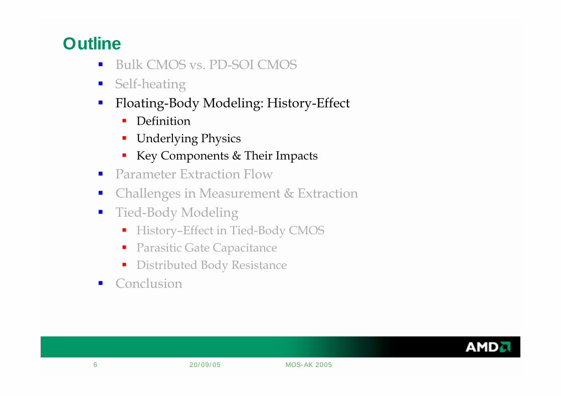
Outline! Bulk CMOS vs. PD-SOI CMOS! Self-heating! Floating-Body Modeling: History-Effect
! Definition! Underlying Physics! Key Components & Their Impacts
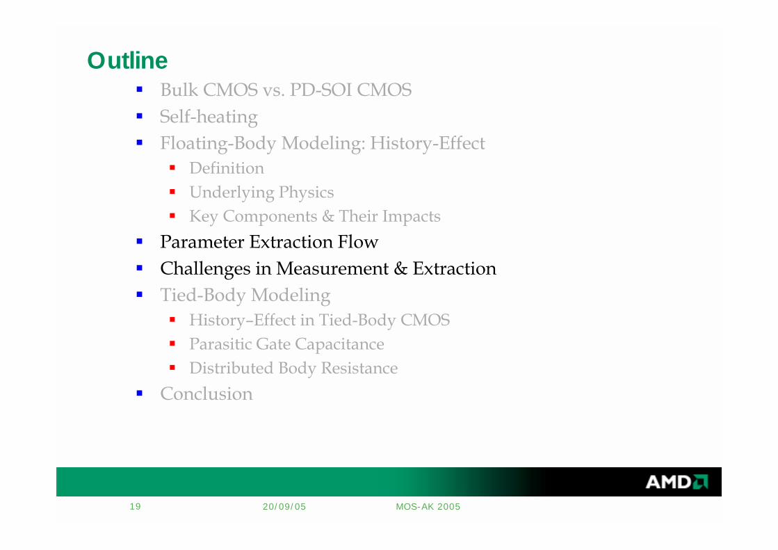
! Parameter Extraction Flow! Challenges in Measurement & Extraction! Tied-Body Modeling
! History–Effect in Tied-Body CMOS! Parasitic Gate Capacitance! Distributed Body Resistance
! Conclusion

20/09/05 MOS-AK 20053
Outline! Bulk CMOS vs. PD-SOI CMOS! Self-heating! Floating-Body Modeling: History-Effect
! Definition! Underlying Physics! Key Components & Their Impacts
! Parameter Extraction Flow! Challenges in Measurement & Extraction! Tied-Body Modeling
! History–Effect in Tied-Body CMOS! Parasitic Gate Capacitance! Distributed Body Resistance
! Conclusion

20/09/05 MOS-AK 20054
Bulk CMOS vs. PD-SOI CMOS
! The chief difference of the PD-SOI is that the body of each SOI transistor is an independent 4th terminal for the device
! When absolutely needed, the body can be fixed to a chosen potential with a body tie:
! However, in 99.9% of the chip, transistors will be operating as floating body devices
Bulk CMOS
Identical body potential
PD-SOI CMOS
Floating Body
Transistor
Transistorwith body tie
Floating Body
Transistor
Transistorwith body tie
Independent body potential

20/09/05 MOS-AK 20055
Self-Heating
! Thermal conductivity! Ksi = 60 - 148W/mK! Kox = 0.2 - 1.2W/mK
! Relatively poor modeling! Occasional convergence issue
0 0.4 0.8 1.2 1.6 2Drain Voltage(V)
0
3E-4
6E-4
9E-4
1.2E-3
1.5E-3
Drai
nCu
rrent
(A/u
m)
without self-heating
with self-heating
Vgs=0.5 V
Vgs=1.0 V
Vgs=1.5 V
Vgs=2.0 V
0 0.4 0.8 1.2 1.6 2Drain Voltage(V)
0
3E-4
6E-4
9E-4
1.2E-3
1.5E-3
Drai
nCu
rrent
(A/u
m)
without self-heating
with self-heating
Vgs=0.5 V
Vgs=1.0 V
Vgs=1.5 V
Vgs=2.0 V
0 0.4 0.8 1.2 1.6 2Drain Voltage(V)
0
3E-4
6E-4
9E-4
1.2E-3
1.5E-3
Drai
nCu
rrent
(A/u
m)
without self-heating
with self-heating
Vgs=0.5 V
Vgs=1.0 V
Vgs=1.5 V
Vgs=2.0 V
PowerRthCth
20/09/05 MOS-AK 20056
Outline! Bulk CMOS vs. PD-SOI CMOS! Self-heating! Floating-Body Modeling: History-Effect
! Definition! Underlying Physics! Key Components & Their Impacts
! Parameter Extraction Flow! Challenges in Measurement & Extraction! Tied-Body Modeling
! History–Effect in Tied-Body CMOS! Parasitic Gate Capacitance! Distributed Body Resistance
! Conclusion

20/09/05 MOS-AK 20057
CMOS Inverter Operation

20/09/05 MOS-AK 20058
Definition of History-Effect
! 1st switch: input transition after being held constant for a long time.! 2nd switch: input transition short time after the 1st switch.
τ 1st
τ 2nd
History-effectH = (τ 1st – τ 2nd) / τ 2nd
20/09/05 MOS-AK 20059
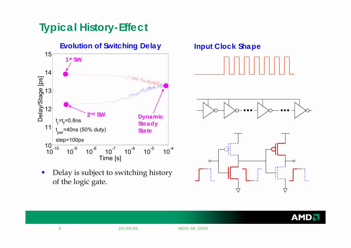
Typical History-Effect
! Delay is subject to switching history of the logic gate.
Input Clock Shape
Dynamic Steady State
2nd SW
1st SW
10-10
10-9
10-8
10-7
10-6
10-5
10-410
11
12
13
14
15
Time [s]
Del
ay/S
tage
[ps]
tr=tf=0.8ns
tper=40ns (50% duty)
step=100ps
Evolution of Switching Delay

20/09/05 MOS-AK 200510
What Causes History-Effect?
! Body Potential is a function of:! Capacitive coupling to
! Source! Drain! Gate! Substrate (small)
! Diode Leakages to! Source! Drain
! Gate Leakage! Impact Ionization
! Also subject to the previous switching history
Source Drain
Substrate
Buried Oxide

20/09/05 MOS-AK 200511
Combined Capacitive/Resistive Network
R1C1
R2C2
Time
Vol
tage
R-Divider
C-Divider
RC Decay

20/09/05 MOS-AK 200512
Time for Actual Contribution to Speed
! 1st SW : Initial DC! 2nd SW : Initial DC + Capacitive Coupling
Capacitive Coupling
Initial DCConditions

20/09/05 MOS-AK 200513
Capacitive Coupling
! Capacitive coupling is stronger to drain than to gate.
Gate Coupling
Drain Coupling
Gate Coupling
Drain Coupling

20/09/05 MOS-AK 200514
Key Components (Initial DC Condition)
! 1st SW Initial! KCL balance between forward and reverse Idiode
! Accumulation Igb is much smaller than forward Idiode
! 2nd SW Initial! KCL balance between forward Idiode*2 and inversion Igb
1st SW1st SW
Idio,revIdio,rev
Idio,forIdio,for
Igb,accIgb,acc
Igb,invIgb,inv
2nd SW2nd SW
Idio,forIdio,for

20/09/05 MOS-AK 200515
Key Components (AC Coupling)
! Basically a voltage-divider that consists of:! gate-body capacitance and junction capacitance
! Drain AC coupling is more significant than gate AC coupling
revjforjaccgb
revjDDbs CCC
CVV
,,,
,
++=∆
Cj,forCj,for
Cj,revCj,rev
Cgb,accCgb,acc
VDDVDD
+
∆Vb-
+
∆Vb-
20/09/05 MOS-AK 200516
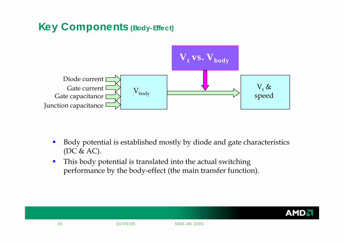
Key Components (Body-Effect)
! Body potential is established mostly by diode and gate characteristics (DC & AC).
! This body potential is translated into the actual switching performance by the body-effect (the main transfer function).
Vbody
Vt vs. Vbody
Vt & speed
Diode currentGate current
Gate capacitanceJunction capacitance

20/09/05 MOS-AK 200517
Impact of Gate Capacitance & Current
! Cgb is critical for VDD dependence slope! Igb is a major factor in 130nm technology and below
Increasing inversion Igb
2nd Vb ↑
0.8 1.0 1.2 1.4 1.6-10
-5
0
5
10
15
20
25
30
(1st-2
nd)/2
nd [%
]
VDD [V]
Inversion Igb ImpactInversion Cgb Impact
0.8 1.0 1.2 1.4 1.6-10
-5
0
5
10
15
20
25
30
(1st-2
nd)/2
nd [%
]
VDD [V]
Increasing accumulation Cgb
2nd Vb ↓
dbsbgb
dbDDndb CCC
CVV++
=∆ 2,

20/09/05 MOS-AK 200518
Impact of Diode Current
! The diode current characteristic is the key characteristic dominating the VDDand temperature dependences of the history-effect:! Proportional to forward Idiode! Inversely proportional to reverse Idiode
Increasing forward Idiode
1st Vb ↓↓ 2nd Vb ↓
Forward Idiode Level Impact
0.8 1.0 1.2 1.4 1.6-10
-5
0
5
10
15
20
25
30
(1st-2
nd)/2
nd [%
]
VDD [V]
Reverse Idiode Impact
0.8 1.0 1.2 1.4 1.6-10
-5
0
5
10
15
20
25
30
(1st-2
nd)/2
nd [%
]
VDD [V]
Increasing reverse Idiode
1st Vb ↑
20/09/05 MOS-AK 200519
Outline! Bulk CMOS vs. PD-SOI CMOS! Self-heating! Floating-Body Modeling: History-Effect
! Definition! Underlying Physics! Key Components & Their Impacts
! Parameter Extraction Flow! Challenges in Measurement & Extraction! Tied-Body Modeling
! History–Effect in Tied-Body CMOS! Parasitic Gate Capacitance! Distributed Body Resistance
! Conclusion
20/09/05 MOS-AK 200520
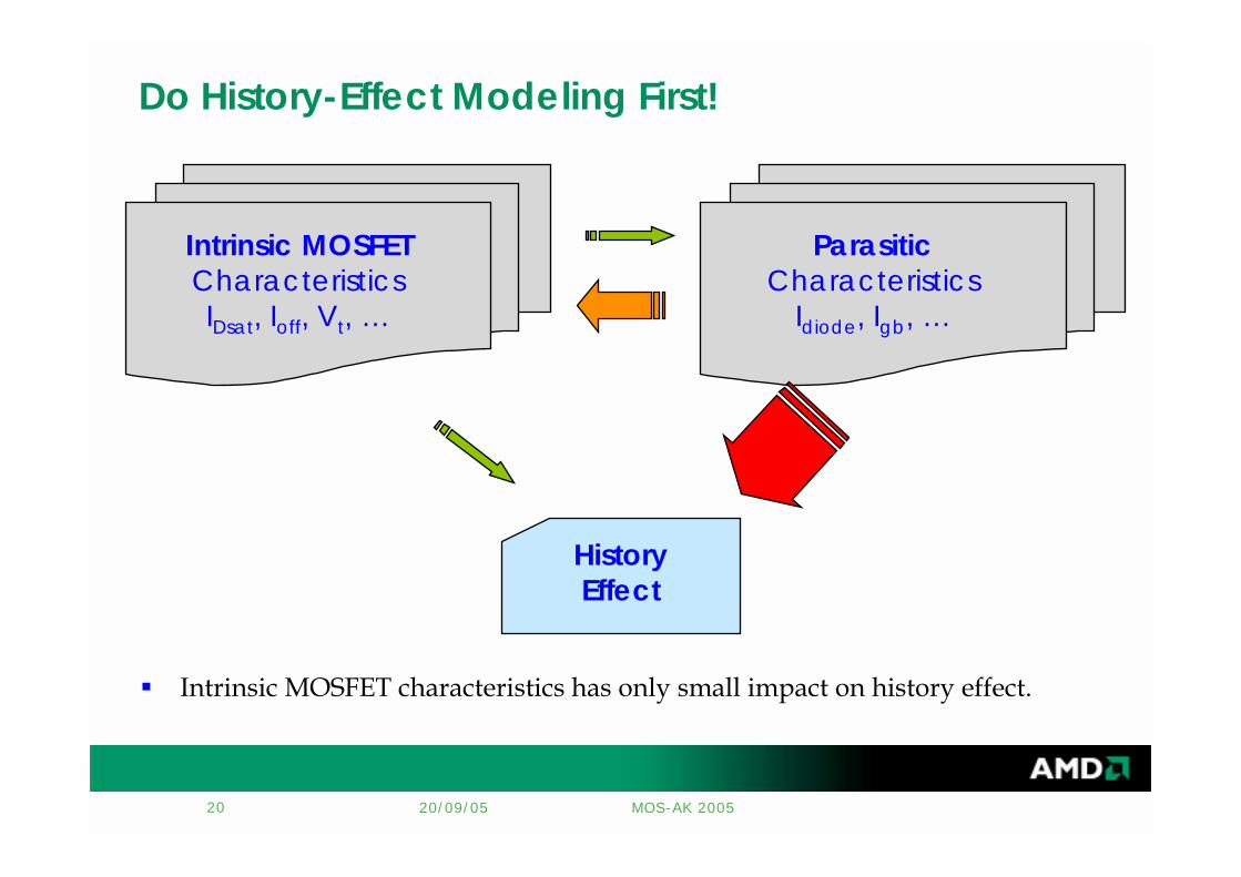
Do History-Effect Modeling First!
! Intrinsic MOSFET characteristics has only small impact on history effect.
Intrinsic MOSFETCharacteristicsIDsat, Ioff, Vt, …
ParasiticCharacteristics
Idiode, Igb, …
History Effect

20/09/05 MOS-AK 200521
PD-SOI Parameter Extraction Procedure
Body-Effect & Cg Fitting
Very Crude IV Fitting
Body Currents Fitting(Idiode, Igb, etc)
CheckHistory Effect
Refine All IV Fitting
TiedBody
FloatingBody

20/09/05 MOS-AK 200522
Challenges in Measurement & Extraction
Active
Gate Poly
P+ I/I
STI
P+ N+
P+ P- P w/ halo
Parasitic Opposite
Type Gate
Neck Easily Gets Fully-Depleted
20/09/05 MOS-AK 200523
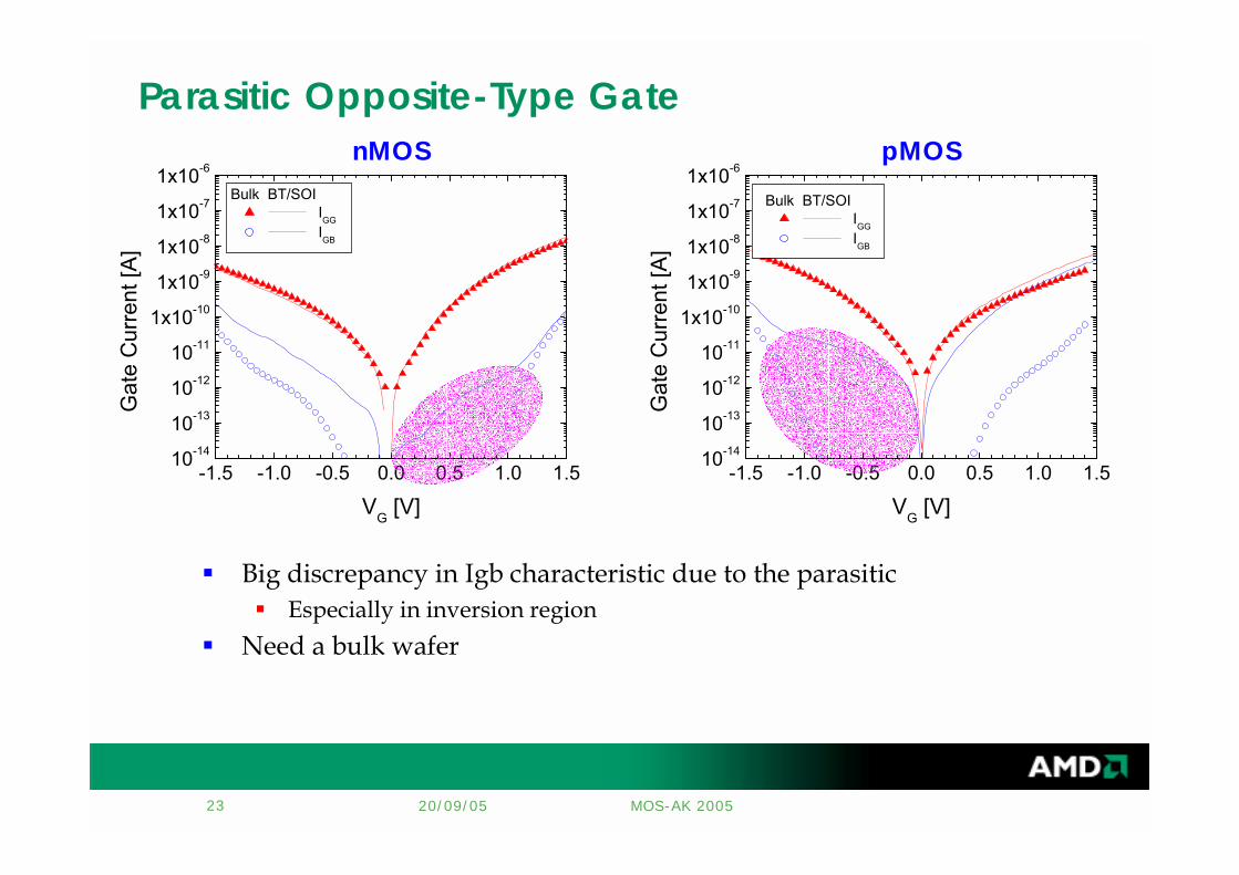
Parasitic Opposite-Type Gate
! Big discrepancy in Igb characteristic due to the parasitic ! Especially in inversion region
! Need a bulk wafer
-1.5 -1.0 -0.5 0.0 0.5 1.0 1.510-14
10-13
10-12
10-11
1x10⁻¹⁰
1x10⁻⁹
1x10⁻⁸
1x10⁻⁷
1x10⁻⁶
Bulk BT/SOI IGG IGB
Gat
e C
urre
nt [A
]
VG [V]
pMOS
-1.5 -1.0 -0.5 0.0 0.5 1.0 1.510-14
10-13
10-12
10-11
1x10⁻¹⁰
1x10⁻⁹
1x10⁻⁸
1x10⁻⁷
1x10⁻⁶
Bulk BT/SOI IGG IGB
Gat
e C
urre
nt [A
]
VG [V]
nMOS

20/09/05 MOS-AK 200524
Fully-Depleted Neck
! Low-doping neck can cause artifacts in measured data
-0.6 -0.4 -0.2 0.0 0.2 0.4 0.60.0
0.1
0.2
0.3
0.4
0.5
VDS=1.2V
VDS=0.1V
nMOSFET 2/0.0875µm
V T [V
]
Vbs [V]
Body-Effect
-1.0 -0.5 0.0 0.50.0
0.5
1.0
1.5
CJu
nctio
n [pF]
Vbias [V]
Junction Capacitance

20/09/05 MOS-AK 200525
Back-Bias Range of Interest
! Sometimes the body effect is not able to fit for the entire range.! Then some range should be compromised.! Separating TB and FB models maybe more desirable.
Tied Body & Bulk
Floating Body
-0.6 -0.4 -0.2 0.0 0.2 0.4 0.60.0
0.1
0.2
0.3
0.4
0.5
VDS=1.2V
VDS=0.1V
nMOSFET 2/0.0875µm
V T [V
]
Vbs [V]
Reverse
Forward

20/09/05 MOS-AK 200526
Outline! Bulk CMOS vs. PD-SOI CMOS! Self-heating! Floating-Body Modeling: History-Effect
! Definition! Underlying Physics! Key Components & Their Impacts
! Parameter Extraction Flow! Challenges in Measurement & Extraction! Tied-Body Modeling
! History–Effect in Tied-Body CMOS! Parasitic Gate Capacitance! Distributed Body Resistance
! Conclusion

20/09/05 MOS-AK 200527
Can Body Be Really Tied?
! Tied-body PD-SOI circuit experiences the coupling effects exactly same as floating-body one.
! Thus it exhibits history effect too.
0.0 0.1 0.2 0.3 0.4 0.5-0.3
-0.2
-0.1
0.0
0.1
0.2
0.3
Vbo
dy [V
]
Time [nsec]
Body Potential Fluctuation
Gate Coupling
Drain Coupling
Body RC Decay
108 109 1010
0
4
8
12WN=WP/2=1µm
(1st-2
nd)/2
nd [%
]
Frequency [Hz]
History Effect of Tied-Body CMOS

20/09/05 MOS-AK 200528
BSIM-SOI: Gate Capacitance
Active
Gate Poly
P+ I/I Drain
Source
Body
An+Ap+
Physical
Drain
Source
Body
BSIM-SOI
Agbcp
Rbodyext Rbp
n+/pn+/p-p+/p-
Rbodyext Rbp
n+/pn+/p-p+/p-
Rbodyext Rbp
n+/p n+/p n+/p
Rbodyext Rbp
n+/p n+/p n+/p

20/09/05 MOS-AK 200529
1 2 3-3 -2 -1 0
VG [V]
CG
G
BSIM-SOI: Gate Capacitance
∫ ⋅≈ T
FB
V
V GSGGB dVCQ
N+ gateP body
P+ gateP body
Gate CapacitanceActive
Gate Poly
P+ I/I
STI
P+ N+
P+ P- P w/ halo
∫ ⋅≈DD
T
V
V GSGGC dVCQOver-
Estimated

20/09/05 MOS-AK 200530
BSIM-SOI: Gate Capacitance
108 109 10106
7
8
9
WN=WP/2=1µm10 FET Segments
Physical Agbcp=An++Ap+ Agbcp=An+ Agbcp=An++Ap+/3
Del
ay (1
st+2
nd)/2
[ps/
stag
e]
Frequency [Hz]
Impact on Switching Delay
0 1 2 30
10
20
30
40
Qp+ Qn+ Qp+/Qn+ Ratio
VG [V]
QG
C
0.0
0.2
0.4
0.6
0.8
Qp+
/Qn+
Charge Ratio
~4.5%
! The charge ratio is 0.2~0.5 within practical range! 2 ~ 5x overestimation
! Its impact of switching delay is not negligible

20/09/05 MOS-AK 200531
BSIM-SOI: Distributed Body ResistanceSingle LumpedDistributed
Rbodyext RbpH/N
n+/pFET
n+/p-cap
p+/p-cap
n+/pFET
RbpH/N
N segments
Rbodyext Rbp
ModelMeasurement
DC Values AC Values?

20/09/05 MOS-AK 200532
BSIM-SOI: Distributed Body Resistance
108 109 1010
0
2
4
6
8
10
WN=WP/2=5µm
WN=WP/2=1µm
Agbcp=An++Ap+/3 Physical 1-Lump Scale=1.0 1-Lump Scale=1/3 1-Lump Scale=0.1
(1st-2
nd)/2
nd [%
]
Frequency [Hz]
Rule of Thumb! Factor of 1/3 for single-side contact; 1/12 for double-side contact! Mathematically derived for gate resistance noise
! R. P. Jinal, IEEE T-ED, pp. 1505-1509, October 1984! Applicable for other distributed resistance associated with active gain
108 109 1010
0
2
4
6
8
10
WN=WP/2=5µm
WN=WP/2=1µm
Agbcp=An++Ap+/3Rbodyext=10KΩ
Physical 1-Lump Scale=1.0 1-Lump Scale=1/3 1-Lump Scale=1/12
(1st-2
nd)/2
nd [%
]
Frequency [Hz]
Double-Side (H-Gate)Single-Side (T-Gate)

20/09/05 MOS-AK 200533
Conclusion! Self-heating is poorly modeled in general and worsens the
convergence! History-effect is one of the major difficulties in floating-body PD-
SOI parameter extraction! It has to be taken care of in the early stage of extraction! Accurate measurement & extraction of key components are very tricky
and challenging! Tied-body PD-SOI parameters need to be carefully chosen for
BSIM-SOI model! Parasitic gate capacitance needs to be scaled! Body resistance should be scaled by 1/3 for single-side; 1/12 for
double-side
![Extraction of Palladium(II) from Hydrochloric Acid ... · extraction of Pd(II). The use of either TOPO or Aliquat 336 with LIX 63 improves the extraction of Pd(II) [16]. In our work](https://img.pdfslide.net/doc/110x75/5e2680d1126c377132412df2/extraction-of-palladiumii-from-hydrochloric-acid-extraction-of-pdii-the.jpg)