Embed Size (px)
Citation preview

A 14-BIT PSEUDO-DIFFERENTIAL CURRENT-SOURCE
RESISTOR-STRING HYBRID DIGITAL-TO-ANALOGUE
(DAC) CONVERTER WITH LOW POWER
CONSUMPTION
CHANG HUI YI
UNIVERSITI SAINS MALAYSIA
2017
brought to you by COREView metadata, citation and similar papers at core.ac.uk
provided by Repository@USM

A 14-BIT PSEUDO-DIFFERENTIAL CURRENT-SOURCE
RESISTOR-STRING HYBRID DIGITAL-TO-ANALOGUE
(DAC) CONVERTER WITH LOW POWER
CONSUMPTION
by
CHANG HUI YI
A Dissertation submitted for partial fulfillment of the requirements
for the degree of Master of Science
(Microelectronic Engineering)
AUGUST 2017

ii
ACKNOWLEDGEMENTS
First of all, I thank God for His never-ending love and grace upon this completion
of this dissertation. God is indeed all good, and the source of all strength and courage to
go through many problems in the entire duration of the project.
In this stipulated time, I would like to thank my parents for all their love and
spiritual guidance. I would like to thanks my parents in the bottom of my heart for their
supports. Both my dad and mom always provide me moral support by motivate me when
I faced problems with my project. In all adversaries, they are the cornerstone for me to
fall back on, and I really thanks them from the deepest of my heart.
I would also like to send my high gratitude of gratefulness to my supervisor, Dr.
Mohamed Fauzi Packeer Mohamed. Without his guidance and knowledge, this project
would not be success. He ensure the concept and knowledge assigns to me is clear and
easy to understand. He will help me every time I faced difficulties throughout the duration
of the project. On top of that, I would like to acknowledge for the lavish support and
cooperation to all USM’s staffs, and technicians.
Last but certainly not the least, I would like to thank my friends for being together
and fight on for the success of the project. Their lending hands were just in time whenever
I had problems on my project. They provided their precious opinion and advices on my
project from the beginning of the semester. Thank you all for the help.

iii
TABLE OF CONTENTS
ACKNOWLEDGEMENTS ........................................................................................... ii
TABLE OF CONTENTS .............................................................................................. iii
LIST OF TABLES ....................................................................................................... viii
LIST OF FIGURES ....................................................................................................... ix
LIST OF SYMBOLS AND ABBREVIATIONS ......................................................... xi
ABSTRAK ..................................................................................................................... xii
ABSTRACT .................................................................................................................. xiii
CHAPTER 1 .................................................................................................................... 1
1.1 Background ........................................................................................................... 1
1.2 Problem Statement ................................................................................................ 3
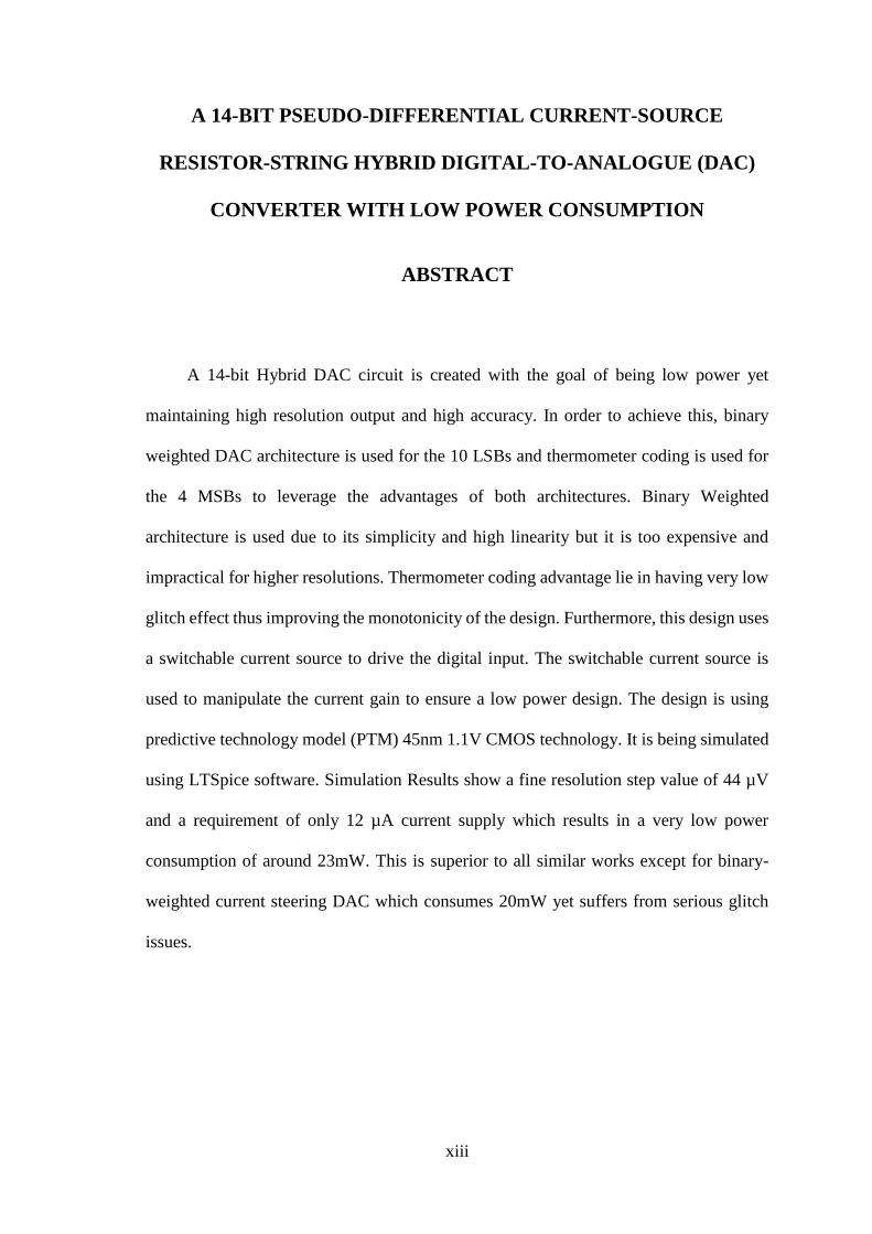
1.3 Research Objectives .............................................................................................. 5
1.4 Scope of Research ................................................................................................. 5
1.5 Outline of Report .................................................................................................. 6
CHAPTER 2 .................................................................................................................... 8
2.1 Overview ............................................................................................................... 8
2.2 Key Performance Aspects ..................................................................................... 9
2.2.1 Resolution .................................................................................................... 9
2.2.2 Integral Non-Linearity and Differential Non-Linearity ............................. 10
2.2.3 Circuit Complexity .................................................................................... 10

iv
2.2.4 Sampling Rate ........................................................................................... 11
2.2.5 Area ........................................................................................................... 11
2.2.6 Power ......................................................................................................... 11
2.3 Types of DAC ..................................................................................................... 12
2.3.1 Pulse-Width Modulator DAC .................................................................... 12
2.3.2 Over-Sampling DAC ................................................................................. 12
2.3.3 Binary Weighted Resistor DAC ................................................................ 13
2.3.3.1 R-2R Ladder DAC .......................................................................... 15
2.3.4 Current Steering DAC ............................................................................... 17
2.3.4.1 Binary Weighted Current DAC ...................................................... 18
2.3.4.2 Thermometer Coding DAC ............................................................ 20
2.4 Hybrid DAC Architecture System ...................................................................... 22
2.4.1 12-Bit Pseudo-Differential Hybrid DAC ................................................... 22
2.4.1.1 Switchable Current Source ............................................................. 24
2.4.1.2 Resistor String Circuit .................................................................... 25
2.4.1.3 Thermometer Coding ...................................................................... 26
2.4.1.4 MSB and LSB Segments of the 12-Bit Hybrid DAC .................... 27
2.5 DAC Blocks ........................................................................................................ 27
2.5.1 DAC Reference Blocks ............................................................................. 28
2.5.2 DAC Decoder ............................................................................................ 30
2.5.3 Single DAC ............................................................................................... 31
2.5.4 DAC Multiplexer ....................................................................................... 33

v
2.6 Summary ............................................................................................................. 34
CHAPTER 3 .................................................................................................................. 36
3.1 Overview ............................................................................................................. 36
3.2 Project Implementation Flow .............................................................................. 36
3.3 DAC Architecture Development ......................................................................... 39
3.3.1 Binary Weighted Resistor String Topology .............................................. 39
3.3.2 Thermometer Coded DAC Topology ........................................................ 45
3.3.3 Switchable Current Source ........................................................................ 47
3.3.4 Hybrid DAC .............................................................................................. 49
3.4 Parameters of 14-bits Hybrid DAC ..................................................................... 51
3.4.1 Parameters of Current Source ........................................................................ 53
3.4.2 Resistor Value for LSB DAC ........................................................................ 54
3.5 Analyses and Simulation of Hybrid DAC in LTSpice ........................................ 54
3.5.1 Power Measurement ...................................................................................... 55
3.6 Summary ............................................................................................................. 56
CHAPTER 4 .................................................................................................................. 58
4.1 Overview ............................................................................................................. 58
4.2 Theoretical Result for Power Consumption and Resolution ............................... 58
4.3 Simulation Result of DAC .................................................................................. 59
4.3.1 Different Resistor String Approach ........................................................... 60
4.3.2 Result of 14-Bit Hybrid DAC .................................................................... 62
vi
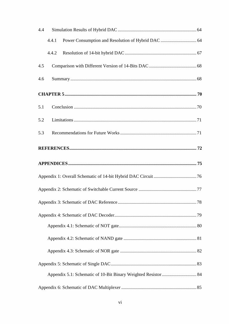
4.4 Simulation Results of Hybrid DAC .................................................................... 64
4.4.1 Power Consumption and Resolution of Hybrid DAC ............................... 64
4.4.2 Resolution of 14-bit hybrid DAC .............................................................. 67
4.5 Comparison with Different Version of 14-Bits DAC ......................................... 68
4.6 Summary ............................................................................................................. 68
CHAPTER 5 .................................................................................................................. 70
5.1 Conclusion .......................................................................................................... 70
5.2 Limitations .......................................................................................................... 71
5.3 Recommendations for Future Works .................................................................. 71
REFERENCES .............................................................................................................. 72
APPENDICES ............................................................................................................... 75
Appendix 1: Overall Schematic of 14-bit Hybrid DAC Circuit ..................................... 76
Appendix 2: Schematic of Switchable Current Source .................................................. 77
Appendix 3: Schematic of DAC Reference .................................................................... 78
Appendix 4: Schematic of DAC Decoder ....................................................................... 79
Appendix 4.1: Schematic of NOT gate ................................................................... 80
Appendix 4.2: Schematic of NAND gate ............................................................... 81
Appendix 4.3: Schematic of NOR gate .................................................................. 82
Appendix 5: Schematic of Single DAC .......................................................................... 83
Appendix 5.1: Schematic of 10-Bit Binary Weighted Resistor .............................. 84
Appendix 6: Schematic of DAC Multiplexer ................................................................. 85

vii
Appendix 6.1: Schematic of DAC Multiplexer Switch .......................................... 86

viii
LIST OF TABLES
Table 2.1: Operation mode of DAC multiplexer. ....................................................... 33
Table 3.1: Output voltage for 3-bits binary weighted resistor. ................................ 41
Table 3.2: Resistance value of BWR version 1 and BWR version 2. ....................... 42
Table 3.3: Thermometer coding for 4-MSB segment. ............................................... 46
Table 3.4: Simulation parameter of 14-bit hybrid DAC. .......................................... 52
Table 3.5: Parameters of switchable current source. ................................................ 54
Table 4.1: Result of the full scale voltage. ................................................................... 62
Table 4.2: Output voltage value for each binary weighted bit. ................................ 65
Table 4.3: Maximum and minimum power consumption of 14-bit hybrid DAC. .. 66
Table 4.4: Result comparison of different versions of 14-bits DAC. ........................ 68

ix
LIST OF FIGURES
Figure 1.1: DAC transform the digital data into analog signal . ................................ 1
Figure 2.1: 3-bit binary-weighted resistor string . ..................................................... 14
Figure 2.2: R-2R ladder DAC . .................................................................................... 17
Figure 2.3: Binary-weighted current DAC . ............................................................... 20
Figure 2.4: Thermometer code based current DAC . ................................................ 21
Figure 2.5: 12-bit pseudo-differential hybrid DAC architecture . ........................... 23
Figure 2.6: Switchable current source . ...................................................................... 24
Figure 2.7: Schematic drawing of binary-weighted resistor string . ........................ 25
Figure 2.8: MSB (top) and LSB (below) segments of the 12-bit hybrid DAC . ....... 28
Figure 2.9: DAC reference block diagram . ............................................................... 29
Figure 2.10: DAC decoder diagram . .......................................................................... 31
Figure 2.11: Single DAC block . .................................................................................. 32
Figure 2.12: DAC multiplexer diagram . .................................................................... 34
Figure 3.1: Overall design flow of 14-bit hybrid DAC. ............................................. 37
Figure 3.2: Specific project flow chart of 14-bit Hybrid DAC. ................................ 38
Figure 3.3: Simplified 3-bits binary weighted resistor circuit . ................................ 40
Figure 3.4: Binary weighted resistor version 1. ......................................................... 43
Figure 3.5: Binary weighted resistor version 2. ......................................................... 44
Figure 3.6: Block diagram of design current switch. ................................................. 48
Figure 3.7: Switchable current source. ....................................................................... 49
Figure 3.8: MSB and LSB segments of 14-bits hybrid DAC . .................................. 50
Figure 3.9: Input timing waveform for bit D0, D1 and D2. ...................................... 53
Figure 3.10: 3-bit DAC converter . .............................................................................. 55
Figure 3.11: Output current measurement for power consumption. ....................... 56

x
Figure 4.1: Result of 10-bit resistor string for (a) BWR version 1 and (b) BWR
version 2. ........................................................................................................................ 61
Figure 4. 2: Hybrid DAC result for (a) BWR version 1 and (b) BWR version 2. ... 63
Figure 4.3: Result of output current of the hybrid DAC .......................................... 66

xi
LIST OF SYMBOLS AND ABBREVIATIONS
DAC Digital-to-Analog Converter
DNL Differential Non-Linearity
INL Integral Non-Linearity
LSB Least Significant Bit
MSB Most Significant Bit
LTSpice Linear Technology Spice IV
PTM Predictive Technology Model
KPA Key Performance Aspects
dB Decibel
CMOS Complementary Metal Oxide Semiconductor
ADC Analog-To-Digital Converter
THD Total Harmonic Distortion
R-2R ladder Resistor Ladder Network
HBT Heterojunction Bipolar Transistor
SoC System-on-Chip
W/L Width-to-Length Ratio
Hz Hertz
W Watt
VDD Supply Voltage
GND Ground
PMOS Positive Channel Metal Oxide Semiconductor
SNR Signal-to-Noise Ratio

xii
SEBUAH 14-BIT PSEUDO-KEBEZAAN PUNCA-ARUS
RENTETAN-PERINTANG HIBRID PENUKAR DIGITAL KEPADA
ANALOG DENGAN PENGGUNAAN KUASA RENDAH
ABSTRAK
Sebuah 14-bit hibrid penukar digital-kepada-analog (DAC) diperbuat dengan
matlamat menggunakan kuasa rendah, tetapi mengekalkan keluaran resolusi tinggi dan
ketepatan. Untuk mencapai matlamat tersebut, seni bina DAC berwajaran binari
digunakan untuk 10 bit kepentingan paling rendah (LSB) dan pengekodan termometer
digunakan untuk 4 bit kepentingan paling tinggi (MSB) supaya memaksimakan kelebihan
daripada kedua-dua seni bina. Seni bina DAC berwajaran binari digunakan oleh kerana
sifat kesederhanaan dan kelinearan tetapi kos tinggi dan tidak praktikal untuk resolusi
tinggi. Oleh itu, pengekodan thermometer yang mempunyai glic yang rendah dan boleh
meningkatkan monotonicity reka bentuk tersebut digunakan. Selain itu, reka bentuk
projek ini menggunakan sumber arus boleh suis untuk memacu input digital. Sumber arus
boleh suis tersebut digunakan untuk memanipulasi gandaan arus untuk memastikan kuasa
rendah reka bentuk. Reka bentuk tersebut menggunakan model ramalan teknologi (PTM)
45nm 1.1V CMOS teknologi. Projek ini disimulasikan dengan perisian LTSpice.
Keputusan simulasi menunjukkan resolusi langkah halus 43.981µV dan keperluan arus
hanya 11.967 µA menyumbang kepada penggunaan kuasa yang sangat rendah sebanyak
23mW. Reka bentuk tersebut sesuai kepada semua kerja yang serupa selain daripada DAC
berwajaran binari yang menggunakan 20mW dan mempunyai isu glith.
xiii
A 14-BIT PSEUDO-DIFFERENTIAL CURRENT-SOURCE
RESISTOR-STRING HYBRID DIGITAL-TO-ANALOGUE (DAC)
CONVERTER WITH LOW POWER CONSUMPTION
ABSTRACT
A 14-bit Hybrid DAC circuit is created with the goal of being low power yet
maintaining high resolution output and high accuracy. In order to achieve this, binary
weighted DAC architecture is used for the 10 LSBs and thermometer coding is used for
the 4 MSBs to leverage the advantages of both architectures. Binary Weighted
architecture is used due to its simplicity and high linearity but it is too expensive and
impractical for higher resolutions. Thermometer coding advantage lie in having very low
glitch effect thus improving the monotonicity of the design. Furthermore, this design uses
a switchable current source to drive the digital input. The switchable current source is
used to manipulate the current gain to ensure a low power design. The design is using
predictive technology model (PTM) 45nm 1.1V CMOS technology. It is being simulated
using LTSpice software. Simulation Results show a fine resolution step value of 44 µV
and a requirement of only 12 µA current supply which results in a very low power
consumption of around 23mW. This is superior to all similar works except for binary-
weighted current steering DAC which consumes 20mW yet suffers from serious glitch
issues.

1
CHAPTER 1
INTRODUCTION
1.1 Background
Digital-to-analog converter (DAC) is a device that converts discrete bit values into
their matching continuously variable values [1]. The inputs are digital values of 0’s and
1’s with its discrete amplitude and time instants, whereas the analog outputs can be in
units of voltage or current [1]. Application of DAC can be easily found in most modern
electronics, such as music players, disc players, satellite digital decoders, communication
transmit channel and smart phone.
DAC is a fundamental application which covered the range from communication
up to the medical application. The most common example of DAC is to make the music
stored inside the player, which it is stored in digital bits, to be audible to the human ear.
DAC is crucial for sound amplification, as most of the audio devices, be it amplifiers or
speakers, can only deal with analog waveform [2].
Figure 1.1: DAC transform the digital data into analog signal [3].

2
Figure 1.1 illustrates how a DAC transforms the digital data into analog signal. The
blue arrows is the binary digital data, which has its own value in binary bits. These digital
values form a sound wave, as represented by the green line, when joined together by the
DAC. This explains the job of DAC, which is to reform the discrete digital values together
into a continuous analog waveform. It is very crucial to have enough arrows for maximum
representation of the shape, as well as having accurate dots. Horizontal X-axis represents
sampling time intervals, whereas vertical Y-axis represents the amplitude of the digital
value at that particular discrete time. The higher the number of dots on the X-axis, the
better the DAC as it can join back more dots to represent better analog shape. Good DAC
must also be able to sample accurate amplitude with minimal errors or glitch [3].
The need of a DAC comes from the necessity of storing analog voice signals, which
has a history of almost 50 years ago. Back then, an analog signal is stored as a groove on
a large black vinyl record. Signal inside is played on a player which has a needle which
moves back and forth. This will create an electrical analog signal representing the stored
sound [2]. In order to store music, the height of the analog signal is repeatedly sampled
and measured over time. It is then stored in a series of discrete binary bits on memory of
an audio device. These binary bits are digital audio signal. Digital music files are
performed using the form of Pulse Code Modulation (PCM), and are created by sampling
the amplitude of the analogue music signal at regular intervals. Digital audio data can be
stored in different compression formats, sampling rates, encoding methods and word size
[2].
From the above example, even gross over the years, the used of DAC still cannot
be eliminate or replace with any other technology. However, a conventional DAC have
its own weakness in term of resolution, accuracy, power consumption and many more
when the number of bit of a DAC is increasing. As important as storing the digital audio

3
bits, DAC is needed to convert its binary form back to the original audio analog signal,
as accurate as possible [2]. The device responsible for this conversion is none other than
DAC [2]. Thus, an improvement on the conventional DAC become valuable. Hybrid
DAC is the mixture creation based on the conventional DAC. The value of the hybrid
DAC is it will minimize the weakness of each conventional DAC and give a desire
outcomes when it is integrated into an application.
In the modern trend of the market, consumers are pampered with new technology
and looking forward for a device integrated with DAC to have a high resolution and low
power consumption. For the reasons given above, a hybrid DAC will definitely bring a
benefit to the industry.
1.2 Problem Statement
Power consumption and resolution in DAC go hand in hand as major issues focused
by DAC designers. High power consumption of a circuit will leads to glitches and give
the impact to the performance of a DAC in monotonicity and linearity, such as differential
non-linearity (DNL) and integral non-linearity (INL). In another word, a low power
consumption circuit will indirectly reduce the glitches. In order to achieve higher
resolution of a DAC, number of bits N of a DAC is playing the most important role.
Theoretically, when the number of bit is increasing, the voltage needed for the circuit will
also increasing. In another words, low power consumption and higher resolution are
opposed each other. As an answer to the arguments above, a 14-bits hybrid DAC is
proposed because it leverage the both factors at a balanced point. Furthermore, 14-bits
hybrid DAC is proposed because it still having market value due to some applications

4
such as music players, ultrasound communication transmit channel still need a 14-bits
DAC, but not 13-bit nor 15-bits DAC.
A 14-bits hybrid DAC is having a bit depth of 16384 transition points. Amplitude
or bit depth is simply refers to the resolution available to store the amplitude data. At this
point, definitely there is an argument of using 16-bits or higher in order to achieve a better
resolution. For a higher bit definitely will gives a higher resolution, but there is a
limitation where the DAC with higher bit will give a higher signal-to-noise ratio (SNR)
and impact the accuracy of the DAC.
Furthermore, especially in music players where it is the most common application
for DAC, higher bit depth exceeded 14-bits will always sound the same to the human ears
because there is a limit on the resolution that can be distinguish by human’s ears.
Additionally, the music players such as Apple have taken a step backwards in term of
capacity because they realize that the higher bits with higher resolution with no audible
improvement in quality is simply waste of resources.
After the consideration of the above factors, 14-bits hybrid DAC can give a golden
balanced points that achieves the ultimate utilization of resources to produce profoundly
high quality DAC in term of all aspects. Also, a hybrid type of DAC will minimize the
limitations of each conventional DAC and better fixed the demands of the market. A good
design is one that achieves the golden balance of utilizing the least resources to produce
the highest quality of output.
5
1.3 Research Objectives
The objectives of this project are:
1. To produce a 14-bit hybrid DAC with the architectures of binary-weighted resistor
and thermometer coded in order to get the most advantages of each type of DAC.
2. To produce a low power consumption hybrid DAC.
1.4 Scope of Research
The aim of the project is to produce a 14-bit hybrid DAC with the combination of
advantages of each algorithm and minimize the weakness of each conventional DAC.
This project is essentially an attempt to propose a low power consumption hybrid DAC
with higher resolution. With the combinational effect of binary weighted resistor and
thermometer coded in 10-bit least significant bit (LSB) and 4-bit most significant bit
(MSB) respectively, this could optimize the performance and power consumption. This
hybrid architecture is expected to achieve a high resolution and low power consumption.
The aforementioned hybrid DAC was implemented by using Linear Technology
Spice IV (LTSpice) software. The hybrid DAC architecture is presented with the
Predictive Technology Model (PTM) 45 nm 1.1V CMOS process technology. A 45 nm
technology is chosen for this project due to the maturity of the tools and the model file
available best fit the project. An appropriate technology used is one of the important factor
to help in reduce the power consumption where the smaller the technology, the power
needed by the transistors also will be lower.
Simulations are performed and verified with the LTSpice software. For ease of
study and troubleshooting, the overall circuit is divided into a few blocks of circuit, such
as voltage reference, digital decoder and many more. This architecture is expected to give

6
an output voltage within 1.1 V – 0 V. The supply voltage is 1.1V which is fixed in current
design. Besides, when migrating from different technology, the transistor width to length
ratio in the architecture will need to be redesign again.
1.5 Outline of Report
This report will consist of five main chapters that explain the full details and
specifications from the beginning to the conclusion of this project.
Chapter 2 is about literature reviews on previous DAC architectures and
techniques. The main sources of literature are from conference proceedings, engineering
journals and online reliable resources. Each DAC architecture is discussed briefly in terms
of reliability, speed, power consumption and glitch. Some hybrid DAC implementations
are discussed in brief in their respective concepts and methods. The methods discussed
here are compared and reviewed in their theoretical aspects.
Chapter 3 describes the development of 14-bit hybrid DAC. The process flow,
designs, and methods used to achieve the desired objectives are discussed in detail. The
means to carry out the simulation and collecting data are also discussed in detail. In
addition, the methods to evaluate the performance of the DAC are discussed in detail in
plotting the relevant values in a detailed graph.
Chapter 4 consists of tabulated data and analysis of the results of all simulations
of the project. All simulation results of the low power driver hybrid DAC is evaluated
and analyzed using a set of pre-determined data. The data consists of many types of
signals to be fed into the hybrid DAC. In doing so, the performances of the hybrid DAC
can be tested in the simulation against all possible scenarios.

7
Chapter 5 summarizes the entire project whether the objective is fulfilled. A brief
conclusion based on the observations and results is discussed here. Recommendations of
any future work on this field are made here.

8
CHAPTER 2
LITERATURE REVIEW
2.1 Overview
DACs are used to convert the digital data sequence to analogue signal waveforms.
Over the years, many conventional DAC architectures had been developed such as pulse-
width modulator DAC, over-sampling DAC, weighted current-steering, resistor ladder
network (R-2R ladder DAC), thermometer-coded DAC, and binary-weighted. Each of
these conventional DAC architecture has its benefits, flaws, and limitations. Each of the
conventional DAC differs in limitations in static and dynamic performance, including
linearity, monotonicity and glitch energy. In view of the limitations inhibited by the
conventional DACs, the hybrid DAC architecture is developed. This is to synergize and
leverage most of the advantages and least of the disadvantages from the conventional
DAC architectures.
This chapter will begin by explaining key performance aspects that are used to
evaluate various DAC architectures. It will then discuss several of the past hybrid DAC
proposed by previous researchers. All mentioned hybrid DACs are evaluated and
compared in terms of power consumption, glitch analysis and conversion accuracy. This
serves an important point to research their respective work to gain critical insights and
knowledge to achieve the project objectives. Based from their researches, a better and
more efficient DAC architecture system can be developed and implemented.
From the past researches, there are few techniques have been developed to tackle
the various error sources in DAC. In the era of nanometer technology, any small changes
in the physical factors can give a significant impact towards the performance of the device
build. Thus, the hybrid DAC architecture is developed by using PTM. The predictive

9
model is used for circuit characterization by giving the first eyesight of the design build.
This predictive model take in count every aspects such as the process variations, the
technologies used and the physical correlations among model parameters to give out an
accurate predict characteristics of nanoscale of complementary metal oxide
semiconductor (CMOS) [4].
2.2 Key Performance Aspects
There are various aspects that are used to evaluate the quality of design of a DAC
which called as Key Performance aspects (KPA). These KPAs vary from one application
to another. For example, to evaluate a DAC for audio applications, having a high
resolution would be of paramount importance while having low power or being able to
operate at high frequency has little importance. On the other hand, if a DAC is used for
communication applications being able to operate at high frequency would be of utmost
importance. Here is a list of the most important DAC KPA that will be discussed in this
chapter.
2.2.1 Resolution
The simplest KPA is the resolution of the DAC which can be easily represented by
the number of bits of the digital input to the DAC. While it is true that the higher the
number of bits the higher the resolution of the DAC, this always comes at the cost of
increased area, circuit complexity and power consumption. Certain applications have no
use of a very fine resolution. For example, power applications do not gain any advantages
from having a fine resolution. DACs used in power applications are more concerned by

10
low error margins (INL & DNL) as they tend to control very high voltages so accuracy is
of utmost importance.
2.2.2 Integral Non-Linearity and Differential Non-Linearity
INL and DNL are the basic parameters used to judge the accuracy of DAC. INL is
defined as the difference between the output voltages at step N versus the expected ideal
output value of the reference line at that point. While the DNL is the difference between
the actual increment height of transition N and the ideal increment value. Both of these
values are the key component of measuring the accuracy of a DAC. Vishva et al [5]
demonstrates the core difference between DNL and INL by comparing two simple yet
very commonly used DAC architectures. Accuracy is very crucial for critical applications
like power applications or various instrumentation control systems. Li at al [6] used a
combination of tricks to manage to eliminate the bottle neck created by glitches due to
non-linear distortions. This enabled them to create a design that can run at a 250 MS/s.
This demonstrates the design advantages of a carefully designed hybrid DAC in
overcoming INL and DNL limits.
2.2.3 Circuit Complexity
Circuit complexity is indeed an important aspect of a DAC. There is no value
gained of over designing a DAC for a certain application when a much simpler circuit has
the ability to perform equally if well designed. The more complex a circuit the more area
it requires and probably the higher power it will consume. That is why in some cases
sacrificing other KPAs happens to simplify the circuit.

11
2.2.4 Sampling Rate
Sampling rate is an important aspect of producing fine output. It is a measurement
of how fast a DAC respond to changing inputs. This is very important for
telecommunication and high speed applications. Nonetheless, creating a DAC that can
have a high sampling rate often faces serious bottle necks in the design such as increased
glitch and increased power consumption. Many creative designs have managed to achieve
high sampling rate. Zhang et al [7], approach which uses a 5 plus 9 segment PMOS
managed to achieve a clock frequency of 2.5 GHZ and only 40 db noise at 1 GHZ.
2.2.5 Area
Nowadays with circuits being smaller and smaller and handheld devices being more
and more powerful, circuit area matters significantly for DAC for applications involving
small devices like hand phones and tablets. Moreover, industrial and military applications
require powerful DACs to be fitted on minute devices and yet maintain very high
accuracy and performance. As mentioned above, circuit area is well connected to circuit
complexity, the lower the complexity, the smaller the area. Bringas et al [8] is a great
example of how a good design could create powerful DAC with small area. They made a
10-bits DAC using a hybrid of current steering for the LSB thermometer coding for the
MSB which created a design with great linearity yet using simple concepts and hence
smaller area.
2.2.6 Power
Power dissipation of a DAC is crucial for applications where the DAC is going to
be powered by battery or solar energy. It is very important for the DAC to consume less

12
power to be able to serve these applications. One topology that is known to be a good
balance of power is thermometer coding which saves power even as an ADC as
demonstrated by Ashwini et al [9].
2.3 Types of DAC
In development over the decades, there are many types of DAC have been develop
to meet the requirements of the endless application. In below segment discusses most
usual type of DACs which can be used in hybrid architectures.
2.3.1 Pulse-Width Modulator DAC
This is the lowest cost DAC. This DAC continuously switches a constant current or
voltage over a period of time. The duration of switching is determined by the binary input
code to the DAC. This type of DAC is mostly used in motor to control the speed, but it is
also applicable in other applications.
2.3.2 Over-Sampling DAC
Over-sampling DAC is based on interpolation. It means that this DAC converts
digital bits into analog signals by employing a strategy of pulse density conversion. There
are many advantages in going to this strategy. The main advantage is being able to
minimize the low internal resolution effect. The DAC operates using Delta-Sigma
Technology that encodes analog signals into digital signal by utilizing the same
methodology used by an analog-to-digital converter (ADC). Moreover, it has the ability
to transfer high bit-count low frequency digital signals into a lower bit-count with higher

13
frequency digital signals as part of the process to convert digital signals into analog which
is an important part of a DAC. These features make Oversampling DAC ideal for very
high resolution designs, for instance, those greater than 16 bits because of its high
linearity yet low cost. Furthermore, quantization results in a further mitigation of noise as
a result of the oversampling rate performance requirement of low-pass filter at the output.
With delta-sigma method sampling rate up-to 100,000 sample/s a resolution of 24 bits
can be obtained [1].
Normally, Oversampled DACs are the only solution for audio codecs, which require
dynamic range in excess of 16 bit, total harmonic distortion or THD in excess of 80 dB.
For this reason, audio cases are presented and studied in detail. Finally, the recent CMOS-
scaled technologies perform at higher speed and thus the concepts of oversampled DACs
have been recently applied to larger bandwidth devices, indicating a future increase in
development of oversampled DACs [10].
2.3.3 Binary Weighted Resistor DAC
Binary-weighted resistor is the easiest and simplest form of DAC. This DAC is
made from resistors connected in a series topology. All resistors have the same resistance.
Hence, the only way to control the resistance value is to manipulate the number of
resistors being used. This means that as the digital signal increases, the resistance increase
significantly. This approach is most suitable for low-resolution designs that have a small
digital input value. It is very expensive and impractical to be used for high resolution
inputs. This is because a higher the resolution of the input needs a higher resistance value.
This translates to more resistors needed to be used and this requires a very large area [1].
Another disadvantage of using large resistance is that it results into a mismatch between

14
the transistors and hence will affect the linearity of the design. All factors considered, this
DAC is most suitable for building up to 8-bit input DAC.
Figure 2.1 is an example for a 3-bit binary weighted resistor string DAC structure.
This DAC is connected to a current source which use to control the input. To understand
the operation of the resistor, consider the scenario with inputs being of low value. In that
case, the current source will be turned ON and a fixed current, I which it will be conducted
through the series of resistors. As the input bits value increase, resistance value should
increase significantly [11].
Figure 2.1: 3-bit binary-weighted resistor string [12].
Based on Figure 2.1, the simplified 3-bit equation is [12]:
𝑉𝑜𝑢𝑡 = (22𝐷[2] + 21𝐷[1] + 20𝐷[0] )(𝐼 × 𝑅) (2.1)
According to Equation 2.1, current, I represents fixed current flow, R represent the
LSB resistance, D is the bit of input.

15
2.3.3.1 R-2R Ladder DAC
Resistor ladder network also known as R-2R ladder DAC which is another type of
binary-weighted DAC. The main unique feature is the repeated cascaded connection of
T-resistor R and 2R. This feature results in higher precision as the production of
equivalent matched resistors or current sources is much simpler. Moreover, the simplicity
of this configuration means it is much cheaper to implement. It performs using cyclic
ladder like the configuration of accurate resistor networks [1].
The functionality of this DAC can be explained as follows. A string of resistor
ladder implements the non-repetitive reference network. The challenges associated with
the large current ratio of a binary-weighted DAC are mitigated using R-2R resistor ladder
where all current sources have identical values. This results in the fact that the current
switch for each bit steers the same amount of current. The issue of current source
mismatch as a result of the large current ratio is avoided. A block diagram is shown in
Figure 2.2. In this setting, resistors generate the binary output levels. The best way to
understand the functionality of this setting is by examining the Norton equivalent circuit
of each stage [13]. For this topology, only a resistor ratio of 2:1 is required, hence further
reducing the impact of mismatch. If only unit-sized resistors are used, the matching can
be even further improved. To achieve the desired resolution, resistor process variation is
ideal for imposing the minimum resistor width needed.
While R-2R architecture does have its advantages, the fact that only a fraction of
the current is passed to the following stage means that a portion of the current is wasted
in the resistor ladder. As the resolution of the DAC increases, the amount of wasted
current increases and the efficiency decreases.

16
Besides from the obvious efficiency issues, this architecture also suffers from
strong glitches resulting from any mismatch between the delays of the data signals to the
current switches. In fact, the timing skew between the data lanes
is the main factor that limits the sampling speed of the DAC [14]. A research showed that
for a 6-bit 25 GS/s R-2R DAC, a timing skew of 3 ps results in a
5.8 LSB glitch when the MSB toggles. They designed two R-2R DACs: a 6-bit 32 GS/s
DAC [15] and a 6-bit 28 GS/s DAC [16]. Different methods were applied to address
timing skew. The 32 GS/s DAC uses only a half rate clock and performs double sampling
of the data to relax the timing constraint. The 28 GS/s DAC uses a full rate clock and
relies on matching the interconnect length to minimize timing skew between the data
lanes. For a more recent version of their DAC at 60 GS/s, they used the same layout
technique and demonstrated a clear four-level eye diagram at 60 GS/s [17]. All three
DACs used InP heterojunction bipolar transistor (HBT) technology with fT and fMAX of
175 GHz and 260 GHz [15], respectively and much less loss, semi-insulating substrate
than that of the commercially available CMOS processes.
Higher sampling frequencies exposes the drawback of timing skew between data
lanes. With flip-flops, the data can be retimed before reaching the current switch.
However, at higher frequencies, the timing margin of the flip-flop is reduced [14]. This
simply means that suppressing the timing skew of the input data becomes very
challenging.
As in the binary-weighted current DAC, the R-2R topology also does not require a
thermometer decoder, which simplifies circuit design. Moreover, since the output current
switches have the same size, the data buffers, retimes and clock buffers driving the current
switches can be identical for all the lanes as well. This simplifies the clock tree design,
which is the highest frequency block in the system [18].

17
Figure 2.2: R-2R ladder DAC [18].
2.3.4 Current Steering DAC
The current-steering DAC is implemented by manipulate the current value which
has a significant advantage on high speed design. Normally, the input bits of the DAC is
connected to switchable current-sources. The main advantage of the current-steering
possess is that it is significantly faster that then voltage switches approach. This is
explained by the fact that referenced current is not interrupted and significant voltage will
be visible only at the output but not across the switches [12]. Another benefit of this
approach is that a decoder is not required and hence it has a much lower circuit complexity
with faster operating speed [19]. However, the negative aspects of this approach are
mainly having a limitation on static and dynamic performance. This can be accounted to
current mismatch, process variation and glitch energy.

18
2.3.4.1 Binary Weighted Current DAC
This DAC is formed by using weighted current sources which are joined to a switch
that is manipulated by the digital inputs [19]. There are many advantages of using this
approach. Firstly, it is power efficient and it takes up small area. Secondly, no decoder is
required which reduces circuit complexity significantly and allows it to operate at higher
speeds [20]. Therefore, the current-steering switching method performs much faster than
the voltage-switching mechanism. Nonetheless, this setting suffers from poor
performance in the special case of all switches transit the state simultaneously [12]. In
addition to that, the current-steering DAC also has limitations in dynamic performance,
such as glitch energies and current mismatch due to process variation.
A simplified circuit diagram of a binary-weighted DAC is shown in Figure 2.3.
Input binary codes switch the binary-weighted current sources to a 50 Ω on-chip load
resistor and a 50 Ω off-chip termination resistor to generate the analog voltage output.
For high speed DACs, a 50 Ω output impedance is necessary to match with the input
termination of the measurement equipment, such as an oscilloscope or spectrum analyzer.
It is important to have proper termination for high speed DACs to avoid signal
degradation. From the diagram, the obvious advantage of this architecture is that it only
requires N current sources for an N-bit DAC. This can result in area and power savings
by having fewer data lanes, which reduces the number of buffers necessary to drive them.
This is very important for high speed DACs, because smaller area means smaller footprint
and less layout parasitic capacitance to drive. As the conversion rate of the DAC increases,
the bandwidth of the DAC becomes increasingly limited by the interconnect capacitance.
Example of DACs using binary-weighted current sources include a 6-bit, 20 GS/s DAC
[21].

19
When it comes to area and power savings, they are somewhat limited because the
current switches need to be scaled with the current to ensure the transistors are biased at
peak fT current density. As a result, all the buffers driving the current switches also
need to be scaled appropriately. This architecture is demanding in terms of device
matching to achieve high resolution. Sometimes, in order to reduce mismatch of the
current sources caused by the large ratio, it is desirable to use unit-sized current sources.
This results in an increase of the area of the DAC.
Having a large current ratio negatively impacts the dynamic performance of the
DAC. One of the researcher’s design [21], scaled buffers were used to drive the weighted
current sources. However, in order to save power, scaling was done such that there was
still a fan-out difference of 4:1 between the MSB and LSB. As a result, MSB lanes driving
a large load will have more delay, which will cause glitches at the DAC output. The
researcher[21] compensated for this delay by retiming the MSB earlier than the LSB.
Also, to further reduce the current ratio, they applied the LSB current to a 25 Ω load,
whereas the rest of the binary currents go to a 50 Ω load.
There are two disadvantages of a binary-weighted DAC that plague all DACs not
using thermometer decoding. The DAC may not be monotonic. A monotonic DAC is
the one where the output always increases with increasing input code [22]. The other
disadvantage is that the DAC may suffer from large glitch energy when the MSB toggles,
for example, when the code changes from 1000 to 0111 for a 4-bit DAC. This problem is
especially pronounced for high speed DACs, because the duration of the bit period can
be too short for the glitch to settle within one bit period. Hence, it is important to align
the digital bits to reduce the glitch energy as much as possible.

20
The main advantage of the binary-weighted DAC is its simplicity. It does not
require thermometer decoder, which can be challenging to design at very high speed with
low power. Some designs have taken advantage of this fact while minimizing the impact
of the glitches by using binary-weighted currents for the LSBs only [23].
Figure 2.3: Binary-weighted current DAC [18].
2.3.4.2 Thermometer Coding DAC
This DAC consists of a decoding circuit of binary to thermometer codes. For N-bit
of DAC needs 2𝑁 − 1 current source. As the digital code increases by one, the
thermometer decoded bits switch one more current source to the output. All the current
sources have the same current, so the current switches and the circuit driving the current
switches are also identical [18]. Each of the current source is used in controlling the
current flow through the DAC. The digital signal must be translated into the
corresponding thermometer code, which is consisting 2𝑁 − 1 bits in thermometer code

21
for N-bit of the digital inputs. This decoder will convert into 2𝑁 − 1 bits in thermometer
code for any N-bit of binary inputs. For example, for a 4 bits DAC, it will have 15
segments.
Figure 2.4 shows the thermometer coded DAC. This kind of DAC architecture has
the minimum glitch effect. Hence, it has significantly better DNL, and glitch and
monotonicity performances as compared to other DAC architectures. However, this high
precision DAC architecture needs a high cost to build due to its encoding circuits needed.
It is more preferable in low resolution cases since the encoding circuit in high resolution
cases could be very large as the binary input bits is increasing [24].
Figure 2.4: Thermometer code based current DAC [18].

22
2.4 Hybrid DAC Architecture System
Hybrid DAC architecture is composed by integrating two or more type of
conventional DAC architectures as mentioned at section 2.2. In most integrated devices
where DACs are used, hybrid DAC is more preferred. This is because to provide a balance
among cost, speed and precision. To achieve this balance, using only any one of the
techniques mentioned above is very challenging.
It has to be pointed that the segmented DACs is special kind of hybrid DAC which
combines two principles. While for the most significant bits it employs the thermometer-
coded principle, and for the least significant bits, it utilizes the binary-weighted principle.
Via this hybrid methodology, a tradeoff is achieved in between the precision of the DAC
and the number of current sources required by the DAC.
2.4.1 12-Bit Pseudo-Differential Hybrid DAC
Figure 2.5 shows the overall block diagram of a 12-bit pseudo-differential hybrid
DAC. Referring to a researcher [12], this hybrid DAC consists of three conventional
DACs, which are thermometer coding DAC, binary-weighted resistor DAC, and
weighted current-steering DAC.
This hybrid DAC utilized the advantages of these three DAC. To start, the binary
weighted resistor DAC is used to represent 8 LSBs. On the other hand, the thermometer
coding scheme is used to represent 4 MSBs. Other than that, to provide current to follow
through the resistors topology layout, this configuration uses current-steering as a
switchable current source. As essential cell in the hybrid DAC architecture, this is used
to generate current to the resistors. Based on all of that, the 12-bit pseudo-differential
hybrid DAC has compelling advantages across different segments. For example, it has

23
better DNL and INL, along with a reduced overall area and lower circuit complexity [12].
The hybrid DAC configuration is quite compact. It is possible to be utilized at numerous
mixed signal designs or system on chip (SoC) implementation.
Figure 2.5: 12-bit pseudo-differential hybrid DAC architecture [12].
Referring to Figure 2.5, it is clearly shows that DAC reference block is the core to
the overall design as it provides constant bias voltages to two DAC blocks. The DAC
Decoder decodes the 12-bit binary input into an appropriate code for both DACs
simultaneously. It then splits 8-bit binary-weighted resistor string in LSB section and 4-
bit to 15-bit of thermometer coding decoder in MSB section. A DAC blocks are composed
by switchable current sources and resistor string circuit as the essential cell in DAC block,
three PMOS transistors are used to create the switchable current source with different
width-to-length ratio (W/L). It is used to supply the resistor string with a fixed current

24
when it is switched on. Each of the block or elements used in this hybrid DAC will have
more discussion in section below.
2.4.1.1 Switchable Current Source
Figure 2.6 clearly shows the structure of the switchable current source that is created
using three PMOS transistors. Its operation is dependent on the voltage level of the input
at gate of M3. High voltage at M3 turns the transistor off, which in return switch on the
current source. This will make a fixed value of current flows to IOUT through transistor
M2. If a low voltage be applied at M3, the current source is switched off. In this case, M3
will be supplied by a fixed current from the transistor M1 to the ground, instead of IOUT.
The fourth terminal of the PMOS transistors is tied to VDD is connected to the fourth
terminal of the PMOS transistors [12].
Figure 2.6: Switchable current source [12].


![[Go Igo Baduk Weiqi] Yi Chang-Ho Selected Tesuji Problems - Vol 1](https://img.pdfslide.net/doc/110x75/54f4a2e74a7959f82d8b45bc/go-igo-baduk-weiqi-yi-chang-ho-selected-tesuji-problems-vol-1.jpg)