Embed Size (px)
Citation preview

Chaos, Communication and ConsciousnessModule PH19510
Lecture 8
Entering the Transistor Age

Overview
Metals, Insulators & Semiconductors The junction diode The bipolar transistor Planar Processing

Metals, Insulators and Semiconductors Metals
Overlap of valence & conduction bands empty states for electrons to move into conduction
Insulators Large gap between valence & conduction bands No free states No conduction
Semiconductors (Silicon, Germanium, GaAs etc) Small gap between valence & conduction bands Some free states some conduction – depends on impurities, temperature etc.


Column IIIB, IVB & VB
Column IIIB B, Al … 3 electrons in outer shell
Column IVB C, Si, Ge … 4 electrons in outer shell Diamond like crystal
Column VB N, P, As … 5 electrons in outer shell

Crystal structure of Silicon
Diamond like Tetrahedral bonds Hard Brittle

Intrinsic Semiconductor
2D representation of crystal lattice
Semiconductor All electrons paired Valence band filled No-conduction

n-Type Semiconductor
Electron donor impurity
Column V (As, P) Low concentration ≈1:108 Add ‘free’ electron Electron Movement conduction
As

p-Type Semiconductor
Electron acceptor impurity
Column III (Boron) Low concentration ≈1:108 Add ‘hole’ Hole Movement conduction
B

pn Junction
n-type & p-type junction Spare electrons from n-
type fill holes in p-type depletion region n-type –ve
depletion region shrinks forward bias (conduction)
n-type +ve depletion region grows reverse bias (no conduction)
n p
n p-ve +ve
n p -ve+ve

Point contact PNP junction
First Transistor 1947 Brattain, Bardeen & Shockley
Ge
p pn

NPN Bipolar Junction Transistor
Emitter at ground +ve voltage on collector Collector-Base reverse
biased no current Apply +ve voltage on
base Electrons pulled from
emitter into base Collector base depletion
region shrinks many electrons flow
from Emitter to Collector Amplification
n
n
p
Collector
Base
Emitter

Shockley and Silicon Valley
1955 Shockely leaves Bell Forms Shockley Semiconductor in Palo Alto, CA 12 keen young engineers ‘Difficult’ management style
1957 Staff leave (The Traitorous 8) & form Fairchild
Semiconductor

From Germanium to Silicon
Germanium rare but easier to refine Silicon Common
25.7% of earth crust Electric Arc refining
Silicon forms stable oxide Better electrical and mechanical properties
21900
2 COSiCSiO C
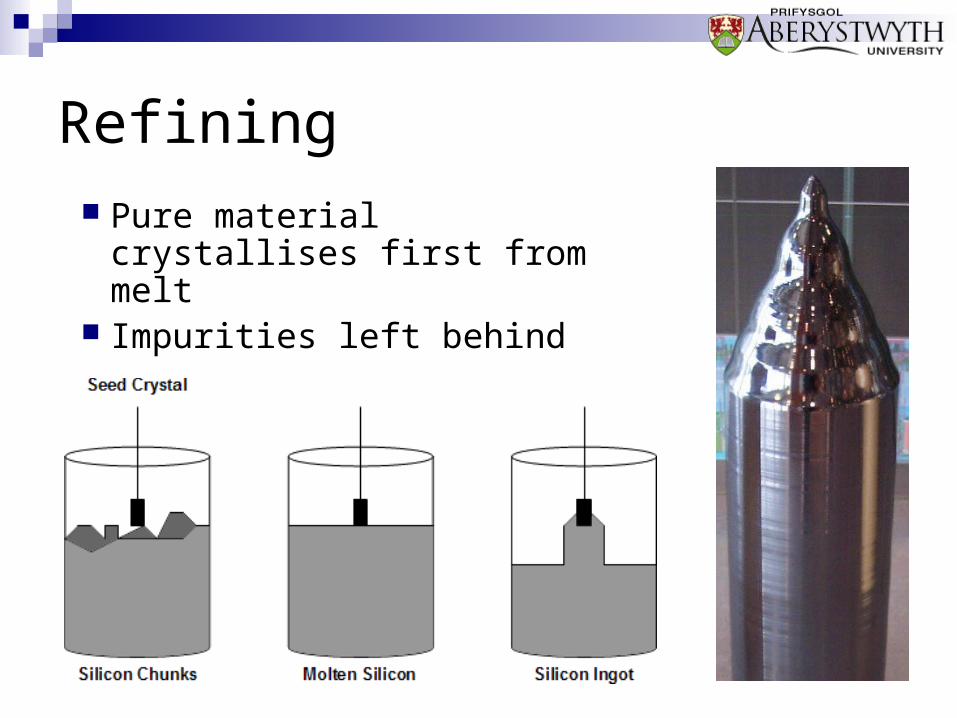
Refining
Pure material crystallises first from melt
Impurities left behind

Printing Transistors on Silicon
Planar process developed at Fairchild Possible to dope n-type so it becomes p-
type and vice versa Use of Silicon Dioxide (SiO2) as mask for
processing

Planar Transistors
n-Substrate Grow Oxide Pattern & etch oxide Diffuse p-dopant Grow Oxide Pattern & etch oxide Diffuse n-dopant Grow Oxide Pattern & etch oxide Metal Contactsn
CollectorBaseEmitter
Vertical Transistor

Review of Lecture 8
Metals, Insulators & Semiconductors The junction diode The bipolar transistor Planar Processing

ReferencesWhere to go for more Information inventors.about.com/library/weekly/aa061698.htm US Patent 2524035
www.eepatents.com/feature/2524035.html Intel Education programme
www.intel.com/education/transworks/ Principles of semiconductor devices
ece-www.colorado.edu/~bart/book/book/ Webelements.com The Britney Spears guide to Semiconductor Physics
britneyspears.ac/physics/basics/basics.htm - www.icknowledge.com