Embed Size (px)
DESCRIPTION
Chap 3. Simple Diode I-V Representation. Diode Symbols and Ckt Representation. Diode SPICE parameters. Simple Diode Rectifer. Limiters/Clippers. LOG COMPUTATION AND THE DIODE. COMPUTATION AND THE DIODE. Basic Semiconductor Concepts-Review. Basic Semiconductor Concepts. Doping Example. - PowerPoint PPT Presentation
Citation preview

C. Hutchens Chap 3 ECEN 3313 Handouts 1
Chap 3
Diodes
Ideal DiodeTerminal CharacteristicsSemiconductorsPhysical Operation
Open Ckt pn junction Reverse bias pn junction Forward bias pn junction
Diode CircuitsSmall signal modelRectifiersClipping and clampingThe SPICE diode

C. Hutchens Chap 3 ECEN 3313 Handouts 2
Simple Diode I-V Representation
DC or Capacitance free Diode I-V models.
At higher frequencies one most include Cs
C reverse CDep or CJ “Junction” C forward CD

C. Hutchens Chap 3 ECEN 3313 Handouts 3
Diode Symbols and Ckt RepresentationI d e a l M a t h m o d e l
I ID sV n V t ( )/ 1
w h e r e n i s t h e e m i s s i o nc o i f f i c i e n t a n d = 1 f o r S i ,I s i s t h e s a t u r a t i o n c u r r e n t , a n dV t i s t h e t h e r m a l v o l t a g e a n d =2 6 m V a t r o o m t e m p
F o r V > 4 n V t 1 0 0 m V
tnVVsD II /
F o r V > > 4 n V t
s h o r t c k t w i t h a v o l t a g e d r o p o f 0 . 5t o 1 . 0 V
a n d f o r V < 4 V t 1 0 0 m V
I ID s 0
VZ or Avalanche

C. Hutchens Chap 3 ECEN 3313 Handouts 4
Diode SPICE parameters
.MODEL D1N914/125C D (+ IS = 2.25833E-15 Saturation Current+ RS = 1.799439 Contact Resistance+ N = 1.067043 Ideality factor+ TT = 1.46E-7 Fwd Transit time+ CJO = 3.0177E-12 Zero Bias Junction C+ VJ = 0.4 Built in potential+ M = 0.2147523 doping grading Coeff.+ EG = 1.11+ XTI = 4.799594+ KF = 0+ AF = 1+ FC = 0.764906+ BV = 94 Breakdown Voltage+ IBV = 5E-6+ )

C. Hutchens Chap 3 ECEN 3313 Handouts 5
Simple Diode RectiferEX 2 Find the fraction of each cycle thediode conducts and the peak current if vin
= 24 COS 2 f t . Note Typically f will bein the 10 to 1000s of Hertz for thisapplication.Assume vin = 24Cos 2 f t and V = 12 V,and R =100 ohms.
24 Cos = 12 Cos =1/2 Cos-1 1/2 = 600
Fraction = 2 x 60/360 = 33% Ipeak = (24-12)/100
Other items you must consisder. If Rs =10 ohms, and the resistance and alldiode parameters vary by +/-20% what isthe worst case peak current, peak andcontinious power dissipationa? What ifvin varies by 20%.

C. Hutchens Chap 3 ECEN 3313 Handouts 6
Limiters/Clippers
VO > V1 VO <V2 V2 < VO < V1
Observations
Vo > V1 D1 is a shortcircuit else o.c.
Vo < V2 D1 is a shortcircuit else o.c.
The polarity andmagnitude of V 1
and V2 shift theconduction point.
Ex vin = 20V peak to peakSinusoid, V1 = 10 Vand V2 = -8 V

C. Hutchens Chap 3 ECEN 3313 Handouts 7
LOG COMPUTATION AND THE DIODE
I ID sV n V t ( )/ 1 w h e r e n i s t h e e m i s s i o n = 1
B o t h I S a n d V T a r e t e m p e r a t u r e d e p e n d e n t
V a l i d f o r a s m a n y a s 7 + D e c a d e s
C o n s i d e r )1( /21 tnVV
SD II a n d )1( /22 tnVV
SD II TnVVV /)(
D2D112 I/ I
) I/ (IL o g2 .3 ) I/ L n (I D2D11 0D2D112 TT n Vn VVVV = 6 0 m V / D e c a d e a tR m T e m p
E v e r y D e c a d e I n c r e a s e i n c u r r e n t r e s u l t s i n a 6 0 m V i n c r e a s e i nd i o d e v o l t a g e .
T y p i c a l V a l u e s o f D i o d e o n v o l t a g e a r e 1 0 0 t o8 0 0 m V .

C. Hutchens Chap 3 ECEN 3313 Handouts 8
N o w I D i s a f u n c t i o n o f d i o d e a r e a o r A J S w h e r e J S i s t h e c u r r e n td e n s i t y
R e w r i t i n g t h e p r e v i o u s e q u a t i o n
) A/ (ALo g2 .3 ) AJ/ A(JLo g2 .3 D2D110D2SD1S10 TT n Vn VV
I f t w o d i o d e s a r e f a b r i c a t e d s i d e b y s i d e a n d c a r e t h e s a m ec u r r e n t b u t a r e o f u n e q u a l a r e a s t h e v o l t a g e d i f f e r e n c e w i l l
b e a f u n c t i o n o f t h e L o g o f t h e r a t i o t h e i r a r e a s .
S e e E X 3 . 3
F o r a s i n g l e d i o d e t h e F O R W A R D v o l t a g e s h i f t i s a p p r o x . - 2 m V / C 0
U s e T e m p e r a t u r e m e a s u r e m e n t
R e v e r s e b i a s c u r r e n t - I S " A r e a d e p e n d e n t D o u b l e s e v e r y 5 0 C . "
COMPUTATION AND THE DIODE

C. Hutchens Chap 3 ECEN 3313 Handouts 9
Basic Semiconductor Concepts-Review
C o n d u c t i v i t y i s c o n t r o l l e d b yc a r r i e r c o n c e n t r a t i o n
I n t r i n s i c c a r r i e rc o n c e n t r a t i o n n i = p = n =1 . 5 x 1 0 1 0 c a r r i e r s / c m 3 a tR o o m T e m p .
n B TiE k TG 3 / w h e r e
B i s a m a t e r i a ld e p e n d e n t p a r a8 . 6 2 x 1 0 - 5 e V / K ,E G i s t h e b a n d g a pa n d f o r S i 1 . 1 2 e V ,T i s T e m p . K 0 e q u a l2 7 3 0 a t r o o m t e m p .
S i h a s 5 x 1 0 2 2 a t m s / c m 3 v s .n i = 1 . 5 x 1 0 1 0

C. Hutchens Chap 3 ECEN 3313 Handouts 10
Basic Semiconductor ConceptsPhysical factors controlling pnjunction behavior.
Diffusion - Thermalagitation coupled withconc. (carriers/cm3)
Drift - E field associatedcarrier motion.
n-type equilibrium carrierconc. nn0 ND
i.e. Patms/cm3 free electons
p-type equilibrium carrierconc. pp0 NA
i.e. Batms/cm3 free holes
nn0 pp0 = ni2 then
pp0 = ni2/ND and
nn0 = ni2/NA

C. Hutchens Chap 3 ECEN 3313 Handouts 11
Doping Example
G i v e n N D = 1 0 1 7 / c m 3 o f P f i n d n n 0
p p 0 a t 3 0 0 K 0 .n B Ti
E k TG 3 / w h e r eB i s a m a t e r i a ld e p e n d e n t p a r a8 . 6 2 x 1 0 - 5 e V / K ,E G i s t h e b a n d g a p a n df o r S i 1 . 1 2 e V ,T i s T e m p . K 0 e q u a l2 7 3 0 a t r o o m t e m p .
n i 2 = ( 1 . 5 x 1 0 1 0 / c m 3 ) 2
n n 0 N D = 1 0 1 7 / c m 3
p p 0 = n i2 / N D = 2 . 2 5 x 1 0 3

C. Hutchens Chap 3 ECEN 3313 Handouts 12
Diffusion
Consider bars of Si with the following hole and electron concentrations
Cp = -mp x and Cn = mn x "Linear"
the current (A/cm^2) can be written as
Jp = q Dp dp/dx = -qDp mp for pos. current in the x dir.
Jn = q Dn dn/dx = -q Dn mn for electrons
where D is the diffusion constant for holes ( 12cm2/s ) andelectrons ( 34cm2/s) and q is the charge on an electron of hole.
Anode Cathode
x

C. Hutchens Chap 3 ECEN 3313 Handouts 13
Driftvdrift = E where is the mobility of a charge and E is the electric field
Then considering a Si crystal with a charge density qp coulomb/cm3
Jp-drift = q pp E hole drift current
Jn-drift = q pn E electron drift current (neg charge in neg x dir.
results in positive current)Jtotal drift = q E(p
p + pn) or using ohms Law and R= L/A
= 1/( q (pp + p
n)) Note V/I = R = L/A ; = (V/L)(A/I) = E/Jx

C. Hutchens Chap 3 ECEN 3313 Handouts 14
Open Ckt pn Junction
D r i f t ( I S ) a n d D i f f u s i o n ( I D ) C u r r e n t s a r e i n E q u i l b r i u m ( I S = I D ) f o r a n o . c . d i o d ea n d f o r c h a r g e n e u t r a l i t y
q x A N q x A Np A n D
x N x Np A n Dw h e r e x p a n d x n a r e t h e r e s p e c t i v e d e p l e t i o n d e p t h s i n t h e n a n d p t y p em a t e r i a l s r e s p e c t i v e l y .
x x W q N N Vn p d e pS i
A D o 2 1 1 / /
d e f i n e s t h e d e p l e t i o n w i d t h .
Vo = VJ, n = N

C. Hutchens Chap 3 ECEN 3313 Handouts 15
Open Ckt pn Junction
The pn work function given by;
V V LnN N
no tA D
i
Ex Given NA = 1017 , ND = 1016 , T = 300K0 and using ni = 1.5x10¹⁰/cm3 and Si =11.7
0 Fd/cm (0 = 1.04x10⁻¹²). Find Vo, W det and its componets.
Vo = 738mVW det = 0.32umxp = 0.03umxn = 0.29um

C. Hutchens Chap 3 ECEN 3313 Handouts 16
Rev. pn Junction-Depletion Cap.
N o t e C = q / R
V R = V Q
o r C j = A / t = D / W d e p
CC
V Vj
j
R o
0
1 / w h e r e
C A
q V
N N
N NjS i
o
A D
A D0
2
E s t i m a t i n g C j - T h i s i s d o n e b yu s i n g C j 0 / 2 t o C j 0
i . e . V D = i s 0 t o 0 . 5 V C j = C j 0
V D = i s 0 t o 5 V C j = C j 0 / 2E n g i n e e r s t o b e , m u s t b e t h i n k i n g
a n d m a k e j u d g e m e n t c a l l sL e a v e t h e d e t a i l s t o t h e
s i m u l a t o r
No AppliedReverse Voltage

C. Hutchens Chap 3 ECEN 3313 Handouts 17
Reverse Bias pn Junction
D e p l e t i o n C a p a c i t a n c eJ u n c t i o n c h a r g e s c a n b e e x p r e s s e d a s a f u n c t i o n o f e i t h e r d e p l e t i o n r e g i o n a s :
q q q x A NJ n n D a n d u s i n g x N x Np A n D a n d x x Wn p d e p
q q q x AN N
N NJ n nD A
D A
w h e r e x p a n d x n a r e t h e r e s p e c t i v e d e p l e t i o n d e p t h s i n t h e n a n d p t y p em a t e r i a l s r e s p e c t i v e l y W H E R E V R I S T H E R E V E R S E V O L T A G E C O N T R O L I N G
W d e p ,
W q N N V Vd e pS i
A D o R 2 1 1 / / .
Applied ReverseVoltage
C. Hutchens Chap 3 ECEN 3313 Handouts 18
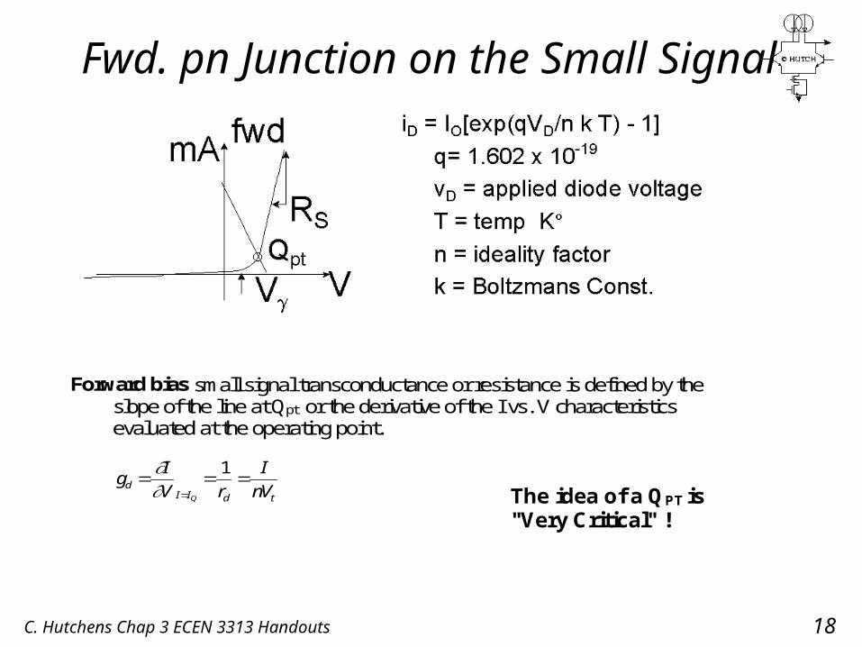
Fwd. pn Junction on the Small Signal
Forward bias small signal transconductance or resistance is defined by theslope of the line at Qpt or the derivative of the I vs. V characteristicsevaluated at the operating point.
gI
V r
I
nVdI I d tQ
1
The idea of a QPT is"Very Critical" !

C. Hutchens Chap 3 ECEN 3313 Handouts 19
Fwd. pn Junction-Diffusion Cap.
CD = T I/Vt = TT I/Vt diffusion cap
EX IF a Diode is forward biased by a ID = 0.1mA current find the small signalac model for a the diode the on voltage (VDQ) across the diode. Assumea Si diode with n=N=1, TT= 27.5nS, CJ0 = 8.3pFd and Is= IS= 2fA
rd = nVt /I = 25mV/0.1mA = 250 ohms
CD = (27.5nS) (0.1mA)/25mV 110pFd
Ctotal = CD + CJ 110pFd + 8.3pFd = 118pFd Note we could just as wellhave ignored CJ
VD = n Vt Ln (ID/IS) = 25mV Ln (0.1mA/2fA) = 0.640V

C. Hutchens Chap 3 ECEN 3313 Handouts 20
Small Signal vs Large Signal
Observations IDQ = (V-VDQ)/R, VDQ = n Vt Ln (IDQ/IS) Transindental functions
require iterations.
Cblock is selected Large enough at time to appear as a short circuitin the frequecy band if intrest.
Vbias DC voltage to set IDQ apperas as a short circuit.
Depending on the value of R vs rd it may be possible to ignored.
Node equation across diode vd
vd (G + gd + sCj + s Cd + (vd - vin ) sCblock= 0
vd/vin = sCblock/(G+ gd + s Ctotal) (Cblock/Ctotal){1/( 1 + gd/sCtotal)}
Typically RS= RS
should beignoreable untilVDQ exceeds 700to 800mV. Thecriteria is rd << RS

C. Hutchens Chap 3 ECEN 3313 Handouts 21
DC vs AC (Small signal)
Observations:
C is selected large enough to appear as a short circuit in the frequency band of theac generator.
To get started quickly V is selected equal 0.6V and should be checked at times withVD = n Vt Ln (ID/IS) = 25mV Ln (4mA/2fA) = 0.710V.
Note that rd can be ignored for all intent and purposes. What is more important is that ID notdestroy the diode or its reverse voltage not be exceeced.
C. Hutchens Chap 3 ECEN 3313 Handouts 22
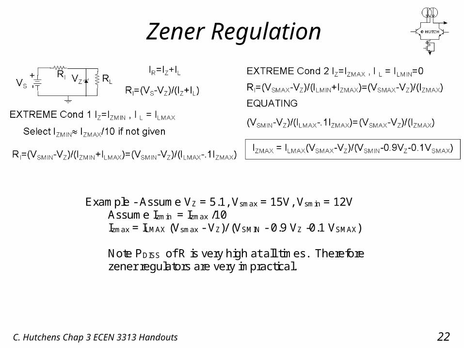
Zener Regulation
Example - Assume VZ = 5.1, Vsmax = 15V, Vsmin = 12VAssume Izmin = Izmax /10Izmax = ILMAX (Vsmax - VZ)/ (VSMIN - 0.9 VZ -0.1 VSMAX)
Note PDISS of R is very high at all times. Thereforezener regulators are very impractical.

C. Hutchens Chap 3 ECEN 3313 Handouts 23
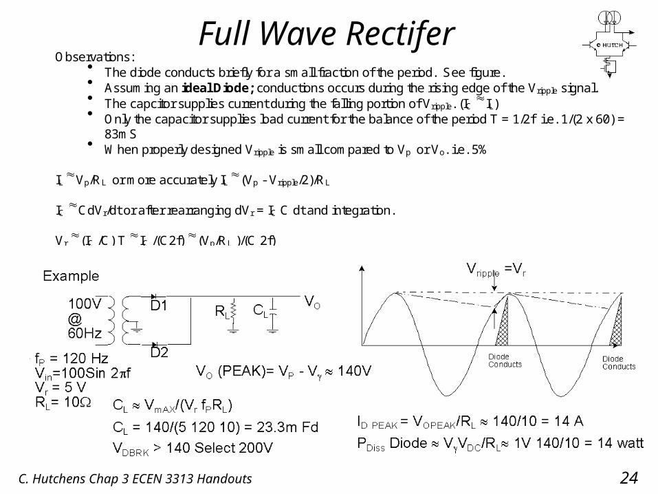
Full Wave Rectifer
Given Ckt diagram andVp = 169 V for 120VrmsVZ = 5V, IZ min = 5mA
Analysis of operationVxpeak = 169/14 12V
@ RL = Ixmax = (Vxpeak -VZ)/R1 = (12-5)/220 = 31.8mA Sets zener powerdissapation. (This should be increased by 10% for saftey purposes)
Vxmin = (IL+ Izmin)R1 + VZ = (5/3.8K + 5mA )220 + 5 = 5.29 V Minimumallowable voltage for zener operation.
Note proper selection of C insures that Vxmin will not be exceeded.
C> Imax dt/dv from I = Cdv/dt where Imax = IL+ Izmin 6.25mAwhere worst case dv/dt = (Vxpeak - Vxmin)2f = (12-5.29)120
C > 6.25mA/{(12-5.29)(120)} 7.8uFd
I = Cdv/dt &
f = /2 = 1/T
C. Hutchens Chap 3 ECEN 3313 Handouts 24
Full Wave RectiferObservations:
The diode conducts briefly for a small fraction of the period. See figure. Assuming an ideal Diode; conductions occurs during the rising edge of the Vripple signal. The capcitor supplies current during the falling portion of Vripple. (IC IL) Only the capacitor supplies load current for the balance of the period T = 1/2f i.e. 1/(2 x 60) =
83mS When properly designed Vripple is small compared to Vp or Vo. i.e. 5%
IL Vp/RL or more accurately IL
(Vp - Vripple/2)/RL
IC CdVr/dt or after rearranging dVr = IC C dt and integration.
Vr (IC /C) T IC /(C2f) (Vp/RL )/(C 2f)

C. Hutchens Chap 3 ECEN 3313 Handouts 25
Voltage Doubler/Clamped Cap
Neg 1/2 cycle D1 conducts
Pos 1/2 cycle D2 conducts
How much loss occures due to the diodes?How do we determine Pdiss require of the diodes?How many additional diodes may be added to increasethe voltage further?
Is ripple on the capacitor a problem and if so can we solveit?

C. Hutchens Chap 3 ECEN 3313 Handouts 26
Diode Switching

C. Hutchens Chap 3 ECEN 3313 Handouts 27
Diode SPICE parameters
.MODEL D1N914/125C D (+ IS = 2.25833E-15 Saturation Current+ RS = 1.799439 Contact Resistance+ N = 1.067043 Ideality factor+ TT = 1.46E-7 Fwd Transit time+ CJO = 3.0177E-12 Zero Bias Junction C+ VJ = 0.4 Built in potential+ M = 0.2147523 doping grading Coeff.+ EG = 1.11+ XTI = 4.799594+ KF = 0+ AF = 1+ FC = 0.764906+ BV = 94 Breakdown Voltage+ IBV = 5E-6+ )
C. Hutchens Chap 3 ECEN 3313 Handouts 28
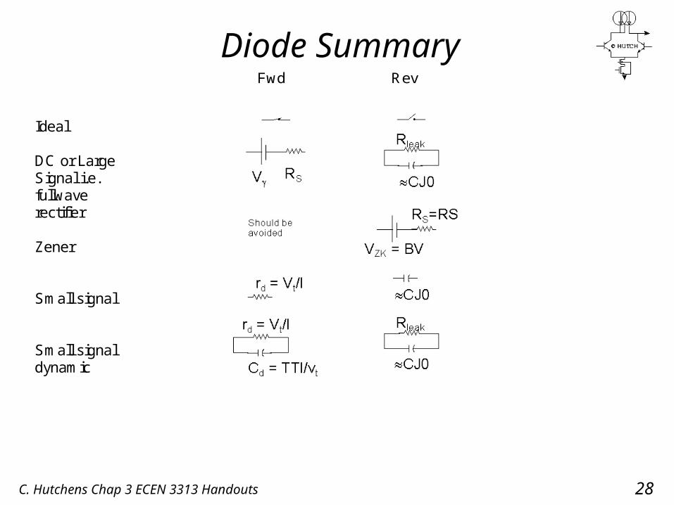
Diode Summary
Ideal
DC or LargeSignal i.e.fullwaverectifier
Zener
Small signal
Small signaldynamic
Fwd Rev


![[Presen]chap 3](https://img.pdfslide.net/doc/110x75/5563be9cd8b42a38198b556e/presenchap-3.jpg)