Embed Size (px)
Citation preview

Chap1. Fundamentals.1
Fundamentals on Testing and Design for Testability

Chap1. Fundamentals.2
Design Verification, Testing and Diagnosis
• Design Verification: Ascertain the design perform its specified behavior
• Testing: Exercise the system and analyze the response to ascertain whether it behaves correctly
• Diagnosis: To locate the cause of misbehavior after the incorrect behavior is detected

Chap1. Fundamentals.3
Some Real Defects in Chips
• Processing Faults– missing contact windows
– parasitic transistors
– oxide breakdown
• Material Defects– bulk defects (cracks, crystal imperfections)
– surface impurities (ion migration)
• Time-Dependent Failures– dielectric breakdown
– electromigration
• Packaging Failures– contact degradation
– seal leaks
Chap1. Fundamentals.4
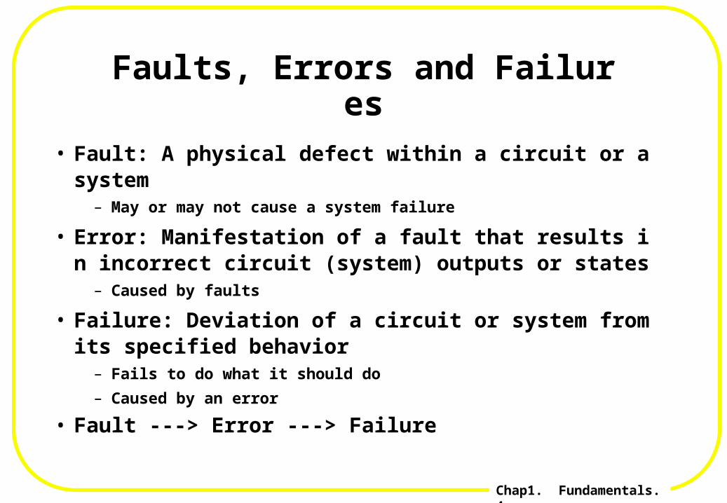
Faults, Errors and Failures
• Fault: A physical defect within a circuit or a system– May or may not cause a system failure
• Error: Manifestation of a fault that results in incorrect circuit (system) outputs or states
– Caused by faults
• Failure: Deviation of a circuit or system from its specified behavior
– Fails to do what it should do
– Caused by an error
• Fault ---> Error ---> Failure

Chap1. Fundamentals.5
Scenario for Manufacture Test
TEST VECTORS
MANUFACTUREDCIRCUIT
COMPARATOR
CIRCUIT RESPONSE
PASS/FAIL
CORRECTRESPONSES

Chap1. Fundamentals.6
Purpose of Manufacture Testing
• Verify Manufacture of Circuit– Improve System Reliability
– Diminish System Cost
• Cost of repair goes up by an order of magnitude each step away from fab line
0.5
5
50
500
ICTest
BoardTest
SystemTest
WarrantyRepair
10
1
100
1000
Costper
fault(Dollars)
B. Davis, The Economics of Automatic Testing , McGRAW-HILL, 1982.
Chap1. Fundamentals.7
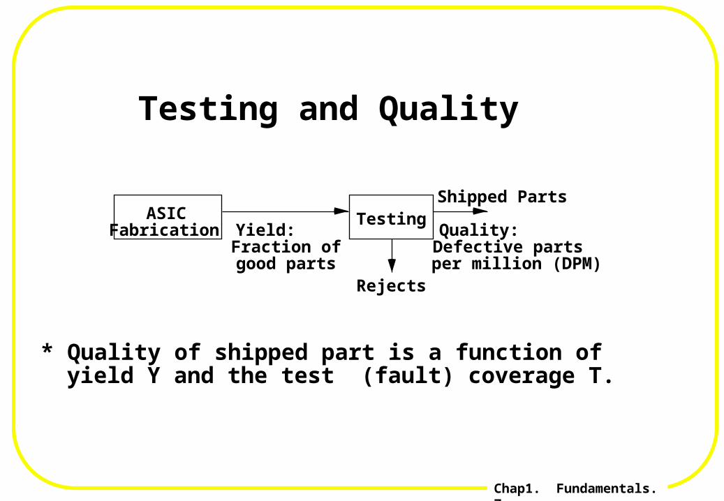
Testing and Quality
ASICFabrication
TestingYield:Fraction ofgood parts
Rejects
Shipped Parts
Quality:Defective partsper million (DPM)
* Quality of shipped part is a function ofyield Y and the test (fault) coverage T.
Chap1. Fundamentals.8
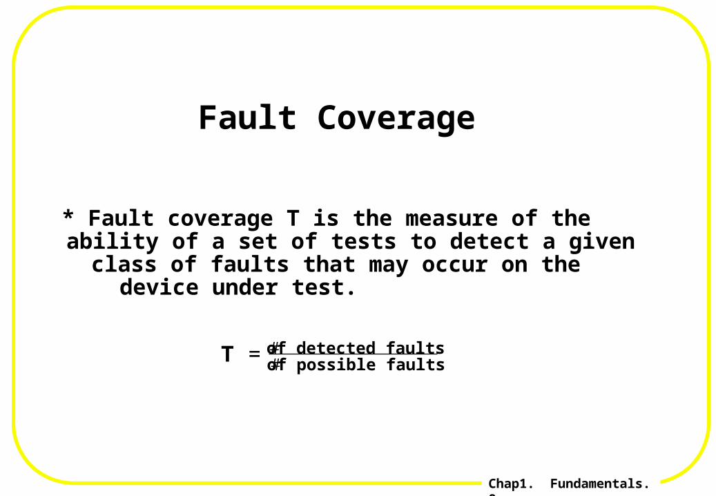
Fault Coverage
* Fault coverage T is the measure of theability of a set of tests to detect a givenclass of faults that may occur on thedevice under test.
T = # of detected faults# of possible faults

Chap1. Fundamentals.9
Defect Level
* Defect Level, DL is the fraction of theshipped parts that are defective.
DL = 1 - Y (1-T )
Y: yield
T: fault coverage

Chap1. Fundamentals.10
Relating Defect Level to Fault Coverage
0 10 20 30 40 50 60 70 80 90 1000
.1
.2
.3
.4
.5
.6
.7
.8
.9
1
Y=.99
Y=.90
Y=.75
Y=.50
Y=.25
Y=.10
Y=.01
Y = Yield
Fault Coverage, T (%)
DL = 1 - Y(1-T)
Chap1. Fundamentals.11
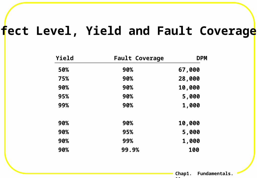
Defect Level, Yield and Fault Coverage
50% 90% 67,000
75% 90% 28,000
90% 90% 10,000
95% 90% 5,000
99% 90% 1,000
90% 90% 10,000
90% 95% 5,000
90% 99% 1,000
90% 99.9% 100
Yield Fault Coverage DPM

Chap1. Fundamentals.12
ASIC
• What is ASIC: Application Specific Integrated Circuits
– Why we need ASICs
• Microelectronic economics– Volume
– Time to market
– Quality

Chap1. Fundamentals.13
ASICs' Demand
* While ASIC density and complexity have
exploded, global market pressures have
increased the demand for both QualityQuality
and Quick TurnaroundQuick Turnaround .

Chap1. Fundamentals.14
Test Development Time vs. Testability
Controllability and observability as a percentage of circuit covered
Measured development timesExtrapolated curve
40
35
30
25
20
15
10
5
0 20 40 60 80 100

Chap1. Fundamentals.15
Time-to-Market Model
Lost revenuedue to delay
Time
Growth Stagnation Decline
Delay in reaching market
* 1/81/8 delay of the product
lifetime reduces 1/31/3 revenue.

Chap1. Fundamentals.16
Why Testing is Difficult ?
• Test application time can be exploded for exhaustive testing of VLSI
– For a combinational circuit with 50 inputs, we need 250 = 1.126x10¹⁵ test patterns. Assume one test per 10-7sec, it takes 1.125x10⁸sec = 3.57yrs. to test such a circuit.
– Test generation of sequential circuits are even more difficult.
» Lack of Controllability and Observability ofFlip-Flops (Latches)
• Functional testing may not be able to detect the physical faults

Chap1. Fundamentals.17
How To Do Test
• Fault Modeling – Identify target faults
– Limit the scope of test generation
– Make analysis possible
• Test Generation– Automatical or Manual
• Fault Simulation– Assess completeness of tests
• Testability Analysis– Analyze a circuit for potential problem on test generation
• Design For Testability– Design a circuit for guaranteed test generation
– Introduce both area overhead and performance degradation

Chap1. Fundamentals.18
The New Challenges for VLSI Testing
• Chip, Board, Module & System for high
– Performance
– Density
– Integration
– Reliability

Chap1. Fundamentals.19
Reference:
• 《 Digital Systems testing and testable design 》ISBN : 0 - 7167 - 8179 - 4 Author : Breuer mELVIN a. etc
• 《 VLSI Testing digital and mixed analogure/digital techinques 》 ISBN : 085296 901 5 Author : Stanley Lhurst

Chap1. Fundamentals.20
DEC Alpha Chip (1994)
* 64-bit RISC
* 200 MHz
* 400 MIPS
* 200 Mflops
* 16.813.9-mm die
* 1.68 million Txs
* 431-pin package
* 3.3-V
* 30W power consumption.

Chap1. Fundamentals.21
Multi-Chip Module (MCM)
* IBM Enterprise System/9000* Type 9121Model 320
* Air-Cooled Processor Technology
* Integration of bipolar chips, CMOS SRAMchips, and ECL & DCS logic circuitry in a TCM(thermal conduction module)
(Ref: IBM J. RES. DEVELOP., May 1991)

Chap1. Fundamentals.22
Wafer Scale Integration (WSI)
* ELSA (European Large SIMD Array),a wafer-scale two-dimensional arrayof single-bit processors
* MUSE (Matrix Update Systolic Experiment),MIT Lincoln Laboratory

Chap1. Fundamentals.23
Traditional Design Flow
• Conduct testing after design
DesignSpec.
DesignToo Large
orToo Slow?
Testability Analysis
TestabilityImprovement?
Done
Designfor
Testability
No
YesNo
Yes

Chap1. Fundamentals.24
The Infamous Design/Test Wall
30 years of experience proves thattest after design does not work!
Functionally correct!We're done!
Oh no!What does
this chip do?!
Design Engineering Test Engineering

Chap1. Fundamentals.25
New Design Mission
• Design circuit to optimally satisfy or trade-off their design constraints in terms of area, performance and testability.
PERFORMANCE AREA
TESTABILITY

Chap1. Fundamentals.26
New VLSI Design Flow
Structure LogicSynthesis
Function/Behavior
DesignSpec.
No
Satisfied?
CircuitSynthesis
Placement/Routing
ATPG
MASK
TESTS
Yes
TestabilityAnalysis
TestableDesignRules
Testplan

Chap1. Fundamentals.27
Why Model Faults ?
• I/O function tests inadequate for manufacturing
– Functionality vs. component & interconnection testing
• Exhaustive testing is Prohibitively expensive

Chap1. Fundamentals.28
Why Model Faults ?
• Fault model identifies target faults– Model faults most likely to occur
• Fault model limits the scope of test generation
– Creat tests only for the modeled faults
• Fault model makes effectiveness measurable by experiments
– Fault coverage can be computed for specific test patterns to reflect its effectiveness
• Fault model makes analysis possible – Associate specific defects with specific test patterns

Chap1. Fundamentals.29
Fault Modeling
Modeling the effects of physical defectson the logic function and timing.
• Physical Defects:– Silicon Defects– Photolithographic Defects– Mask Contamination– Process Variations– Defective Oxide

Chap1. Fundamentals.30
Fault Modeling(cont'd)
• Electrical Effects:– Shorts (Bridging Faults)– Opens– Transistor Stuck-On/Open– Resistive Shorts and Opens– Change in Threshold Voltages
• Logic Effects:– Logic Stuck-At-0/1– Slower Transition (Delay Faults)– AND-Bridging, OR-Bridging
Chap1. Fundamentals.31
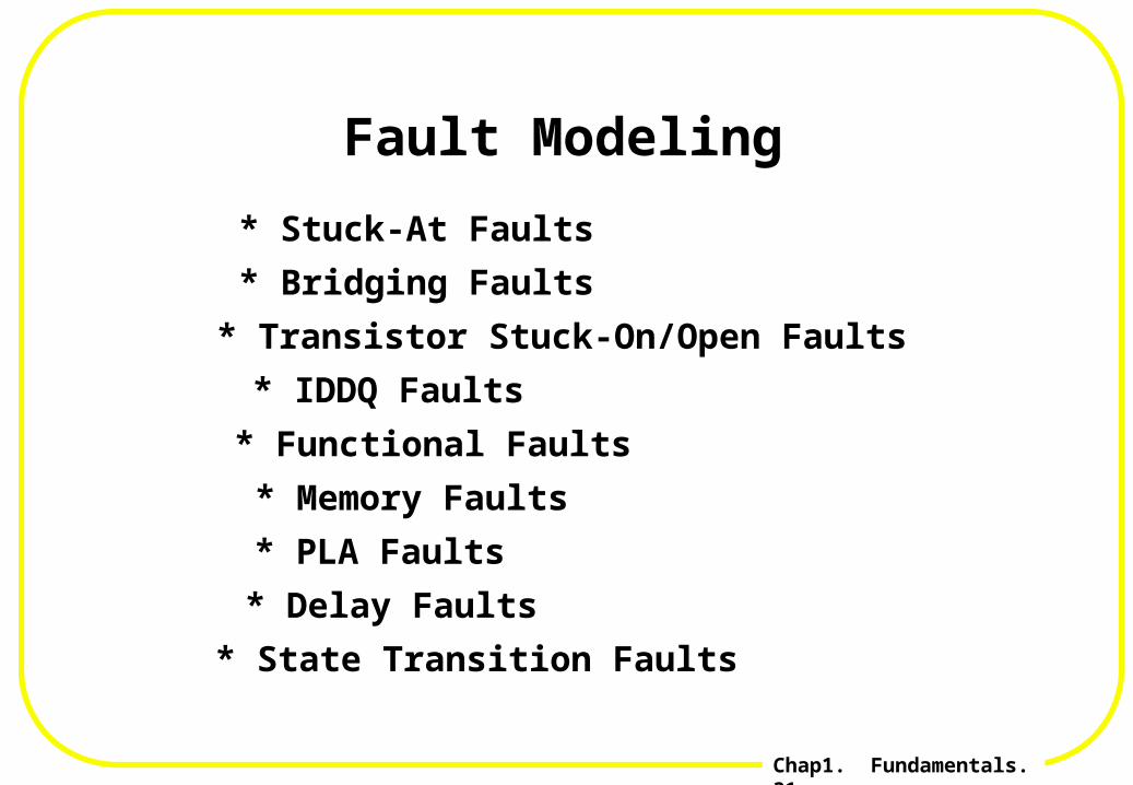
Fault Modeling
* Stuck-At Faults
* Bridging Faults
* Transistor Stuck-On/Open Faults
* IDDQ Faults
* Functional Faults
* Memory Faults
* PLA Faults
* Delay Faults
* State Transition Faults

Chap1. Fundamentals.32
Single Stuck-At Faults
0
1
1
1
0
1/0
1/0
stuck-at-0
True ResponseTest VectorFaulty Response
Assumptions: • Only one line is faulty.• Faulty line permanently set to 0 or 1.• Fault can be at an input or output of a gate.

Chap1. Fundamentals.33
Multiple Stuck-At Faults
• Several stuck-at faults occur at the same time – Important in high density circuits
• For a circuit with k lines– there are 2k single stuck-at faults
– there are 3k-1 multiple stuck-at faults

Chap1. Fundamentals.34
Why Single Stuck-At Fault Model?
* Complexity is greatly reduced.Many different physical defects may be modeled by the same logicalsingle stuck-at fault.
* Single stuck-at fault is technology independent.Can be applied to TTL, ECL, CMOS, etc.
* Single stuck-at fault is design style independent.Gate Arrays, Standard Cell, Custom VLSI
* Even when single stuck-at fault does not accuratelymodel physical defects, the tests derived for logicfaults are still valid for these defects.
* Single stuck-at tests cover a large percentage ofmultiple stuck-at faults.
Chap1. Fundamentals.35
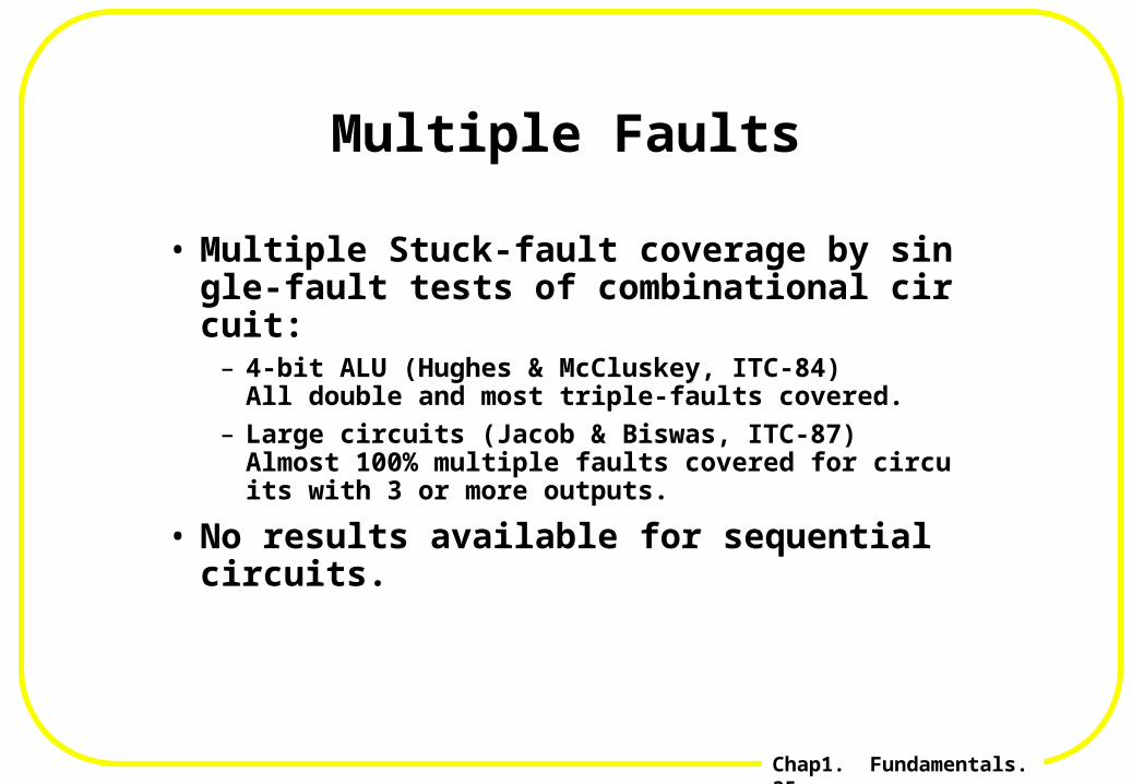
Multiple Faults
• Multiple Stuck-fault coverage by single-fault tests of combinational circuit:
– 4-bit ALU (Hughes & McCluskey, ITC-84)All double and most triple-faults covered.
– Large circuits (Jacob & Biswas, ITC-87)Almost 100% multiple faults covered for circuits with 3 or more outputs.
• No results available for sequential circuits.

Chap1. Fundamentals.36
Bridging Faults
A
B
f
g
A
B
f
g
A
B
f
g
A
B
f
g
• Two or more normally distinct points (lines) are shorted together
– Logic effect depends on technology
– Wired-AND for TTL
– Wired-OR for ECL
– CMOS ?

Chap1. Fundamentals.37
CMOS Transistor Stuck-ON
0 stuck-on
?
IDDQ
* Transistor stuck-on may causeambiguous logic level.
* When input is low, both P and Ntransistors are conducting causingincreased quiescent current, calledIDDQ fault.
–depends on the relative impedances of the pull-up & pull-down networks

Chap1. Fundamentals.38
CMOS Transistor Stuck-OPEN
0
stuck-open
? = previous state
* Transistor stuck-open may causeoutput floating.

Chap1. Fundamentals.39
CMOS Transistor Stuck-OPEN(cont'd)
0 1
stuck-open
1 0/0 0
Initializationvector
memorybehaviour
•Can turn the circuit into a sequential one•Stuck-open faults require two-vector tests

Chap1. Fundamentals.40
Fault Coverage in a CMOS Chip
0
20
40
60
80
100
1000 2000 3000
Test Vectors
stuck and open faults
stuck faults only

Chap1. Fundamentals.41
Summary of Stuck-Open Faults
* First report: Wadsack, Bell Syst. Tech. J., 1978
* Recent results: Woodhall, et al, ITC-87
Experiment with 1-micron CMOS chips:
– 4552 chips passed parametric test– 1255 chips (27.57%) failed tests for stuck-at faults– 44 chips (0.97%) failed tests for stuck-open faults– 4 chips with stuck-open faults passed tests for stuck-at faults
Conclusion– Stuck-at faults are about 29 times more frequent than stuck-open faults– About 91% of chips with stuck-open faults may also have stuck-at faults– Faulty chips escaping tests for stuck-at faults = 0.121%

Chap1. Fundamentals.42
Functional Faults
* Fault effects modeled at a higher levelthan logic for function modules, such as
DecodersMultiplexersAddersCountersRAMsROMs

Chap1. Fundamentals.43
Functional Faults of Decoder
f(Li/Lj): Instead of line Li, Line Lj is selected
f(Li/Li+Lj ): In addition to Li, Lj is selected
f(Li/0): None of the lines are selected
2-bitDecoder
A
BAB
ABABAB

Chap1. Fundamentals.44
Memory Faults
• Parametric Faults– Output Levels
– Power Consumption
– Noise Margin
– Data Retention Time
• Functional Faults– Stuck Faults in Address Register, Data Register,
and Address Decoder
– Cell Stuck Faults
– Adjacent Cell Coupling Faults
– Pattern-Sensitive Faults

Chap1. Fundamentals.45
Memory Faults
• Pattern-sensitive faults: the presence of a faulty signal depends on the signal values of the nearby points
– Most common in DRAMs
• Adjacent cell coupling faults– Pattern sensitivity between a pair of cells
0 0 00 d b0 a 0
a=b=0 => d=0a=b=1 => d=1
Chap1. Fundamentals.46
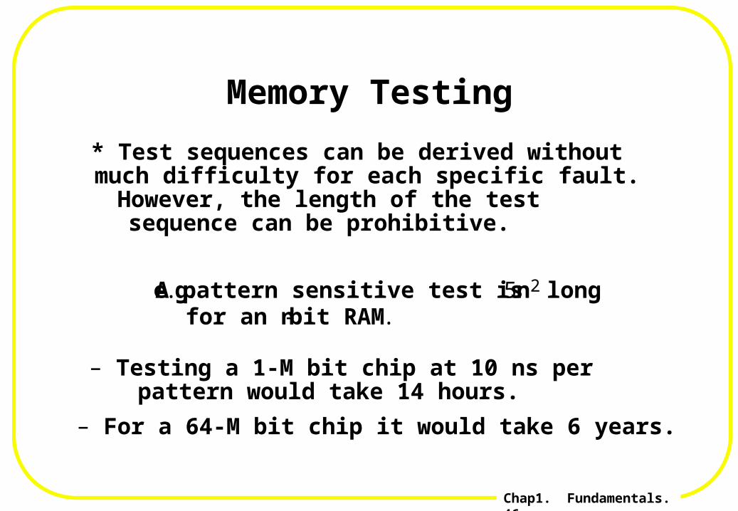
Memory Testing
* Test sequences can be derived withoutmuch difficulty for each specific fault.However, the length of the testsequence can be prohibitive.
e.g. A pattern sensitive test is 5n2 longfor an n -bit RAM .
– Testing a 1-M bit chip at 10 ns perpattern would take 14 hours.
– For a 64-M bit chip it would take 6 years.

Chap1. Fundamentals.47
PLA Faults
* Stuck Faults
* Crosspoint FaultsExtra/Missing Transistors
* Bridging Faults
* Break Faults

Chap1. Fundamentals.48
Stuck Faults in PLA
A B C
f1
f2
P1
P2
A B C f1 f2
P1
P2
AND-Array OR-Array
* S-A-0 & S-A-1 on inputs, inputinvertors, product lines, and outputs
* Easy to simulate in gate model
Gate-level representation

Chap1. Fundamentals.49
Missing Crosspoint Faults in PLA
A B C f1 f2 A B C
f1
f2
Growth
Disappearance
s-a-1
s-a-0
* Missing crosspoint in AND-array-- Growth fault
* Missing crosspoint in OR-array-- Disappearance fault
Equivalent stuck fault representation

Chap1. Fundamentals.50
Extra Crosspoint Faults in PLA* Extra crosspoint in AND-array
-- Shrinkage or disappearance fault
* Extra crosspoint in OR-array-- Appearance fault
Equivalent stuck fault representationA B C f1 f2
A B C
f1
f2
Disapp.
"1"Shrinkage "0"
Appearance

Chap1. Fundamentals.51
Bridging Faults in PLA
* Shorting of adjacent lines (layoutdependent)
* Faulty value identical on shorted lines
* Faulty value AND/OR function ofshorted signals
* A large number of bridging faults mapinto stuck or crosspoint faults
Chap1. Fundamentals.52
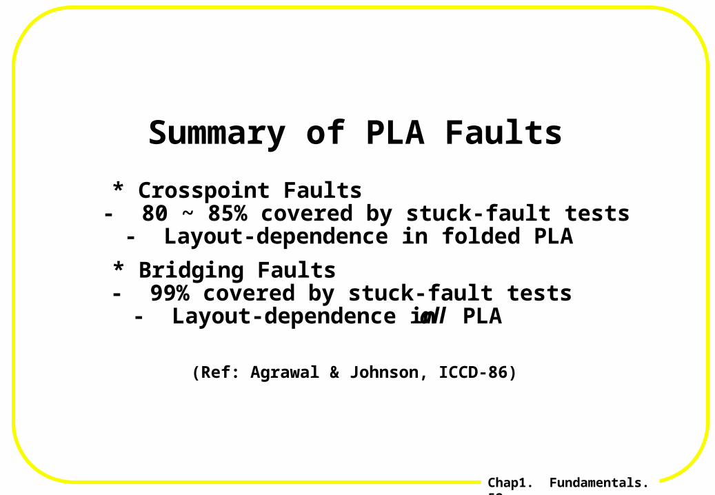
Summary of PLA Faults
* Crosspoint Faults- 80 ~ 85% covered by stuck-fault tests- Layout-dependence in folded PLA
* Bridging Faults- 99% covered by stuck-fault tests- Layout-dependence in all PLA
(Ref: Agrawal & Johnson, ICCD-86)

Chap1. Fundamentals.53
Why Delay Testing?
* There are defects on the chip which allowsit to pass the DC stuck-fault testing, butcauses it to fail when operated at systemspeed.– A chip may pass testing under 1MHz operation but not under 10 MHz

Chap1. Fundamentals.54
Gate-Delay-Fault
• Slow to rise, slow to fall– x is slow to rise when channel resistance R1 is abnormall
y high
VDD VDD
CL
XX
L ---> H
R1
Rp: channel resistance

Chap1. Fundamentals.55
Gate-Delay-Fault
* Disadvantage:
Delay faults resulting from the sumof several small incremental delaydefects may not be detected.
slow

Chap1. Fundamentals.56
Path-Delay-Fault• Propagation delay of the path exceeds
the clock interval.
• The number of paths grows exponentiallywith the number of gates.

Chap1. Fundamentals.57
State Transition Graph
* Each state transition is associated with 4 tuple:(source state, input, output, destination state)
S2 S3
S1
I2/O2 I1/O1

Chap1. Fundamentals.58
Single State Transition Fault Model
S2 S3
S1
I/O I/O
* A fault causes a single state transitionto a wrong destination state.

Chap1. Fundamentals.59
Single State Transition Fault Model
* Has M(N-1) faults for a M-transition N-statemachine
* Is modeled in the state transition level andindependent of implementation
* Is dominated by most physical faults for allpossible implementation
(cont'd)
Chap1. Fundamentals.60
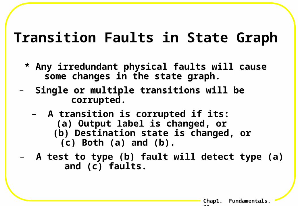
Transition Faults in State Graph
* Any irredundant physical faults will causesome changes in the state graph.
– Single or multiple transitions will be corrupted.
– A transition is corrupted if its:(a) Output label is changed, or(b) Destination state is changed, or(c) Both (a) and (b).
– A test to type (b) fault will detect type (a) and (c) faults.

Chap1. Fundamentals.61
Test for a State Transition Fault
* A test sequence for a fault causing a type (b)corruption on a transition consists of threesubsequences:
(1)Initialization sequence(2) Input label of the faulty transition(3) State-pair differentiating sequence between good and faulty states
CS
S1
S2
S3
Sn
S2'
S3'
Sn'
I1/O1
I/OI'/O'
I1'/O1'
(1)
(2)
(3)

Chap1. Fundamentals.62
Test for a State Transition Fault(cont'd)
* Subsequences (1) and (2) alreadyproduce faulty output responses if theoutput label of the target transition iscorrupted.
* Only need to generate tests for the statetransition faults causing wrongdestination states.

Chap1. Fundamentals.63
Multiple-State-Transition (MST) Faults
* A test sequence that detects allMST faults detects all irredundantphysical fault.
* A machine of M transitions and Nstates has:
NM-1 MST faultsM(N-1) SST faults

Chap1. Fundamentals.64
Why Logical Fault Modeling
• Fault analysis on logic rather than physical problem
– Complexity is reduced
• Technology independent– Same fault model is applicable to many technologies
– Testing and diagnosis methods remain valid despite changes in technology
• Tests derived may be used for physical faults whose effect on circuit behavior is not completely understood or too complex to be analyzed
• Stuck-at fault: The most popular logical fault model

Chap1. Fundamentals.65
Fault Detection
• A test(vector) t detects a fault f iff– t detects f <=>
• Example
x
X1
X2
X3
Z1
Z2
s-a-1
Z1=X1X2 Z2=X2X3
Z1f =X1 Z2f =X2X3
z t z f t 1
The test 100 detects f because z1(100)=0 while z1f (100)=1
z f t z t

Chap1. Fundamentals.66
Sensitization
z (1011)=0 zf (1011)=11011 detects the fault f (G2 stuck-at 1)v/vf : v = signal value in the fault free circuit vf = signal value in the faulty circuit
X1X2
X3
X4
G1
G2
G3
G4
10
1
1
1
s-a-1
0/1
1
0/1
0/1z

Chap1. Fundamentals.67
Sensitization
• A test t that detects a fault f– Activates f (or generate a fault effect) by creating differen
t v and vf values at the site of the fault
– Propagates the error to a primary output w by making all the lines along at least one path between the fault site and w have different v and vf values
• A line whose value in the test changes in the presence of the fault f is said to be sensitized to the fault f by the test
• A path composed of sensitized lines is called a sensitized path

Chap1. Fundamentals.68
Detectability
• A fault f is said to be detectable if there exists a test t that detects f ; otherwise,f is an undetectable fault
• For an undetectable fault f
– No test can simultaneously activate f and create a sensitized path to a primary output
z f x z x

Chap1. Fundamentals.69
Undetectable Fault
• G1 output stuck-at-0 fault is undetectable– Undetectable faults do not change the function of the circui
t
– The related circuit can be deleted to simplify the circuit
x
s-a-0
a
b
c
z
G1

Chap1. Fundamentals.70
Test Set
• Complete detection test set: A set of tests that detect any detectable faults in a class of faults
• The quality of a test set is measured by fault coverage
• Fault coverage: Fraction of faults that are detected by a test set
• The fault coverage can be determined by fault simulation
– >95% is typically required for single stuck-at fault model
– >99.9% in IBM
Chap1. Fundamentals.71
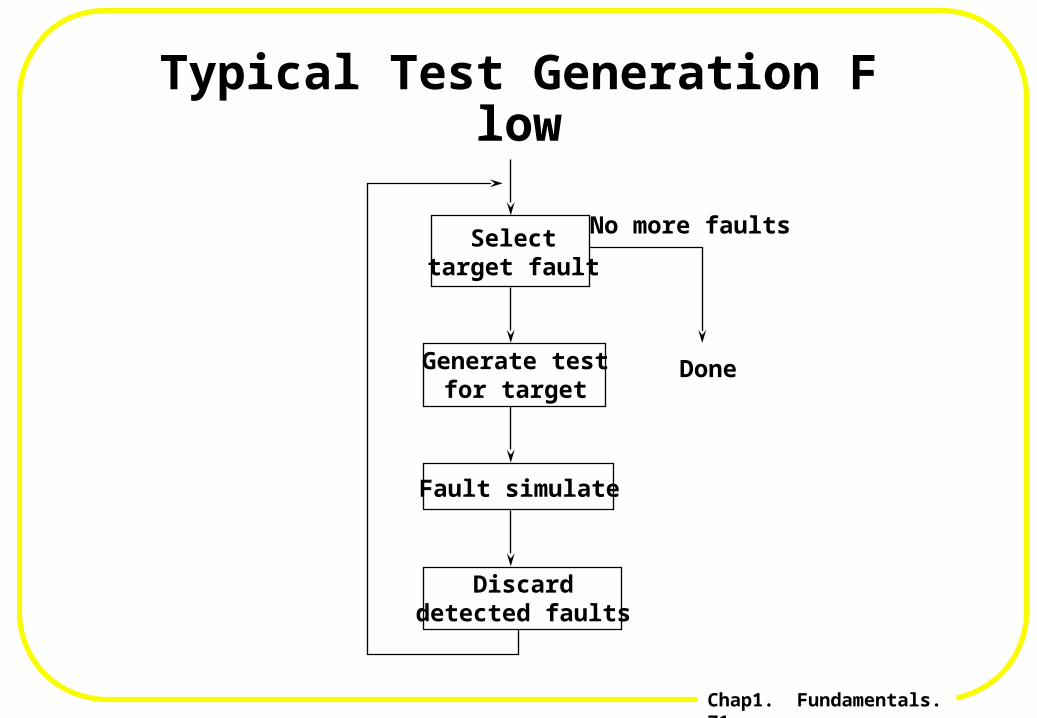
Typical Test Generation Flow
Selecttarget fault
Generate testfor target
Fault simulate
Discarddetected faults
No more faults
Done

Chap1. Fundamentals.72
Fault Equivalence
• A test t distinguishes between faults and if
• Two faults, & are said to be equivalent in a circuit , iff the function under is equal to the function under for any input combination (sequence) of the circuit.
– for all t– No test can distinguish between and – Any test which detects one of them detects all of them
Z t Z t 1
Z t Z t

Chap1. Fundamentals.73
Fault Equivalence
• AND gate: all s-a-0 faults are equivalent
• OR gate: all s-a-1 faults are equivalent
• NAND gate: all the input s-a-0 faults and the output s-a-1 faults are equivalent
• NOR gate: all input s-a-1 faults and the output s-a-0 faults are equivalent
• Inverter: input s-a-1 and output s-a-0 are equivalent input s-a-0 and output s-a-1 are equivalent

Chap1. Fundamentals.74
Equivalence Fault Collapsing
• n+2 instead of 2n+2 faults need to be considered for n-input gates
s-a-1
s-a-1
s-a-1
s-a-1
s-a-1
s-a-1
s-a-1
s-a-1
s-a-0
s-a-0
s-a-0
s-a-0
s-a-0
s-a-0
s-a-0
s-a-0

Chap1. Fundamentals.75
Equivalencein a Wire
* B-sa0 and B-sa1 need not to beconsidered.
A B
* Fault equivalence:
A sao <---> B sao
A sa1 <---> B sa1

Chap1. Fundamentals.76
Fault Equivalence
• Two equivalent faults are detected by exactly the same tests
– three faults shown are equivalent
s-a-1
s-a-0 s-a-1
x
xx

Chap1. Fundamentals.77
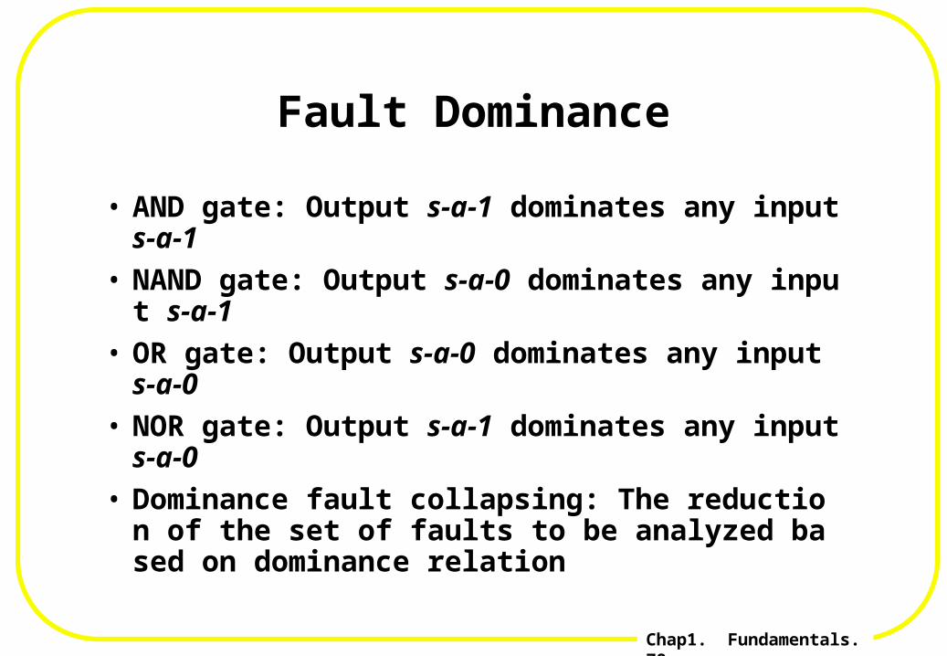
Fault Dominance
• A fault is said to dominate another fault in an irredundant circuit, iff every test (sequence) for is also a test (sequence) for .
– No need to consider fault for fault detection
Chap1. Fundamentals.78
Fault Dominance
• AND gate: Output s-a-1 dominates any input s-a-1
• NAND gate: Output s-a-0 dominates any input s-a-1
• OR gate: Output s-a-0 dominates any input s-a-0
• NOR gate: Output s-a-1 dominates any input s-a-0
• Dominance fault collapsing: The reduction of the set of faults to be analyzed based on dominance relation

Chap1. Fundamentals.79
Fault Dominance
• Detect A sa1:
• Detect C sa1:
C sa1 --> A sa1
• Similarly C sa1 --> B sa1 C sa0 --> A sa0 C sa0 --> B sa0
z t z f t CDCE DCE D CD1
C0, D1
z t z f t CDCE DE 1
C0, D1 or C0, E1
A
B
C
D
Ex
x
x

Chap1. Fundamentals.80
Equivalence & Dominancein a Single-Gate
A
B
C
A B CA
sa1B
sa1C
sa1A
sa0B
sa0C
sa0
0 0 0
0 1 01 0 0
1 1 1
11
1
11
0 0 0
A sa0 <---> B sa0 <---> C sa0
C sa1 ---> A sa1C sa1 ---> B sa1
* Fault equivalence:
* Fault dominance:
* A-sa0 , B-sa0, and C-sa1 need notto be considered.

Chap1. Fundamentals.81
Fault Collapsing
• For each n-input gate, we only need to consider n+1 faults

Chap1. Fundamentals.82
Prime Fault
• is a prime fault if every fault that is dominated by is also equivalent to
• Representative Set of Prime Fault (RSPF)– A set that consists of exactly one prime fault
from each equivalence class of prime faults
– True minimal RSPF is difficult to find
Chap1. Fundamentals.83
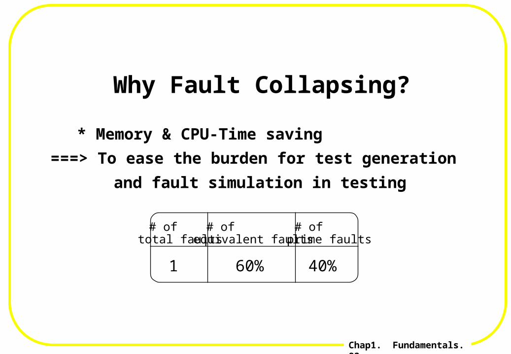
Why Fault Collapsing?
# oftotal faults
# ofequivalent faults
# ofprime faults
1 60% 40%
* Memory & CPU-Time saving
===> To ease the burden for test generation
and fault simulation in testing
Chap1. Fundamentals.84
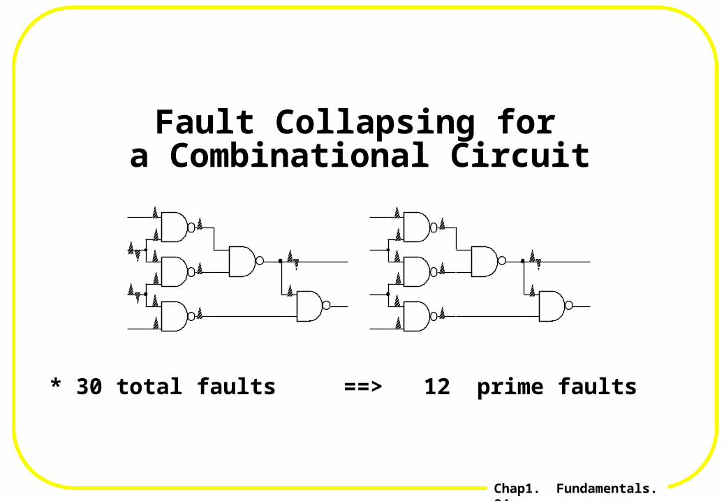
Fault Collapsing fora Combinational Circuit
* 30 total faults ==> 12 prime faults
Chap1. Fundamentals.85
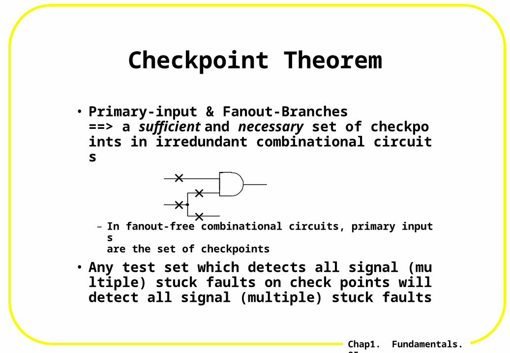
Checkpoint Theorem
• Primary-input & Fanout-Branches==> a sufficient and necessary set of checkpoints in irredundant combinational circuits
– In fanout-free combinational circuits, primary inputs are the set of checkpoints
• Any test set which detects all signal (multiple) stuck faults on check points will detect all signal (multiple) stuck faults

Chap1. Fundamentals.86
Fault Collapsing
• The set of checkpoint faults can be further collapsed by using equivalence and dominance relation
• Example
– 10 checkpoint faults
– a s-a-0 <-> d s-a-0 , c s-a-0 <-> e s-a-0b s-a-0 -> d -> 0 , b s-a-1 -> d -> 1
– 6 tests are enough
a
b
c
d
e
f
g
h

Chap1. Fundamentals.87
Problem
1.1 If the yield of good dice is 90%, and we want a defect level not to exceed 0.1%, what level of testing in terms of fault coverage must be achieved?
1.2 Given the market entry time verse revenue curves as shown in the figure, fill in the following formula
1a. Lost Revenue = Total Expected Revenue * [ ]; The answer should be in term of d and w. d is the delay entry, 2w is the product life. The two market growth rates are the same.
1b. Given a product with total expected revenue $100M, product life is 20 months, What is the revenue loss due to the one month late to the market?
TIME
$ Revenue
Revenue Curve for On Time Market Entry
Revnue Curve for Delayed Markey Entry
Delay = d
Market Window = w
Product Life = 2w

Chap1. Fundamentals.88
1.3 For state transition fault model, explain why there are M(N-1) faults for a M-transition N-state machine.
Similarly explain why there are NM-1 multiple state transition faults.
1.4 For PLA, there are missing crosspoints and extra crosspoints faults in both AND-plane and OR-plane.
Can missing crosspoints be modeled as equivalent stuck-at faults? Why?
Can extra crosspoints be modeled as equivalent stuck-at faults? Why?

Chap1. Fundamentals.89
1.5 For the PLA design shown in Figure 1, construct the Karnaugh maps for Y1,Y2
and Y3 for each of the following situation.
(a) The original PLA;
(b) A shrinkage fault caused by an extra connection between bit line b2 and product line P4;
(c) An appearance fault caused by an extra connection between P3 and Y1;
(d) A growth fault caused by the missing connection between bit line b4 and P3;
(e) A disappearance fault caused by the missing connection between P1 and Y3;
X1 X2 X3
P2=X2X3
P1=X1X2
P3=X2X3P4=X2X3
Y3=P1+P4Y2=P3+P4Y1=P1+P2
b1 b2 b3 b4 b5 b6
AND Plane OR Plane
Figure 1. A PLA example
Chap1. Fundamentals.90
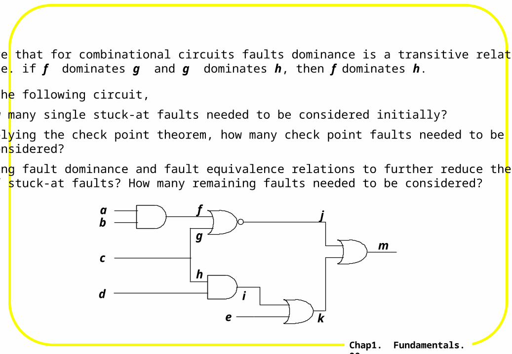
1.6 Prove that for combinational circuits faults dominance is a transitive relation, i.e. if f dominates g and g dominates h, then f dominates h.
1.7 In the following circuit,
a. How many single stuck-at faults needed to be considered initially?
b. Applying the check point theorem, how many check point faults needed to be considered?
c. Using fault dominance and fault equivalence relations to further reduce the number of stuck-at faults? How many remaining faults needed to be considered?
ab
c
d
f
g
h
i
e
j
k
m
Chap1. Fundamentals.91
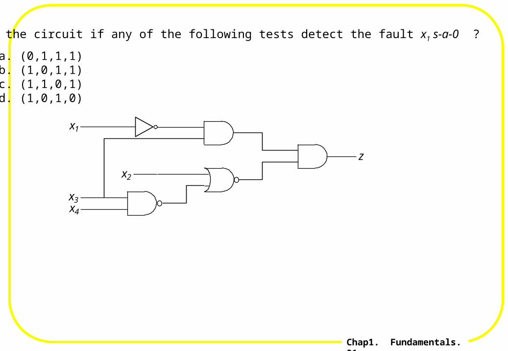
1.8 In the circuit if any of the following tests detect the fault x1 s-a-0 ?
a. (0,1,1,1) b. (1,0,1,1) c. (1,1,0,1) d. (1,0,1,0)
x1
x2
x3x4
z