Embed Size (px)
Citation preview
CHAPTER 1
ANALYSIS AND DESIGN OF BIASING CIRCUITS FOR AMPLIFIERS Dr. K. P. ZachariaIntroduction
The heart of any electronic circuit, whether it is analogue or digital, is an amplifier. An amplifier has three regions of operation, namely, cutoff region, saturation region and a linear region. See, for example, Fig.1.09. The linear region lies between the cutoff and saturation regions. An analogue amplifier is usually constrained or “ biased ’’ to operate in the linear region so that the input signal gets amplified without serious distortion, i.e., the output signal emerges as a reasonably good replica of the input signal. In digital circuits the normal operating regions are the saturation region (level 0) and the cutoff region (level 1). Switching occurs when the operating point shifts from level 0 to level 1, or vice versa, through the linear range. Switching action in a digital circuit can take place only if the circuit behaves like a good amplifier in the linear range. Important performance parameters of a digital circuit, such as switching speed, maximum frequency of switching, etc. are controlled to a large extent, by its behaviour as an amplifier in the linear range. Detailed study of amplifiers is, therefore, essential to understand the operation and limitations of analogue as well as digital circuits.
Amplifiers can be constructed using any of the amplifying devices such as vacuum tubes or solid state devices. Vacuum devices like triodes, tetrodes, pentodes, etc. are currently obsolete. One vacuum device still popular as an amplifier is the traveling wave tube (TWT) used in satellite communication. Solid state devices have lower operating voltages, superior performance, lower power consumption, ease of manufacture, lower cost, etc. compared to vacuum devices. Solid state devices have, therefore, replaced vacuum devices in almost all applications and the process is continuing.
Solid state devices most commonly used for amplification are Bipolar Junction Transistors (BJT’s), Field Effect Transistors (FET’s) and Metal Oxide Semiconductor Field Effect Transistors (MOSFET’s). Since BJT’s are more linear and less expensive, they are preferred in most applications. FET’s and MOSFET’s are used in applications with special requirements such as high input impedance, frequency response extending to several tens of GHz, etc.
- 1 -
SINGLE STAGE AMPLIFIERS
Building a BJT Amplifier
The amplifying behaviour of a BJT can be characterized by the relation
IC = hFE IB + ( 1+hFE ) ICBO ………(1.01)
where, IC is the dc collector current, hFE the dc current gain, IB the dc base current and ICBO the reverse saturation current of the collector junction with emitter terminal open.
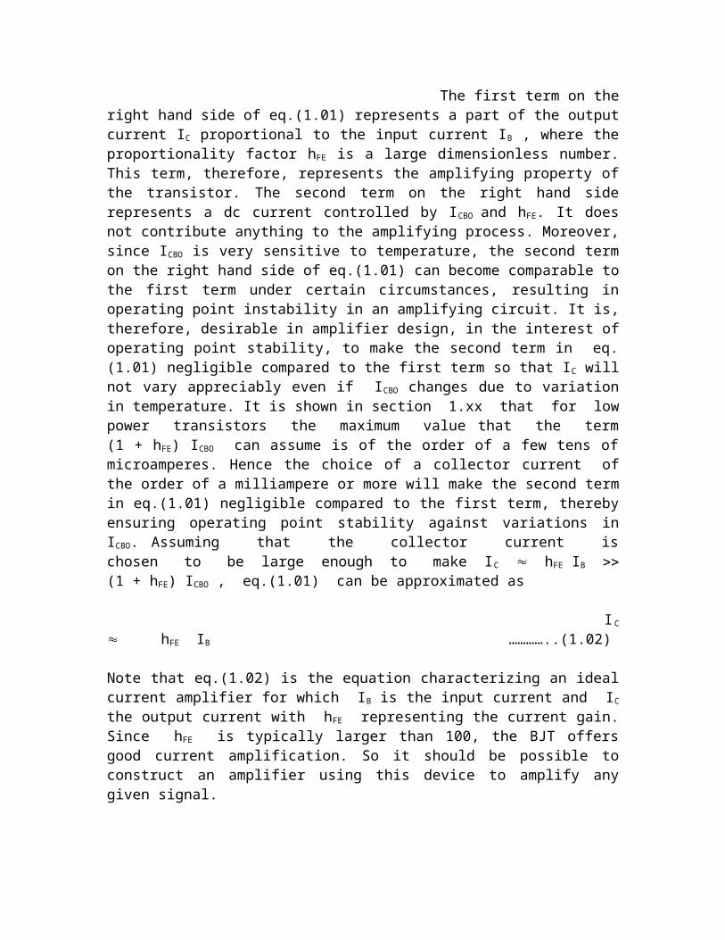
The first term on the right hand side of eq.(1.01) represents a part of the output current IC proportional to the input current IB , where the proportionality factor hFE is a large dimensionless number. This term, therefore, represents the amplifying property of the transistor. The second term on the right hand side represents a dc current controlled by ICBO and hFE. It does not contribute anything to the amplifying process. Moreover, since ICBO is very sensitive to temperature, the second term on the right hand side of eq.(1.01) can become comparable to the first term under certain circumstances, resulting in operating point instability in an amplifying circuit. It is, therefore, desirable in amplifier design, in the interest of operating point stability, to make the second term in eq.(1.01) negligible compared to the first term so that IC will not vary appreciably even if ICBO changes due to variation in temperature. It is shown in section 1.xx that for low power transistors the maximum value that the term (1 + h FE) ICBO can assume is of the order of a few tens of microamperes. Hence the choice of a collector current of the order of a milliampere or more will make the second term in eq.(1.01) negligible compared to the first term, thereby ensuring operating point stability against variations in ICBO. Assuming that the collector current is chosen to be large enough to make IC hFE IB (1 + hFE) ICBO , eq.(1.01) can be approximated as
IC hFE IB …………..(1.02)
Note that eq.(1.02) is the equation characterizing an ideal current amplifier for which IB
is the input current and IC the output current with hFE representing the current gain. Since hFE is typically larger than 100, the BJT offers good current amplification. So it should be possible to construct an amplifier using this device to amplify any given signal.
- 2 -
RS º
Signal Amplifier Load
VS source RL
º
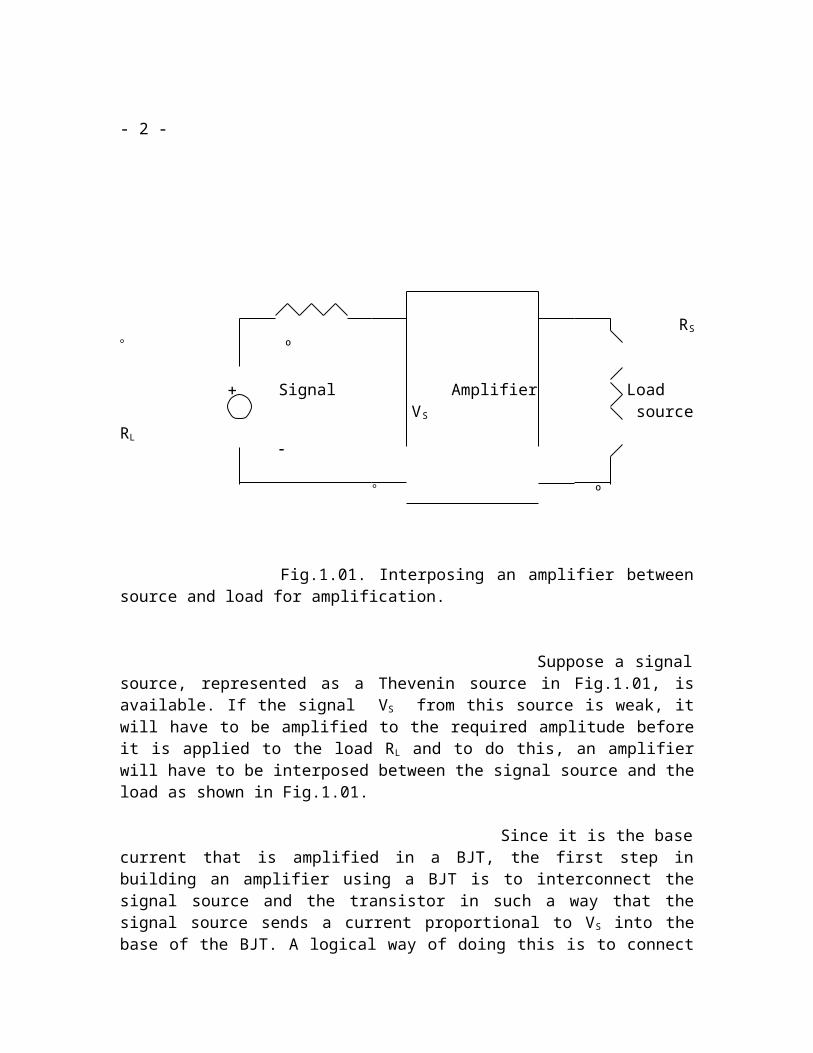
Fig.1.01. Interposing an amplifier between source and load for amplification.
Suppose a signal source, represented as a Thevenin source in Fig.1.01, is available. If the signal VS from this source is weak, it will have to be amplified to the required amplitude before it is applied to the load RL and to do this, an amplifier will have to be interposed between the signal source and the load as shown in Fig.1.01.
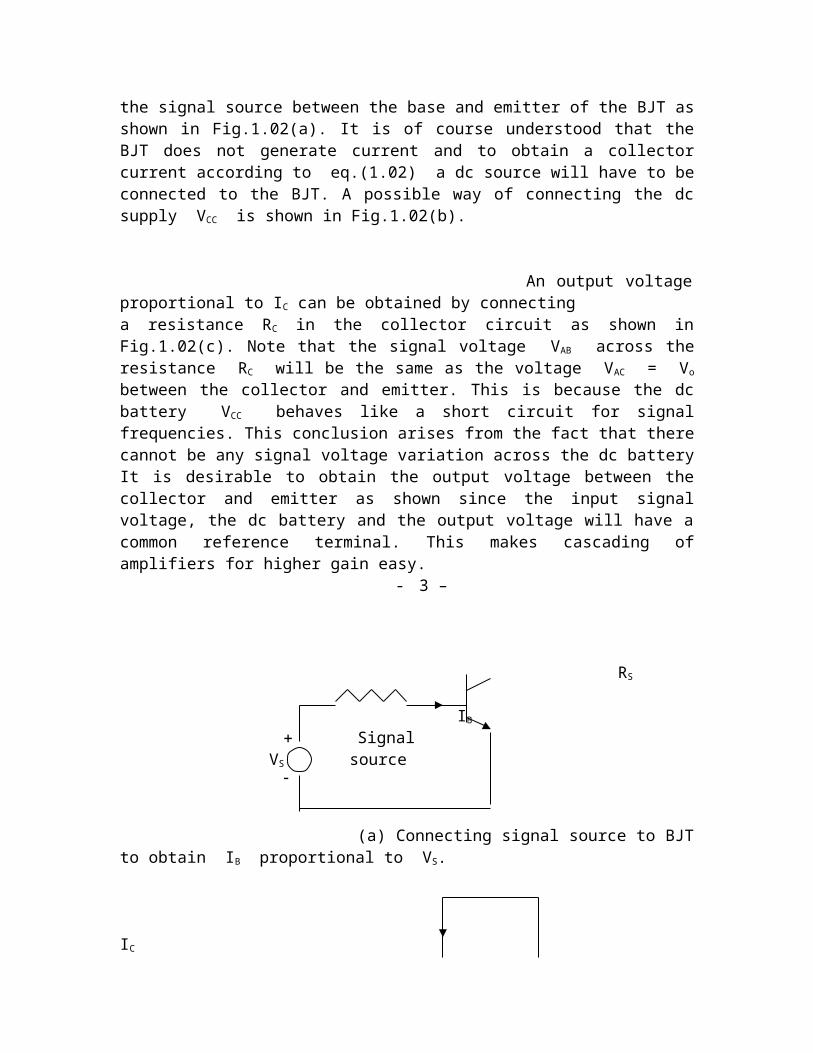
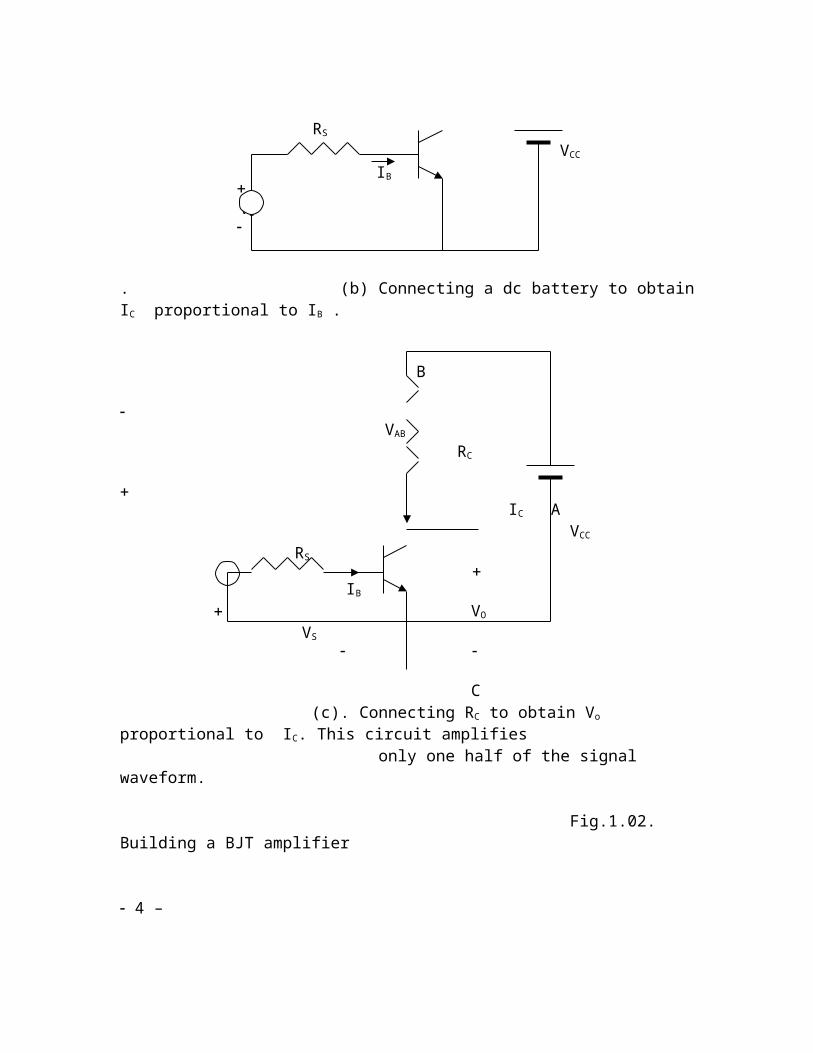
Since it is the base current that is amplified in a BJT, the first step in building an amplifier using a BJT is to interconnect the signal source and the transistor in such a way that the signal source sends a current proportional to VS into the base of the BJT. A logical way of doing this is to connect the signal source between the base and emitter of the BJT as shown in Fig.1.02(a). It is of course understood that the BJT does not generate current and to obtain a collector current according to eq.(1.02) a dc source will have to be connected to the BJT. A possible way of connecting the dc supply VCC is shown in Fig.1.02(b).
An output voltage proportional to IC can be obtained by connecting a resistance RC in the collector circuit as shown in Fig.1.02(c). Note that the signal voltage VAB across the resistance RC will be the same as the voltage VAC = Vo
between the collector and emitter. This is because the dc battery VCC behaves like a short circuit for signal frequencies. This conclusion arises from the fact that there cannot be any signal voltage variation across the dc battery It is desirable to obtain the output voltage between the collector and emitter as shown since the input signal voltage, the dc battery and the output voltage will have a common reference terminal. This makes cascading of amplifiers for higher gain easy.
- 3 –
RS
IB
Signal VS source
(a) Connecting signal source to BJT to obtain IB proportional to VS.
IC
RS
VCC
IB
VS
. (b) Connecting a dc battery to obtain IC proportional to IB .
B VAB
RC
IC A
VCC
RS
IB
VO
VS
C (c). Connecting RC to obtain Vo proportional to IC. This circuit amplifies only one half of the signal waveform.
Fig.1.02. Building a BJT amplifier 4 –
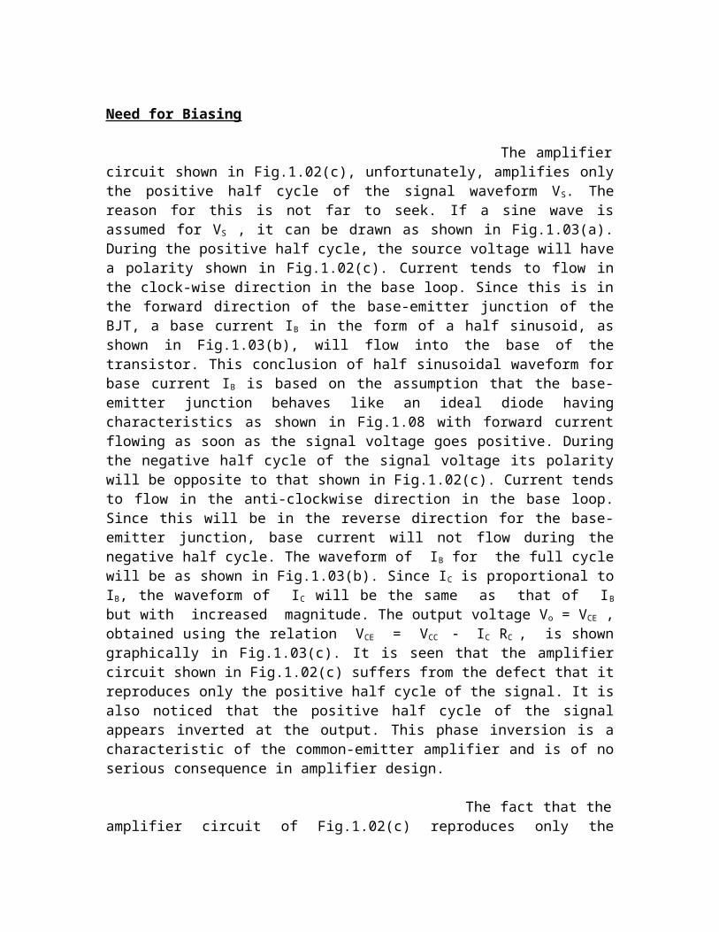
Need for Biasing
The amplifier circuit shown in Fig.1.02(c), unfortunately, amplifies only the positive half cycle of the signal waveform VS. The reason for this is not far to seek. If a sine wave is assumed for VS , it can be drawn as shown in Fig.1.03(a). During the positive half cycle, the source voltage will have a polarity shown in Fig.1.02(c). Current tends to flow in the clock-wise direction in the base loop. Since this is in the forward direction of the base-emitter junction of the BJT, a base current I B in the form of a half sinusoid, as shown in Fig.1.03(b), will flow into the base of the transistor. This conclusion of half sinusoidal waveform for base current IB is based on the assumption that the base-emitter junction behaves like an ideal diode having characteristics as shown in Fig.1.08 with forward current flowing as soon as the signal voltage goes positive. During the negative half cycle of the signal voltage its polarity will be opposite to that shown in Fig.1.02(c). Current tends to flow in the anti-clockwise direction in the base loop. Since this will be in the reverse direction for the base-emitter junction, base current will not flow during the negative half cycle. The waveform of IB
for the full cycle will be as shown in Fig.1.03(b). Since IC is proportional to IB, the waveform of IC will be the same as that of IB but with increased magnitude. The output voltage Vo = VCE , obtained using the relation VCE = VCC IC RC , is shown graphically in Fig.1.03(c). It is seen that the amplifier circuit shown in Fig.1.02(c) suffers from the defect that it reproduces only the positive half cycle of the signal. It is also noticed that the positive half cycle of the signal appears inverted at the output. This phase inversion is a characteristic of the common-emitter amplifier and is of no serious consequence in amplifier design.
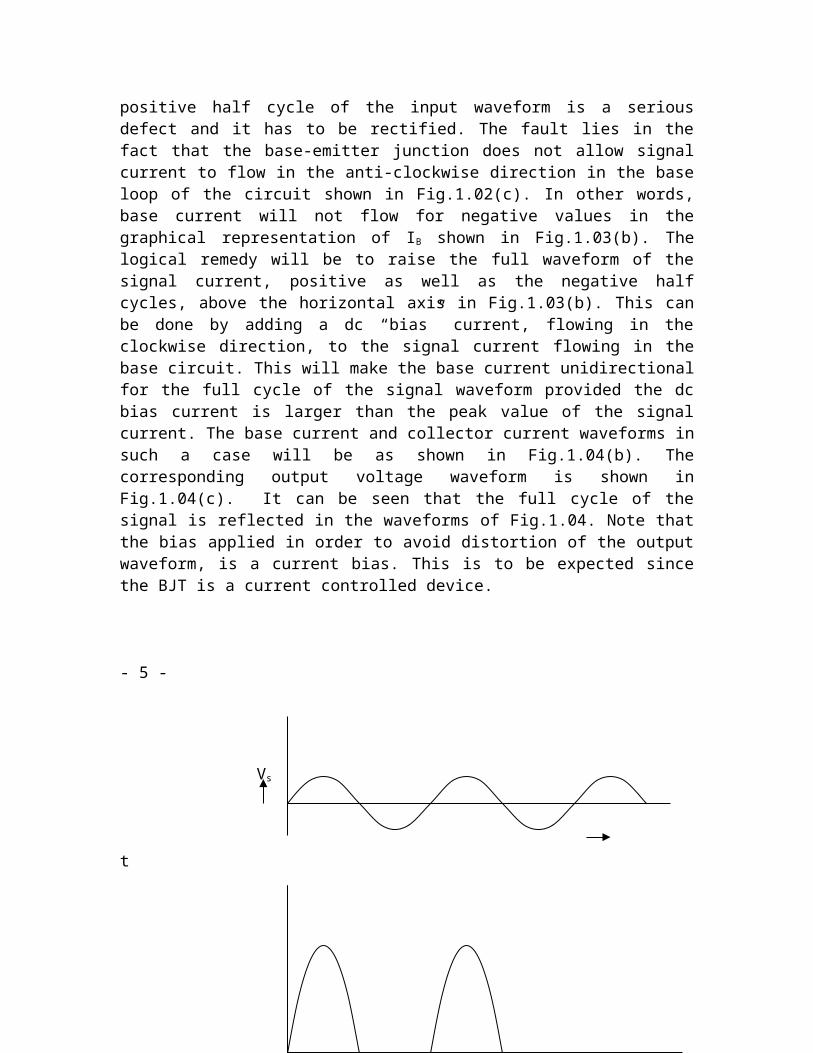
The fact that the amplifier circuit of Fig.1.02(c) reproduces only the positive half cycle of the input waveform is a serious defect and it has to be rectified. The fault lies in the fact that the base-emitter junction does not allow signal current to flow in the anti-clockwise direction in the base loop of the circuit shown in Fig.1.02(c). In other words, base current will not flow for negative values in the graphical representation of IB shown in Fig.1.03(b). The logical remedy will be to raise the full waveform of the signal current, positive as well as the negative half cycles, above the horizontal axis in Fig.1.03(b). This can be done by adding a dc “bias” current, flowing in the clockwise direction, to the signal current flowing in the base circuit. This will make the base current unidirectional for the full cycle of the signal waveform provided the dc bias current is larger than the peak value of the signal current. The base current and collector current waveforms in such a case will be as shown in Fig.1.04(b). The corresponding output voltage waveform is shown in Fig.1.04(c). It can be seen that the full cycle of the signal is reflected in the waveforms of Fig.1.04. Note that the bias applied in order to avoid distortion of the output waveform, is a current bias. This is to be expected since the BJT is a current controlled device. - 5 -
Vs
t
(a) Signal voltage waveform
IB , IC
t
(b) Base and collector current waveforms
VCC
VCE
t
(c) Output voltage waveform
Fig.1.03. Waveforms for the circuit of Fig.1.02(c).
- 6 -
VS
t
(a) Signal voltage waveform
IBdc, ICdc
IB, IC
t(b) Base and collector current waveforms.
VCC
VCEO
VCE
t (c) Output voltage waveform.
Fig.1.04. Waveforms with bias current applied. 7
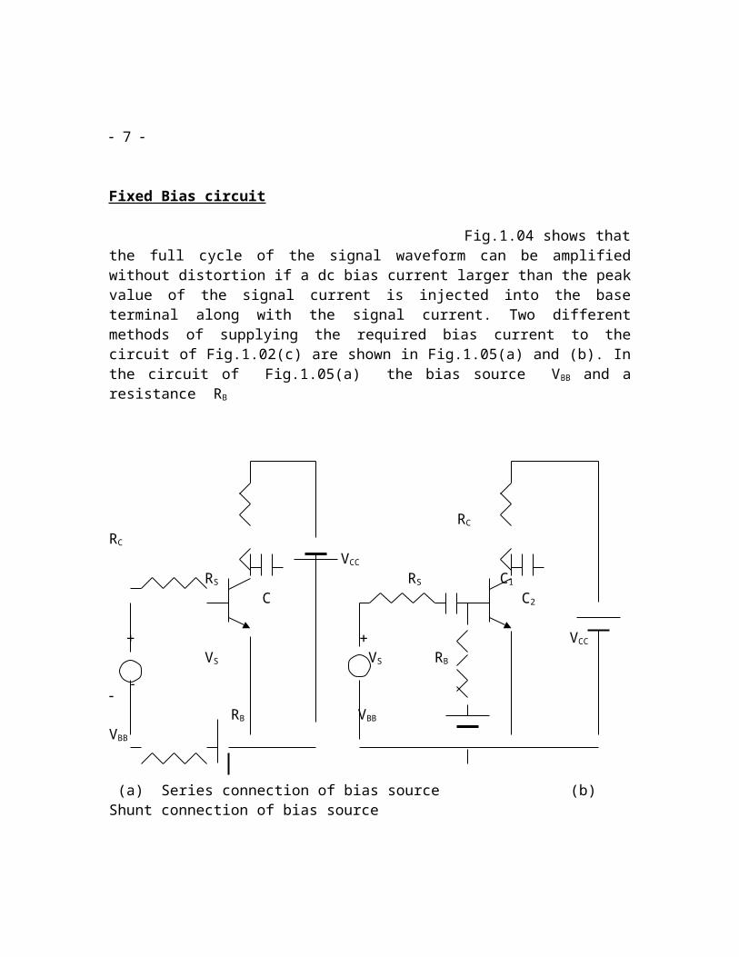
Fixed Bias circuit
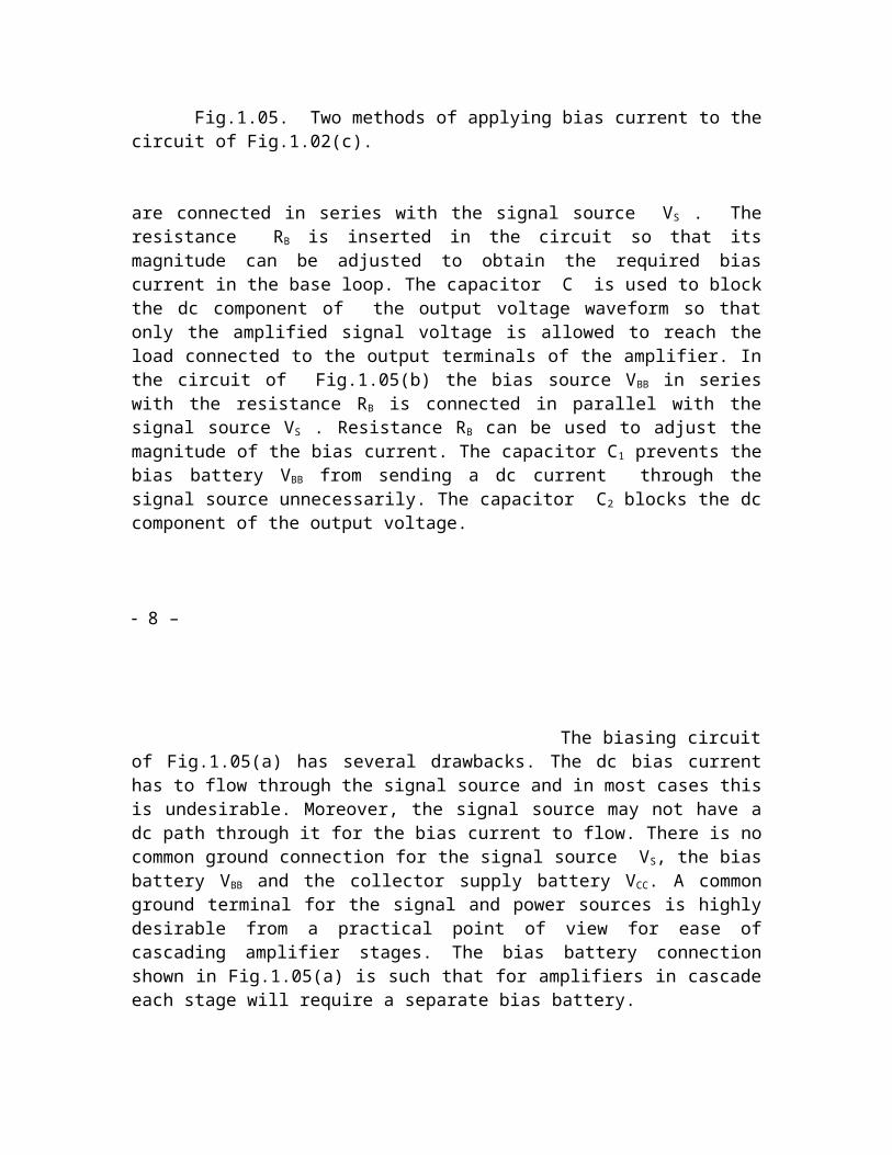
Fig.1.04 shows that the full cycle of the signal waveform can be amplified without distortion if a dc bias current larger than the peak value of the signal current is injected into the base terminal along with the signal current. Two different methods of supplying the required bias current to the circuit of Fig.1.02(c) are shown in Fig.1.05(a) and (b). In the circuit of Fig.1.05(a) the bias source VBB and a resistance RB
RC RC
VCC
RS RS C1 C C2
VCC
VS VS RB
RB VBB VBB
(a) Series connection of bias source (b) Shunt connection of bias source
Fig.1.05. Two methods of applying bias current to the circuit of Fig.1.02(c).
are connected in series with the signal source VS . The resistance RB is inserted in the circuit so that its magnitude can be adjusted to obtain the required bias current in the base loop. The capacitor C is used to block the dc component of the output voltage waveform so that only the amplified signal voltage is allowed to reach the load connected to the output terminals of the amplifier. In the circuit of Fig.1.05(b) the bias source VBB
in series with the resistance RB is connected in parallel with the signal source VS . Resistance RB can be used to adjust the magnitude of the bias current. The capacitor C1
prevents the bias battery VBB from sending a dc current through the signal source unnecessarily. The capacitor C2 blocks the dc component of the output voltage.
8 –
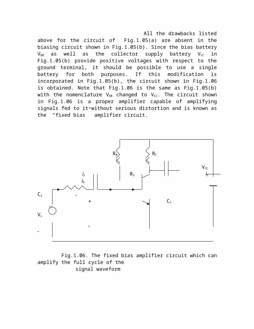
The biasing circuit of Fig.1.05(a) has several drawbacks. The dc bias current has to flow through the signal source and in most cases this is undesirable. Moreover, the signal source may not have a dc path through it for the bias current to flow. There is no common ground connection for the signal source VS, the bias battery VBB and the collector supply battery VCC. A common ground terminal for the signal and power sources is highly desirable from a practical point of view for ease of cascading amplifier stages. The bias battery connection shown in Fig.1.05(a) is such that for amplifiers in cascade each stage will require a separate bias battery.
All the drawbacks listed above for the circuit of Fig.1.05(a) are absent in the biasing circuit shown in Fig.1.05(b). Since the bias battery VBB as well as the collector supply battery VCC in Fig.1.05(b) provide positive voltages with respect to the ground terminal, it should be possible to use a single battery for both purposes. If this modification is incorporated in Fig.1.05(b), the circuit shown in Fig.1.06 is obtained. Note that Fig.1.06 is the same as Fig.1.05(b) with the nomenclature VBB changed to VCC.

The circuit shown in Fig.1.06 is a proper amplifier capable of amplifying signals fed to it without serious distortion and is known as the “fixed bias” amplifier circuit.
RB RC
VCC
is RS is ib
C2
C1 VS Vo
Fig.1.06. The fixed bias amplifier circuit which can amplify the full cycle of the signal waveform
9
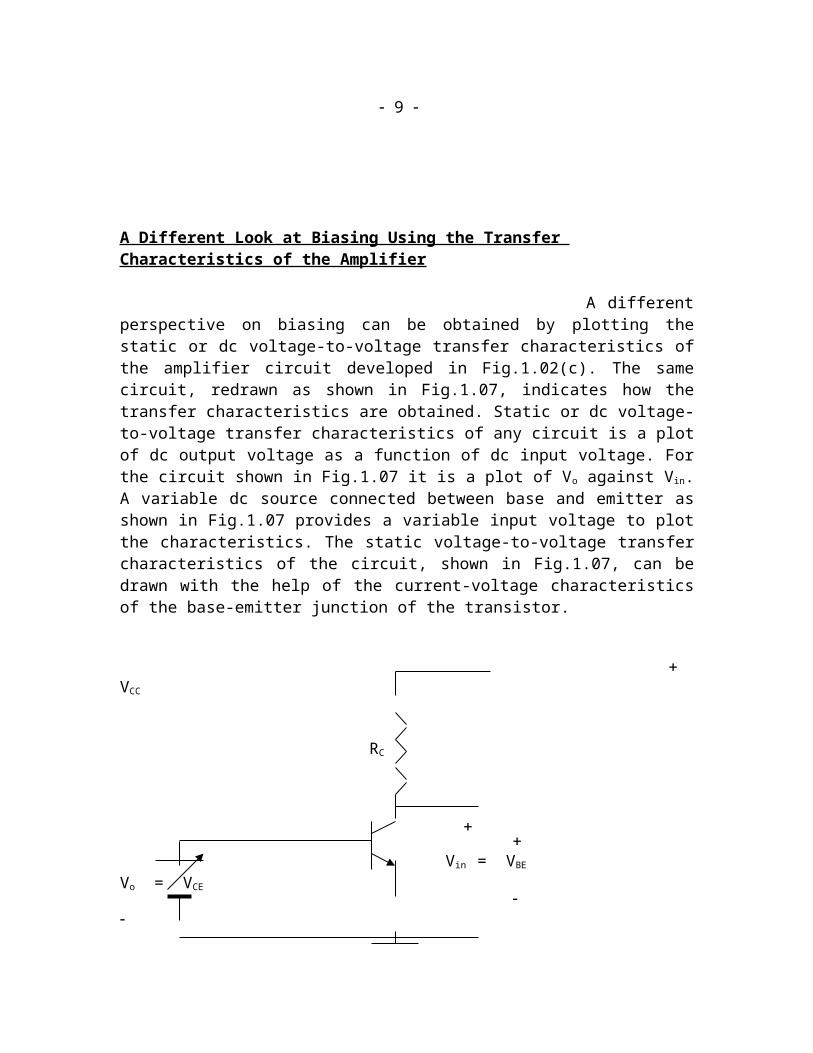
A Different Look at Biasing Using the Transfer Characteristics of the Amplifier
A different perspective on biasing can be obtained by plotting the static or dc voltage-to-voltage transfer characteristics of the amplifier circuit developed in Fig.1.02(c). The same circuit, redrawn as shown in Fig.1.07, indicates how the transfer characteristics are obtained. Static or dc voltage-to-voltage transfer characteristics of any circuit is a plot of dc output voltage as a function of dc input voltage. For the circuit shown in Fig.1.07 it is a plot of Vo against Vin. A variable dc source connected between base and emitter as shown in Fig.1.07 provides a variable input voltage to plot the characteristics. The static voltage-to-voltage transfer characteristics of the circuit, shown in Fig.1.07, can be drawn with the help of the current-voltage characteristics of the base-emitter junction of the transistor.
VCC
RC
Vin = VBE Vo = VCE
- Fig.1.07. Circuit for drawing voltage-to-voltage transfer characteristics
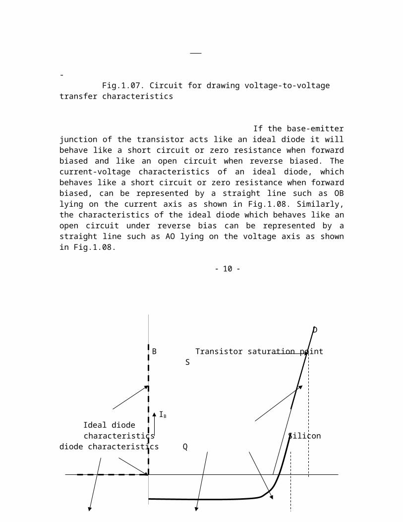
If the base-emitter junction of the transistor acts like an ideal diode it will behave like a short circuit or zero resistance when forward biased and like an open circuit when reverse biased. The current-voltage characteristics of an ideal diode, which behaves like a short circuit or zero resistance when forward biased, can be represented by a straight line such as OB lying on the current axis as shown in Fig.1.08. Similarly, the characteristics of the ideal diode which behaves like an open circuit under reverse bias can be represented by a straight line such as AO lying on the voltage axis as shown in Fig.1.08.
10
D
B Transistor saturation point S
IB
Ideal diodecharacteristics Silicon diode characteristics Q
C E
A O VBE VBEon VBE VBEsat
0.5v 0.6v 0.7v
Fig.1.08. Characteristics of an ideal and an actual silicon base-emitter junction
The current-voltage characteristics of the base-emitter junction of a silicon transistor is represented graphically by the curve AOCD in Fig.1.08. The reverse bias characteristics of both ideal and an actual silicon base-emitter junction can be represented by the same straight line AO since both behave like open circuits under reverse bias. The forward characteristics of the base-emitter junction of an actual transistor, shown by the curve OCD in Fig.1.08, differ significantly from the forward characteristics of the ideal diode represented by the straight line OB in the same figure. The ideal diode allows current to pass freely even with the smallest amount of forward bias. A typical silicon diode, on the other hand, allows significant amount of current to pass through only when the forward bias exceeds approximately 0.5 volts as shown by the curve OCD in Fig.1.08. For this reason VBEon, which is the base emitter voltage at which a silicon transistor begins to conduct noticeably, is assumed to be about 0.5 volts. To simplify the discussion it is assumed that the forward as well as reverse characteristics of the base-emitter junction of a silicon transistor, represented by the curve AOCSD, can be approximated by two straight lines AE and ED without significant error.
11
If the straight line approximation consisting of the straight lines AOE and ED is assumed for the base-emitter junction characteristics of the transistor, it is seen that no base current IB and, correspondingly, no collector current IC will flow through the transistor for all values of reverse bias voltages and for forward bias voltages less than 0.5 volts. So throughout this range, where VBE = Vin , the collector current IC
being zero in the circuit of Fig.1.07, Vo = VCE = VCC IC RC = VCC. This is represented graphically as AOE, the cut off region of the transistor, in the linearised voltage-to-voltage transfer characteristics shown in Fig.1.09.
Cut off point Linear region or VCC Active region A O E
Cut off region Saturation region
dVo
Small-signal gain Av = dVin
Q ( Desirable location foroperating point )
Vo = VCE
Saturation point S D VCEsat = 0.2v
VBEon VBE VBEsat Vin = VBE 0.5v 0.6v 0.7v
Fig.1.09. Linearised voltage-to-voltage transfer characteristics of the circuit of Fig.1.07. When the base-emitter junction of the transistor is forward biased beyond 0.5v base current IB begins to flow, collector current IC becomes noticeable and the output voltage Vo = VCE = VCC IC RC begins to fall. This process continues as forward bias increases beyond 0.5v. This fall of VCE with increasing VBE is represented by the line ES in Fig.1.09. This region, where IC is proportional to IB is known as the active region of the transistor and is shown as such in Fig.1.09. Small-signal gain Av in this region will be equal to dVo dVin .
12
At point S the transistor goes into saturation ( see section 1.xx ). Beyond this point the collector current IC saturates and does not increase even if VBE and, correspondingly, IB is increased. In this region known as the “saturation region” , shown as SD in Fig.1.09, VCE remains constant at around 0.2v . Note that points A,O,E,Q,S and D in Figs.1.09 and 1.10 corresponds to points A,O,E,Q,S and D respectively in Fig.1.08.
Voutac A O C Outputsignal No output No output No output E
VCC Voutac
Vo Q
Voutac
S D
No output
0.2v
Vin A O C E Q S D
Input signal
0.2v 0v 0,2v 0.5v 0.6v 0.7v 1.0v
Fig.1.10. Output waveforms for the circuit of Fig 2.01 for various input waveforms
The process of amplification of ac signals using the unbiased circuit of Fig.1.07 and the problems connected with it can be understood with the help of its voltage-to-voltage transfer characteristics shown in Fig.1.10 along with various input and output ac signal waveforms. If a signal as shown at O ( below the axis ) is applied to
13
the input of the circuit, there will be no output since for this range of input voltage the output voltage remains constant at VCC. This is shown as Voutac at O in the figure. An input waveform, such as that shown at A is obtained by superimposing the signal voltage on a dc bias voltage equal to 0.2 volts. For this waveform as well as the waveform shown at C the output remains zero for all time since the output voltage does not vary within this range of input voltage. For the input waveform shown at E the output voltage does not vary for all negative values of the ac signal. Positive values of the input signal causes the output voltage to drop giving rise to the output wave form shown at E. Note that only the positive half cycles of the input waveform is amplified. The half-waveform is also inverted at the output. The input voltage waveform shown at Q keeps the full waveform in the linear range and, correspondingly, the full waveform appears at the output with reasonable amplification. Such operation makes it a good amplifier and the 0.6 volts dc on which the input signal is superimposed is known as the bias voltage. In well designed linear amplifiers the dc or quiescent bias voltage will be around 0.6v. The case of the input voltage shown at F is similar to that of E, except that in this case only the negative half cycles of the ac signal waveform are amplified with phase inversion. For the input signal waveform shown at D there will be no output since the transistor remains in saturation at VCEsat = 0.2v throughout the full period of the ac signal.
It is seen that the circuit of Fig.1.07 operates as a linear amplifier only if the operation is confined to the linear range of its voltage-to-voltage transfer characteristics for the full cycle of the input signal. It is also seen that the portion of the signal waveform lying outside the linear range is not amplified at all and will produce zero output. Therefore, if maximum peak-to-peak undistorted output is required from the
circuit, it should be biased to operate at the center of its linear range. Note that biasing is used to ensure that the full cycle of the signal waveform is reproduced. Fig.1.08 shows that for a silicon transistor in the active region, i.e., for VBE 0.6v, base current IB varies rapidly for small changes in VBE. Therefore, in amplifier circuits, better control of bias point is obtained if a current bias, which will automatically control the bias voltage, is used. Such a dc bias current IBO for biasing the transistor, can be obtained by connecting a resistor from the base terminal of the transistor to VCC . Connection of this bias resistor to the circuit of Fig.1.07 converts it into the fixed bias amplifier circuit shown in Fig.1.06.
Operating CMOS logic gate as a linear amplifier
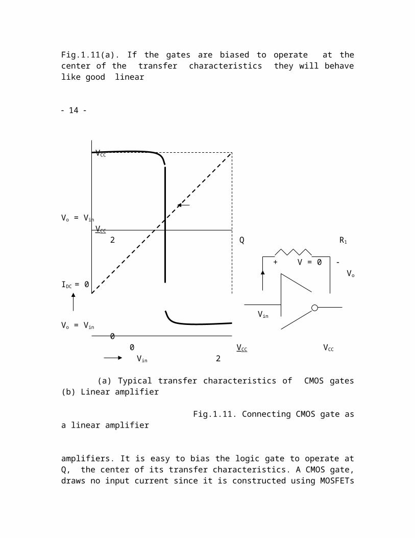
Logic gates, TTL as well as CMOS, has a logic level “one” at a high voltage and a logic level “zero” at a voltage level close to zero. During switching the voltage varies from one level to the other through a linear region. The foregoing discussion suggests that if logic gates are biased to operate in the linear range of their transfer characteristics they will behave like linear amplifiers. The general shape of the transfer characteristics of CMOS gates is as shown in Fig.1.11(a). If the gates are biased to operate at the center of the transfer characteristics they will behave like good linear 14
VCC
Vo = Vin
VCC
2 Q R1
+ V = 0 Vo IDC = 0
Vin Vo = Vin
0 0 VCC VCC
Vin 2 (a) Typical transfer characteristics of CMOS gates (b) Linear amplifier
Fig.1.11. Connecting CMOS gate as a linear amplifier
amplifiers. It is easy to bias the logic gate to operate at Q, the center of its transfer characteristics. A CMOS gate, draws no input current since it is constructed using MOSFETs which have their input gate terminal insulated from the rest of the device by an oxide layer. Therefore, if a resistance R1 is connected between the input and output terminals of the logic gate, as shown in Fig.1.11(b), no dc current will flow through R1
and there will be no voltage across it. This forces the voltage Vo to be equal to Vin. This constraint Vo = Vin is shown graphically as the dotted straight line in Fig.1.11(a). Since the quiescent or dc operating point must obey this constraint it must lie on this line. The quiescent point must also necessarily lie on the transfer characteristics. It follows that the quiescent point lies at Q, the intersection of the dotted line and the transfer characteristics as shown in Fig.2.05(a). Therefore, a resistance connected between the input and output of a CMOS gate forces the quiescent point Q to lie at the center of the transfer characteristics, as required, and makes Vo = Vin = Vcc / 2 . Note that the magnitude of resistance of R1 is immaterial as far as biasing is concerned since no current flows through it. However, the input resistance of the amplifier being dependent on it, low values are avoided. Typical values for R1 rage between 100K and 20M. A similar method is used to bias TTL logic gates to operate them in the linear range.
15
Analysis of amplifier circuits
Introduction
The purpose of analysis, in the present context, is to determine all the dc and ac voltages and currents pertaining to a given amplifier circuit to assess its behaviour as an amplifier. An amplifier can amplify properly only if the operation is restricted to its linear range. DC analysis of the circuit will verify whether the quiescent point lies within the linear range or whether it lies in the cutoff or saturation region. If the quiescent point lies well within the linear range, a reasonable magnitude of undistorted output can be expected from the circuit. In such cases analysis can be extended to signal or ac analysis to determine its performance as an amplifier. If, on the other hand, the quiescent point is found to lie in the cutoff or saturation region ac or signal analysis is meaningless since only a distorted output can be expected from the circuit.
Several methods are available for analyzing amplifier circuits to assess its performance. One method is graphical analysis using device characteristics and circuit parameters. Graphical method provides a good insight into the operation of the circuit. However, it is a time consuming process with limited accuracy. It is also not very suitable when repeated calculations have to be carried out with new circuit parameters.
Another method uses techniques of linear circuit analysis, substituting equivalent circuit models for active devices. This method is comparatively fast and convenient when repeated calculations are required. The accuracy of this method
depends, to a large extent, on the accuracy of device models. This method is also very much suitable for computer aided analysis. Several softwares such as PSPICE, MATLAB, etc. are available commercially for this purpose. Since device modeling is reasonably accurate in such softwares, computer aided analysis is capable of providing accurate results. Because of all these advantages, circuit analysis method is the most popular and preferred method for electronic circuit analysis.
DC analysis of the fixed bias amplifier circuit
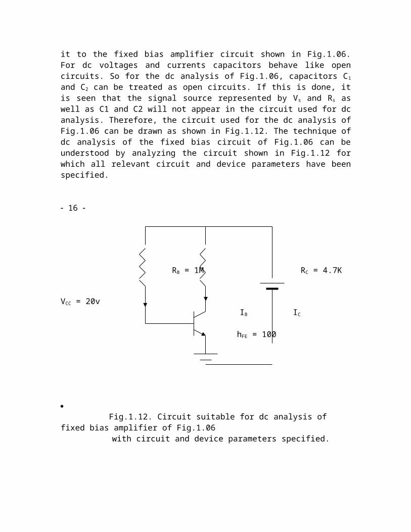
The techniques of dc analysis of amplifier circuits can be understood by applying it to the fixed bias amplifier circuit shown in Fig.1.06. For dc voltages and currents capacitors behave like open circuits. So for the dc analysis of Fig.1.06, capacitors C1 and C2 can be treated as open circuits. If this is done, it is seen that the signal source represented by Vs and Rs as well as C1 and C2 will not appear in the circuit used for dc analysis. Therefore, the circuit used for the dc analysis of Fig.1.06 can be drawn as shown in Fig.1.12. The technique of dc analysis of the fixed bias circuit of Fig.1.06 can be understood by analyzing the circuit shown in Fig.1.12 for which all relevant circuit and device parameters have been specified.
16
RB = 1M RC = 4.7K
VCC = 20v IB IC
hFE = 100
Fig.1.12. Circuit suitable for dc analysis of fixed bias amplifier of Fig.1.06
with circuit and device parameters specified. DC analysis of amplifier circuits also can be carried out using either (a) graphical method or (b) circuit analysis technique. It will be very useful, however, to define a few terms before the analysis is carried out.
Quiescent point Whenever the dc supply voltage VCC is switched on for the fixed bias circuit shown in Fig.1.12, voltages and currents settle down to steady state or dc or
quiescent values almost immediately. The steady state dc collector current IC and the corresponding collector-to-emitter dc voltage VCE across the transistor represent what is known as the quiescent operating point, or more concisely, the “quiescent point” of the device.
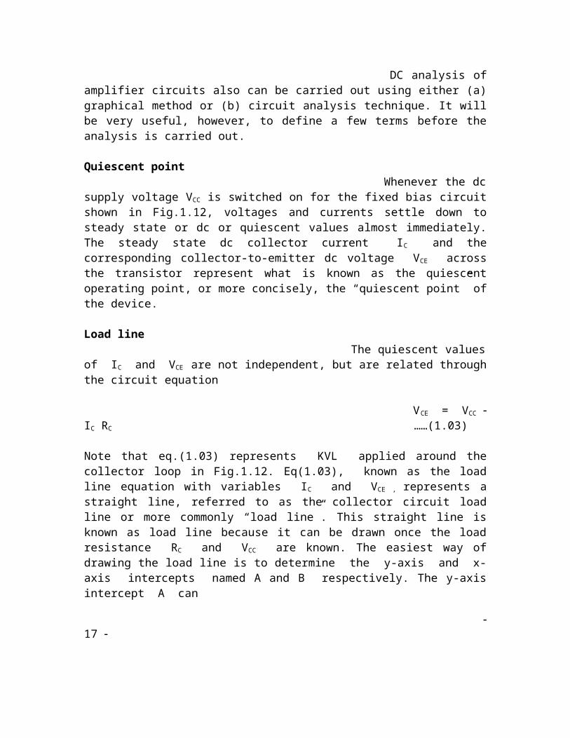
Load line The quiescent values of IC and VCE are not independent, but are related through the circuit equation
VCE = VCC IC RC ……(1.03)
Note that eq.(1.03) represents KVL applied around the collector loop in Fig.1.12. Eq(1.03), known as the load line equation with variables IC and VCE , represents a straight line, referred to as the collector circuit load line or more commonly “load line”. This straight line is known as load line because it can be drawn once the load resistance RC and VCC are known. The easiest way of drawing the load line is to determine the y-axis and x-axis intercepts named A and B respectively. The y-axis intercept A can
17
be obtained by reducing VCE to zero in eq.(1.03) which yields IC = VCC / RC . The x-axis intercept B can be obtained by reducing IC to zero in eq(1.03) which gives VCE
= VCC . If A is located on the y-axis at IC = VCC / RC and B is located on the x-axis at VCE = VCC and if A and B are connected by a straight line, as shown in Fig.1.13, the graphical representation of load line is obtained.
VCC A (Saturation point)RC
Load line
IC
B (Cutoff point)
VCE VCC
Fig.1.13. Graphical representation of eq.(1.03), i.e., load line.
Note that the load line equation, eq.(1.03), being a circuit equation, can be written in exactly the same form for any type of active device, if the variables IC and VCE are replaced by the corresponding device current ID and device voltage VD respectively. Obviously, the load line of Fig.1.03 can be drawn in exactly the same way without reference to the device, with only symbolic changes in the device variables, i.e., replacing the y-axis variable IC with ID and the x-axis variable VCE with VD.
(a) Graphical analysis of fixed bias amplifier circuit
The first phase of the graphical analysis of the fixed bias circuit of Fig.1.12 deals with the problem of locating the quiescent point or dc operating point of the device on the device characteristics. For this the first step is to draw the collector circuit load line as explained in connection with Fig.1.13, using numerical values of the
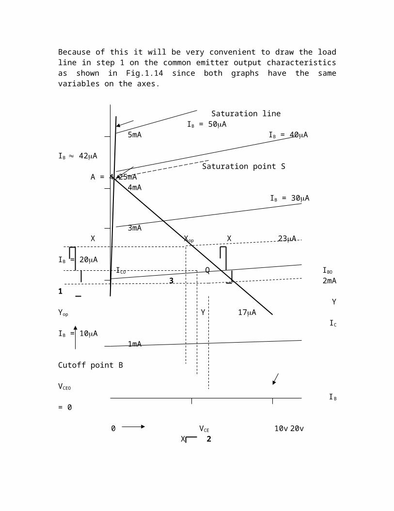
18 circuit parameters specified in Fig.1.12. For the parameters defined for this circuit, A, the intercept on the y-axis will be located at IC = VCC / RC = 20 / 4.7K = 4.25 mA and B, the x-axis intercept will be at VCE = VCC = 20v. If A and B are located on the respective axes and joined by a straight line the load line is obtained. This is shown in Fig.1.14.
The quiescent point ( V CEO , ICO ) must necessarily lie on the load line since VCEO and ICO must satisfy eq.(1.03), the load line equation. The exact location of the quiescent point on the load line is decided by the second constraint imposed by the device. The device constrains the quiescent point to lie on the device characteristic it is forced to operate by the circuit. Since the quiescent point must lie on the load line and also on a particular device characteristic, the intersection of these two lines will specify the location of the quiescent point. It is necessary to draw these two lines on the same graph to locate their point of intersection. Because of this it will be very convenient to draw the load line in step 1 on the common emitter output characteristics as shown in Fig.1.14 since both graphs have the same variables on the axes.
Saturation line IB = 50A 5mA IB = 40A IB 42A Saturation point S A = 4.25mA 4mA
IB = 30A
3mA X Xop X 23A IB = 20A
ICO Q IBO
3 2mA 1 Y Yop Y 17A
IC IB = 10A 1mA Cutoff point B VCEO
IB = 0
0 VCE 10v20v X 2
Y Fig.1.14. Load line drawn on transistor output characteristics. 19
The second step in the analysis is to locate the characteristics on which the transistor is constrained to operate by circuit . Each of the transistor characteristics shown in Fig.1.14 is plotted for a specific value of dc base current IB . If the dc base current of the transistor in Fig.1.12 is determined it will be possible to locate the characteristic in Fig.1.14 on which the quiescent point lies. The dc base current IBO
can be obtained graphically using the loop equation for the loop formed by RB , base-emitter junction and VCC . The loop equation can be written as
VCC = IB RB + VBE Or VBE = VCC IB RB ……….(1.04)
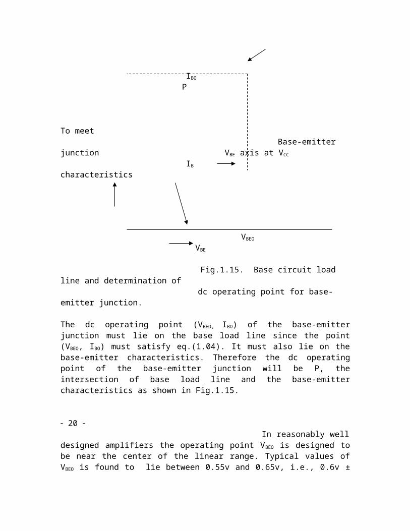
It is observed that eq.(1.04) has the same form as eq.(1.03), if VBE and IB are taken to be the variables similar to VCE and IC in eq.(1.03). Eq.1.04 can, therefore, be considered as the base circuit load line equation represented graphically in Fig.1.15
. Base circuit load line [ eq.(1.04) ]
VCC
RB
DC operating point IBO P
To meet Base-emitter junction VBE axis at VCC
IB characteristics
VBEO
VBE
Fig.1.15. Base circuit load line and determination of dc operating point for base-emitter junction.
The dc operating point (VBEO, IBO) of the base-emitter junction must lie on the base load line since the point (VBEO, IBO) must satisfy eq.(1.04). It must also lie on the base-emitter characteristics. Therefore the dc operating point of the base-emitter junction will be P, the intersection of base load line and the base-emitter characteristics as shown in Fig.1.15.
20 In reasonably well designed amplifiers the operating point V BEO
is designed to be near the center of the linear range. Typical values of VBEO is found to lie between 0.55v and 0.65v, i.e., 0.6v ± 50mv for silicon transistors. Therefore, in circuit analysis nominal value of base emitter dc voltage can be assumed to be 0.6v with little error since most of the commonly used transistors at present are silicon transistors. For example, if VBE is assumed to be 0.6v in eq.(3.02) and the numerical values of VCC and RB as given in Fig.1.12 are used IB is obtained as 19.4A 20A. It is expected that the graphical method shown in Fig.1.15 will yield a value for VBEO close to 0.6v and a value for IBO close to 20A. This means that the quiescent operating point must lie on the output characteristics corresponding to IB = 20A. Since the quiescent point must also lie on the load line, the intersection of load line and the characteristics for IB = 20A, i.e., the point marked Q in Fig.1.14 will be the quiescent point. At the quiescent point Q, the collector-to-emitter voltage VCE = VCEO will be around 11 volts and the collector current IC = ICO will be around 2.2mA as seen from Fig.1.14.
Graphical Analysis for ac signals The process of amplification of ac signals using, the circuit of Fig.1.06 with the parameter values specified in Fig.1.12, can be understood from the waveforms shown in Fig.1.14. When the supply voltage VCC = 20v is applied to the amplifier circuit shown in Fig.1.06 a dc base current IBO = 20A flows into the base terminal of the transistor. When a signal is applied to the circuit as shown in Fig.1.06 a signal current is also flows into the base along with the dc or quiescent base current of 20A. The total base current ib, according to superposition principle, will be the sum of the quiescent base current IBO and the signal current is and can be written as
Total base current ib = IBO is = 20A is ……(1.05)
The peak value of the signal current is in the base loop is assumed, arbitrarily, to be 3A. It must be realized, however, that a signal voltage Vs, typically of the order of a few millivolts, will be sufficient to send a current of the order of 3A in the base loop. According to eq.(1.05), this signal current added to the dc base
current IBO equal to 20A will make the total base current reach a maximum of 23A at the positive peaks of the signal and a minimum of 17A at the negative peaks. This base current waveform for the full cycle is shown graphically as waveform “1” in Fig.1.14.
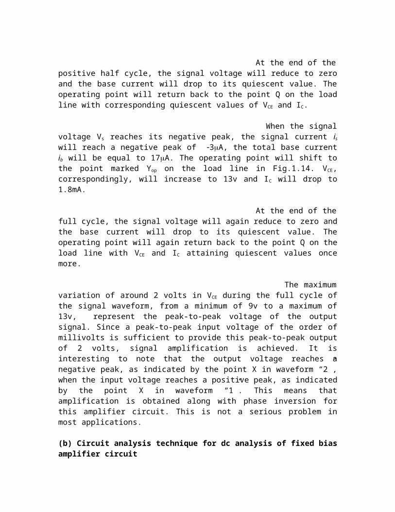
At the beginning of a cycle of signal voltage waveform is = 0 and the total base current ib will have a magnitude equal to its quiescent value of 20A as shown in waveform “1” of Fig.1.14. Since the operating point at that instant of time is at the intersection of the device characteristics for ib = IBO = 20A and the load line, it will be located at the quiescent point Q with VCE 11v and IC 2.2mA. This will correspond to the beginning point of the collector-to-emitter voltage waveform shown as waveform “2” in Fig.1.14 and the beginning point of the collector current waveform shown as waveform “3” in the same figure. 21
When the signal voltage reaches the positive peak, the signal current is in the base loop will reach a positive peak equal to 3A and the total base current ib will be equal to 23A. This will correspond to the point marked X in waveform “1” shown in Fig.1.14.The operating point at this ib will lie at the intersection of the device characteristics for 23A and the load line, i.e., at the point marked Xop on the load line in Fig.1.14. Corresponding to this VCE will drop to around 9v indicated by the point X in waveform “2” and IC will increase to around 2.6mA as shown by the point X in waveform “3”.
At the end of the positive half cycle, the signal voltage will reduce to zero and the base current will drop to its quiescent value. The operating point will return back to the point Q on the load line with corresponding quiescent values of VCE and IC. When the signal voltage V s reaches its negative peak, the signal current is will reach a negative peak of 3A, the total base current ib will be equal to 17A. The operating point will shift to the point marked Yop on the load line in Fig.1.14. VCE, correspondingly, will increase to 13v and IC will drop to 1.8mA.
At the end of the full cycle, the signal voltage will again reduce to zero and the base current will drop to its quiescent value. The operating point will again return back to the point Q on the load line with VCE and IC attaining quiescent values once more.
The maximum variation of around 2 volts in V CE during the full cycle of the signal waveform, from a minimum of 9v to a maximum of 13v, represent the peak-to-peak voltage of the output signal. Since a peak-to-peak input voltage of the order of millivolts is sufficient to provide this peak-to-peak output of 2 volts, signal amplification is achieved. It is interesting to note that the output voltage reaches a negative peak, as indicated by the point X in waveform “2”, when the input voltage reaches a positive peak, as indicated by the point X in waveform “1”. This means that
amplification is obtained along with phase inversion for this amplifier circuit. This is not a serious problem in most applications.
(b) Circuit analysis technique for dc analysis of fixed bias amplifier circuit
Circuit analysis technique means using methods of circuit analysis to analyse the amplifier circuit, replacing active devices by circuit models which will behave in exactly the same manner as the device. DC analysis means determination of dc voltages and currents at various points in the amplifier circuit when all the dc voltage and current sources connected with the circuit are activated. For dc analysis the device must be represented by a dc circuit model which will behave exactly as the device for dc voltages and currents. A different circuit model is to used for ac or signal analysis.
22 DC equivalent circuits or dc circuit models for bipolar junction transistors
It has been mentioned already that the forward voltage drop across the base-emitter junction of a silicon transistor operating in the linear region will be around 0.6v 50mv. Neglecting 50mv in comparison with 0.6v will, in general, cause negligible error in most dc analysis. For example, eq.(1.04) represents KVL applied to the base loop. From this equation IB can be written as
IB = …...(1.06)
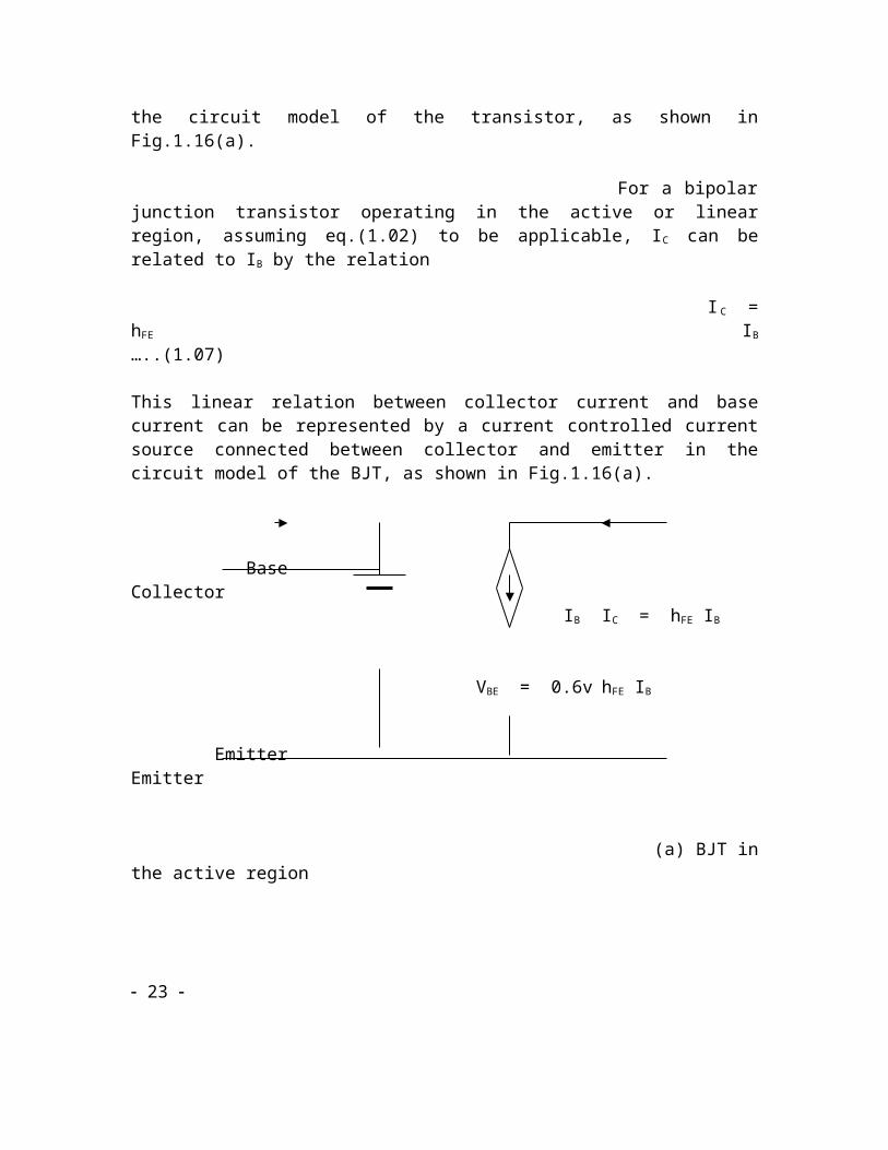
In the numerator of eq.(1.06) it will make very little difference whether VBE is taken as 0.6v or 0.6v 50mv, since VCC is usually quite large. So in most dc analysis VBE is taken to be a fixed voltage equal to 0.6v assuming the transistors to be made of silicon material. This fixed voltage of 0.6v between base and emitter can be represented by a 0.6v dc battery connected between base and emitter in the circuit model of the transistor, as shown in Fig.1.16(a).
For a bipolar junction transistor operating in the active or linear region, assuming eq.(1.02) to be applicable, IC can be related to IB by the relation
IC = hFE IB …..(1.07)
This linear relation between collector current and base current can be represented by a current controlled current source connected between collector and emitter in the circuit model of the BJT, as shown in Fig.1.16(a).
Base Collector IB IC = hFE IB
VBE = 0.6v hFE IB
Emitter Emitter
(a) BJT in the active region
23
Base Collector Base Collector
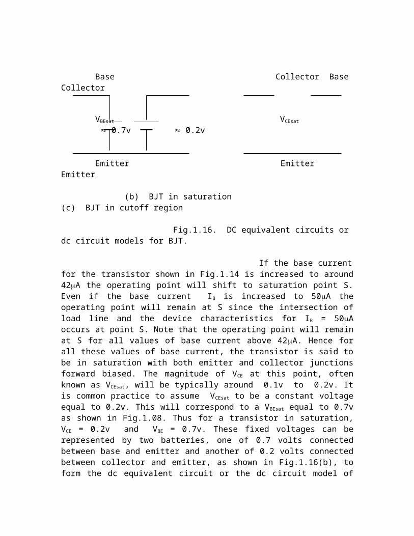
VBEsat VCEsat
0.7v 0.2v Emitter Emitter Emitter (b) BJT in saturation (c) BJT in cutoff region Fig.1.16. DC equivalent circuits or dc circuit models for BJT.
If the base current for the transistor shown in Fig.1.14 is increased to around 42A the operating point will shift to saturation point S. Even if the base current IB is increased to 50A the operating point will remain at S since the intersection of load line and the device characteristics for IB = 50A occurs at point S. Note that the operating point will remain at S for all values of base current above 42A. Hence for all these values of base current, the transistor is said to be in saturation with both emitter and collector junctions forward biased. The magnitude of VCE at this point, often known as VCEsat, will be typically around 0.1v to 0.2v. It is common practice to assume VCEsat to be a constant voltage equal to 0.2v. This will correspond to a VBEsat equal to 0.7v as shown in Fig.1.08. Thus for a transistor in saturation, VCE = 0.2v and VBE = 0.7v. These fixed voltages can be represented by two batteries, one of 0.7 volts connected between base and emitter and another of 0.2 volts connected between collector and emitter, as shown in Fig.1.16(b), to form the dc equivalent circuit or the dc circuit model of the transistor in saturation. It can be seen from Fig.1.16(b) that the collector-to-base junction is forward biased by a voltage equal to 0.5v for the transistor in saturation.
The collector current ICsat at S in Fig.1.14, where the transistor just enters saturation, and the y-intercept of load line at IC = A = VCC / RC differ by a negligible amount. So it is usual to equate these two and write ICsat = VCC / RC and

express the base current at the point of saturation IBsat = ICsat / hFE = VCC / hFE RC. Another way of obtaining the expression for ICsat is to write IC = (VCC VCE) / RC from eq.(1.03) and to modify it as ICsat = (VCC VCEsat) / RC at saturation. Since VCEsat of the order of 0.1v to 0.2v is negligible compared to VCC, collector current at saturation can be approximated as ICsat = VCC / RC.
A transistor in the cutoff region will have both collector and emitter junctions reverse biased with collector current as well as base current equal to zero. Therefore, if all the three terminals are left open as shown in Fig.1.16(c), it will form the dc equivalent circuit or dc circuit model of the transistor in the cutoff region.
24
Procedure for dc analysis of amplifier circuits using dc equivalent circuits
1. Assume (1 + hFE) ICBO << hFE IB. The approximation IC = hFE IB is then valid.2. Draw the amplifier circuit modified for dc analysis. (See, for example, Fig.1.12)3. Assuming the transistor to be in the active region, replace the transistor symbol by
its dc equivalent circuit for active region shown in Fig.1.16(a).4. Analyse the circuit to find out IB , IC and all the relevant voltages and currents. 5. Verify the validity of the two assumptions made in step 1 and step 3.
Sometimes the analysis might give odd results, such as a voltage drop across RC larger than VCC, which is not possible. This is usually an indication that the transistor might be in saturation. In such cases the analysis already done will have to be discarded and steps 3 and 4 will have to be repeated using dc equivalent circuit for the transistor in saturation shown in Fig.1.16(b).
Limitations of Practical Fixed Bias Amplifier Circuits
The main limitation on the performance of the fixed bias circuit arises from the fact that the manufacturers specify one of the widest tolerance ever for the hFE of the transistors they manufacture. The tolerance is so wide that instead of specifying it in terms of a percentage it is specified in terms of a minimum value, a typical value and a maximum value. In most cases the ratio of maximum value to minimum value of hFE is around 3, in some cases it increases to 5 or more and in a few cases it is limited to 2. The data sheets of the transistor BC 107, given in Appendix X, shows that for this transistor hFEmin = 110, hFEtyp = 180 and hFEmax = 220. Anyone attempting amplifier circuit design must make allowance for the fact that for any transistor that is selected for the circuit the hFE can lie anywhere between hFEmin and hFEmax .In contrast, shift in hFE due to temperature variations in low power amplifiers is much less. It has been shown that an amplifier will be able to give maximum peak-to-peak output without distortion if it is biased to operate with the quiescent point at the center of the load line. This objective will be attained only so long as the quiescent point remains at the center of the load line permanently. Since the hFE of the particular transistor used in the circuit can lie anywhere within
manufacturer’s tolerance, it is necessary to verify how far this shift in hFE , when changing the transistor in the circuit to another of the same type from the same manufacturer, will affect the location of quiescent point. If the quiescent point shifts beyond tolerable limits for change in hFE within manufacturer’s tolerance, a different type of biasing circuit should be used to guard against this.
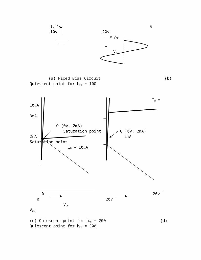
A specific example of fixed bias circuit design will clarify the problem. Assume that the transistor selected to be used in the fixed bias circuit, shown in Fig.1.17(a), has hFE specified as hFEmin = 100, hFEtyp = 200 and hFEmax = 300. To make the collector current IC independent of variations in ICB0 it is chosen to be 1mA so that IC >> ( 1 + hFE ) ICB0 and the expression for collector current IC , given in
25
VCC = 20v 2mA IB = 20A
RB Q (10v, 1mA) (1.94M) RC (10K)
1mA IC IB = 10A
IC = 1mA
hFE = 100 IB 0 10v 20v
VCE
V0
(a) Fixed Bias Circuit (b) Quiescent point for hFE = 100
IB = 10A 3mA
Q (0v, 2mA) Saturation point Q (0v, 2mA)
2mA 2mA Saturation point IB = 10A
0 20v 0 20vVCE VCE
(c) Quiescent point for hFE = 200 (d) Quiescent point for hFE = 300
Fig.1.17. Shift of quiescent point with change in hFE for a fixed bias circuit.
26
eq.(1.01), can be approximated as IC hFE IB . To dramatise the problem it is assumed that the design is carried out using hFE = hFEmin = 100. This choice of hFE makes IB
= IC hFE = 10A. With IB = 10A and VCC given as 20 volts, RB = 1.94 M from eq.(1.04), assuming a nominal value of 0.6 volts for VBE since most of the currently available transistors are made of silicon. Maximum undistorted peak-to-peak output voltage is obtained when the quiescent point Q is located at the center of the load line, i.e., when Q is located at ( 10v , 1mA ) as shown in Fig.1.17(b). Since quiescent V CE is to be 10 volts, voltage drop across RC will also be 10 volts, the supply voltage being 20 volts. The quiescent voltage drop of 10 volts across RC and the choice of collector current as 1mA will make RC = 10K. This completes the design of the circuit. The completed design is shown in Fig.1.17(a). With RC and VCC known, the load line can be drawn as shown in Fig.1.17(b). The intersection of load line and the device characteristics for quiescent base current IB = 10A locates the quiescent point Q shown in Fig.1.17(b). The output voltage waveform at the lower part of the figure shows that an undistorted output voltage of 20 volts peak-to-peak can be obtained from the circuit designed.
Assume that the transistor used in the circuit of Fig.1.17(a) and for the graph shown in Fig.1.17(b) worked well in the circuit for some time and became defective thereafter. The remedy is to replace the defective transistor with another having the same type number and from the same manufacturer. It is also stipulated that the new transistor used as a replacement for the old transistor has hFE = 200. Note that this hFE is well within the manufacturer’s tolerance. The quiescent base current for the new transistor also will be 10A, the same as the base current for the old transistor. The base current does not vary because IB = ( VCC VBE ) RB from eq.(1.04) and VBE depends only on the material used for making the transistor and not on the type or make of the transistor. Since quiescent value of IB , which is the bias current, is a constant independent of the transistor used, the circuit is called the ‘‘fixed bias circuit’’. The device characteristics for IB = 10A for the new transistor is shown in Fig.1.17(c). The intersection of this characteristic and the load line locates the quiescent point Q as shown in Fig.1.17(c). Note that the quiescent point is just at the point of saturation and, correspondingly, only one half of the input waveform is amplified as explained in connection with Fig.1.10. If the new transistor used as replacement for the original
transistor has hFE = 300, the upper limit of manufacturer’s tolerance, the bias current IB
will still remain at 10A and the quiescent point Q will be located at the point shown in Fig.1.17(d). As can be seen from the figure the quiescent point Q has gone well into saturation and, therefore, the circuit will amplify only less than half a cycle of the waveform. This shows that the circuit design is not satisfactory because it can cause defective operation when transistors are replaced.
27
hFE = 100 hFE = 200 hFE = 300 2mA 2mA 2mA 1.5mA Q (5v, 1.5mA) 1mA Q (10v, 1mA) 0.5mA Q (15v, 0.5mA)
0 15v 20v 0 10v 20v 0 5v 20v VCE VCE VCE
V0 V0 V0
10v 15v 20v 0v 10v 20v 0v 5v 10v
(a) If hFE shifts to 100 (b) For hFE = 200 (c) If hFE shifts to 300
Fig.1.18. Performance of optimal design of fixed bias circuit using hFE = hFEtyp = 200
A sensible way of overcoming this problem to some extent is to design the circuit with the typical value of hFE rather than the minimum or maximum value. If typical value of hFE = hFEtyp = 200 is used for the design, IC being 1 mA, IB = IC hFE = 5A and consequently RB = 3.88M. RC remains the same as before because the quiescent point is to be at the center of the load line with V CE = 10v. The load line, the device characteristics for IB = 5A and the quiescent point at the intersection of these two are shown in Fig.1.18(b). The waveform of the output voltage V0 , shown at the bottom of the figure, indicates that the circuit is able to provide an undistorted peak-to-peak output of 20 volts, the maximum possible from the circuit.
If the transistor in the circuit is replaced with another one having hFE = 100, the lower limit specified by the manufacturer, the quiescent point Q will shift to the point shown in Fig.1.18(a). The maximum undistorted output will be only 10 volts peak-to-peak in this case as shown in the figure. If the input is increased beyond this, the
positive peaks of the waveform will be clipped at VCE = 20v since VCE cannot increase beyond VCC . Similarly if the transistor is changed to another with hFE = 300, the upper limit specified by the manufacturer, the quiescent point Q will shift to the point shown in Fig.1.18(c). In this case also the maximum undistorted output will be 10 volts peak-to-peak as shown in the figure. If the input is increased beyond this, the negative peaks of the waveform will be clipped at VCE = 0 since VCE cannot reduce below 0 volts.
28
It is clear that if typical value of h FE is used for the design of a fixed bias circuit, the designer will be able to guarantee an undistorted peak-to-peak output voltage of the order of one half the supply voltage VCC for all values of hFE within the manufacturer’s tolerance. Because of this and the fact that only one extra resistance is required for biasing, the fixed bias circuit is very popular in amplifiers required to provide reasonably low values of output voltage. Front end amplifiers or initial stages of multistage high-gain amplifiers will be required to handle only very low values of signal voltages and in such cases the fixed bias circuit is very popular.
The h FE of a transistor can vary not only due to production tolerances but also due to temperature variations. Temperature variations in a transistor can be attributed in part to ambient temperature variations and in part to power dissipation in a transistor during operation. Assuming an ambient temperature variation of 25oC around an average temperature of 25oC and approximately 5oC rise in temperature above ambient due to power dissipation as explained in chapter X, the total temperature variation can be taken to be between 5oC and 55oC, i.e., 25oC around an average level of 30oC. The graph of hFE plotted against IC , shown in Fig.1.19, indicates that a variation in temperature of the order of 30oC around 30oC causes only around 20% variation in hFE . This indicates that the shift in magnitude of hFE in a circuit is mainly due to variation within manufacturer’s tolerance when transistors are replaced and not due to temperature variation.
200
150
hFE 150oC 100
60oC
50 0oC
55oC
0 5 IC 10 15
Fig.1.19. Variation of hFE with IC for different temperatures.
29
Analysis and Design of Biasing Circuits Most Frequently Used
In fixed bias circuits the quiescent or dc base current which represents the bias current, is independent of the transistor used. This is evident from eq.(1.06) in which the only parameter pertaining to the transistor pertains, strictly speaking, to the material of the transistor rather than the type of transistor used. For all silicon transistors, the most common type, VBE can be assumed to be 0.6 volts. IB being ‘fixed’ by the circuit parameters and material of the transistor, the quiescent current I C ( IC = hFE IB) and, consequently, the location of the quiescent point, varies in direct proportion to hFE . This is reflected in the position of the quiescent point in the three graphs of Fig.1.18. Because of this the circuit designer will be able to guarantee an undistorted peak-to-peak output voltage less than half the supply voltage. When output voltages comparable to the supply voltage VCC is required, fixed bias circuit will not be able to guarantee it. To overcome this problem other types of biasing circuits are used. In all the biasing circuits used, the primary purpose is, of course, to provide the bias current required so that the full waveform of the signal is reproduced properly. The secondary purpose is to stabilize, as far as possible, the quiescent collector current and, in turn, the quiescent point. The collector current IC in such circuits is a function of hFE , VBE and ICB0 , i.e., IC = f (hFE , VBE
, ICB0). The purpose of present analysis is to obtain expressions for collector current in terms of these variables. Using these expressions for IC , a logical approach to the design of biasing circuits is suggested.
It has been explained in connection with Fig.1.05(b) that a bias current for the transistor can be obtained by connecting a bias resistor between the base of the transistor and a point where there is a reasonably high positive dc voltage such as the + VCC dc supply bus. If the bias resistor is connected between the base of the transistor and the dc supply, the resulting circuit will be the fixed bias circuit shown in Fig.T.1.1.01 of Table.1.1. The bias resistor can also be connected between the base and the collector terminal since the dc voltage at the collector is expected to be around half the supply voltage. If the bias resistor is connected between the base and the collector, the collector-to-base bias circuit shown in Fig.T.1.1.02 of Table.1.1 is obtained. If a resistor is connected between the emitter terminal and ground in a fixed bias circuit some amount of negative feedback is introduced which will stabilize collector current to some extent. This type of bias is known as emitter bias shown in Fig.T.1.1.03 of Table.1.1. If the base resistor in an emitter bias circuit is connected to the collector instead of the + VCC supply as shown in Fig.T.1.1.04 of Table.1.1, the resulting circuit will be a combination of collector-to-base bias and emitter bias named collector-to-base cum emitter bias. If the base of the transistor is connected to the center of a voltage divider across the + V CC
supply and a resistor connected from emitter terminal to ground, the resulting circuit is

the voltage divider bias circuit shown in Fig.T.1.1.05 of Table.1.1. The biasing circuit termed VBE multiplier bias, shown in Fig.T.1.1.06 of Table.1.1 uses the transistor to simulate a zener diode for stabilizing the quiescent point. Note that in collector-to-base bias, collector-to-base cum emitter bias and VBE multiplier bias circuits the transistor will not go into saturation even if the resistor between collector and base is reduced to zero because in such a case VCE = VBE = 0.6v , which is larger than VCEsat 0.2v. 30
Table.1.1. Most Frequently Used Biasing Circuits Biasing circuit Expression for collector current
1. Fixed bias
+ VCC
RB RC
IC
IB
Fig.T.1.1.01. Fixed bias circuit
2. Collector-to-base bias
+ VCC
RC
RB IC + IB
IC
IB
Fig.T.1.1.02. Collector-to-base bias circuit
31
3. Emitter bias
+ VCC
RC
RB
IC
IB
RE
Fig.T.1.1.03. Emitter bias circuit
4. Collector-to-base cum emitter bias
+ VCC
RC
RB
IC + IB
IC
IB
RE
Fig.T.1.1.04. Collector-to-base cum emitter bias 32
5. Voltage divider bias
+ VCC
R1 RC
IC
IB
R2 RE
VCC R2
where, RTH = R1 R2 and ETH = R1 + R2
6. VBE multiplier bias
+ VCC
RC
R1
I + IC
I IC
IB
R2 +
VBE
Fig.T.1.1.06. VBE multiplier bias circuit
33
All the six biasing circuits shown in Table.1.1 can provide the bias current required. The fixed bias circuit provides no stability for the quiescent point as explained earlier. The collector-to-base bias, the emitter bias and the collector-to-base cum emitter bias provide varying degrees of stability for the collector current and the quiescent point. The voltage divider bias and the VBE multiplier bias can provide reasonably good stability for the collector current and the quiescent point through careful design.
The first step in the design of biasing circuits is to obtain expressions for collector current IC in terms of the variables hFE , VBE and ICB0 . For the
fixed bias circuit, the base current is given by eq.(1.06) which substituted in eq.(1.01) gives the required expression for IC given in Table.1.1. One way to analyse the biasing circuits of Fig.T.1.1.02 collector-to-base bias, Fig.T.1.1.03 emitter bias and Fig.T.1.1.04 collector-to-base cum emitter bias shown in Table.1.1 is to write the loop equation for the loop containing the base-emitter voltage and the VCC supply. The loop equation for such a loop in the case of emitter bias of Fig.T.1.1.03, for example, is given by
IB RB + VBE + ( IB + IC ) RE = VCC ……..(1.08)
Eliminating IB between eq.(1.08) and eq.(1.01), the expression for IC given in Table.1.1 is obtained.
The analysis of the voltage divider bias circuit shown in Fig.T.1.1.05 of Table.1.1 will be simpler if a different approach is used. The first step in the analysis is to redraw the circuit as shown in Fig.1.20(a). Note that this circuit which is
R1 RC RC
VCC VCC RTH = R1 R2 VCC
IB IB
ETH = VCC R2
R2 RE
R1+ R2 RE
(a) Fig.T.1.1.05 redrawn (b) Modification of (a) using Thevenin’s theorem
Fig.1.20. Modification of voltage divider bias circuit of Fig.T.1.1.05 for analysis
34
drawn with slight modification of the voltage divider bias circuit, will have the same voltage and current at all points as the original circuit. This is due to the fact that in the redrawn circuit also the upper end of both resistors R1 and RC has the same voltage VCC as the original circuit. The second step is to replace the circuit to the left of the dotted line by its Thevenin equivalent as shown in part (b) of the figure. Thevenin voltage E TH of the equivalent circuit will be [VCC R2] [R1 + R2] and Thevenin resistance RTH will be [R1 R2] = [R1 R2] [R1 + R2]. The loop equation for the base loop can be written as
ETH = IB RTH + VBE + (IB + IC) RE ……..(!.09)
Eliminating IB between eqs.(1.09) and (1.01) the expression for collector current IC for the voltage divider bias circuit, given in Table.1.1, is obtained.
The V BE multiplier bias circuit uses the transistor to simulate a zener diode. A good understanding of this type of bias can be obtained by an analysis of the BJT circuit which simulates a zener diode.
VBE multiplier : Use of BJT as a zener diode
A A I = IR1 + IC
R1 IC
IR1 = IR2 + IB R1 + R2
IB VZ = VBE
R2
IR2 = VBE R2
R2
B B
(a) BJT connected as a VBE multiplier (b) Equivalent zener diode
35
Q
R
I
P
O VAB VBE (R1 + R2) R2
(c) Current – Voltage relation of the VBE multiplier
Fig.1.21. A BJT circuit which simulates a zener diode
If a BJT is connected as shown in Fig.1.21(a), the circuit will behave like a zener diode shown in part (b) of the figure. This can be demonstrated as follows. If VAB is increased slowly from zero, initially the voltage will be too small for the base-emitter junction to conduct, the transistor will be cut off and only a resistance equal to (R1 + R2) will appear between terminals A and B. In this range the current I will vary with voltage VAB as shown by the straight line OP in Fig.1.21(c). When VAB is large enough for the base-emitter junction to conduct and bring the transistor to the edge of the active region,
VAB = ( IR2 + IB ) R1 + IR2 R2 = IR2 ( R1 + R2 ) + IB R1 ……..(1.10)
If, by design, IB << IR2 , i.e., ( IC hFE ) << ( VBE R2 ) ,
VAB IR2 ( R1 + R2) = VBE ( R1+ R2 ) = VZ ……..(1.11) R2
Eq.(1.11) shows that once the transistor enters the active region VAB tends to remain constant at VBE ( R1 + R2 ) R2 . Any attempt to increase VAB above this value will result
36
in abnormally high values of current and, unless this current is limited to safe values by an external series resistance, it will cause destruction of the transistor. In the active region of the transistor, where VAB remains constant, the current-voltage relation of the circuit can be represented by the vertical straight line PQ shown in Fig.1.21(c).
Since the transition from cutoff to conduction for a transistor takes place by a gradual rather than an abrupt increase in current when VBE is increased, the current-voltage relation for a practical VBE multiplier circuit will exhibit a rounded knee as shown by the dotted line in Fig.1.21(c) rather than the sharp corner formed by the firm lines OP and PQ. Moreover, for a transistor operating in the active region, there is a small increase in VBE with increasing current and this manifests itself as a tilt in the characteristics above the knee as shown by the dotted line in Fig.1.21(c). In this region the slope or dynamic resistance of the VBE multiplier, defined as VAB I , is typically of the order of 5 to 10. This is lower than that of a zener diode for which the dynamic resistance is around 10 to 15. Note that VZ , the ‘‘breakdown voltage’’ of the VBE
multiplier circuit exhibits a temperature coefficient equal to the temperature coefficient of VBE multiplied by (R1 + R2) R2 as per eq.(1.11), i.e., 2.5 (R1 + R2) R2 mV oC. The nominal value of VBE being 0.6v, this will represent a temperature coefficient of
50mV oC if VZ = 12v. VZ for this circuit corresponds to the quiescent voltage for the amplifier circuit. A 25oC temperature shift from the average value will cause a 1.25v shift in the quiescent voltage. This order of shift in quiescent voltage can be accommodated easily, if necessary, while designing the circuit.
The lowest breakdown voltage VZ attainable with this circuit is VBE 0.6v when R1 is zero and R2 is infinite. The maximum value of VZ is restricted to the collector-to-emitter breakdown voltage of the transistor. In all cases the power dissipation in the transistor, given by the product VAB . IC , must be restricted to the maximum power dissipation rating of the transistor.
RA A
RB
RC
RD B
Fig.1.22. A VBE multiplier with variable breakdown voltage VZ
37
The breakdown voltage V Z of the VBE multiplier circuit can be made variable using the arrangement shown in Fig.1.22. In this circuit R1 = RA + RB and R2 = RC + RD . The knee of the characteristics shown in Fig.1.21(c) can be made sharper and the slope resistance in the breakdown or active region decreased for the VBE
multiplier circuit by using a Darlington pair or complementary Darlington pair of transistors instead of a single transistor.
Simplified Analysis of the VBE multiplier Bias Circuit
In VBE multiplier bias circuit the collector-to-emitter voltage VCE
and, consequently, the quiescent point can be designed to be stable against variations in hFE and ICB0 but not against variations in VBE. This can be demonstrated as follows. For the circuit shown in Fig.T.1.1.06,
VCE = VCC ( I + IC ) RC ……..(1.12)
and also VCE = VBE + I R1 ……..(1.13)
Equating eqs.(1.12) and (1.13)
I ( RC + R1 ) + IC RC = VCC VBE ……..(1.14)
From Fig.T.1.1.06
IB = I VBE ……..(1.15) R2
Using the approximate relation, IC hFE IB and using eq.(1.15) for IB
IC hFE IB = hFE I hFE VBE ……..(1.16) R2
Substituting eq.(1.16) in eq.(1.14),
[ VCC VBE + hFE VBE ( RC R2 ) ] ……..(1.17) I =
R1 + (1 + hFE ) RC
Substituting eq.(1.17) in eq.(1.13),
VCC R1 + VBE RC + hFE RC R1
(1 + hFE) (1 + hFE) R2
VCE = ……..(1.18) RC + [ R1 (1 + hFE) ]
38
In eq.(1.18) [ h FE (1 + hFE) ] can be approximated to unity with little error and if [ R1 (1 + hFE) ] is designed to be small compared to RC , eq.(1.18) can be written as
VCE VCC R1 1 + VBE 1 + R1 ……..(1.19) (1 + hFE) RC R2
Designing [ R1 (1 + hFE) ] << RC , which implies [ R1 (1 + hFE) RC ] << 1 , the first term on the right hand side of eq.(1.19) can be neglected. Then
VCE VBE R1 + R2 ……..(1.20) R2
Note that eq.(1.20) is the same as eq,(1.11). Eq.(1.20) shows that VCE is equal to VBE
multiplied by a factor equal to [ ( R1 + R2 ) R2 ] for this circuit and this bias circuit is named accordingly. However, the temperature coefficient of VCE will be equal to the temperature coefficient of VBE ( which is 2.5 mV oC ) multiplied by [ ( R1 + R2 ) R2 ]. Normally the quiescent voltage VCE will be designed to be of the order of VCC 2 and,
correspondingly, [ ( R1 + R2 ) R2 ] will be of the order of 20 and the temperature coefficient of VCE will be around 50 mV oC. This will result in a 1.25 volt shift in quiescent voltage when temperature changes by 25oC. This order of variation is not very significant and can be easily accommodated in the design if necessary.
The analysis carried out for the V BE multiplier circuit as well as the VBE multiplier bias circuit assumes that IC >> (1 + hFEmax) ICB0max , the terms involving ICB0 are neglected and the approximation IC hFE IB is used. ICB0 terms do not appear, therefore, in the expressions for IC and VCE and the effects of ICB0 variations on IC and VCE
cannot be assessed using these expressions. The full expression for IC involving hFE , VBE
and ICB0 for the VBE multiplier bias, given in Table.1.1, can be obtained from eqs.(1.01), (1.14) and (1.15) by eliminating IB and I between these three equations.
It is essential to note the in deriving the equations given in Table.1.1 the exact expression given in eq.(1.01) has to be used. The approximate expression given in eq.(1.02) should not be used at all for this analysis.
39
Design of Biasing Circuits for Single Transistor Amplifiers
The Primary purpose of biasing is to provide a biasing current to the transistor so that the full waveform of the signal is reproduced properly. The secondary purpose of biasing circuits is to provide stability of quiescent point to the extent possible. The quiescent voltage and current are related to each other through the load line equation so that stabilizing one will automatically stabilize the other. The attempt in the design will be to stabilize the quiescent collector current IC of each circuit as much as possible.
The biasing circuits and expressions for collector current given in Table.1.1 is the starting point of the design. The collector current is, in general, a function of hFE , VBE and ICB0 as shown by the expressions for IC given in Table.1.1. The design should attempt to stabilize IC against variations in each of these three parameters.
Stabilisation of IC Against Variations in ICB0
In all the six equations for IC given in Table.1.1 only the last term involves ICB0 . Since ICB0 is quite sensitive to temperature a satisfactory method of stabilizing IC against variations in ICB0 is to make the last term in each equation negligibly small compared to IC . In other words, stabilisation of IC against variations in ICB0 can be achieved by designing IC to be large compared to the last term in each equation. To do this the largest possible value of the last term in each case has to be evaluated. The equations indicate that the last term can be evaluated only if the circuit parameters are
known, i.e., after the design is completed. This difficulty can be resolved as follows. Note that the last term in each of these equations is of the form (1 + hFE) ICB0 (1 + K) , where K is a positive real quantity equal to or larger than zero. This means that the denominator of the last term in all the equations is a quantity equal to or larger than unity. Among the six equations the largest value for the last term is for the fixed bias circuit for which K = 0 and the last term equal to (1 + hFE) ICB0 . If the largest possible value of this expression is determined and IC chosen to be large compared to it, IC will be large compared to the last term for all the six equations. Largest value of (1 + hFE) ICB0 corresponds to the largest value of both hFE and ICB0 . The maximum value of hFE can be obtained from the data sheets of the transistor supplied by the manufacturer. The maximum value of ICB0
can be evaluated as follows.
ICB0 , the reverse saturation current of the collector-to-base junction of the transistor with emitter open, doubles for every 10oC rise in temperature. An expression for ICB0 as a function of collector junction temperature Tj can be written as
= ICB0ref ……..(1.21)
40
where, ICB0 (Tj) is the magnitude of ICB0 at any arbitrary collector junction temperature Tj and ICB0ref is the magnitude of ICB0 at a reference collector junction temperature Tjref
specified by the manufacturer. The data sheets of the transistor BC 107, given in Appendix X, specifies ICB0 to be less than 15A at 150oC so that for this transistor ICB0ref = 15A and Tjref = 150oC. If a maximum ambient temperature of 55oC is assumed and a further increase of 5oC in collector junction temperature due to power dissipation in the transistor is estimated, the maximum possible junction temperature can be taken to be 60oC. Corresponding to a maximum junction temperature of 60oC and the specifications of the transistor indicated above, ICB0max the maximum value of the collector junction reverse saturation current for BC 107, calculated using eq.(1.21), will be 29.3nA. hFEmax for BC 107A is specified as 220 in the data sheets. Using this value of hFEmax the maximum value of (1 + hFEmax) ICB0max is calculated as 6.45A. The data sheets also shows that the BC 107B and BC 107C has hFEmax equal to 450 and 800 respectively. For hFEmax equal to 450 and 800 the maximum value of (1 + hFEmax) ICB0max is obtained as 13.2A and 23.4A respectively. If IC is chosen to be greater than about 0.5mA it will make IC >> (1 + hFEmax) ICB0max and variations in ICB0 will have negligible effect on IC .
Conclusion :
A choice of IC 0.5mA will stabilize IC against variations in ICB0 for all the six biasing circuits shown in Table.1.1.
Stabilisation of IC Against Variation in hFE

The h FE of the transistor, inserted into the circuit after the design is completed, can take any value between hFEmin and hFEmax specified by the manufacturer. For most transistors hFEmin and hFEmax are separated by a ratio 1:3. In many cases the ratio is larger and in a few cases it is smaller. The main reason for variation in hFE of the transistor used in any circuit is the wide tolerance specified by the manufacturer. The change in hFE due to ambient temperature variation and temperature variation due to power dissipation in the transistor in low power circuits is less significant.
The effect of h FE variation on IC is assessed assuming that the first part of the design has been completed and IC has been stabilized against variation in ICB0 by rendering the last term negligible by design in all the six equations for IC given in Table.1.1. If the last term in the expression for IC is rendered negligible the expression for collector current IC for the fixed bias circuit becomes directly proportional to hFE . This means that the fixed bias circuit cannot be stabilized against variations in hFE. However, the circuit can be used to good effect if the design is carried out using the typical value of hFE and possible shifts in quiescent point corresponding to shift in hFE within manufacturer’s tolerance is accepted.
41 The expressions for I C for collector-to-base bias, emitter bias and collector-to-base cum emitter bias circuits show that hFE occurs in the numerator as well as the denominator of the first term. This means that these circuits provide varying degrees of stability of IC with respect to hFE variations and are better than the fixed bias circuit in this respect. A satisfactory way of designing these circuits is to use the typical value of hFE for their design, as was recommended for the fixed bias circuit, and accept any possible shifts in the quiescent point due to variations in hFE .
The voltage divider bias circuit can be designed to provide very good stability for IC with respect to hFE variations as shown below. The expression for collector current IC for the voltage divider bias circuit, given in Table.1.1, with the last term rendered negligible by design, can be written as
= ……..(1.22)
where, = and = . If RTH is designed to be
small compared to (1 + hFE)RE , the denominator of eq.(1.22) can be approximated to (1 + hFE)RE and the equation can be written as
= ……..(1.23)
hFE is usually larger than 100 and hFE (1 + hFE) can be approximated to unity with less than 1% error. With this approximation eq.(1.23) reduces to
= ……..
(1.24)
The expression given in eq.(1.24) for IC is independent of hFE . This shows that making RTH << (1 + hFE)RE stabilizes IC against variations in hFE for voltage divider bias circuits. This condition for stability has to be satisfied even for the lowest value of h FE . So the stability condition is usually written as RTH << (1 + hFEmin)RE . Once the stability condition is satisfied the voltage drop across RTH becomes negligible and, as seen from Fig.1.20(b), the voltage drop between the base terminal and ground can be approximated to ETH . This means that for normally expected variations in base current the voltage at the base terminal remains constant at ETH , the voltage across R2 . Fig.1.20(a) shows that the voltage across R2 remains constant at ETH = [VCC R2] [R1 + R2] for all values of IB
only if IBmax is negligible compared to the current through R1 and R2 . A different way of expressing the stability condition is to specify IBmax << IR1 IR2 . Stability condition expressed this way is very often more useful for designing certain types of circuits.
42 The expression for IC , given in table.1.1, for VBE multiplier bias shows that, with the last term rendered negligible by design, the first term will be independent of hFE if R1 << (1 + hFE)RC . Eq.(1.20) shows that the same condition will make the quiescent voltage VCE independent of hFE . Obviously, this condition for stability has to be satisfied even for the minimum value of hFE . So the stability condition is usually expressed as R1 << (1 + hFEmin)RC
Conclusion :
The collector current of fixed bias, collector-to-base bias, emitter bias and collector-to-base cum emitter bias circuits cannot be stabilized against variations in hFE . A satisfactory way of designing them will be to complete the design using typical value of hFE .
The collector current of voltage divider bias circuit can be stabilized against variations in hFE by making RTH << (1 + hFEmin)RE or RTH = (1 K) (1 + hFEmin)RE , where, a value of K equal to or larger than 10 is usually satisfactory.
For the VBE multiplier bias circuit the collector current can be stabilized against variations in hFE by making R1 << (1 + hFEmin)RC .
Stabilisation of IC Against Variations in VBE
The base-emitter junction voltage changes with temperature at the rate of 2.5mV oC. If the ambient temperature variation is assumed to be 25o 25oC and a further temperature rise of 5oC above ambient is assumed for the collector junction due to power dissipation in the transistor, the collector junction temperature T j can be expressed as 30o 25oC. Corresponding to this the base-emitter voltage can be
expressed as VBE0 VBE , where VBE0 is the base-emitter voltage at the average temperature and VBE is the change in base-emitter voltage corresponding to 25oC temperature variation. A nominal value of 0.6v is assumed for VBE0 in the case of silicon transistors and VBE corresponds to 62.5mV for a temperature variation of 25oC.
For the first four biasing circuits of Table.1.1 the expression for IC contains VBE in the form (VCC VBE0 VBE). Since VCC VBE0 is usually of the order of 10 volts or more and VBE has been estimated to be 62.5mV , the term (VCC VBE0 VBE) will show negligible variation corresponding to a change in base-emitter voltage VBE of the order of 62.5mV. This means that the quiescent point of the first four circuits in Table.1.1 are inherently stable against variations in VBE .
The expression for collector current I C for the voltage divider bias circuit, after stabilization with respect to ICB0 and VBE , is given by eq.(1.24). This expression can be stabilized against VBE , the change in base-emitter voltage, by making VBE << (ETH VBE0). Stabilisation with respect to hFE variations makes base-to-ground
43 voltage approximately equal to ETH as indicated earlier. Fig.1.20 shows that (ETH VBE0) represents the voltage drop VRE across the emitter resistance RE at the average temperature. The stability condition for IC against variations in VBE can be expressed as VBE << VRE . The change in base-emitter voltage VBE has been estimated as 62.5mV. Therefore, if VRE >> 62.5mV the voltage divider bias circuit will be stabilized against variations in VBE . A choice of VRE of the order of 0.6v to 2v is usually satisfactory. A higher VRE will provide better stability, but it will reduce the peak-to-peak undistorted output available from the circuit. If eq.(1.24) is stabilized with respect to VBE by making its variable part VBE << ( ETH VBE0 ) it reduces to
= ……..(1.25)
IC given by eq.(1.25) is independent of variations in ICB0 , hFE and VBE as required.
Eqs.(1.11) and (1.20) show that the quiescent voltage V CE for the VBE multiplier bias circuit is given by the expression
……..(1.26)
Eq.(1.26) shows that the quiescent voltage VCE will have a temperature coefficient equal to the temperature coefficient of VBE multiplied by [(R1 + R2) R2] . For a temperature variation of 25oC the quiescent voltage will vary by 62.5 mV multiplied by [(R1 + R2) R2] . This variation is typically of the order of 1.25 volts if VCE is designed to be around 12v. This order of variation is not very serious in amplifier circuits.
Conclusion :

The collector current IC for fixed bias, collector-to-base bias, emitter bias and
collector-to-base cum emitter bias circuits are inherently stable against variations in VBE .
The collector current IC for the voltage divider bias circuit can be stabilized against variations in base-emitter voltage if VRE >> VBE ( 62.5mV ). A value of VRE between 0.5v and 2v is usually satisfactory.
The VBE multiplier circuit is reasonably stable against variations in VBE .
Steps for Designing the Biasing Circuits
The steps for designing the six biasing circuits given in Table.1.1 can be written in three different sets. The first set of steps is a common set suitable for designing the first four biasing circuits given in Table.1.1, namely, the fixed bias, collector-to-base bias, emitter bias and collector-to-base cum emitter bias circuits. The second set of steps is specifically written for the voltage divider bias circuit and a third set specifically for the VBE multiplier bias circuit.
44
Steps for designing fixed bias, collector-to-base bias, emitter bias and collector-to-base cum emitter bias circuits.
1. Select IC to be larger than or equal to 0.5mA. [This will stabilize IC against variations in ICB0]
2. If emitter resistance RE is present in the circuit, select VRE , the voltage across it to be around 0.5 to 2 volts. [Larger values of VRE will improve quiescent point stability and increase input resistance. However, higher values of VRE will tend to reduce the amplitude of undistorted output available from the circuit].
3. Once VRE and IC is known, RE can be calculated as RE = VRE IE VRE IC for circuits for which RE is present.
4. Choose the quiescent voltage VCE to be VCC 2 .5. Calculate VRC , the voltage across RC as (VCC VCE VRE)6. Calculate RC = VRC IC .7. Calculate RB to provide the value of IC chosen in step 1. For this calculation the
first term in the expressions for IC given in Table.1.1 is used in which typical value of hFE is inserted, VBE0 is assumed to be 0.6 volts and VBE is neglected.
Steps for designing the voltage divider bias circuit
1. Select IC to be larger than or equal to 0.5mA. [This will stabilize IC against variations in ICB0].
2. Choose VRE , the voltage across the emitter resistance to be around 0.5 to 2 volts. [Larger values of VRE will improve quiescent point stability and increase input resistance. However, larger values of VRE will tend to reduce the amplitude of undistorted output available from the circuit].
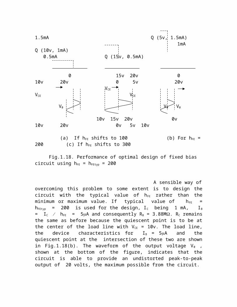
3. Once VRE and IC is known, RE can be calculated as RE = VRE IE VRE IC .4. Choose quiescent voltage VCE to be VCC 2 .5. Calculate VRC , the voltage across RC as (VCC VCE VRE).6. Calculate RC = VRC IC .7. Calculate ETH (VRE + VBE0) = (VRE + 0.6v).8. Calculate R1 and R2 from the two equations
and or
where, K is a large number. A choice of K 10 is usually satisfactory for the
design. Higher values of K provides better stability for quiescent point with respect to hFE variations. However, the lower values of input resistance resultingfrom higher values of K is a drawback.
45
Steps for designing the VBE multiplier bias
1. Select IC to be larger than or equal to 0.5mA. [This will stabilize IC against variations in ICB0].
2. Choose quiescent voltage VCE to be VCC 2.3. Calculate VRC , the voltage across RC as (VCC VCE) = VCC 2.4. Calculate RC = VRC IC = VCC 2 IC .5. Select R1 << (1 + hFEmin) RC . Low value of R1 reduces input resistance.6. Choose quiescent voltage VCE = VCC 2.7. Calculate R2 from eq.(1.26)
VBE is assumed to have a nominal value equal to 0.6 volts.
Choosing the collector current
The minimum collector current of about 1mA suggested in all these designs will normally provide a frequency response extending to a few MHz . A collector current of around 1mA will keep the current drain from the power supply to a low value and is satisfactory for all low frequency applications. If the frequency response is to be extended further the collector current will have to be increased and the increased current drain from the power supply accepted. Corresponding to this increase in IC there will be a decrease in the magnitude of resistances in the circuits. This will make the charging and discharging of device and wiring capacitances in the circuit faster due to reduced time constants and result in improvement of frequency response to the limit set by the device. A current of the order of 10mA is very often used in high frequency
amplifier circuits. A higher collector current of this order will also improve the high frequency performance of the BJT.
Voltage divider bias circuit as a constant current circuit
Eq.1.25 shows that for a voltage divider bias circuit the collector current IC can be designed to be a constant, independent of variations in ICB0 , hFE and VBE . Since ETH = [(VCC R2) (R1 + R2)] the collector current is seen to be independent of RC also. Even if the collector resistance is replaced by a short circuit so that RC = 0, the collector current remains the same with VCE = VCC . When RC is increased from zero to finite values IC remains constant and VCE decreases below VCC . As RC is increased continuously IC stays constant and VCE decreases steadily till the transistor is saturated, beyond which eq.(1.25) is no longer valid. This shows that as far as the collector load resistance is concerned the voltage divider bias circuit behaves like a constant current circuit so long as the transistor remains in the active region. Voltage divider bias circuit as a constant current circuit finds many uses such as differential amplifier circuits, analogue dc voltage regulators, emitter-coupled multivibrators, etc. 46
Building a JFET Amplifier
The amplifying behaviour of the JFET can be characterized by its voltage-to-current transfer characteristics expressed as
……..(1.27)
where, IDS is the drain current, IDSS the saturation drain current with VGS = 0, VGS the gate-to-source voltage and VP the pinch off voltage of the JFET. The parameters IDSS and VP
for the FET s are specified by the manufacturer.
Since the input voltage V GS of the JFET controls its output current IDS , it should be possible to construct an amplifier using this transistor. The first step in constructing an amplifier using a JFET is to interconnect the signal source, represented as a Thevenin source, and the transistor in such a way that a voltage VGS
proportional to the source voltage VS appears between the gate and source terminals of the JFET. A logical way of doing this is to connect the signal source between the gate and source terminals of the transistor as shown in Fig.1.23(a).
RD
RS
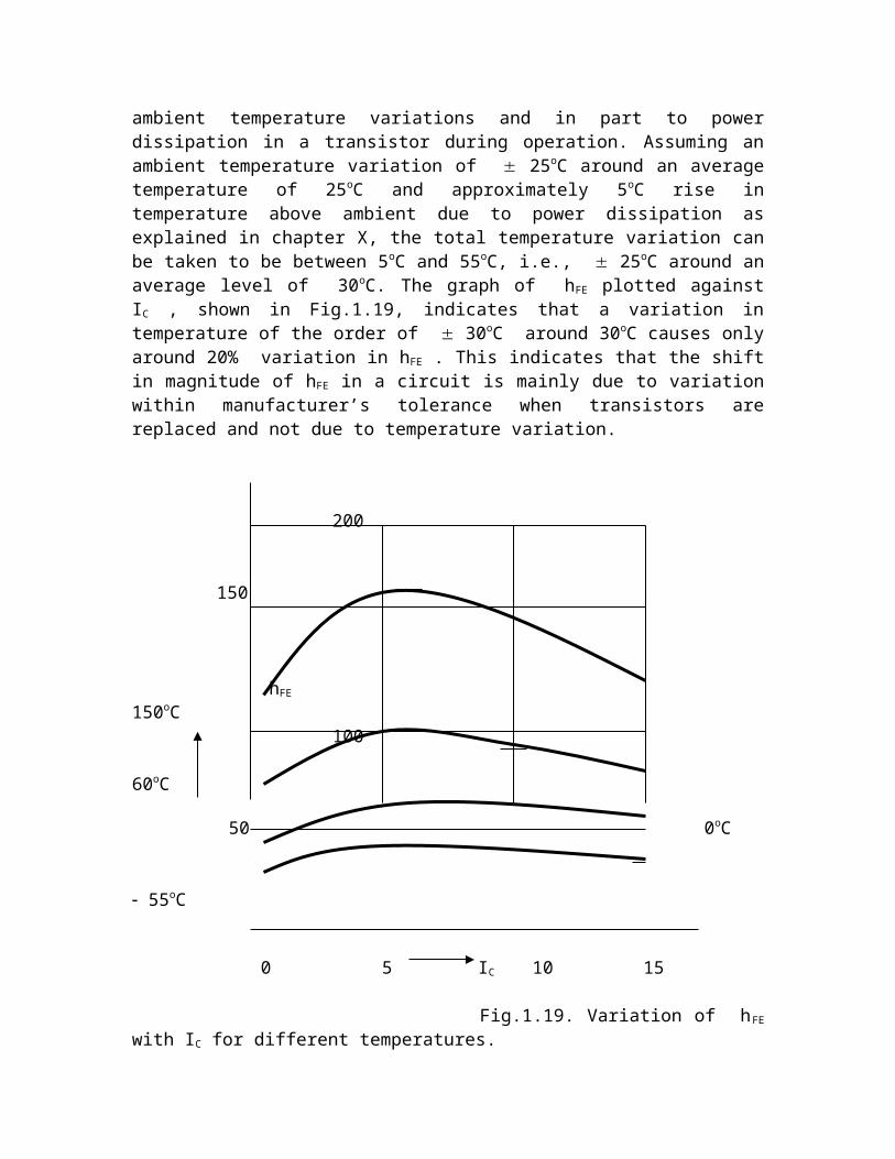
RS VDD
+ + + VGS + VS Vo
VS
(a) Connecting signal source to JFET (b) Connecting RD and VDD to obtain Vo
to obtain VGS proportional to VS Amplifies waveform with distortion
Fig.1.23. Building a JFET amplifier
47
A drain resistance RD and a dc supply VDD is connected as shown in Fig.1.23(b) to obtain output voltage Vo . which is, hopefully, proportional to VS . The relation between IDS and VGS being nonlinear according to eq.(1.27) linearity between Vo
and VS will be good only for small signal magnitudes as shown in Fig.1.24. This figure is drawn assuming IDSS = 10mA and VP = 8v. If an input signal, having a peak-to-peak amplitude of 2v, is applied between the gate and source terminals along with a bias voltage of 3v, the gate-to-source voltage will vary as shown by waveform A drawn below the VGS axis in the figure. Corresponding to this the output current will vary as shown by waveform A drawn to the right of the IDS axis. The output current is seen to be a reasonably good replica of the input waveform because the transfer characteristics within the operating range between P and M is reasonably straight. This is not true for the input and output waveforms shown as B in the figure, where the positive half of the output waveform has a larger amplitude than the negative half. This is because the transfer characteristics within the operating range between R and S is not a straight line. Smaller signal amplitudes will, obviously, exhibit better linearity between input and output.
R Manufacturer specifies IDSS and VP IDSS = 10mA
Transfer characteristics of JFET IDS
IDS = IDSS [ 1 (VGS VP)] 2
P
A B Q IDS0
VO VO
M Pinch off voltage VP = 8v

S Output signals VGS0
8v 6v 4v 2v 0 VGS
A
VIN
Input signals
B
VIN
Fig.1.24. Transfer characteristics of JFET showing effects of nonlinearity. 48
JFET amplifiers have high input impedance and because of this they are often used as input stages. In such applications they are expected to handle only small magnitudes of signal voltages and, therefore, the distortion components generated in the amplifier due to nonlinearities might be well within tolerable limits. Nonlinear distortion components produced can be reduced further, if necessary, by the application of negative feedback. There is, however, a major defect in the amplifier circuit shown in Fig.1.23(b) apart from nonlinear operation. The defect is that the circuit cannot amplify any signal without serious distortion. The reason for this can be understood from the waveforms, shown in Fig.1.25, pertaining to the circuit
VS
0 t
(a) Input signal voltage waveform
VGS
0
(b) Gate-to-source voltage waveform
Fig,1.25. Waveforms for the circuit shown in Fig.1.23(b)
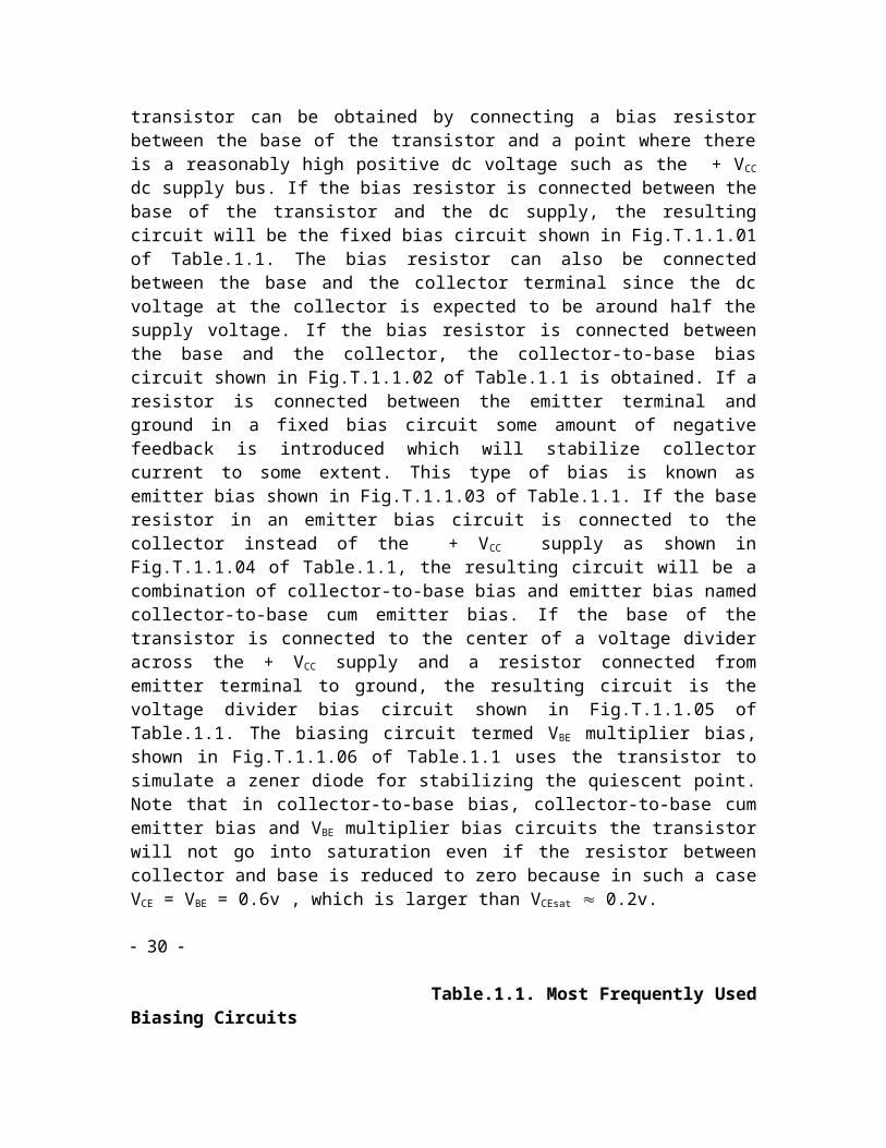
For the circuit shown in Fig.1.23(b) the signal is assumed to be a sine wave as shown in Fig.1.25(a). During positive half cycles of the signal waveform the polarity VS will be as shown in the figure and the current tends to flow in the clockwise direction in the gate loop. This is the forward direction for the gate-to-source junction and current will flow in the loop. There will be a voltage drop VRS across the resistance RS
and gate-to-source voltage will be VGS = ( VS VRS). Gate-to-source voltage will be less than VS and this is indicated by a low amplitude sine wave for positive half cycles in Fig.1.25(b). During negative half cycles of the signal waveform the polarity of VS will be such as to send a current in the anticlockwise direction in the gate loop. Since this is the reverse direction for the gate-to-source junction current will not flow. There will be no voltage drop across RS and gate-to-source voltage VGS will be equal to VS . This shows that the signal waveform gets distorted right at the input point of the amplifier and the output cannot be expected to be any better.
49
VGS
VGS0
0
(a)With forward bias equal to VGS0 VGS
0
VGS0
(b) With reverse bias equal to VGS0
Fig.1.26. Gate-to-source voltage waveform with bias applied.
The remedy for this problem of distortion at the input is similar to that suggested for the BJT circuit and that is to apply bias. Since JFET is a voltage controlled device a voltage bias is applied. For JFET circuits there are two options for biasing. One is to raise the complete VGS waveform above the time axis by applying a positive voltage bias VGS0 as shown in Fig.1.26(a) and the other is to lower the complete VGS waveform below the time axis by applying a negative voltage bias VGS0 as shown in Fig.1.26(b). For positive bias the gate-source junction will be conducting for the full cycle of the signal waveform, VGS will be much less than VS ,as shown in Fig.1.26(a), and power will be drawn from the signal source. For negative bias the gate-source junction will be reverse biased for the full cycle of the signal waveform with no current in
the gate loop, VGS will be equal to VS , as shown in Fig.1.26(b), and no power is drawn from the signal source. This shows that negative bias is the better of the two options available for biasing the n-channel JFET.
There are different ways of applying the negative bias required to the JFET. The most obvious method is to apply a negative voltage to the gate terminal with the source terminal grounded as shown in Fig.1.27. Fig.1.27(a) shows the bias applied in series with VS and Fig.1.27(b) shows the bias applied in parallel with VS . Since the bias battery VGG supplies a negative voltage with respect to ground, the drain supply + VDD which supplies a positive voltage with respect to ground cannot be utilised for biasing. This means that each stage of JFET circuit will require a separate battery for
50
+ VDD + VDD
RD RD
RS RS C
+ +RG
VS VS
VGG
RG VGG
(a) Bias applied in series with VS (b) Bias applied in parallel with VS
Fig.1.27. Two methods of applying negative bias to JFET circuits : both inconvenient.
biasing if bias is applied in series with VS or a single battery with connections to each stage if bias is applied in parallel with VS . Both methods are inconvenient since extra batteries are required for biasing.
A more convenient way of biasing without the need for extra batteries is shown in Fig.1.28. Assume that the JFET selected for use in the amplifier has transfer characteristics shown in Fig.1.24 with IDSS = 10mA and VP = 8 volts. If the quiescent point Q is chosen as shown in Fig.1.24, quiescent drain current IDS0 = 4mA and quiescent gate-to-source voltage VGS0 = 3 volts. If a resistance equal to 750 is + VDD
RD
IDS = 4mA RS C + + + VS VRG RG RSO = 750
3v
Fig.1.28. JFET amplifier with self bias
51
connected from the source terminal of the JFET to ground, the 4mA quiescent current passing through it will develop 3 volts across it, as shown in the figure. If the gate-to-ground voltage is negligibly small VGS = IDS RSO = 3 volts and the quiescent point will be located at the point chosen. With RG absent, the voltage between gate and ground is, by and large, indeterminate. RG is connected to fix the voltage between these two points. With RG connected the dc current through it will be the reverse saturation current ISG of the gate-channel junction which is usually around 10nA. If RG is restricted to 10M, VRG the voltage drop across it will be of the order of 100mV, which is negligible compared to the 3 volts across RSO so that VGS = VRG IDS RSO 3 volts as required. In JFET amplifiers the resistance RG is required and its value should be restricted to a maximum of around 10M to make VRG the voltage across it negligible compared to the bias voltage VGS0 developed across RSO . If this is not done the reverse saturation current ISG , which is temperature sensitive, will cause VRG and, consequently, the quiescent bias voltage to vary with temperature. This circuit is known as the ‘‘self bias’’ circuit because the current through the device itself is used for developing the voltage required for biasing.
DC analysis of the JFET self bias circuit
DC analysis of the self bias circuit is to find out the quiescent values of IDS and VGS . This can be done either (a) mathematically or (b) graphically.
(a) Mathematical analysis of JFET self bias circuit
The quiescent point or dc operating point (V GS0 , IDS0) must lie on the transfer characteristics of the device. This means that VGS0 and IDS0 must satisfy the equation for the transfer characteristics given by
……..(1.28)
It is seen from Fig.1.28 that the gate-to-source voltage VGS of the JFET is given by
VGS = VRG IDS RSO
Assuming that VRG is made negligible by choosing RG smaller than 10M
VGS IDS RSO ……..(1.29)
VGS0 and IDS0 must satisfy eq.(1.29) also. Substituting VGS0 for VGS and IDS0 for IDS in eqs.(1.28) and (1.29) and solving, the quiescent parameters VGS0 and IDS0 can be evaluated.
52
(b) Graphical analysis of the JFET self bias circuit
Transfer characteristics IDS = IDSS [ 1 (VGS VP)] 2
IDSS = 10mA
Bias line VGS = IDS RSO
Q IDS IDS0 = 4mA
Pinch off voltage VP = 8v VGS0 = 3v 8v 6v 4v 2v 0 VGS
Fig.1.29. Quiescent point as intersection of bias line and transfer characteristics
The first step in the graphical analysis of the JFET self bias circuit is to draw the transfer characteristics of the JFET defined by eq.1.28, as shown in Fig.1.29. The quiescent point lies on this curve. The quiescent point must also satisfy eq.(1.29) which represents a straight line known as the ‘‘bias line’’. The second step in the graphical analysis is to draw the bias line as shown in Fig.1.29. The point of intersection of transfer characteristics and bias line represents the quiescent point indicated as Q in the figure. The parameter I DSS of the JFET shows a manufacturer’s tolerance as wide as that of the hFE of the BJT. The manufacturer specifies IDSS in terms of a minimum value IDSSmin and a maximum value IDSSmax . The ratio IDSSmin : IDSSmax is usually around 1 : 3 . If IDSSmax is 10mA, IDSSmin will be around 3.3mA. The transfer characteristics corresponding to these two values of IDSS are as shown in Fig.1.30. The transfer characteristics for typical value of IDSS , i.e., IDSStyp = 6mA is also shown in the figure. It is seen that the quiescent current IDS0 is 4mA, 3.3mA and 1.2mA corresponding to IDSSmax , IDSStyp and IDSSmin respectively for the bias line shown. The quiescent current IDS0
can take any value between 4mA and 1.2mA due to IDSS variation within manufacturer’s
tolerance. If this order of variation for IDS0 cannot be tolerated different methods of biasing will have to be used.
53
Transfer characteristics IDS = IDSS [ 1 (VGS VP)] 2
IDSSmax = 10mA
IDS Bias line VGS = IDS RSO IDSStyp = 6mA
Q1 IDS0max = 4mA
Q2 IDSSmin = 3.3mA
2mA Q3 IDS0min = 1.2mA 8v 6v 4v 2v 0 VGS
Fig.1.30. Shift in quiescent point due to manufacturer’s tolerance in IDSS
Constant current bias for the JFET One way of stabilizing the drain current I DS is to connect a constant current generator, simulated by a voltage divider bias constant current circuit, to the source terminal as shown in Fig.1.31(a). This will hold IDS constant in spite of IDSS
variations, at I0 the value set by the voltage divider bias circuit. The quiescent points corresponding to IDS = I0 will be located at Q1 , Q and Q3 as shown in Fig.1.32 This method of stabilizing IDS requires an extra transistor and a few resistors. + VCC + VCC
R1
+
VGG = VCC R2 R2 RSO
R1 + R2
IDS
(a)Constant current bias (b) Voltage divider bias
Fig.1.31.Methods of stabilizing drain current in JFET amplifiers 54

Voltage divider bias for the JFET A simpler, less expensive though slightly less effective way of stabilising the drain current is the voltage divider bias shown in Fig.1.31(b). For this circuit the gate-source junction will be reverse biased and no current flows into the gate and, therefore, the voltage at the junction of R1 and R2 , designated VGG , is given by
VGG = ……..(1.30)
The gate-to-source voltage VGS of the JFET is given by
VGS = VGG IDS RSO ……..(1.31)
Eq.(1.31) is represented graphically as the bias line in Fig.1.32. The quiescent points corresponding to this bias line will be located at QA , Q and QB. Note that the location of the quiescent point lies between QA and QB . This variation is less than that seen in Fig.1.30 for the self bias circuit which means that voltage divider bias circuit gives better stability for IDS than self bias circuit. Obviously, larger values of VGG gives better stability of IDS in voltage divider bias circuit. This type of biasing is, therefore, suitable in cases where the supply voltage VCC is large so that VGG , derived from VCC , can be made large to obtain better stability for IDS . This will automatically mean a large voltage between source terminal and ground since VGS is likely to be around 1 to 4 volts only. This type of biasing is very much suitable for common drain amplifiers, i.e., source followers. IDSSmax
IDS
Bias line (Voltage divider bias) IDSStyp [ VGS = VGG IDS RSO ]
QA Q Q3 IDSSmin IDS = I0
Bias line (Constant current bias) QB VGG
8v 6v 4v 2v 0 VGS
Fig.1.32. Bias lines for constant current and voltage divider bias circuits
55
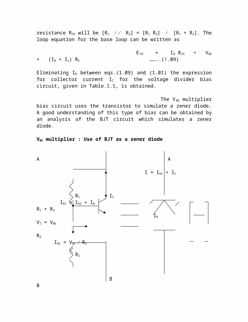
A logical way of designing the voltage divider bias circuit will be to locate the quiescent point Q on the typical characteristics and fix acceptable shifts QA
and QB on the maximum and minimum IDSS characteristics respectively. Joining QA and QB by a straight line and extending it to meet the VGS axis will determine the value of VGG
. The slope of this bias line will indicate the value of RSO . Eq.(1.31), the bias line equation, and the restriction that the current through R1 and R2 should be large compared to the reverse saturation current of the gate-channel junction of the JFET will fix R 1 and R2 . The reverse saturation current of the gate-channel junction being of the order of nanoamperes, this condition can be satisfied even if the resistances R1 and R2 are of the order of megohms. Amplifier constructed using FETs are, therefore, capable of providing high input resistance without any special circuitry.
MOSFETs MOSFETs are by far the most significant and widely used electronic device currently, especially in the design of integrated circuits. BJTs and MOSFETs offer unique features and areas of application. MOSFETs can be made very small on the IC chip compared to BJTs so that these devices can be packed more densely. The manufacturing process of MOSFETs is relatively simple. MOSFET circuits require comparatively little power for operation. Since resistors occupy large chip area substantial saving in chip area can be achieved by using MOSFETs connected as active loads in place of resistors. Use of active loads in place of resistors will also result in much higher voltage gain. MOSFET integrated circuits operating at 3 to 5 GHz are now quite common. Careful design, proper choice of material and physical structure have pushed the upper frequency limit of MOSFETs and its variations such as MESFETs and high electron mobility transistors (HEMTs) to several tens of GHz whereas for BJTs the upper frequency limit is only a few GHz at best. Ingenious methods have been found to implement analog and digital functions in the same IC chip utilizing MOSFETs almost exclusively with very few or no resistors in what is known as mixed signal design. All of these properties have made it possible to pack more than 200 million MOSFETs on a single IC chip to implement very sophisticated very large scale integrated (VLSI) circuits such as those for memories and microprocessors. These developments have paved the way for the design of powerful desktop computers, hand-held calculators, cell phones, etc. Although discrete MOS transistors exist, most of the applications of MOSFETs are in integrated circuit design. Even though JFETs were developed before MOSFETs, applications and uses of MOSFETs have far surpassed those of JFET.
56
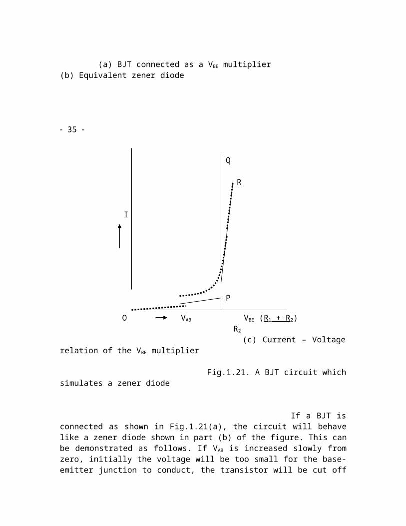
Biasing Circuits for MOSFETs
(i) Enhancement-mode MOSFET
Enhancement-mode MOSFETs are the most widely used field-effect transistor. The very popular CMOS family of digital circuits also uses enhancement-mode MOSFETs. Biasing circuits for n-channel enhancement-mode MOSFETs can be designed using the voltage-to-current transfer characteristics of the device shown in Fig.1.33 and defined by the equation
IDS = K ( VGS Vth )2 ……..(1.32)
where, Vth is the threshold voltage of the transistor and K a constant. Note that eq.(1.32) is valid for the region where VGS > Vth . The manufacturer specifies Vth and the value of IDSon corresponding to a specified value of VGSon . The constant K appearing in eq.(1.32) can be evaluated using this data. Expressing K in terms IDSon , VGSon and Vth , eq.(1.32) can be written as
……..(1.33)
Typical characteristics
Constant voltage bias line
IDSO1
IDSon
Constant current bias line IDS
IDSO2
A practical bias line (Voltage divider bias)
IDSO3
Vth VGSon
VGS
Fig.1.33. Transfer characteristics of the n-channel enhancement-mode MOSFET
57
The firm curve shown in Fig.1.33 represents a typical transfer characteristics of an n-channel enhancement-mode MOSFET. The dashed curves represent the limits of tolerance specified by the manufacturer for the transfer characteristics. A positive bias voltage VGS is required to locate the quiescent point at a suitable position on the transfer characteristics of the MOSFET. A positive bias voltage can be easily derived from the VDD supply voltage by using the circuit shown in Fig.1.34(a). The bias voltage VGSO for such a biasing circuit will be given by
VGG = VGSO = VDD ……..(1.34)
The bias voltage VGSO is a constant independent of the transistor used. Such an arrangement constitutes a constant voltage bias represented by a vertical bias line parallel to IDS axis as shown in Fig.1.33. For such an arrangement IDSO , the quiescent drain current varies very widely from IDSO1 to IDSO3 for the three characteristics shown for the same transistor. Such a biasing arrangement is to be avoided in the interest of a stable quiescent point.
+ VDD + VDD
R1 RD R1 RD
VGG VGG
R2
R2 RSO
(a) Constant voltage bias with poor (b) Voltage divider bias with acceptable stability for quiescent point stability of quiescent point
Fig.1.34. Biasing methods for n-channel enhancement-mode MOSFETs
58
An ideal solution for obtaining a very stable quiescent point will be to use a constant current circuit in an arrangement similar to that shown in Fig.1.31(a). This will result in a circuit shown in Fig.1.34(b) with RSO replaced by a constant current circuit using a BJT voltage divider bias circuit. This will require an extra transistor and
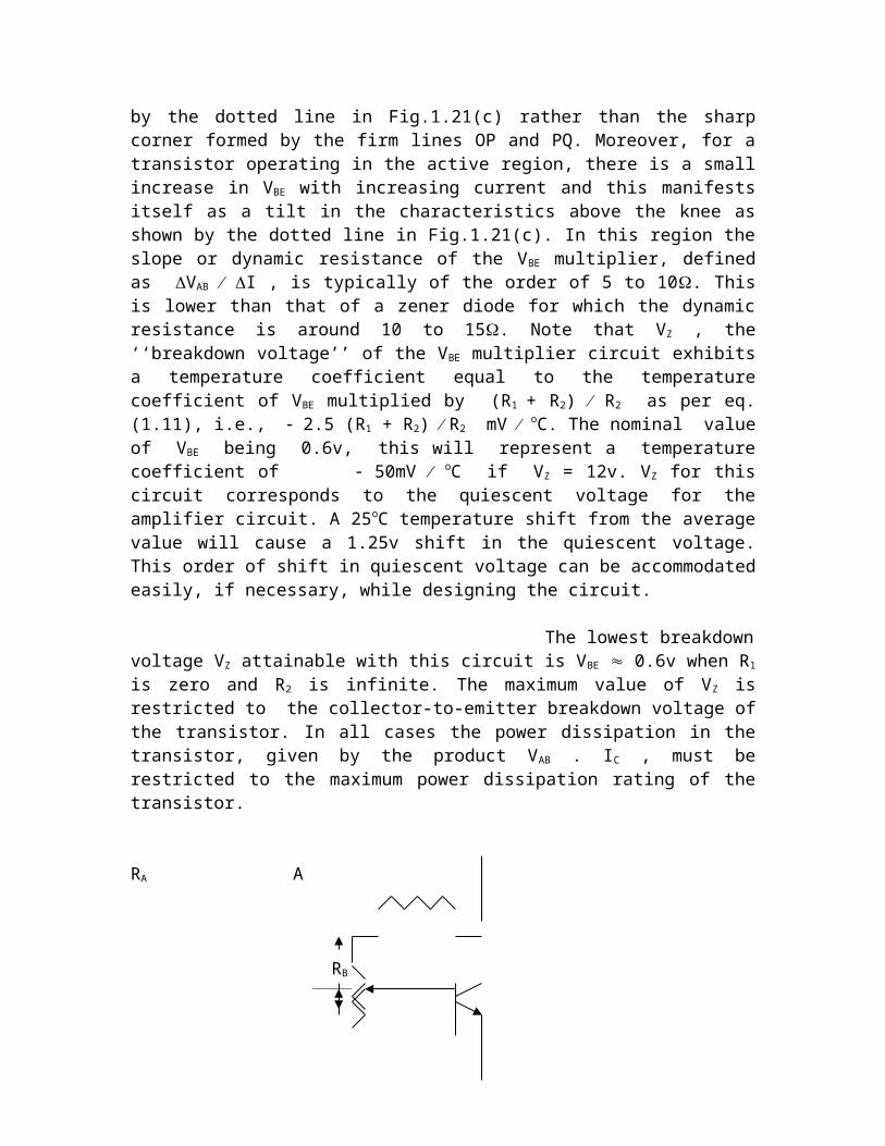
associated resistors. A more practical solution will be a voltage divider bias circuit shown in Fig1.34(b). The bias line for such an arrangement is shown in Fig.1.33. The design of voltage divider bias circuits for MOSFETs follows the same pattern discussed in connection with the design of voltage divider bias circuits for JFETs.
(ii) Depletion-mode MOSFET
Biasing circuits for n-channel depletion-mode MOSFETs can be designed using the voltage-to-current transfer characteristics of the device shown in Fig.1.35 and defined by the equation
IDS = IDSS ……..(1.35)
where, Vth is the threshold voltage of the transistor and IDSS the value of IDS when VGS is zero. Eq.(1.35) is valid for the region where VGS > Vth . The manufacturer specifies Vth
and IDSS for the transistor. Vth in this case can be thought of as the pinch-off voltage of the transistor similar to that of the JFET.
IDS
IDSS1
IDSS Bias line for
voltage divider bias
IDSS2
Vth VGS
Fig.1.35. Transfer characteristics of the n-channel depletion-mode MOSFET
59
The firm curve shown in Fig.1.35 represents a typical transfer characteristics of an n-channel depletion-mode MOSFET. The dashed curves represent the limits of tolerance specified by the manufacturer for the transfer characteristics. The gate current is zero for all MOSFETs because of the insulating silicon dioxide layer between the gate terminal and the channel. The device can, therefore, be operated successfully with positive or negative values of gate-to-source voltage VGS without any noticeable difference and no bias voltage is necessary for operating the depletion-mode
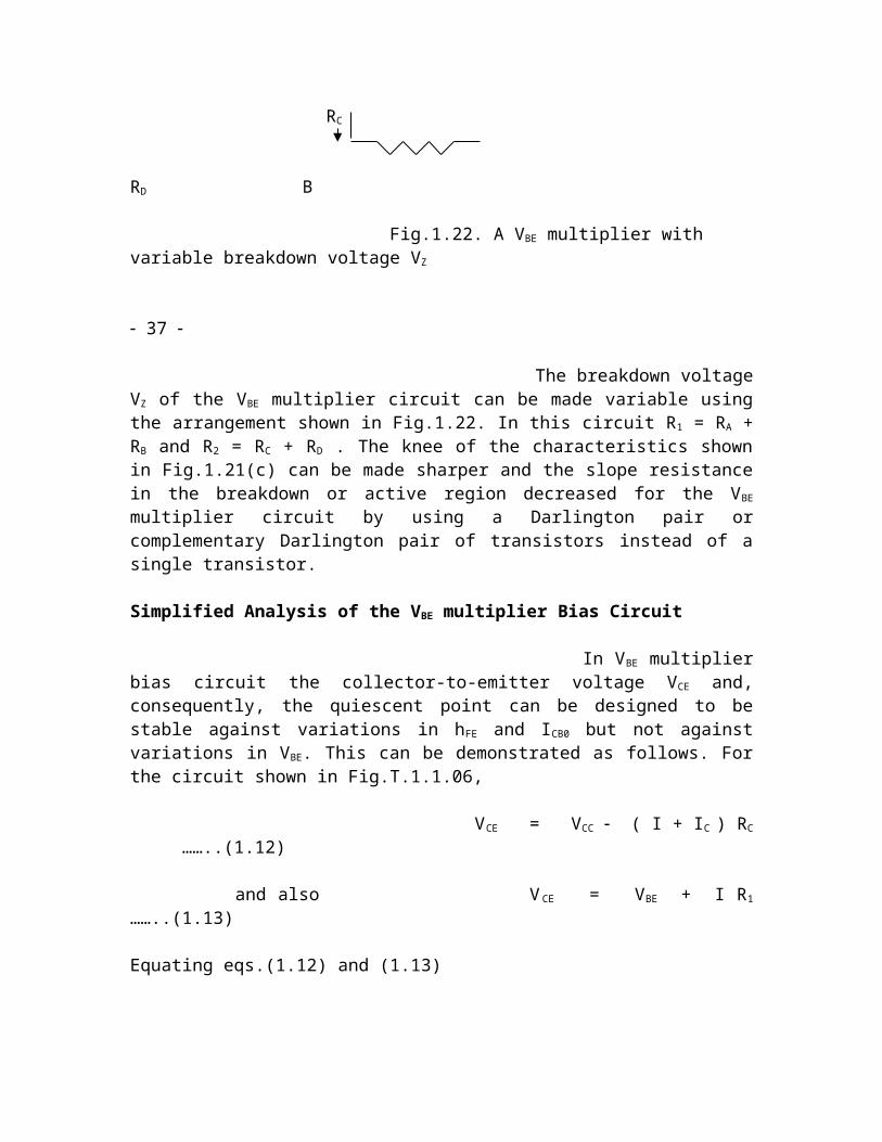
MOSFET. However, variation of transfer characteristics of the device within manufacturer’s tolerance causes the quiescent current to vary between IDSS1 and IDSS2 as shown in Fig.1.35 for zero bias. The ideal solution to this problem is to use a constant current bias in a circuit arrangement shown in Fig.1.36(a). A simpler solution which can overcome this problem to a large extent will be to use a voltage divider bias as shown in Fig.1.36(b). The bias line for the voltage divider bias circuit is indicated in Fig.1.35.
+ VDD + VDD
RD
R1 RD
R3 R1
R2
R2
RE R4 RSO
(a) Constant current bias (b) Voltage divider bias
Fig.1.36. Biasing methods for n-channel depletion-mode MOSFETs
60
Circuit techniques particularly useful in integrated circuits
Current Mirrors
Current mirrors are basically constant current circuits which can be implemented very easily in integrated circuits. The operating principle of this circuit is based on the fact that all the transistors manufactured to the same dimensional specifications in a given IC chip will have identical electrical characteristics.
(a) Current mirror using BJTs
+ VCC + VCC

R
IC1 IC2 ICn Iref IC1 Iref
ICref Q1 Q2 Qn
IB1
Qref Q1 Qref
IBref
(a) Two-transistor (b) Multi-transistor
Fig.1.37. BJT current mirrors
The BJT two-transistor current mirror shown in Fig.1.37(a) is the basic building block for the design of constant current circuits in ICs. For this circuit
Iref = = = ICref + IBref + IB1 ……..
(1.36)
The two transistors in Fig.1.37(a) have the same base-emitter voltage. Assuming Qref and Q1 to have identical characteristics because they are on the same IC chip and because they have the same base-emitter voltage, ICref = IC1 and IBref = IB1. Substituting these values in eq.(1.36),
61
Iref = = IC1 + IB1 + IB1 = IC1 + 2 = IC1 ……(1.37)
Or
IC1 = = ……..
(1.38)
Note that IC1 given by eq.(1.38) is a constant current with the collector voltage of Q1 free to swing with the signal. Using the same approach it can be easily shown that for the multi-transistor circuit shown in Fig.1.37(b)
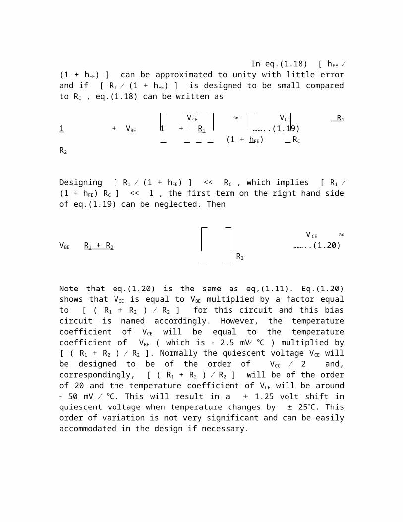
IC1 = IC2 = …….= ICn = = ……..
(1.39)
Eq.(1.39) shows that each of the transistors Q1 to Qn behaves like a constant current device and can be used at a different place in an IC.
(b) Current mirror using MOSFETs


![f arXiv:1704.00876v1 [cond-mat.other] 4 Apr 2017 · Analysis and validation of low-frequency noise reduction in MOSFET circuits using variable duty cycle switched biasing Kapil Jainwal,](https://img.pdfslide.net/doc/110x75/5f1760ce3cd697494a47b9f8/f-arxiv170400876v1-cond-matother-4-apr-2017-analysis-and-validation-of-low-frequency.jpg)