Embed Size (px)
Citation preview

1
Chapter 1
Brief introduction
1.1. Brief introduction
It has become the requirements of storage devices, because the computer era drawing. In
particular, this memory should be associative in nature. For practical purposes, this memory
also need fast and cheap. Most storage device stores and by addressing specific memory
location to retrieve the data. As a result, this path has become dependent on access to the
system flash memory constraints. To find that time is stored in a memory in the project
needed can be significantly decreased if the project can access its content by replacing its
address is recognized. Can be accessed in this way is called content-addressable memory
memory (CAM). Thus, content addressable memory (CAM) is one such memory is fast and
intuitive.
CAM's action coincided with the rapid increase in the cost of power and area. CAM fast
operation due to the content of all the contents stored in the memory of the parallel search
operations in a single clock cycle. That is, CAM simultaneously retrieves content stored in
the memory of all input words. However, this would result in high power dissipation of the
CAM. The large number of adhesion molecules needed to compare the operation will
consume a lot of power. Therefore, since the comparison operation and a large number of
parallel CAM search operation, the power consumption is always a problem CAM design of
major concern.
Unlike conventional memory (e.g., RAM), in addition to the memory circuit, CAM has an
additional circuit for storing and retrieving data so that the data are compared. Therefore, no
more than in CAM RAM, but high speed due to the parallel search operations more power. In
addition, CAM circuit caused by such additional storage memory than normal physical size.
This makes the high cost is the major drawback of CAM CAM. Therefore, it is only used for
applications that require high-speed operations. There are various types of applications,
including high speed of operation is required. Adhesion molecules can be used in these types
of applications. However, the main application CAM is that it is used in high-speed network

2
router forwarding. Since the growth of CAM applications, there is a great problem CAM size
and power requirements of deterioration. Therefore, the main challenge is to reduce the
power consumption in large capacity CAM, without sacrificing its speed.
Therefore, we propose to use in which parity bits, and reduce the amount of architecture in
the CAM CAM comparison operations. Therefore, the proposed CAM architecture consumes
less power for, and to improve the search speed than the base of the CAM.
Table 1.1. CAM V / S RAM
CAM RAM
1. Hardware search engine intensive
applications.
2, CAM is a general guide SRAM and
additional comparison circuit.
3. Enter the address of the output data word.
The depth of the memory can be extended as
desired, but the width of the limited physical
size.
5. Mainly used for high-speed network
routers, and caching.
1. Physical memory to store data.
2. It may be SRAM, DRAM, etc., but no
additional circuitry.
3. Enter the production as output data word
address.
The depth is limited, the width can be
extended as desired.
5. for temporary storage.
1.2. Content Addressable Memory
Content-addressable memory (CAM) is one in which it can use its contents, instead of using
the accessed memory cell storage memory [6]. When the CAM receives input data word to
search it for the table stored in the CAM memory data word, it returns the data in which the
search word is stored in the address. The entire operation is done using active parallel circuit
in a single clock cycle [6]. Therefore, it is very fast, only in need of high-speed applications.
However, this will consume a lot of power.

3
A CAM word size is usually larger, i.e., the number of bits to achieve the range of the
conventional 36 to 144 [6] from. A typical use of the CAM table size range from hundreds to
32K entries. Corresponding address space in the range of 7-15 [6].
1.2.1. Basics of CAM cell
A content addressable memory to store data like a normal memory cell of a storage device for
storing. But in addition it also has its data contents for searching simultaneously with data
stored in its memory a comparator for comparing circuit. Thus, a basic CAM unit has two
functions [1]:
1. A memory storage as usual RAM. Therefore, this bit is stored using, which includes two
cross-coupled inverters form a positive feedback to work as D- latches simple SRAM cell.
2. Compare this corresponds bit XNOR logic operation. It means that the storage and search
bit are the same and different, when matched and mismatched situation. This bit Compare
function is unique in CAM.
Therefore, our primary structure of a CAM battery is designed to SRAM circuit that is D-
latches and an exclusive NOR circuit [1] of the vector product. Therefore, it has three
operating modes: read, write, and compare.
Due to the extra comparator circuit CAM, its physical size increases. This leads to the loss of
most of the silicon area which increases the cost of CAM. This is a major drawback of the
CAM.

4
Figure 1.1. CAM cell circuit unit [1]
Figure 1.1. It illustrates a circuit of a CAM cell. The following is a basic CAM unit, the
signal which is responsible for the basic operation of the CAM:
1. Enter the search data is that it is from the word register is entered in the CAM array or the
value is to compare the value of one bit of the signal coming from the value stored in the
CAM unit for all storage.
2. Cell is enabled to allow or block signal comparing namely matching process. If the cell
enable signal is "1", that is a logic high, then there will be between (XNOR operation) bits
and outputs a comparison process input bits and the stored data will indicate whether the
input matching and memory or do not match. If the cell is enabled is "0", that is not a logic
low bit-bit input and stored there, so any comparison between the power saving.
3. Write enable is a signal used in a cell for a write operation. If the write enable "1" to a
logic high, then the input bit is in the search data register is written to the cell.
The output indicates whether the input data matches with the stored data or the comparison
signal does not match. If it is "1", i.e., a high logic level of the matching data exists, if it is
"0", i.e., a logic low if there is a mismatch.

5
1.2.2. CAM word
Figure 1.2. The basic circuit configuration of a CAM word
Figure 1.2. The basic circuit configuration shown in CAM word. It shows a CAM CAM word
by the number of units. Each CAM cell has its own search line (SL). Its corresponding search
bit compared bits stored armor CAM unit disposed in a search line (SL). Similarly, all of the
word CAM unit simultaneously for comparison. All units share a CAM match line in the
word. Therefore, match line (ML) combination of a CAM word on the search results
generated. To match line ML is connected to the sense amplifier (MLSA), which senses the
state of the ML and tell whether the word match or mismatch of search data.
1.2.3. CAM type
They have based their bit storage capacity of the two types of CAM:
1. The two yuan CAM or B-CAM unit to store and search the binary value is '0' or '1', that is
either a logic high or logic low. Thus, CAM B is only suitable for applications that require
exact match search application.

6
2. The three yuan CAM or T-CAM cell further storage and search of "X", ie not care bit or
mask bits. This represents both irrelevant bits "0" and "1." Therefore, TCAM cells store and
search triples the value "0", "1" and "X" bits, thereby increasing the flexibility in data search,
but the extra cost of the CAM from more than B-.
T- of CAM: they are more powerful and feature-rich than the B- cam. Country "X" can be
used as part of the match to perform a wild card entry. Masking can be done both globally
that the search key, and that the stored entries in the table locally. Figure 1.3. It shows the T-
shaped masking CAM global and local examples.
Figure 1.3. (A), the search key 10110XXX will match all fall within the scope of the entry in
1,011,000,010,110,111 to (ie at address 1 and 4. In this case, the word). This is the last three
so-called global block all entries are ignored or do not care.
In Figure 1.3 (b), the word 110-XX-010 (at address 2) will match any of the following search
keys: 110-00-010,110-01-010,110-10-010 and 110-11-010. Masking feature is particularly
suitable for Classless Inter-Domain Routing (CIDR) longest prefix match search. T type of
CAM has become in solving other problems, such as sorting and searching pandemic.
Figure 1.3. T-CAM with (a) Global masking, and (b) local shelter.
1.2.4. CAM Applications

7
Some applications CAM are as follows:
• Network Routers
• In the network packet forwarding industry
• Compare the cache tags
• Data compression and radar signal tracking
• Virus detection and intrusion detection systems
• Real-time pattern matching
• gene pattern search in Bioinformatics
• Ultra-high-speed data transmission
• Translation Lookaside Buffer (TLB) Microprocessor
• I.P. Filters
• ATM Switch
But the main main application is in high-speed network routers forward packets.
Network routers forward packets Find feature from an input port of the outbound port, using
the address: packet forwarding using CAM applications. The address lookup function to
check the packet destination address and select the address associated with the output port.
Router maintains a list called contains the destination address and its corresponding routing
table output port. A simplified example of a routing table is shown in Table 1.3. Table all
four five words, irrespective of position, "X", these two matches a "0" and in the "1." Because
of the "X" position, the range of the first three entries in the table represent the input address,
that is a map of all inbound address range 10100-10111 port A. router searches the table for
each destination address of the incoming packet and select the appropriate output port. For
example, if a router receives a packet with the destination address 10100, the packet is
forwarded to the port A. In the case of the incoming address 01101, address the query while

8
matching entries in item 2 and Table 3. Entry 2 is selected because it has the least "X" in the
position, or, alternatively, it has the longest prefix, which indicates that it is the most direct
route to the destination. The query method is called longest prefix match.
Figure 1.4. It shows how CAM by implementing the routing table to complete the address
lookup. On the left side of Figure 1.4, the packet destination address of 01101 is input to the
CAM. As the table, two positions match with the (priority) of the encoder selects the top 01
entries and a match position, which corresponds to the most direct route. This location is the
input list to match the output port address to the included RAM as shown in Figure 1.4. A
RAM read output port identification, B port of the incoming packet is forwarded to. We can
see the position of the output of the CAM match as a pointer to retrieve words from RAM. In
the packet forwarding specific cases related words specify the output port. This CAM / RAM
system is a complete implementation of address lookup packet forwarding engine.
Figure 1.4. CAM use routing tables to achieve.
1.2.5. CAM design
CAM conceptual diagram is shown in Figure 1.5. It shows that the data contained therein
CAM store m data words. Search term for the n-bit input data. The input data is the data to be
searched in the memory. The n-bit data is broadcast to the search line while the comparison
with the stored word list. There are words associated with the matching line for each store.
This match line indicates whether the search data matches the stored data or not. If the search

9
data matches the stored data, it is the case of a match or not match the situation. The match
line is supplied to the encoder. This encoder generates corresponding match line indicates the
matching cases, the binary position. If more than one match line indicates the matching case,
then the priority encoder may be used to generate matching memory location. Priority
encoder provides the equivalent of the highest priority match line matches the address
position.
Figure 1.5. CAM conceptual diagram.
1.3. Match line (ML) segmentation techniques to achieve low power consumption
So far, more or all of the bits of the search process in the CAM words simultaneously or
uniformly executed, and they share the same ML. This heat is generated in each cell. Due to
this, there is a large amount of power consumption in CAM match lines. Therefore, it can be
said that the most power in a CAM waste is due to the matching lines. In almost the same line
of a CAM match each amount of energy consumed if there is a match or mismatch,
regardless of the particular data pattern. The ML power consumption can be greatly reduced
by dividing the match line of CAM i.e. word. There are two of the most popular match line

10
(ML) segmentation: One is selective precharge technique, and the other is a cell line
segmentation technique, an expansion selective precharge technique. Because of these
technologies, there is non-uniform distribution of power to match lines.
1.3.1. Select the pre-charging technology
Selective precharge technique, match line (CAM word) is divided into two segments, namely
the pre-search and main - search. First, a first section in which a small portion of the first few
bits of one word, i.e. CAM cells are searched in the search operation. If you just search the
remaining bits in the first data segment in matching the second section it will be activated.
Because if the first few do not match, then the corresponding CAM word will not match.
Therefore, the search in the second section of the remaining bits of no significance.
Figure 1.6. Line Break game :( i) conventional CAM, (B) Select the pre-charging.

11
If the technology initially before searching k bits, k bits after it matches a search for the
remaining bit CAM word. Uniform random distribution of data, which must search line only
(1/2) K that is CAM words in the second section. Therefore, to save energy. K is large
enough so that there is a mismatch in most words.
As an example, if you have a 144 word and selective precharge technique initially before
searching k = 3 bits, and the remaining 141 will only search for the word, and its former three
matches to complete. Having a uniform distribution of random data, this initial search should
only be allowed to (1/2) 3, which saves about 88% of the match line power [IEEE] line of the
second paragraph.
Cons: There are two possible elimination of overhead power:
1. To maintain speed, the initial matching execution, that is, before a few bits per bit can
draw more power than the remaining bits of the search operation.
2. Match the first few bits may be the same all the words in the CAM. This eliminates any
power saving. This is the worst case of this technology.
Perhaps, this is the most common technique, in order to save on power to match the line as
part of its implementation is simple and can reduce most of the power in many CAM
applications.
1.3.2. Pipelining
Selective precharge technique, CAM words are divided into two segments. It can be further
divided into a plurality of segments. In one CAM word is divided into a plurality of segments
of the technique known as pipelining. It is an extension of the selective pre-charging
technology.
In this technique, an assessment of each segment in a pipelined manner. In the first paragraph
of the match and only then when the next segment of the search operation will be activated,
and so on. If there is no match, then the match in any segment corresponding match line
operations suspended by the next stage of the closing thereafter. This leads to energy saving.

12
In this manner, the best match of power lines can be reduced. Figure 1.7. (A) in. Shows a
non-pipelined ml and 144 cells Figure 1.7. (B) in. ML reducing power lines, which matches
the 144 cell line is divided into four sections, each of which in turn contains the evaluation of
36 cells.
Figure 1.7. (A) Non-pipeline stage, (ii) pipeline stage is divided into four segments.
Figure 1.8. It shows an example contains five sections of the search operation match line
activities. The dotted line indicates the corresponding section (stage) in the power saving of
the entire match line mismatch, therefore. The main advantage of this technique is that it has
the same effect selective precharge technique.

13
Figure 1.8. One example shows a search operation ML activities.
Matching lines can be segmented such that each segment contains a single bit or CAM unit.
This method is called a cell dividing line technology, as shown in Figure 1.9. Thus, the pre-
charge basis to select bits and pieces of technology in operation. If the match in one cell of
only subsequent cell will be activated for the search operation. Otherwise, the matching
process will be aborted corresponding word. If there is no match, in any cell it is not
necessary for the operation of the word in any comparison further. Therefore, subsequent cell
is not activated.
Figure 1.9. A unit split pipelining.

14
Disadvantages: additional circuitry that is flip flops are required in each segment to activate
the operating result before segment match. So, there is some overhead power and area
overhead due to the addition to the trigger. There is also increased due to the pipeline stage
delay.
1.4. Thesis organization
The thesis is structured as follows:
Chapter 1: This chapter describes the introduction of CAM (content addressable memory),
and describes some of the basics of CAM.
Chapter 2: This chapter describes the various documents in this thesis work.
Chapter 3: This chapter describes the design concept and the various existing CAM
architecture work, low power consumption and high performance.
Chapter 4: This chapter describes the recommended work, which explains the concept behind
the proposed design, the basic design of low-power and high-performance CAM structure.
Chapter 5: This chapter describes the implementation and simulation results suggest that the
design of CAM, the results compared with the conventional CAM architecture.
Chapter 6: Conclusions and future scope of work described in this chapter.

15
Chapter 2
literature review
2.1.1. In [5], a new method is called block XOR PBCAM way to improve the low-power pre-
calculated based CAM (PB-CAM) [8] proposed efficiency. In this paper, we propose an XOR
block parameter extractor for low power PB-CAM. This paper presents the theory and
practice of proof to verify that the proposed block XOR PB-CAM can effectively reduce the
number of comparison operations compare the second part of the process to achieve greater
power reduction. This means that this method is more flexible and adaptive to the general
design. In addition, the proposed block XOR PB-CAM-bit parallel parameter may be
calculated only three XOR gate delay of any input bit length (constant delay search
operation).
2.1.2. In [6], an investigation is the latest development in a large-capacity content addressable
memory (CAM) design is completed. In this article, CAM and CAM first basics of traditional
architecture review. Then the network router packet forwarding CAM applications also
examined. In this article, we have discussed CAM design technology, construction at the
circuit level and reduce the level of power of the traditional CAM. In the circuit, we have
reviewed to reduce match-line power, including selective precharge and pipeline technology
matching line segmentation. At the architectural level, we have examined the reduction CAM
architecture bank that is counting method includes a selection of pre-computed CAM
structure and power consumption.
2.1.3. In [7], we propose a technique to reduce the content addressable memory (cam)
technique called pipelining match line power consumption. In this technique, the search
operation is performed by matching lines into paragraphs pipeline sabotage. Since most of the
stored word do not match on their first portion, then the subsequent search operation is
aborted segment. Accordingly, the power will be reduced. Saving pipeline ML is the result of
the activation of only a small segment matching portion.
2.1.4. In [8] proposed an architecture with low power consumption, low cost, low voltage,
previously called complete parallel computing based content addressable memory (PB-

16
CAM), and high reliability. This design is based on a pre-computed skill, to save power
consumption of the CAM reduction in the second part of the comparison process of
comparing the number of passed. In this design, a person counting method used to calculate
in advance. For this, one count parameter extractor is to use a chain full adder design, but it
increases the data bit length increases the delay.
2.1.5. [9] proposes a method to reduce the power consumption of the technology available in
the content-addressable memory (cam) match line, called the selective precharge technique.
With strict literature investigation, it was decided to modify the architecture and design CAM
to achieve low power consumption and high speed operation by reducing the comparison of
the number of the conventional CAM. To achieve this goal, we use an extra bit in each data
word stored in the data store. This extra bit is used as parity bits corresponding to the stored
data word. In the existing architecture of CAM, parallel to compare the contents of functions
in a single clock cycle for each CAM word (cell). Therefore, this design has to run fast, but
there are a lot of power consumption. To reduce this power consumption, there are two
techniques in one word for modifying the structure of the level comparison circuit. Although
these techniques to save power, but will increase its latency and area. Therefore, in the pre-
construction level calculation method it is proposed to reduce the number of comparators to
save electricity. A method is a method of extracting a person's number of parameters, and the
other is a block XOR method. However, these methods take a lot of area for storing bits of
these parameters and their extraction. They must also extract and search operation parameters
via the parameter memory, although it reduces the power consumption data comparison of
power loss. Thus, based on this approach, we have decided to adopt a parity bit as arguments
than previous PB-CAM it just a bit storage parameters, and reduce the number of comparison
operations to reduce power consumption and improve the ratio of performance to achieve
PB-CAM Traditional CAM.

17
Chapter --3
CAM ARCHITECTURES
3.1. Conventional cam architecture
Figure 3-1. Conventional CAM architecture.
Figure 3-1. Size shows the size of the four included three data word conventional CAM
architecture of a 4x3. Each row horizontally, where each row represents containing 3 (CAM
unit) stored data word. There corresponds to each bit of the search word and ML
corresponding to each store a word entered MLSAs on SL. In the search operation starts: the
input data to be searched is given as input in the CAM and loaded into the search data
register. The input data broadcast by the search register their corresponding bits of data on
each SL. The parallel comparison of the data of each memory cell, wherein each CAM unit

18
compares its stored bits, carried out in the corresponding bit in SL. ML containing matching
data will be at a logic high or else from a logic low. The MLSAs, then the measurement data
matching state sense of the word, that is, whether or not the data word matches the data word
containing the matching state induction ML or mismatched data under. Then, according to
state data word match, the encoder will generate, it matches, the input data, in which data is
to be found in search data word address location.
3.2. Pre-computation based CAM (PBCAM)
So far, we have discussed the circuit-level technology, namely in the first chapter of the game
line segment CAM circuit technology to reduce power consumption. Even with these circuit-
level technological innovation, a general CAM array (word) exhibits a very high power
consumption compared to RAM, and if it is directly used to build large-capacity CAM.
Therefore, the study has been initiated to reduce power consumption level architecture.
CAM architecture in general, that the input data into the data search data stored in CAM and
all the while the CAM in comparison. Thus, CAM perform a number of comparison
operations during a search operation for each search data stored in the CAM. From these
comparison operation, most of the total power is consumed CAM. In order to minimize the
power consumption during the compare operation, one of the best ways is to reduce most of
the comparisons. Based on this idea, in the development of CAM architecture called
PBCAM.
3.2.1. design concept
For reducing power CAM architecture level technical structure is called pre-calculated, based
on the overall architecture is called content-addressable memory pre-computed. This method
is similar to selective pre-charging technology. In the pre-calculated, and each data word
CAM some extra information is stored, so that power is maintained. Thus, the search data
comparison operation is divided into two portions, i.e., pre-calculating unit (parameter
comparison unit) and the data comparison section. Along which is then stored in the

19
appropriate words from their own use of a special pre-calculated circuit in extra bits derived.
These bits before the main word data search section is used to compare pre-calculation
section, for the initial search. If the initial search does not match, then the CAM aborted then
that looking main character (in the data comparison section) search. Therefore, there is a
saving of power, but it also has some disadvantages, i.e., require additional hardware, thereby
increasing the area.
PBCAM conceptual diagram is shown in Figure 3.2. The concept of this architecture is to
increase and use an additional hardware, namely parameters extracted. Therefore, PBCAM
architecture parameters extracted from, parameter memory and data memory. That is
compared to the data memory ķ << n The parameter memory is very small.
Figure 3.2. PBCAM conceptual diagram.
Write operation in the data, with data to be written in the CAM is given as an input in CAM.
Parameter extractor extracts the parameter data of the input data input, which parameters are
then stored in the respective data memories and parameter memory.

20
In the data search operation, comparison operation is divided into two parts, in order to
reduce the large number of comparisons. The first part is a part or portion of pre-calculated
parameters more. Process is also known as pre-calculated parameter comparison process. In
the first section, enter the data parameters calculated in advance all the corresponding word
memory circuit called a parameter extractor extracted, and then the parameters of the input
data stored in the data memory of the parameter memory of the parameters by comparing
parameters comparator circuit in parallel. If the input data does not match the stored
parameters and parameter extraction, then at the same time on the input data is mismatched
data corresponding parameters stored do not match the stored. If the parameter is matched,
the corresponding processing from the first comparison matches the stored parameters
DATAS having stored in said second comparison process to compare. Based on these two
comparison process, if the majority of the stored parameters do not match the parameters of
the input data, and then comparing the number of the second comparison processing is highly
reduced, thereby saving power in the CAM. This parameter comparison process is to filter
most of the stored data does not match the input data, and to reduce the most comparison
operations in the second comparison processing. Therefore, we can say, function parameters
comparison process is the same filter.
In this PB-CAM architecture, most part relatively power by the parameter extractor mainly
due to the number of the circuit judges data, its argument is the same as the input, and the
input can be compared after processing and parameters Data match (pre-calculated). In
addition, both the parameter memory and architecture PB-CAM parameter comparison circuit
(parameter extractor) requires additional hardware cost and power consumption compared to
conventional CAM architecture. Therefore, the design parameter extraction is possible and as
much as possible of the shortest bit length of the filter as much data as possible and determine
unmatched (decrease) in comparison operations in the second part of the parameters of the
comparison required number. Therefore, the parameter extractor PBCAM plays a significant
role.
Some methods have been proposed, namely parameter extractor has achieved a PB-CAM
architecture parameter extraction, such as those calculation methods and Block-XOR method.

21
3.2.2. A one’s counting method
In this method, the input data of a person to be searched number is taken as the parameter for
reducing the large number of CAM compare operation. A person enter these numbers to
extract data from the use of a special circuit. Thus, in this method, a circuit (parameter
extractor) is designed for this purpose is called counter parameter extractor 1. When the data
to be searched is given as input in a CAM Then, the parameter extractor (PE) of this type in
the input data count (extraction) number of. Thus, the role of a person's count parameter
extractor like a counter.
It assumes that the input data is n bits in length, then a count of the number of the n + 1 (n
and 0 to one of). In addition, the need to express an additional type of counting a count to
indicate the availability of additional state data stored. Therefore, the minimum length
required bit parameter equal to k = [LOG2 (n + 2)].
Shows a man counting method example is given in Figure 3.3. There is a memory in which
data words are stored in the table. Together with the data word, a man of their respective
count is also stored in the table to the left of the table stored in the data word. In this example,
enter the word count one "0000101" is "2", which is the first time in the left table all stored
parameters were compared. Only the second and a fourth data word count is matched to only
its own number "2." So now only the second and fourth data word in parallel with the input
and the input data were found that matched the fourth word line ML3 word "0000101"
(matching) phase comparison. Thus, corresponding to the character ML3 address location
will be output.

22
Figure 3.3. An example of one’s counting methods.
Said one of the count parameter is used to extract a lot of full adder (FAS) implementation.
Figure 3.4. It shows a block diagram of the implementation of sports in people counting
methods. If the data is n bits, the circle element uses [N / 3] of the FA, to generate a partial
sum of n bit parallel input data. The output of these [N / 3] the FA is [N / 3] the sum signal
and [N / 3] to carry signals. Now, at the same time, located in [n / 3]-bearing signals to the
left link and [N / 3], and to the right link signal element comprising on a circle and the like.
According to this definition, the one of the count parameter extractor circuit is designed as
shown in Figure 3.5. This parameter extractor is designed with an example of 14-bit data.
Thus, the need for storing parameters i.e., a count in the memory is equal to the bit length
parameter k = LOG2 (14 + 2) = 4 bits.
Disadvantages:
1. Since a person's count parameter extraction is achieved using a number of FA, it has a very
complex calculation scheme, it also consumes huge power and hardware, which is not only a
waste of space, but also increase the delay.
2. loss of silicon region reserved for storing precomputed bit.

23
3. The median increase in the number of words, PE of this type of delay will significantly
increase. Also the count increases, which further increases the count of the number of bits
required to store the memory.
Figure 3.4. Count parameter extraction block diagram of one count.

24
Figure 3.5. 14 the number of people extraction circuit design.
3.2.3 block XOR method
In order to overcome the area overhead and power consumption count parameter extractor
disadvantage of a person, the block XOR method are introduced.
In this method, the input data bits are first divided into several blocks. It is used to calculate
the exclusive OR logic operation from each of these blocks, the output bits. Each output bit is
just a parameter bit data word parameters. Each block is given a parameter bit. These
parameter bits are combined to form a parameter, to reduce the number of comparison
operations in the second portion of the comparison process. Thus, in this method the
parameter to the parameter for the XOR data word block design is called extraction. Figure
3.6. XOR parameter extractor block design shown is n bits.
If the length of the input data is n bits, the parameters of length k = [LOG2 paragraph (n + 2)]
is counting method in a person. Thus, the input data blocks in which the number of bits in this
manner is given by dividing the n / LOG2 section (n + 2). An example of input data length 14
taking the length parameter is LOG2 (14 + 2) = 4 bits. Thus, in this method the number of
partitions of block [14 / LOG2 (14 + 2)] = 4. Thus, all blocks containing 4, except the last,
which contains only the remaining portion of the upper half 2 shown in Figure 3.7. [5].
Figure 3.6. XOR parameter n-bit block extraction [5].

25
However, the concept of block XOR method is not used to check whether the data is valid or
invalid, and therefore it can not be applied directly to PBCAM provide a valid bit. That is
why, in the lower part of the architecture is amended as shown in Figure 3.7. A valid bit. The
multiplexer is applied to select the correct parameters. The selected signal is defined as
S = A3A2A1A0. (1)
According to (1), if the parameter is from "0000" to "1110" (S = 0), the multiplexer sends
data I0 as an output that is the parameter does not change. Otherwise, (A3A2A1A0 = '' 1111
", S = '1'), i1 data multiplexer will be sent as the first block output and input data into a new
parameter, and" 1111 "can be used as effective bits. Note that, where the first block is "1111"
is not considered, because "1111" bit blocks, would result in the bit "0" of the four
parameters [5] of One.
Figure 3.7.
Thus, the block XOR parameter extractor can be calculated in parallel parameter bit only
three XOR gate delay of any input bit length, the search operation, so constant delay. And in

26
a person's counting method, a number of people with the input of the digital PE increased
latency. In addition, the block XOR method for reducing parameter extractor blocks and
block XOR circuit structure of the power consumption is much simpler than the one count.
Disadvantages: like a person counting method, there is a loss of retained silicon region XOR
block for storing precomputed bit and word increases as the number of bits, increasing the
number of bits of the parameters, which further increases the need for storing The memory
parameter bits, thus increasing the parameters between operations and pre-calculated power.

27
Chapter 4
Proposed method
As we saw in Chapter 2, in the architecture of the existing CAM pre-calculated, there is a
hardware consumption, for storing, for example corresponding to each stored word in, which
increases as the bit length of the input parameters bit increase additional information. In
addition, the pre-calculated increament increase in the parameter memory of the power
operation of the bit length of the parameter. Therefore, in this chapter, we introduce a new
method based on existing PBCAM based PBCAM called parity bits.
4.1. design concept
In this proposed method, the parity bit is introduced parameter comparison. Parity generator
here is a sport that will be used to generate the parity bit value. The advantage of using the
parity parameter is a parameter stored in the conventional Because only one, i.e. the length of
the parameter K = 1 PBCAM comparison is required for storing data corresponding to each
word of any stored data may be input bits height reduction. Therefore, the number of pre-
computed comparison operation is highly reduced and therefore power consumption
parameter memory. Thus, the total power consumption of the CAM is reduced. Compared
with the prior PBCAM, the proposed architecture complexity and scope for improvement, but
in comparison with the traditional PBCAM, it has a small area overhead. Search speed is due
to reduced complexity and reduce the increase in the parameter comparison. By using the
parity bits, the delay is reduced for each search operation. Therefore, it can enhance the
search speed parallel CAM.
Like existing PBCAM, in this design, the first parity bits are used parity bit generator (PE)
and extracted parity bit is compared by extraction and storage of parity bits. Then, compare
the results of parity in the data memory comparison occur. Comparison of the data memory
only if their corresponding parity bit will be compared with data that is stored with the parity
bit to match the input word.

28
4.2. Check Digit
Parity bit is a bit having a logical value represents the binary data "1" bits is even or odd.
Therefore, it is exponential parity. It is added to the binary data, and can be at least a
significant bit (LSB) represents a single additional bit. Parity bits are used as the simplest
form of error detection code. There are two types of parity: even parity bit parity bit.
In the case of parity, with the number of logical value in the given binary data "1" bits is
counted. If the number of binary data bits is odd, the parity bit value is "1", so that the
number one is even binary data. If the number of a person's binary data is even, then the
parity bit is "0."
In the odd case, the opposite is true. If the number of binary data bits is odd, the parity bit is
"0." If the number of a person's binary data is even, then the parity bit value is "1", so that the
number one binary data is odd.
In the proposed parity based PBCAM, we have used and even the type of parity bit, give "0"
is even parity 1 and "1" an odd parity.
It may consist of exclusive or binary data to calculate all the bits to obtain a "0" is even parity
1 and the "1" odd parity one. Input bit parity function is also called XOR function. Therefore,
parameter extraction for extracting presented in this PBCAM parity bit can be done using
XOR gate is designed to be shown in Figure 4.1.

29
Figure 4.1. The parity parameter extraction logic circuits.
4.3. The proposed architecture PBCAM

30
Figure 4.2. Parity based PBCAM architecture.
Figure 4.2. Show proposed architecture is based on an equal PBCAM. In this architecture,
each row represents for storing parity word corresponding to the size of a 3-bit data word
stored (CAM unit) and one extra bit (CAM unit) and a horizontal arrangement of the
architecture includes four data words. Battery capable enable signal CAM unit comparison
process. If the cell is enabled = '0', it will cut off the search operation in the area.
Corresponding to the search word and its parameters and ML corresponding to each stored
word entered on each bit of an SL MLSAs. There is also a bit corresponding to each
parameter so that the comparison data word in its respective ML.
To search for data in the CAM as input, and load search data register. PE used in this
architecture computing parity data input. The extracted parity, then the broadcast parameter
memory of SL and broadcast from each bit search data register on the input data
corresponding to the data memory as well. Cell enable signal so that each unit compares the
operating parameters of the memory, but in the data storage unit in the comparison operation
is cut off, so that these cells depend on the result of the comparison in the parameter memory.
Therefore, first, in comparison to the parameter memory, wherein comparing the bit stored in
the bit corresponding to each CAM cell SL parameter memory. In ML in this parameter will
be matched in a logic high state, and wherein the resulting mismatch in logic low. Which
parameters will be matched in the corresponding data word and its parameters are still cut off
ML mismatch parameter memory data word comparison operation. Now, the comparison
operation will be performed in the data memory. Said comparing said parallel data word for
each unit, which matches the corresponding parameter memory, wherein each CAM unit
compares its stored bits, carried out in the corresponding bit in SL. ML containing matching
data will be at a logic high or else from a logic low. The MLSAs, then the measurement data
matching state sense of the word, that is, whether or not the data word matches the data word
containing the matching state induction ML or mismatched data under. Then, according to
state data word match, the encoder will generate, it matches, the input data, in which data is
to be found in search data word address location.

31
CHAPTER-5
RESULT AND ANALYSIS
The proposed parity bit based pre-computation CAM has been designed and
simulated using S-Edit, T-Spice and W-Edit of Tanner EDA tool under 130nm process
environment with the supply voltage of 1.2V. The conventional CAM architecture is also
designed and simulated to compare with the proposed architecture performance results i.e.
power and delay.
5.1. IMPLEMENTATION OF CONVENTIONAL CAM DESIGN
Figure 5.1. shows the schematic of Conventional CAM. We have designed 4x3 CAM
i.e. CAM containing 4 data words of 3 bits using S-Edit of Tanner EDA Tool. In this tanner
design, 3 voltage sources viz. VoltageSource_5, VoltageSource_6, and VoltageSource_7 are
used for providing 3 bits of search data word as an input. The twelve instances of the CAM
cell, whose tanner design as shown in Figure A.1. of Appendix-A, are used to form CAM
memory. Along with each CAM cell instance, a voltage source is attached which represents
pre-stored value in the CAM cell. There is voltage source VoltageSource_4 corresponding to
cell_en required to enable the cells for comparison operations. The four instances of 3-input
AND gate viz. NAND3C_1, NAND3C_2, NAND3C_3 and, NAND3C_4, are used at the end of
four rows (words) whose corresponding outputs are “o0”, “o1”, “o2” and “o3”,
respectively to indicate the matching state of CAM. For match state, output is ‘1’, otherwise
‘0’. These outputs are fed into encoder, whose tanner design as shown in Figure A.2. of
Appendix-A, which is generating the memory location represented by “y1y0” based on these
outputs.

32
Figure 5.1. Schematic of Conventional CAM in S-Edit.
The tanner design i.e. schematic shown in Figure 5.1. is now simulated using T-Spice
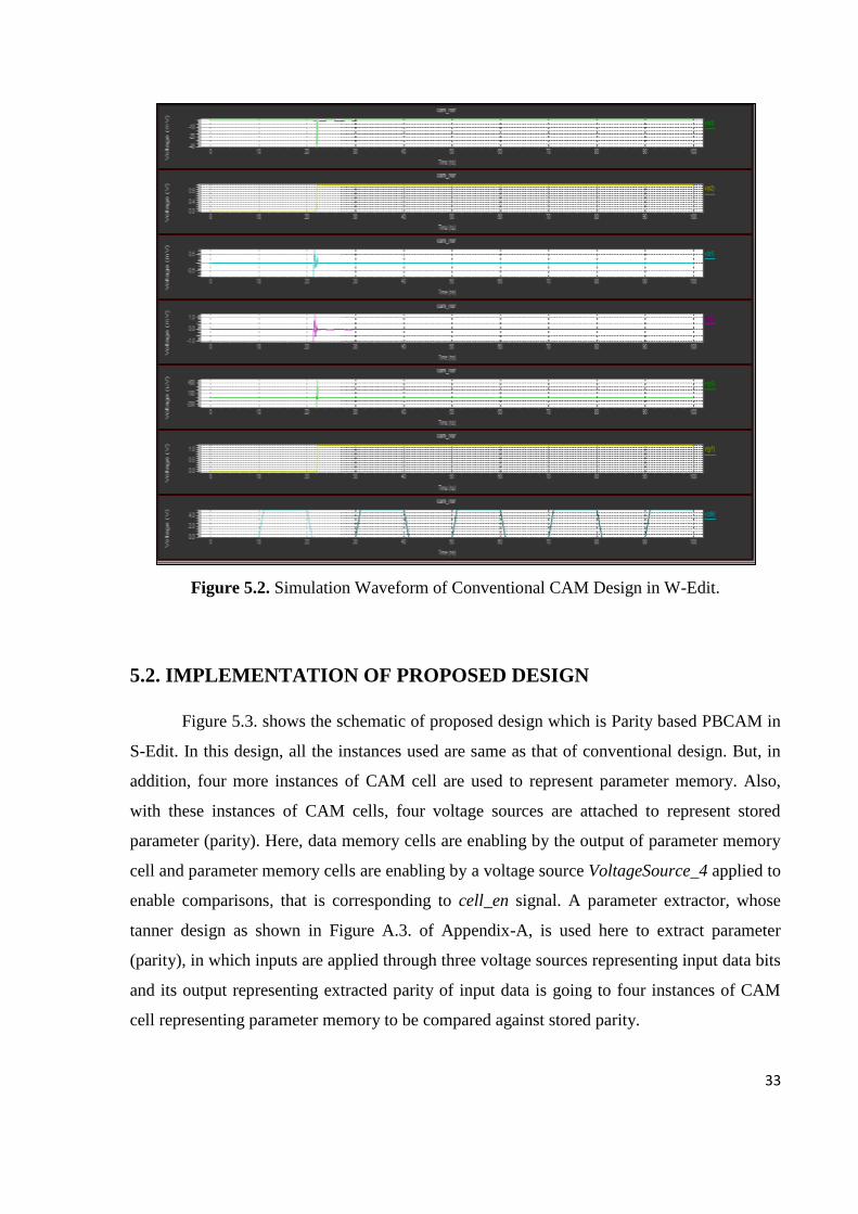
of Tanner EDA tool and waveform can be viewed in W-Edit as shown in Figure 5.2. In the
simulated waveform, last blue coloured waveform is representing clock (“clk”) signal. The
yellow and green coloured waveforms just above the “clk” are representing “y1” and “y0”,
respectively which are showing that data has been matched at the “10” location, where
“y1”=‘1’ and “y0”=‘0’. The four waveforms above the “y1” and “y0” are representing
matchlines “o0”, “o1”, “o2” and “o3”, showing that data has been matched at “o2”
matchline as “o2”=‘1’ and others are ‘0’ i.e. at third location “10”.
33
Figure 5.2. Simulation Waveform of Conventional CAM Design in W-Edit.
5.2. IMPLEMENTATION OF PROPOSED DESIGN
Figure 5.3. shows the schematic of proposed design which is Parity based PBCAM in
S-Edit. In this design, all the instances used are same as that of conventional design. But, in
addition, four more instances of CAM cell are used to represent parameter memory. Also,
with these instances of CAM cells, four voltage sources are attached to represent stored
parameter (parity). Here, data memory cells are enabling by the output of parameter memory
cell and parameter memory cells are enabling by a voltage source VoltageSource_4 applied to
enable comparisons, that is corresponding to cell_en signal. A parameter extractor, whose
tanner design as shown in Figure A.3. of Appendix-A, is used here to extract parameter
(parity), in which inputs are applied through three voltage sources representing input data bits
and its output representing extracted parity of input data is going to four instances of CAM
cell representing parameter memory to be compared against stored parity.

34
Figure 5.3. Schematic of Proposed Parity Bit based PBCAM in S-Edit.
The tanner design i.e. schematic shown in Figure 5.3. is now simulated using T-Spice
of Tanner EDA tool and waveform is viewed in W-Edit as shown in Figure 5.4. In the
simulated waveform, last blue coloured waveform is representing clock (“clk”) signal. The
yellow and green coloured waveforms just above the “clk” are representing “y1” and “y0”,
respectively which are showing that data has been matched at the “10” location, where
“y1”=‘1’ and “y0”=‘0’. The four waveforms above the “y1” and “y0” are representing
matchlines “o0”, “o1”, “o2” and “o3”, showing that data has been matched at “o2”
matchline as “o2”=‘1’ and others are ‘0’ i.e. at third location “10”.

35
Figure 5.4. Simulation Waveform of Proposed Parity Bit based PBCAM in W-Edit.
5.3. RESULTS
After implementing and simulating the proposed and conventional designs of CAM
using Tanner EDA Tool, we measured and compared the power consumptions and delays of
both the designs. Table 5.1. shows the power and delay comparisons of CAM architectures.
Table 5.1. Result Comparisons.
Parameters One’s Count
PBCAM [3]
Block-XOR
PBCAM [3]
Conventional
CAM
Proposed
PBCAM
TECHNOLOGY 0.35µm 0.35µm 0.13µm 0.13µm
POWER (mW) 266.84 146.48 61.02 33.24
DELAY (ns) 25 15 2.18 1.18
36
CHAPTER-6
CONCLUSION & FUTURE SCOPE
6.1. CONCLUSION
A parity based pre-computation based content addressable memory (PB-CAM) has
been proposed in which parity bit is used as a parameter. In the traditional CAM, a large
number of comparisons for accessing the CAM are creating a large amount of power
consumption. By proposed design, the number of comparisons in the data memory has been
reduced and hence power consumption and delay than the traditional CAM by little area
overhead. Moreover, parameter memory required for storing parameters and hence parameter
memory comparisons have been reduced than existing PBCAMs. So, parameter comparison
power and parameter memory area are also reduced than existing PBCAMs (One’s Count and
Block-XOR), making it efficient to implement and use practically. The proposed design has
been implemented using Tanner EDA Tool under 130nm technology. Simulation results are
showing that our proposed design achieves less power and high performance with 33.24mW
and 1.18ns respectively than the traditional CAM with 61.02mW and 2.18ns.
6.2. FUTURE SCOPE
In the future, we can reduce more power as compared to power and delay results of
proposed design. To reduce the results, we can use lower technology than 130nm. We can
also work on reducing the area of CAM. Work can also be done on extending these CAM
architecture designs to T-CAM.