Embed Size (px)
Citation preview

1
Chapter 1
Introduction
Recently, numerous publications [1]-[9] have reported some low-loss dielectric
and high-Q factor resonators/band-pass filters utilizing the substrate integrated
waveguide (SIW) technique or electromagnetic band-gap (EBG) technique. Such a
ideas of waveguides inherent the metallic waveguide, however, the solid metal walls
are replaced by the via-holes array. They can be fabricated by standard printed circuit
boards (PCBs) or the low temperature co-fired ceramics (LTCC) process. Similar
structures realized in the LTCC process are also known as laminated waveguide and
post-wall waveguide. It takes the advantages of low cost, low profile and good power
handling characteristic. Besides, it can be easily integrated into microwave and
millimeter wave integrated circuits. In comparison with microstrip-like structures, it
has higher Q-factor. In view of the above advantages, it is a good candidate for
realizing passive components in microwave and millimeter wave integrated circuits.
The cavity using the via-hole-wall technology was proposed and simulated in [1].
The three-dimensional integrated cavity resonators and filters consisting of via walls
using slot excitation with a quarter open stub was successfully demonstrated. A
multilayer Duroid realization of this filter was fabricated using standard printed
circuit board techniques in [2]. A high-Q performance, high-port isolation and
integrability to planar or 3-D circuit architectures filter, was demonstrated which was
implemented by via-holes technique.
The band-pass filter under consideration in this thesis is described as follow. The
band-pass filter consists of one cavity and input/output substrate integrated waveguide
utilizing via-hole array to approximate the metal wall. There are two apertures
2
connecting the two dielectric layers, each of which couples the energy (or signal)
between input (output) SIW waveguide and SIW cavity. The function of the cavity is
to sever as a Fabry-Parot resonator to filter the input signal. The cavity feeding
structure is a substrate integrated waveguide connecting with a taper micro-strip
transition. The filter was designed at the center frequency of 5.2GHz. The bandwidth
can be changed by the length of the aperture. The input and output waveguides was
isolated by placing the via-hole array.

3
Chapter 2
The basic concept of SIW
The classical waveguide technology is still the mainstream for designing
high-performance millimeter-wave systems. However, this matured scheme is not
suitable for low-cost mass-production. Tedious and expensive post-fabrication tuning
and assembling become a real problem for fabrication. In addition, the metallic
waveguide is hard to reduce its weight and volume. Thus the substrate integrated
waveguide (SIW) concept was developed and proved to be an attractive technology
for low-loss, low-cost, and high-density integration of microwave and
millimeter-wave components and subsystem.
The SIW technique makes it possible that a complete circuit including planar
circuitry, transitions, and rectangular waveguides are fabricated in planar form using a
standard printed circuit board or other planar processing techniques for widespread
applications. Such a class of waveguide been proved [10] [11] to be able to preserve
the well-known advantages of commonly used closed rectangular waveguide, such as
high-Q factor. Besides, the substrate integrated waveguide is based on printed circuit
board fabrication process; therefore, it is easy for being integrated with the micro-strip,
coplanar waveguide, or the other planar circuits, to design a microwave/millimeter
wave sub-system.

4
Figure 2.1 Configuration of the proposed transition of micro-strip line to rectangular
waveguide on the same substrate.
Fig. 2.2 (a) Rectangular waveguide
Fig. 2.2 (b) Micro-strip line
Figure 2.2 Dominant modal electric field profiles (a) in rectangular waveguide and (b)
in micro-trip line

5
Figure 2.1 shows the proposed transition from micro-strip line to rectangular
waveguide within the same dielectric substrate. The structure consists of a tapered
micro-strip line section that connects a 50Ωmicro-strip line and the integrated
waveguide. The tapering structure is used to transform the quasi-TEM mode of the
micro-strip line into the TE10 mode in the waveguide. As indicated in Figure 2.2, the
micro-strip line is suitably d to excite the waveguide because the electric fields of the
two dissimilar structures are approximately oriented in the same direction and share
the similar profile. The design criterion of such a taper transition is simple and
straightforward. It is well known that the propagation constant of the TE10 mode is
related to the width ”a” and relative dielectric constant. Since, the height or
thickness ”h” of the waveguide is smaller compared with width ”a”. Nevertheless,
reducing the height ”h” will increase the conductor loss in both the micro-strip line
and rectangular waveguide. Notice that at millimeter-wave frequencies, the
waveguide section is usually compact and then the conductor loss may be maintained
at a relatively low level.
A linearly tapered micro-strip is used, and this smooth transition ensures a field
matching between micro-strip and rectangular waveguide over a broad band-width.
The length “l” and width “d” of the taper, referring to Figure 2.1, should be modeled
and optimized over the desired frequency bandwidth.

6
Fig. 2.3 (a)
Fig. 2.3 (b)
Figure 2.3 On-substrate synthesized waveguide techniques: (a) metallic via-hole
arrays and (b) metallic walls.
7
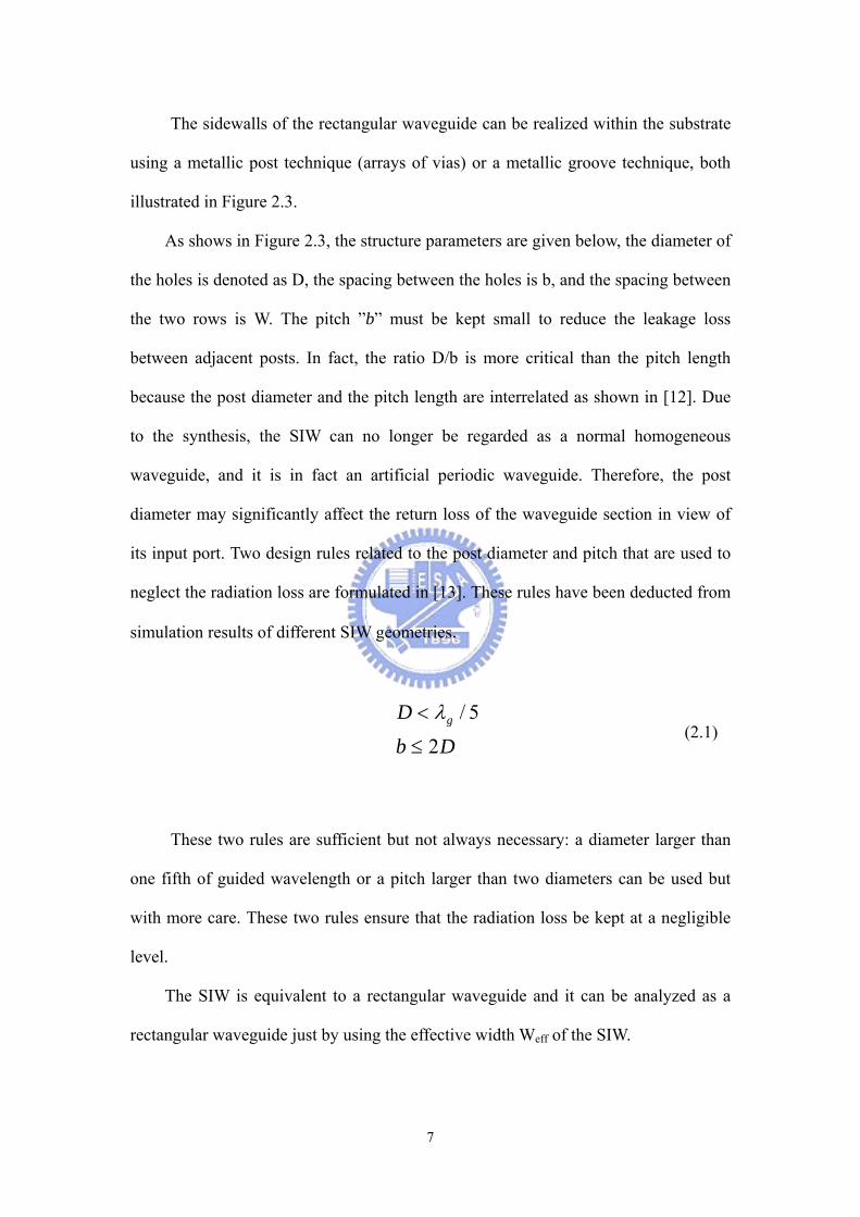
The sidewalls of the rectangular waveguide can be realized within the substrate
using a metallic post technique (arrays of vias) or a metallic groove technique, both
illustrated in Figure 2.3.
As shows in Figure 2.3, the structure parameters are given below, the diameter of
the holes is denoted as D, the spacing between the holes is b, and the spacing between
the two rows is W. The pitch ”b” must be kept small to reduce the leakage loss
between adjacent posts. In fact, the ratio D/b is more critical than the pitch length
because the post diameter and the pitch length are interrelated as shown in [12]. Due
to the synthesis, the SIW can no longer be regarded as a normal homogeneous
waveguide, and it is in fact an artificial periodic waveguide. Therefore, the post
diameter may significantly affect the return loss of the waveguide section in view of
its input port. Two design rules related to the post diameter and pitch that are used to
neglect the radiation loss are formulated in [13]. These rules have been deducted from
simulation results of different SIW geometries.
Db
D g
2
5/
≤
< λ (2.1)
These two rules are sufficient but not always necessary: a diameter larger than
one fifth of guided wavelength or a pitch larger than two diameters can be used but
with more care. These two rules ensure that the radiation loss be kept at a negligible
level.
The SIW is equivalent to a rectangular waveguide and it can be analyzed as a
rectangular waveguide just by using the effective width Weff of the SIW.

8
bDWWeff ×
−=95.0
2
(2.2)
provided that the spacing between the posts is sufficiently small.
Actually, Weff is decided by three parameters, namely, W, b, and D. However, the
modified term in (2.2) does not include the effect of D/W. when D increases, the small
error will appear. A more accurate empirical equation is proposed here as follows:
WD
bDWWeff
22
1.008.1 ×+×−= (2.3)
When b/D is smaller than three and D/W is smaller than 1/5, the empirical equations is
very accurate.
Although the SIW structures have similar properties as the conventional
rectangular waveguides, the differences between them are also obvious. First, the SIW
is a sort of periodic guided-wave structure, and it may lead to an electromagnetic
band-stop phenomenon. Second, the SIW structures are subject to a potential leakage
problem due to the periodic gaps. Therefore, the modes or waves traveling in the SIW
circuits are different from those in the normal waveguides and there exists a certain
type of leakage wave.

9
Chapter 3
Design of the SIW cavity band-pass filter
3-1 Rectangular cavity resonator
The proposed cavity resonators are based on the theory of rectangular cavity
resonators [14] and all designs and optimized with the aid of a CST Microwave
Studio. The cavity resonator is built utilizing conducting planes as horizontal walls
and via-hole-wall as sidewalls, as shown in Figure 3.1.
Figure 3.1 Cavity resonator utilizing via fences as sidewalls.
The diameter “D” and spacing “b” of via posts are properly chosen to prevent
electromagnetic field leakage and to achieve stop-band characteristic at the desired

10
resonant frequency. The resonant frequency of the TMmnl mode is obtained by
222
2⎟⎠⎞
⎜⎝⎛+⎟
⎠⎞
⎜⎝⎛+⎟
⎠⎞
⎜⎝⎛=
hp
ln
wmcf
sres
πππεπ
(3.1)
Where fres is the resonant frequency, c is the speed of light, εr is the dielectric constant,
“l” is the length of the cavity, “w” is the width of the cavity, and “h” is the height of
the cavity. Using (3.1), the initial dimensions of the cavity with perfectly conducting
walls are determined for a resonant frequency of 5.2GHz for the TM110 dominant
mode by simply indexing m=1, n=1, p=0 and optimized with a full-wave
electromagnetic simulator (w=17mm, l=17mm, h=0.508mm). The design parameters
of the feeding structures are then slightly modified to achieve the best performance in
term of low insertion loss and accurate resonant frequency.
To decrease the metal loss and enhance the Q factor, the vertical conducting walls
are replaced by a lattice of via posts. In our case, we used Cassivi’s expressions [7] to
get the preliminary design values, and then the final dimensions of the cavity are fine
tuned with the CST microwave studio simulator. The spacing ”b” between the via
posts of the sidewalls is limited to less than half guided wavelength (λg/2) at the
highest frequency of interest so that the radiation losses becomes negligible.
In the case of low external coupling, the unloaded Q (Qu) is controlled by three
loss mechanisms and is defined by
1111
−
⎟⎟⎠
⎞⎜⎜⎝
⎛++=
raddieleccondu QQQ
Q (3.2)
Where Qcond, Qdielec, and Qrad take into account the conductor loss from the horizontal

11
plates (the metal loss of the horizontal plates dominates, especially for a thin substrate
such as 0.508mm), the dielectric loss from the filling substrates, and the leakage loss
through the via walls, respectively. Since the gap between the via posts is less than
λg/2 at the highest frequency of interest as mentioned, the leakage (radiation) loss can
be negligible as mentioned above and the individual quantity of two other Q factors
can be obtained from [15]
( )wllwhlhwRhkwlQ
mcond 33332
3
222)(
+++=
πη (3.3)
Where
w, l and h effective cavity width, length and height, respectively:
η wave impedance;
k wave number in the resonator ((2πfres(εr)1/2)/c);
Rm surface resistance of the cavity ground planes ((πfresµ/σ)1/2);
)tan(1δ
=dielecQ (3.4)
Where tan δ is the loss tangent of the substrate.
In the chapter 4, simulation results of the SIW cavity are given. From the results,
we can see that the power leakage via the gaps of the SIW cavity is much smaller than
that from the conductor loss and the dielectric dissipation in the total power
dissipation when certain conditions are satisfied.

12
3-2 The band-pass filter structure
Figure 3.2 (a)-(b) show that the top layer and bottom layer band-pass filter
structure, respectively. This band-pass filter consists of two dielectric layers. The top
layer contains the input and output via-hole-wall waveguides and the bottom layer
contains a via-hole-wall cavity. The electromagnetic field coupling between the
via-hole-wall waveguide and cavity is through the two apertures etched on the top
surface of the cavity, and on the bottom surface of the waveguides, as well. The two
input/output waveguides was isolated by placing the via-hole array between them.
Notice that the pitch of the via-hole array separating the input and output waveguides
should be kept as small as possible for preventing the direct coupling between the two
waveguides. Besides, the input and output via-hole-wall waveguides are fed,
respectively, by the micro-strip line with linear taper transition. The waveguide side
walls or cavity walls are made from the double rows of via-wall to reduce the
electromagnetic wave leakage.
Fig. 3.2 (a)

13
Fig. 3.2 (b)
Figure 3.2 3-D overview of band-pass filter structure (a) first layer (b) second layer

14
Chapter 4
Simulation and measurement results
In this thesis, we were carried out using the CST Microwave Studio for the
scattering characteristics. This simulation software is base on the Finite Integration
Technique (FIT) in time domain. The band-pass filter was fabricated using microwave
substrate RO4003, relative dielectric constant εr=3.38, thickness 0.508mm, loss
tangent tanδ=0.0027. The via-hole arrays were implemented using electronic plating
technique. The measurement is performed using an HP8722D network analyzer.
Figure 4.1 (a)-(d) show that the parameters for the every layer structure. Their
sizes were listed in the table 1. Figure 4.1 (a)-(b) depicted the top side and bottom side
of the first layer for the band-pass filter structure, respectively. The top side included
the input and output via-hole-wall waveguides that are fed by the micro-strip line with
linear taper transition. Between the input and the output waveguide was isolated by
placing the via-hole array. The bottom of the first layer etched two apertures. Figure
4.1 (c)-(d) show that the top side and bottom side of the second layer, respectively. In
the resonant cavity, the top side of the second layer including two coupling apertures
that the electromagnetic field coupling is taking place between the substrate integrated
waveguide and the cavity resonator.

15
Fig. 4.1 (a)
Fig. 4.1 (b)

16
Fig. 4.1 (c)
Fig 4.1 (d)
Figure 4.1 Structure configuration of the SIW band-pass filter using via-hole arrays;
(a): first layer (top side) including two via-hole-wall waveguide, (b): bottom side, (c):
top side of the second layer including two coupling apertures in the resonant cavity,
and (d): bottom side of the resonant cavity.

17
radius of via hole: r 0.5 mm
width of waveguide (cavity width): wy 17 mm
via-hole array (waveguide wall) pitch: p1 1 mm
via-hole array (partition wall) pitch: p2 0.55 mm
via-hole array (the second row) pitch: p3 0.8 mm
aperture length: ay 17 mm
aperture width: ax 0.6 mm
input/output waveguide length: lwg 7.3 mm
cavity length: wx 17 mm
cavity length: wy 15 mm
micro-strip line width: ws 1.2 mm
micro-strip line length: ls 3 mm
taper transition width: tw 9 mm
taper transition length: tl 1.7 mm
Table 4.1 Structure parameter

18
Table 4.1 indicates that the band-pass filter size. The width of the waveguide is
17 mm. The cutoff frequency fmn can be easily obtained by
22
21
⎟⎠⎞
⎜⎝⎛+⎟
⎠⎞
⎜⎝⎛=
bn
amf ππ
εµπ (4.1)
Where the integer m and n denote the index number along width and height direction,
respectively. Since the width of the waveguide is far larger than the height. Therefore,
the propagation mode is TE10. Figure 4.2 shows that the cutoff frequency is 4.03 GHz
by high-pass filter. The cutoff frequency is lower than that we developed pass-band
frequency of the band-pass filter. The calculation of the equivalent width Weff is given
in Chapter 2 above, then into the (4.1) can be also calculated the cutoff frequency.
Figure 4.2 Simulated insertion loss for the substrate integrated waveguide with
waveguide width 17 mm

19
Figure 4.3 is the simulated result of the band-pass filter with changing the length
of the aperture while keeping all the other parameters. Form these figures, we found
that the bandwidth of the band-pass filter can be altered by changing the length of the
aperture. When the bandwidth is increasing as the aperture length is increased. It may
be conjectured that due to the increase in the length of coupling aperture the coupling
coefficient between the waveguide and cavity increases accordingly. The return loss
and the return loss are presented in Figure 4.3 (a) and Figure 4.3 (b) respectively.
Figure 4.4 (a)-(b) show the variation of return loss and insertion loss versus
frequency for various position of aperture. The positions of the two coupling aperture
have to be properly designed to achieve a good performance in scattering parameters.
The distance of aperture relative to the first layer centerline form 4.2 mm to 5.7 mm is
shown in Figure 4.4(a) and (b). From these figures, the positions of the two coupling
aperture are more close to the first layer centerline that the stop-band bandwidth will
become significantly large. However, the return loss is more than -10 dB.

20
Fig.4.3 (a)

21
Fig 4.3 (b)
Figure 4.3 The simulation of the tunable band-pass filter with the length of aperture
(a) return loss (b) insertion loss

22
Fig. 4.4 (a)

23
Fig. 4.4 (b)
Figure 4.4 The simulation of the tunable band-pass filter with the distance of aperture
(a) return loss (b) insertion loss

24
As shown in Figure 4.5 (a)-(d), the band-pass filter is designed, fabricated on a
standard PCB process using via-hole-wall. The Figure 4.6 shows that photo of the
proposed band-pass filter which combined first layer with second layer with screw.
Figure 4.7 depicted the measured and simulated results for the insertion and
return loss of the band-pass filter. The two coupling apertures share the same width
and length, which are 0.6 mm and 17 mm, respectively. The length, width and
thickness of the resonance cavity are 15 mm, 17 mm and 0.508 mm, respectively. The
dashed lines denote the measured result, while the solid lines represent the simulated
result. The band-pass filter exhibits an insertion loss about -1.59 dB, which is slightly
higher than simulated value of -0.47dB, and a return loss <-10.3 dB compared to a
simulated value <-16.6dB over the pass-band shown in Figure 4.7. The measured
results give a 3-dB bandwidth of 36.8% at a center frequency of 5.4GHz. Since the
thickness of the cavity is far smaller than the width and length, the major component
of the electric field in the cavity is Ez, while the Ex and Ey are negligible. Therefore,
the lowest resonant mode is TM110 in this example. The resonant frequency for the (m,
n, o) mode of the cavity without apertures is given below
( ) ( ) slnwmGHzinf ε///150)( 22 += (4.2)
Where the integer m and n denote the index number along width and length direction,
respectively. We use equation (4.2) to obtain the resonant frequency is about 6.44
GHz. The relative dielectric constant of the substrate is characterized by εs. However,
due to the existence of two coupling apertures, the resonance frequency should be
different with the value given in (4.2). From Figure 4.7, it is obvious to see that the
excellent agreement between the simulated and measured results.

25
As mentioned earlier, the band-pass characteristics of this filter is based on the
resonance effect of the cavity. To prove that the band-pass characteristic is due to the
resonant mode, TM110, we plot the contour map, depicted in Figure 4.8, for the
vertical component of electric field strength (Ez) on the cross section at z=0.5h (h is
the thickness of the substrate) at the resonant frequency (5.4GHz). Form this figure, it
is apparently to see that the maximum electric field is around the center of the cavity
and the field variation resembles the function given below.
( )yx
z wy
wxyxE ππ sinsin, ≈ (4.3)
It is clearly observed that double rows of via-wall are sufficient to block the
electromagnetic field leakage through the vias.
Fig. 4.5 (a)

26
Fig. 4.5 (b)
Fig. 4.5 (c)

27
Fig. 4.5 (d)
Figure 4.5 The layout of the band-pass filter (a) top view of the first layer (b) bottom
view (c) top view of the second layer (d) bottom view showing the resonant cavity.
Fig. 4.6 (a)

28
Fig. 4.6 (b)
Figure 4.6 Photo of the proposed band-pass filter.(a) top view (b) bottom view.

29
Figure 4.7 measured and simulated insertion and return loss for the band-pass filter
with aperture length 17 mm.

30
Figure 4.8 Distribution of the field contour (Ez component) inside the resonant cavity
over the cross section at the position z =0.5h, where h is the thickness of the substrate.
In the following two examples, we change the aperture length while keeping all
the other parameters given in the previous example. The lengths of the aperture are 15
mm and 13 mm in Figure 4.9 and 4.10. Comparing Figure 4.9 and 4.10 with Figure
4.7, it is apparently to see that the bandwidth is decreasing as the aperture length is
decreased. It is noted that the insertion loss in Figure 4.10 increases, compared with
those in Figure 4.7 and 4.9. It may be conjectured that due to the decrease in the
length of coupling aperture the coupling coefficient between the waveguide and cavity
decreases accordingly. The bandwidth of the three cases shown in Figure 4.7, 4.9 ,
4.10 and 4.11 are 36.8%, 32.9%, 31.3% and 12.8%, respectively. Figure 4.10 show
that insertion loss about -2dB was larger than the insertion loss of the aperture length
17mm and 15mm. We found that the bandwidth decreases as the decrease in the

31
aperture length, however, the insertion loss increases. We have also carried out the
numerical simulations and experimental studies for the cases with several different
aperture lengths.
Figure 4.9 Measured and simulated insertion and return loss for the band-pass filter
with aperture length 15mm.

32
Figure 4.10 Measured and simulated insertion and return loss for the band-pass filter
with aperture length 13mm.

33
Figure 4.11 Measured and simulated insertion and return loss for the band-pass filter
with aperture length 8mm.

34
Chapter 5
Conclusion
A novel band-pass filter using a resonant cavity based on the via-hole-wall
technology has been developed. The pass-band frequency can be estimated by the
resonant frequencies of the cavity. Besides, the bandwidth of this band-pass filter can
be altered by turning the length of coupling aperture. Due to the vertical coupling
between the substrate integrated waveguide and cavity, the size of the structure is
further reduced. Measured and simulated results using CST Microwave Studio have
been presented and discuss. A good agreement between the measured and simulation
results was obtained. Such types of filter are valuable in the design and realization of
low-cost microwave and millimeter wave system.

35
Reference
[1] Jong-Hoon Lee, Stephane Pinel, John Papapolymerou, Joy Laskar and Manos M.
Tentzeris, “ Low-loss LTCC cavity filters using system -on-package technology at
60 GHz ” IEEE Trans. Microw. Theory Tech., vol. 53, no. 12, pp.3817-3824,
December, 2005
[2]H. J. Hsu, M. J. Hill, J. Papaolymerou, and R. W. Ziolkowski, “ A planar X-band
electromagnetic bandgap (EBG) 3-pole filter,” IEEE Microw. Wireless Compon.
Lett., vol. 12, no. 7, pp. 255-257, Jul. 2002.
[3]W. Chappell, M. Little, and L. Katehi, “High isolation, planar filters using EBG
substrates.” IEEE Microwave Wireless Compon. Lett., vol. 11, pp. 246-248, June
2001.
[4] M. J. Hill, R. W. Ziolkowski, and J. Papapolymerou, “Simulated and measured
results from a Duroid-based planar MBG cavity resonator filter,” IEEE Microw.
Wireless Compon. Lett. vol. 10, no. 12, pp.528-530, Dec. 2000.
[5]C. A. Tavernier, R. M. Henderson, and J. Papapolymerou, “A reduced- size silicon
micromachined high-Q resonator at 5.7GHz,” IEEE Trans. Microw. Theory Tech.,
vol. 50, no. 10, pp. 2305-2314, Oct. 2002.
[6]Yu Lin Zhang, Wei Hong, Ke Wu, Ji Xin, Chen and Hong Jun Tang, “Novel
Substrate Integrated Waveguide Cavity Filter with Defected Ground Structure,”
IEEE Trans. Microw. Theory Tech., vol 53, no. 4, pp. 1280-1287, April. 2005.
[7]Y. Cassivi and K. Wu,”Low cost microwave oscillator using substrate integrated
waveguide cavity,” IEEE Microw. Wireless Compon. Lett., vol. 13, no. 2, pp.
48-50, F eb. 2003.
[8]Yu Lin Zhang, Wei Hong, Ke Wu, Ji Xin, Chen and Zhang Cheng Hao,

36
“Development of compact bandpass filters with SIW triangular cavities,”
Microwave Conference Proceedings, 2005. APMC 2005. Asia-Pacific Conference
Proceedings, Volume 1, Issue , 4-7 Dec. 2005 Page(s): 4 pp.,
[9]Z. C. Hao, W. Hong, X. P. Chen, J. X. Chen, K. Wu, and T. J. Cui, “Multilayered
substrate integrated waveguide (MSUBSTRATE INTEGRATED WAVEGUIDE)
elliptic filter,” IEEE Microw. Wireless Compon. Lett., vol. 15, no. 2,pp. 95-97, Feb.
2005.
[10]Feng Xu and Ke Wu, “Guided-Wave and Leakage Characteristics of Substrate
Integrated Waveguide,” IEEE Trans. Microw. Theory Tech., vol. 53, no. 1, pp.
66-73, Jan. 2005.
[11]Y.Cassivi, L. Perregrini, P. Arcioni, M. Bressan, K. Wu, and G. Conciauro,
“Dispersion characteristics of substrate integrated rectangular waveguide,” in
IEEE Microwave Wireless Compon. Lett., vol. 12, Sep. 2002, pp. 333-335.
[12]D. Deslandes and K. Wu. “Single-substrate integration techniques for planar
circuits and waveguide filters”, IEEE Transactions on Microwave Theory and
Techniques, Feb. 2003, pp. 593-596.
[13]D. Deslandes and K. Wu. “Design consideration and performance analysis of
substrate integrated waveguide components”, Milano, European Microwave
Conference, 23-27. Sept. 2002. pp. 881-884.
[14]R. E. Collin, Foundations for Microwave Engineering. New York: Mc-Graw-Hill,
1992.
[15]D. M. Pozar, Microwave Engineering, 2ed. New York: Wiley, 1998.