Embed Size (px)
Citation preview

7/23/2019 Chapter 1- Semiconductor Diodes
http://slidepdf.com/reader/full/chapter-1-semiconductor-diodes 1/31
1
Chapter 1:
Semiconductor Diodes

7/23/2019 Chapter 1- Semiconductor Diodes
http://slidepdf.com/reader/full/chapter-1-semiconductor-diodes 2/31
2
DiodesDiodes
The diode is a 2-terminal device.
A diode ideally conducts in only one direction.

7/23/2019 Chapter 1- Semiconductor Diodes
http://slidepdf.com/reader/full/chapter-1-semiconductor-diodes 3/31
3
Diode CharacteristicsDiode Characteristics
Conduction RegionConduction Region
• The voltage across the diode is 0 V
• The current is infinite
• The forward resistance is defined as
R F = V
F/ I
F
• The diode acts like a short
Non-Conduction RegionNon-Conduction Region
•
All of the voltage is across the diode• The current is 0 A
• The reverse resistance is defined as
R R = VR / IR
• The diode acts like open

7/23/2019 Chapter 1- Semiconductor Diodes
http://slidepdf.com/reader/full/chapter-1-semiconductor-diodes 4/31
4
Semiconductor MaterialsSemiconductor Materials
Materials commonly used in the
development o semiconductor
devices:
• ilicon !i"ilicon !i"
• #alliu$ nitride !#a%"#alliu$ nitride !#a%"
• &inc o'ide !&n("&inc o'ide !&n("
• #er$aniu$ !#e"#er$aniu$ !#e"
• #alliu$ Arsenide !#aAs"#alliu$ Arsenide !#aAs"

7/23/2019 Chapter 1- Semiconductor Diodes
http://slidepdf.com/reader/full/chapter-1-semiconductor-diodes 5/31
5
DopingDoping
The electrical characteristics o silicon and germanium areimproved !y adding materials in a process called doping.
There are "ust t#o types o doped semiconductor materials:
nn)type)type
p p)type)type
• n)type $aterials contain an e'cess of conduction *and
electrons.
• p)type $aterials contain an e'cess of valence *and holes.

7/23/2019 Chapter 1- Semiconductor Diodes
http://slidepdf.com/reader/full/chapter-1-semiconductor-diodes 6/31
6
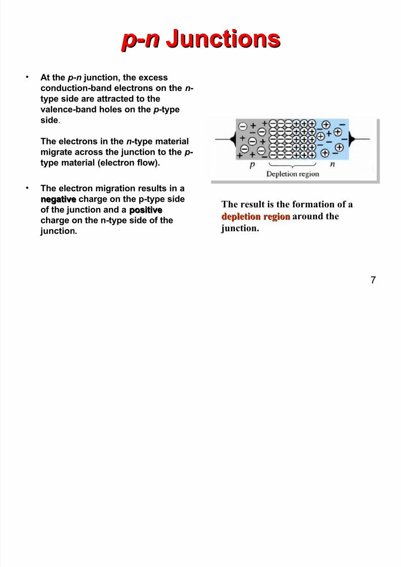
p-n p-n $unctions$unctions
(ne end of a silicon or ger$aniu$ crystal can *e doped
as a p)type $aterial and the other end as an n)type
$aterial.
The result is a p-n p-n +unction +unction.
7/23/2019 Chapter 1- Semiconductor Diodes
http://slidepdf.com/reader/full/chapter-1-semiconductor-diodes 7/31
7
p-n p-n $unctions$unctions
• %t the p-n "unction& the e'cess
conduction-!and electrons on the n-
type side are attracted to the
valence-!and holes on the p-type
side.
The electrons in the n-type materialmigrate across the "unction to the p-
type material (electron lo#).
• The electron migration results in a
negativenegative charge on the p-type side
o the "unction and a positivepositivecharge on the n-type side o the
"unction.
The result is the for$ation of a
depletion regiondepletion region around the
+unction.

7/23/2019 Chapter 1- Semiconductor Diodes
http://slidepdf.com/reader/full/chapter-1-semiconductor-diodes 8/31
8
Diode *perating ConditionsDiode *perating Conditions
% diode has three operating conditions:
• %o *ias
•
Forward *ias• Reverse *ias

7/23/2019 Chapter 1- Semiconductor Diodes
http://slidepdf.com/reader/full/chapter-1-semiconductor-diodes 9/31
9
Diode *perating ConditionsDiode *perating Conditions
No +iasNo +ias
• %o e'ternal voltage is applied, V D
= 0 V
• %o current is flowing, I D = 0 A
• (nly a $odest depletion region e'ists

7/23/2019 Chapter 1- Semiconductor Diodes
http://slidepdf.com/reader/full/chapter-1-semiconductor-diodes 10/31
10
Diode *perating ConditionsDiode *perating Conditions
Reverse +iasReverse +ias
-'ternal voltage is applied across the p-n +unction in
the opposite polarity of the p) and n)type $aterials.
• The reverse voltage causes the
depletion region to widen.
• The electrons in the n)type $aterial
are attracted toward the positiveter$inal of the voltage source.
• The holes in the p)type $aterial areattracted toward the negativeter$inal of the voltage source.

7/23/2019 Chapter 1- Semiconductor Diodes
http://slidepdf.com/reader/full/chapter-1-semiconductor-diodes 11/31
11
Diode *perating ConditionsDiode *perating Conditions
,or#ard +ias,or#ard +ias
-'ternal voltage is applied across the p-n +unction in
the sa$e polarity as the p) and n)type $aterials.
• The forward voltage causes the depletionregion to narrow.
• The electrons and holes are pushedtoward the p-n +unction.
• The electrons and holes have sufficient
energy to cross the p-n +unction.

7/23/2019 Chapter 1- Semiconductor Diodes
http://slidepdf.com/reader/full/chapter-1-semiconductor-diodes 12/31
12
%ctual Diode Characteristics%ctual Diode Characteristics
%ote the regions for no
*ias reverse *ias and
forward *ias conditions.
arefully note the scale
for each of these
conditions.

7/23/2019 Chapter 1- Semiconductor Diodes
http://slidepdf.com/reader/full/chapter-1-semiconductor-diodes 13/31
13
Ma"ority and Minority CarriersMa"ority and Minority Carriers
T#o currents through a diode:
a+ority arriersa+ority arriers
• The $a+ority carriers in n)type $aterials are electrons.
• The $a+ority carriers in p)type $aterials are holes.
inority arriersinority arriers
• The $inority carriers in n)type $aterials are holes.
• The $inority carriers in p)type $aterials are electrons.

7/23/2019 Chapter 1- Semiconductor Diodes
http://slidepdf.com/reader/full/chapter-1-semiconductor-diodes 14/31
14
ener Regionener Region
• The ener region is in thediodes reverse-!ias region.
• %t some point the reverse!ias voltage is so large the
diode !rea/s do#n and thereverse current increasesdramatically.
• The $a'i$u$ reverse voltage that won1t take a diode
into the 2ener region is called the peak inverse voltagepeak inverse voltage
or peak reverse voltagepeak reverse voltage.
• The voltage that causes a diode to enter the 2ener
region of operation is called the 2ener voltage !V2ener voltage !V&&"".

7/23/2019 Chapter 1- Semiconductor Diodes
http://slidepdf.com/reader/full/chapter-1-semiconductor-diodes 15/31
15
,or#ard +ias 0oltage,or#ard +ias 0oltage
The point at #hich the diode changes rom no-!iascondition to or#ard-!ias condition occurs #hen theelectrons and holes are given suicient energy tocross the p-n "unction. This energy comes rom the
e'ternal voltage applied across the diode.
The forward *ias voltage re3uired for a,
• galliu$ arsenide diode 4.5 V
• silicon diode 0.6 V
• ger$aniu$ diode 0.7 V

7/23/2019 Chapter 1- Semiconductor Diodes
http://slidepdf.com/reader/full/chapter-1-semiconductor-diodes 16/31
16
Temperature ectsTemperature ects
• %s temperature increases it adds energy tothe diode.
• t reduces the re3uired or#ard !ias voltageor or#ard-!ias conduction.
• t increases the amount o reverse current inthe reverse-!ias condition.
• t increases ma'imum reverse !iasavalanche voltage.
• 4ermanium diodes are more sensitive totemperature variations than silicon orgallium arsenide diodes.

7/23/2019 Chapter 1- Semiconductor Diodes
http://slidepdf.com/reader/full/chapter-1-semiconductor-diodes 17/31
17
Resistance 5evelsResistance 5evels
• Semiconductors react dierently to DC
and %C currents.
• There are three types o resistance:
6 DC (static) resistance6 %C (dynamic) resistance
6 %verage %C resistance

7/23/2019 Chapter 1- Semiconductor Diodes
http://slidepdf.com/reader/full/chapter-1-semiconductor-diodes 18/31
18
DC (Static) ResistanceDC (Static) Resistance
,or a speciic applied DC voltage V D& the diode
has a speciic current I D& and a speciic
resistance R D.
D
DD
I
VR =

7/23/2019 Chapter 1- Semiconductor Diodes
http://slidepdf.com/reader/full/chapter-1-semiconductor-diodes 19/31
19
%C (Dynamic) Resistance%C (Dynamic) Resistance
n the or#ard !ias region: B
D
d r I
r +=′$V58
• The resistance depends on the a$ount of current ! I D
" in the diode.
• The voltage across the diode is fairly constant !58 $V for 59°".
• r B
ranges fro$ a typical 0.4 for high power devices to 5 for low
power general purpose diodes. In so$e cases r B
can *e ignored.
In the reverse *ias region,∞ rd
The resistance is effectively infinite. The diode acts like an open.

7/23/2019 Chapter 1- Semiconductor Diodes
http://slidepdf.com/reader/full/chapter-1-semiconductor-diodes 20/31
20
%verage %C Resistance%verage %C Resistance
pt.topt. d
d
av
ΔI
ΔV r =
A resistance can *e
calculated using thecurrent and voltage
values for two points on
the diode characteristic
curve.
7/23/2019 Chapter 1- Semiconductor Diodes
http://slidepdf.com/reader/full/chapter-1-semiconductor-diodes 21/31
21
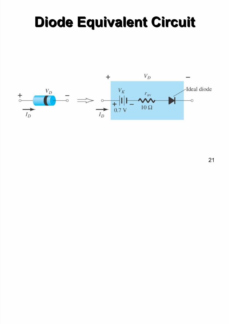
Diode 3uivalent CircuitDiode 3uivalent Circuit

7/23/2019 Chapter 1- Semiconductor Diodes
http://slidepdf.com/reader/full/chapter-1-semiconductor-diodes 22/31
22
Diode CapacitanceDiode Capacitance
In reverse *ias the depletion layer is very large. The diode1s strong positive and
negative polarities create capacitance T. The a$ount of capacitance depends
on the reverse voltage applied.
In forward *ias storage capacitance or diffusion capacitance !:" e'ists as the
diode voltage increases.

7/23/2019 Chapter 1- Semiconductor Diodes
http://slidepdf.com/reader/full/chapter-1-semiconductor-diodes 23/31
23
Reverse Recovery Time (trr)Reverse Recovery Time (trr)
Reverse recovery ti$eReverse recovery ti$e is the ti$e re3uired for a diode to
stop conducting once it is switched fro$ forward *ias to
reverse *ias.

7/23/2019 Chapter 1- Semiconductor Diodes
http://slidepdf.com/reader/full/chapter-1-semiconductor-diodes 24/31
24
Diode Speciication SheetsDiode Speciication Sheets
:ata a*out a diode is presented unifor$ly for $any different diodes. This$akes cross)$atching of diodes for replace$ent or design easier.
4. Forward Voltage !VF" at a specified current and te$perature
5. a'i$u$ forward current !IF" at a specified te$perature
7. Reverse saturation current !IR " at a specified voltage and
te$perature
;. Reverse voltage rating or V!<R" at a specified te$perature
9. a'i$u$ power dissipation at a specified te$perature8. apacitance levels
6. Reverse recovery ti$e , t rr
. (perating te$perature range

7/23/2019 Chapter 1- Semiconductor Diodes
http://slidepdf.com/reader/full/chapter-1-semiconductor-diodes 25/31
25
Diode Chec/er Diode Chec/er
any digital $ulti$eters have a diode checking function.
The diode should *e tested out of circuit.
A nor$al diode e'hi*its its forward voltage,
• #alliu$ arsenide 4.5 V
• ilicon diode 0.6 V
• #er$aniu$ diode 0.7 V
7/23/2019 Chapter 1- Semiconductor Diodes
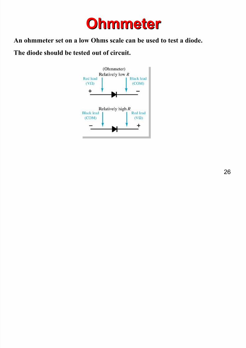
http://slidepdf.com/reader/full/chapter-1-semiconductor-diodes 26/31
26
*hmmeter *hmmeter An oh$$eter set on a low (h$s scale can *e used to test a diode.
The diode should *e tested out of circuit.

7/23/2019 Chapter 1- Semiconductor Diodes
http://slidepdf.com/reader/full/chapter-1-semiconductor-diodes 27/31
27
Curve Tracer Curve Tracer
A curve tracer displays the characteristic curve of a diode in thetest circuit. This curve can *e co$pared to the specifications of
the diode fro$ a data sheet.

7/23/2019 Chapter 1- Semiconductor Diodes
http://slidepdf.com/reader/full/chapter-1-semiconductor-diodes 28/31
28
*ther Types o Diodes*ther Types o Diodes
• ener diode
• 5ight-emitting diode
•Diode arrays

7/23/2019 Chapter 1- Semiconductor Diodes
http://slidepdf.com/reader/full/chapter-1-semiconductor-diodes 29/31
29
ener Diodeener Diode
• % ener is a diode operated in reverse
!ias at the ener voltage (0).
• Common ener voltages are !et#een
1.7 0 and 288 0

7/23/2019 Chapter 1- Semiconductor Diodes
http://slidepdf.com/reader/full/chapter-1-semiconductor-diodes 30/31
30
5ight-mitting Diode (5D)5ight-mitting Diode (5D)
An >-: e$its photons when it is forward *iased.
These can *e in the infrared or visi*le spectru$.
The forward *ias voltage is usually in the range of 5 V to 7 V.

7/23/2019 Chapter 1- Semiconductor Diodes
http://slidepdf.com/reader/full/chapter-1-semiconductor-diodes 31/31
31
Diode %rraysDiode %rrays
ultiple diodes can *e packaged togetherin an integrated circuit !I".
Common %nodeCommon %node
Common CathodeCommon CathodeA variety of co$*inations
e'ist.