Embed Size (px)
Citation preview

LOGO
INTRODUCTION TO SEMICONDUCTOR
CHAPTER 1CHAPTER 1
EE 201 – SEMICONDUCTOR DEVICES
BYPN. RUHIYAH NAZIHAH ZAHKAI
ELECTRICAL ENGINEERING DEPARTMENTPOLYTECHNIC SULTAN IDRIS SHAH

COURSE LEARNING OUTLINE
At the end of this course, you will be able to : Describe illustratively the theoretical characteristics
and electrical properties of semiconductors. (C2)
Explain the applications of semiconductor devices using the schematic diagrams. (C4)
Conduct the construction of semiconductor devices application circuits based on schematic diagrams. (P4)

Objectives
At the end of the lesson, students should be able to:-
1.1 Understand the characteristics and electrical
properties of semiconductors.
1.1.1 Define a semiconductor and state that silicon and
Germanium are semiconductor materials.
1.1.2 Explain the characteristics of N-type and P- type
semiconductors.

ATOMIC STRUCTURE
All matters on earth made of atoms (made up of elements or combination of elements).
All atoms consist of electrons, protons, and neutrons.
An atom is the smallest particle of an element that retains the characteristics of that element.

Bohr’s Atomic Structure
According to Bohr, atoms have a planetary structure that consists of a central nucleus, surrounded by orbiting electrons.
Nucleus contains protons and neutrons.
• The ability of a material to conduct current is based on its atomic structure.
• The orbit paths of the electrons surrounding the nucleus are called shells.
• Each shell has a defined number of electrons it will hold.(2xn2)Ex:Copper:2.8.18.1 (electron valence)
• The outer shell is called the valence shell and electrons at this layer are called valence electrons.
• Maximum number of valence electron is 8
• The less complete a shell is filled to capacity the more conductive the material is

The valence shell determines the ability of material to conduct current.
• Copper atom has only 1 electron in its valence ring. This makes it a good conductor.
• Silicon atom has 4 electrons in its valence ring. This makes it a semiconductor.

CONDUCTOR
An atom of a material carries 1 to 3 valence electrons.
Any material that will support a generous flow of charge when a voltage source is applied across its terminals.
the atom has more tendency to lose its valence electrons which become free electron (Copper,Aluminium)

INSULATOR
An atom of a material carries 5 to 8 valence electron
A material that offers a very low level of conductivity under pressure from an applied voltage source.
The atom has more tendency to gain free electrons to complete its shell. ( Argon, Neon)

SEMICONDUCTOR
An atom of a material carries 4 valence electrons,
A material that has a conductivity level somewhere between a conductor and an insulator.
It is not easy for the atom to lose or gain any electrons. (Silicon, Germanium, Carbon)

SEMICONDUCTOR MATERIAL
Figure 1.3Carbon (6 electrons)
Shell valence consist of 4 electron valence 6
Figure 1.2Silicon (14 electrons)
Figure 1.3Germanium (32
electrons)
Shell valence consist of 4 electron valence
1432

COVALENT BOND
In a pure silicon or germanium crystal, the four valence electrons of one atom form a bonding arrangement with four adjoining atoms.
This bonding of atoms, strengthened by the sharing of electrons, is called covalent bonding – a method by which atoms complete their valence shell by sharing valence electrons with other atoms

COVALENT BOND
The atoms areelectrically stablebecause their valenceshells are complete.
The center silicon atoms share an electron share each of the four surrounding atoms creating covalent band with each

CONDUCTOR IN SEMICONDUCTOR
When an intrinsic silicon crystal gains sufficient heat (thermal energy), some valence electrons could break their covalent bonds to jump the gap into conduction band, becoming free electrons.
Free electrons are also called conduction electrons, (negative charge).
This vacancy in the valence band is called a hole (positive charge).

• For every electron raised to the conduction band, there is 1 hole in the valence band creating – electron-hole pair.
• When a conduction electron loses energy and falls back into a hole, this is called recombination.
• With the existence of holes and electrons, current can be produced when a voltage is applied across the terminals.

INTRINSIC AND EXTRINSIC SEMICONDUCTOR
Intrinsic (pure) materials are those semiconductors that have been carefully refined to reduce the impurities to a very low level.
Intrinsic (pure) Si and Ge are poor conductor due partially to the number of valence electrons, covalent bonding and relatively large energy gap.
Extrinsic materials are those semiconductors that have been subjected to doping process and no longer pure.
Doping is the process of adding impurity atoms to intrinsic Si or Ge to improve the conductivity of the semiconductor.

EXTRINSIC SEMICONDUCTOR
There are two types of semiconductor material that are subjected to doping process which are :
a) N-type Extrinsic
b) P-type Extrinsic Two types of elements used for doping are:
a) Trivalent – element that has three valence electrons.
b) Pentavalent – element that has five valence electrons

N type
N-type is created by adding pentavalent impurity atoms – Arsenic (As), phosphorus (P), bismuth (Bi), into a pure Si or Ge base.
Pentavalent also known as donor atoms since they donate electrons.
Each pentavalent atom forms covalent bond with 4 adjacent Si atom

• Since only 4 electrons are needed to form a covalent bond, leaving an extra electron – becomes a free electron when each pentavalent atom is added.
• In n-type material electrons are majority carrier, and holes the minority carrier

P-Type
P-type is created by adding Trivalent (with 3 valence electrons) impurity atoms – Aluminium (Al), boron (B), indium (In),gallium (Ga) into apure Si or Ge base through the doping process.
Trivalent also known as a acceptor atom since they accept electrons.

• Each trivalent atom forms covalent bond with 4 adjacent Si atom.
• Since 4 electrons are needed to form a covalent bond, causes an existence of hole in the covalent bonding.
• It also causes a lack of valence electrons in the B atoms.
• In p-type material holes are majority carrier, and electron the minority carrier

Review
1. What is a semiconductor
2. Explain a covalent bonding
3. What’s the difference between a pentavalent atom and a trivalent atom?
4. What is the difference between intrinsic and extrinsic semiconductors?
5. Explain the differences between p-type and n-type semiconductor.

COURSE LEARNING OUTLINE
At the end of this course, you will be able to : Describe illustratively the theoretical characteristics
and electrical properties of semiconductors. (C2)
Explain the applications of semiconductor devices using the schematic diagrams. (C4)
Conduct the construction of semiconductor devices application circuits based on schematic diagrams. (P4)

Objectives
At the end of the lesson, students should be able to:-
1.2 Understand the characteristics of P-N junction and its reaction towards voltage biasing.
1.2.1 Illustrate the formation of a junction
a. Free electrons mobility.
b. Formation of depletion region and its properties.
c. Existence of threshold voltage and its values for
silicon and germanium.
1.2.2 Illustrate the meaning of forward biased voltage and reverse biased voltage supplied across a P-N junction.

1.2.3 Identify the effects when a P-N junction is supplied with forward biased voltage and reverse biased voltage on the following items: a. Area of depletion region b. Junction resistance c. Current flow (including leakage current)1.2.4 Explain why breakdown occurs when P-N junction is reverse biased..

P-N JUNCTION
The PN Junction is formed when p‐type region is joined with the n‐type region. This is a basic structure forms a semiconductor diode.
The n‐type region has many free electrons (majority carriers) and only a few thermally generated holes.
The p‐type region has many holes (majority carriers) and only a few thermally generated free electrons (minority carriers)

P-N JUNCTION
With the formation of the p and n materials, holes from p‐type will diffuse into the n‐type, and electrons from n‐type will diffuse into the p‐type.
Combination of electrons and holes at the junction takes place.
When equilibrium is reached, no further diffusion of electrons and holes across the junction.

• The p‐region loses holes, and become negatively charged
• The n‐region loses electrons, and become positively charged
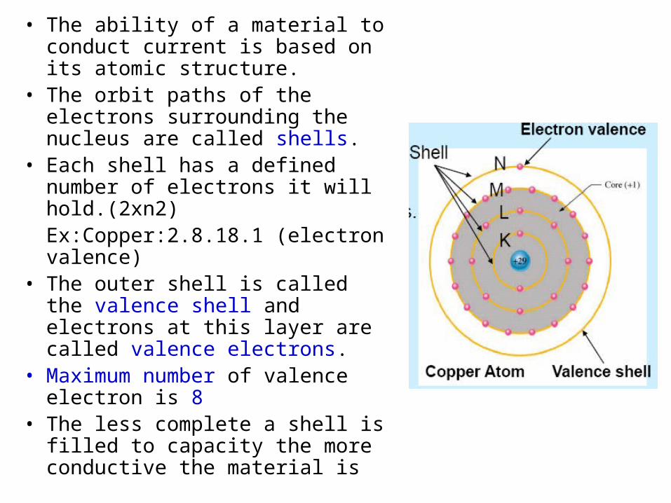
• This creates the depletion region and has a barrier potential
• The depletion region is a region depleted of any charge carriers
• An electric field oriented in the direction from the (+) charge to the (-) charge will be created.
• Built-in Potential Barrier or Built-in Voltage (Vbi) is a potential difference across the depletion region.
• Value of Vbi for Germanium (0.3V) and Silicon (0.7V)

No bias
In the absence of an applied bias voltage, the net flow of charge in any one direction for a p-n junction is zero.

No bias
Note that the arrow is associated with p-type component and the bar with the n-type region. As indicated for VD=0V, the current in any direction is 0 mA.

Reverse Bias condition (VD< 0V)
The p-type material is connected to the negative terminal and the n-type is connected to the positive terminal.

The positive terminal of the battery extracts free electrons from the n-region and the negative terminal extracts free holes (positive ions) from the p-region.The number of uncovered positive ion in the n-region and negative ions in the p-region will increase. Hence, the width of the depletion region increases.

Cont’
However, in real P-N junction, there is a small flow of current in the reversed-biased mode. This is due to the thermally generated electrons and holes which cross the junction to the battery terminals.
As the temperature is high enough, there will be a constant generation of electron-hole pairs and the current exists is called the reverse-saturation current, Is or leakage current.

Forward Bias condition (VD > 0V)
The p-type material is connected to the positive terminal and the n-type is connected to the negative terminal.
Cont’
Positive terminal of the battery will push the holes in the p-region towards the junction.
Hence, the recombination process occurs and the number of negative ion in the p-region near the junction decreases.

Cont’
Negative terminal of the battery will push the free electron in the n-region towards the junction and recombine with the positive ion.
Hence, the number of positive ion decreases. As a result, the number of uncovered ions is reduced and the width of the depletion region will also reduce.

Cont’
Since, the barrier potential is now reduced; electrons in n-type will be easily moved to the p-region.
This is also assisted by the negative terminal which push the electrons and positive terminal that pulls the electron. Hence, a heavy majority carrier flows across the junction

Breakdown Voltage
When a reverse-bias is applied to a p-n junction (diode), the electric field in the depletion region increases.
The electric field may become large enough that covalent bonds are broken and electron hole pairs are created.
Electrons are swept into the n-region and holes are swept into the p-region by the electric field, generating a large reverse current. This phenomenon is called breakdown.
This current can be limited by the external circuit. If this current is not limited, a large Power can be dissipated in the junction that may damage the device and cause burnout.

Review
1. Draw and state the meaning of forward biased voltage and reverse biased voltage supplied across a P-N junction
2. Identify the effects when a P-N junction is supplied with forward biased voltage and reverse biased voltage on the following items a. Area of depletion regionb. Junction resistancec. Current flow
3 Explain why breakdown occurs when P-N junction is reverse biased.

END


![Chapter 1: Qlik Sense Self-Service Model€¦ · Qlik Sense. Graphics Chapter 1 [ 4 ] Graphics Chapter 1 [ 5 ] Graphics Chapter 1 [ 6 ] Graphics Chapter 1 [ 7 ] Chapter 3: Security](https://img.pdfslide.net/doc/110x75/603a754026637d7e176f5238/chapter-1-qlik-sense-self-service-model-qlik-sense-graphics-chapter-1-4-graphics.jpg)


![Chapter 1: Getting Started with Alteryx · Chapter 1 [ 42 ] Chapter 4: Writing Fast and Accurate. Chapter 1 [ 43 ] Chapter 1 [ 44 ]](https://img.pdfslide.net/doc/110x75/5e903c60f316447eb43c0e7a/chapter-1-getting-started-with-alteryx-chapter-1-42-chapter-4-writing-fast.jpg)


![Chapter 01: Relational Databases - static.packt-cdn.com · Chapter 01: Relational Databases. Chapter 1 [ 2 ] Chapter 1 [ 3 ] Chapter 1 [ 4 ] Chapter 1 [ 5 ] Chapter 02: PostgreSQL](https://img.pdfslide.net/doc/110x75/5e1e7793cab1f72f70306c15/chapter-01-relational-databases-chapter-01-relational-databases-chapter-1-.jpg)