Embed Size (px)
Citation preview
EE141
1
System-on-Chip Test Architectures Ch. 10 – Design for Debug and Diagnosis - P. 1
Chapter 10Chapter 10
Design for Debug & Diagnosis Design for Debug & Diagnosis

EE141
2
System-on-Chip Test Architectures Ch. 10 – Design for Debug and Diagnosis - P. 2
What is this chapter about?What is this chapter about?
� Introduce the concept of chip debug and diagnosis and show various design features that are needed for successful debug and diagnosis
� Focus on� design features at the architectural, logic, circuit, and layout
level that are needed to facilitate silicon debug and defect diagnosis of integrated circuits.
� Circuit editing features so that chips can be repaired and hypothesis validated and confirm root cause fixes
� Provide an overview of the debug and diagnosis process (strategy and flow/methodology)

EE141
3
System-on-Chip Test Architectures Ch. 10 – Design for Debug and Diagnosis - P. 3
Design for Debug and DiagnosisDesign for Debug and Diagnosis
� Introduction
� Logic Design for Debug and Diagnosis (DFD)
Structures
� Probing Technologies
� Circuit Editing
� Physical DFD Structures
� Diagnosis and Debug Process
� Summary and Future Challenges
EE141
4
System-on-Chip Test Architectures Ch. 10 – Design for Debug and Diagnosis - P. 4
IntroductionIntroduction
� New chip designs are likely to require debug
before they can go into manufacturing
� Manufacturing startup/ramp also may require
low yield analysis for yield improvement
� Chip in use may fail due to infant mortality or
other failure/wearout mechanism that may
requires investigation
Debugging must be planned for during the design of chips to ease any of these needs
EE141
5
System-on-Chip Test Architectures Ch. 10 – Design for Debug and Diagnosis - P. 5
Debug vs. DiagnosisDebug vs. Diagnosis
� Diagnosis: investigation or analysis of the cause or nature of a condition, situation, or problem
� Debug: the process of isolating bugs or errors that causes a design to behave differently from its intended behavior under its specified operating conditions.
� To answer: � What was wrong with this device?
� Which chip was bad on this board?
� Why did this system crash?
� Why did the simulation of the arithmetic logic unit (ALU) show that 2+2=5?
� Why was this signal late?
EE141
6
System-on-Chip Test Architectures Ch. 10 – Design for Debug and Diagnosis - P. 6
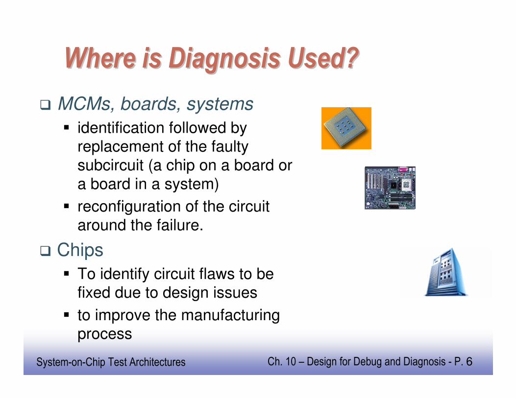
Where is Diagnosis Used?Where is Diagnosis Used?
� MCMs, boards, systems
� identification followed by replacement of the faulty
subcircuit (a chip on a board or
a board in a system)
� reconfiguration of the circuit
around the failure.
� Chips
� To identify circuit flaws to be fixed due to design issues
� to improve the manufacturing process
EE141
7
System-on-Chip Test Architectures Ch. 10 – Design for Debug and Diagnosis - P. 7
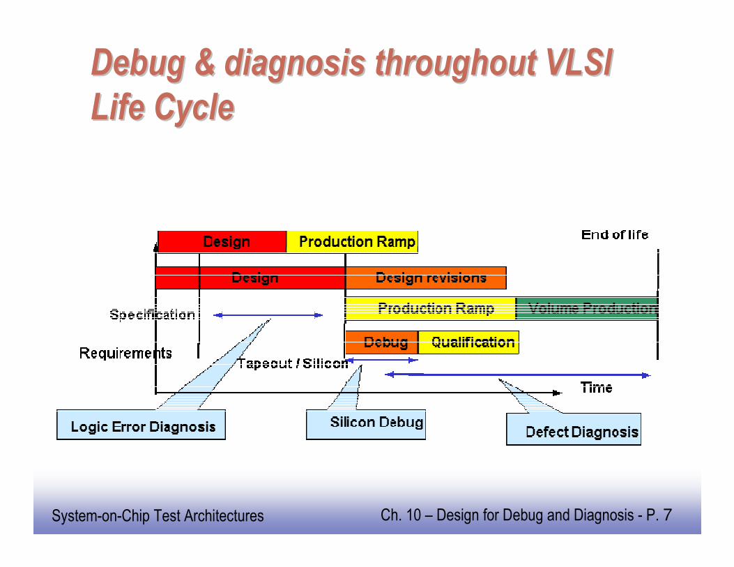
Debug & diagnosis throughout VLSI Debug & diagnosis throughout VLSI
Life CycleLife Cycle
EE141
8
System-on-Chip Test Architectures Ch. 10 – Design for Debug and Diagnosis - P. 8
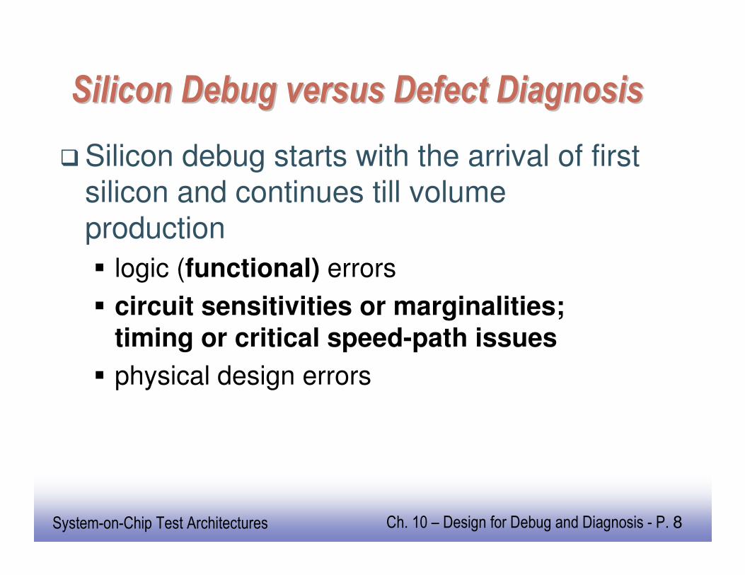
Silicon Debug versus Defect DiagnosisSilicon Debug versus Defect Diagnosis
� Silicon debug starts with the arrival of first silicon and continues till volume production
� logic (functional) errors
� circuit sensitivities or marginalities;
timing or critical speed-path issues
� physical design errors
EE141
9
System-on-Chip Test Architectures Ch. 10 – Design for Debug and Diagnosis - P. 9
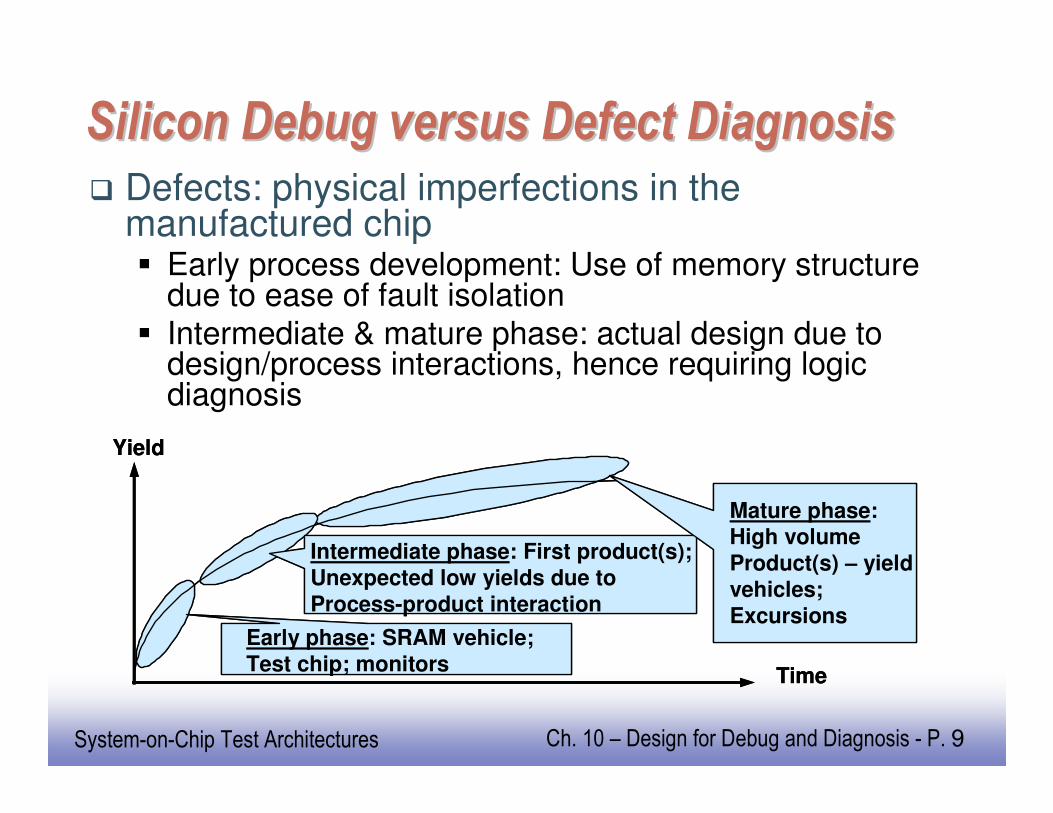
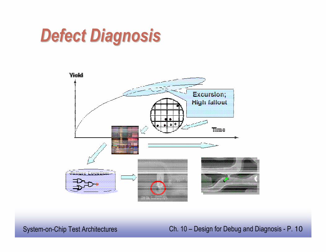
Silicon Debug versus Defect DiagnosisSilicon Debug versus Defect Diagnosis� Defects: physical imperfections in the
manufactured chip� Early process development: Use of memory structure
due to ease of fault isolation
� Intermediate & mature phase: actual design due to design/process interactions, hence requiring logic diagnosis
Time
Yield
Early phase: SRAM vehicle;
Test chip; monitors
Intermediate phase: First product(s);
Unexpected low yields due to
Process-product interaction
Mature phase: High volume
Product(s) – yield
vehicles;
Excursions
Time
Yield
Early phase: SRAM vehicle;
Test chip; monitors
Intermediate phase: First product(s);
Unexpected low yields due to
Process-product interaction
Mature phase: High volume
Product(s) – yield
vehicles;
Excursions
EE141
10
System-on-Chip Test Architectures Ch. 10 – Design for Debug and Diagnosis - P. 10
Defect DiagnosisDefect Diagnosis
EE141
11
System-on-Chip Test Architectures Ch. 10 – Design for Debug and Diagnosis - P. 11
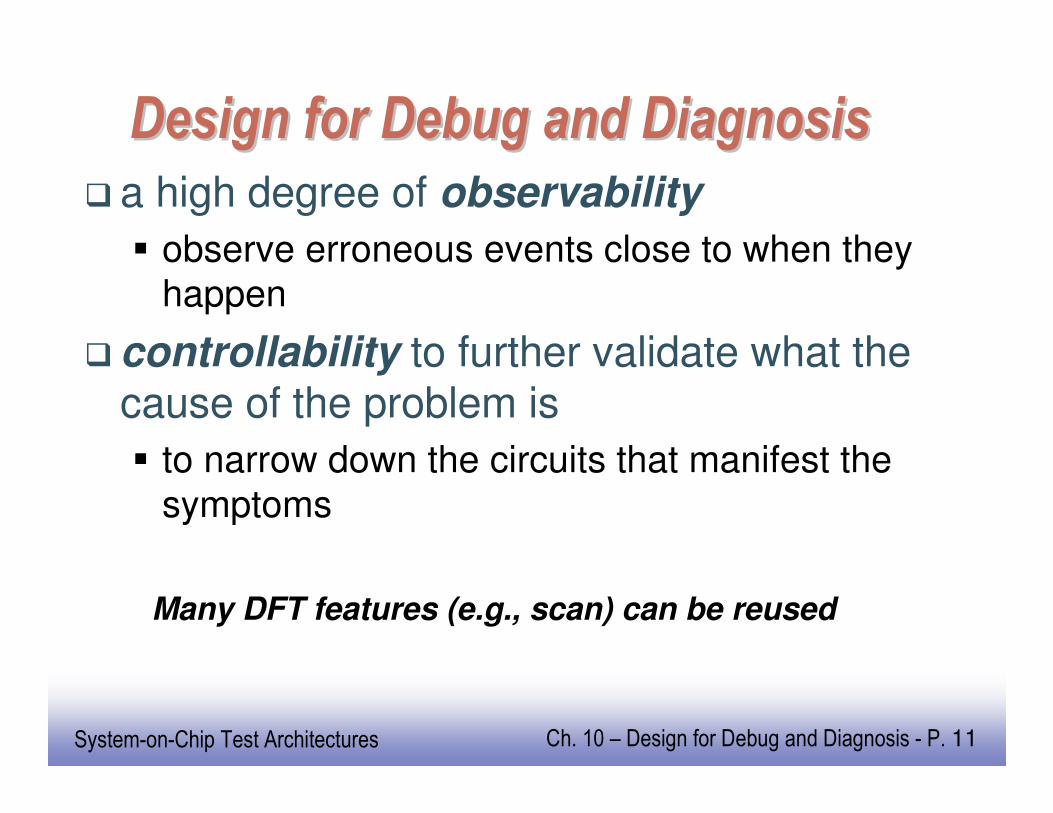
Design for Debug and DiagnosisDesign for Debug and Diagnosis� a high degree of observability
� observe erroneous events close to when they
happen
� controllability to further validate what the cause of the problem is
� to narrow down the circuits that manifest the
symptoms
Many DFT features (e.g., scan) can be reused
EE141
12
System-on-Chip Test Architectures Ch. 10 – Design for Debug and Diagnosis - P. 12
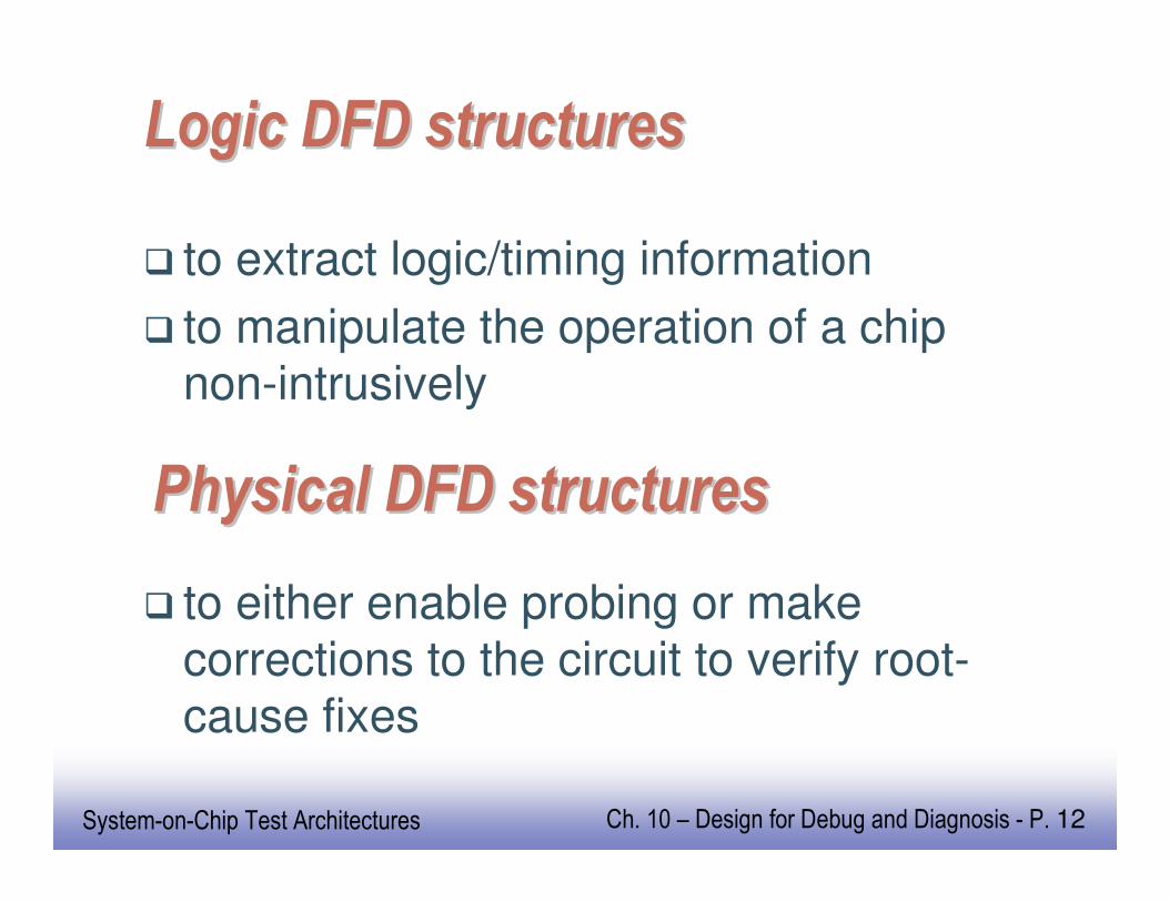
Logic DFD structuresLogic DFD structures
� to extract logic/timing information
� to manipulate the operation of a chip non-intrusively
Physical DFD structuresPhysical DFD structures
� to either enable probing or make corrections to the circuit to verify root-cause fixes
EE141
13
System-on-Chip Test Architectures Ch. 10 – Design for Debug and Diagnosis - P. 13
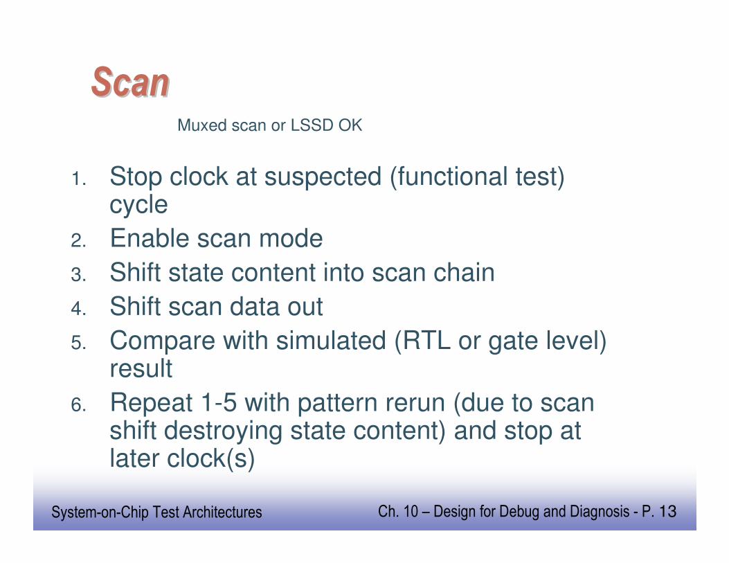
ScanScan
1. Stop clock at suspected (functional test) cycle
2. Enable scan mode
3. Shift state content into scan chain
4. Shift scan data out
5. Compare with simulated (RTL or gate level) result
6. Repeat 1-5 with pattern rerun (due to scan shift destroying state content) and stop at later clock(s)
Muxed scan or LSSD OK
EE141
14
System-on-Chip Test Architectures Ch. 10 – Design for Debug and Diagnosis - P. 14
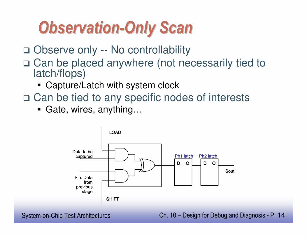
ObservationObservation--Only ScanOnly Scan
� Observe only -- No controllability
� Can be placed anywhere (not necessarily tied to latch/flops)� Capture/Latch with system clock
� Can be tied to any specific nodes of interests� Gate, wires, anything…
Data to be captured
SHIFT
LOAD
D O
Sout
Ph1 latch
D O
Ph2 latch
Sin: Data from
previous stage
Data to be captured
SHIFT
LOAD
D OD O
Sout
Ph1 latch
D OD O
Ph2 latch
Sin: Data from
previous stage
EE141
15
System-on-Chip Test Architectures Ch. 10 – Design for Debug and Diagnosis - P. 15
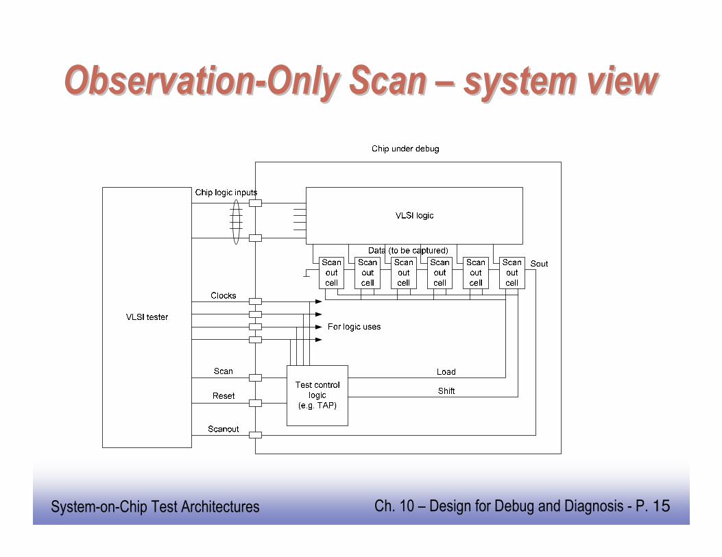
ObservationObservation--Only Scan Only Scan –– system viewsystem view

EE141
16
System-on-Chip Test Architectures Ch. 10 – Design for Debug and Diagnosis - P. 16
Observation Points with MultiplexersObservation Points with Multiplexers
� multiplexers to concatenate individual signals to be mapped out to a test port
� Programmable interface may allow different sets of signals to be observed at different times
� Logically simple, BUT� Test/Mux control may be
massive
� Not routing friendly
� Signals you needed may not be included
EE141
17
System-on-Chip Test Architectures Ch. 10 – Design for Debug and Diagnosis - P. 17
Array Dump and Trace Logic AnalyzerArray Dump and Trace Logic Analyzer
� Array structures are usually not scanned� Need array dump feature
� Content unloaded onto convenient output interfaces (e.g. buses or TDO)
� Reversed feature (array load) may be desirable for validation of hypothesis
� Arrays can be deployed for storing on-chip events� Bus transactions, various signals
� Aka on-chip Logic Analyzer
� Original array resized for original purposes
EE141
18
System-on-Chip Test Architectures Ch. 10 – Design for Debug and Diagnosis - P. 18
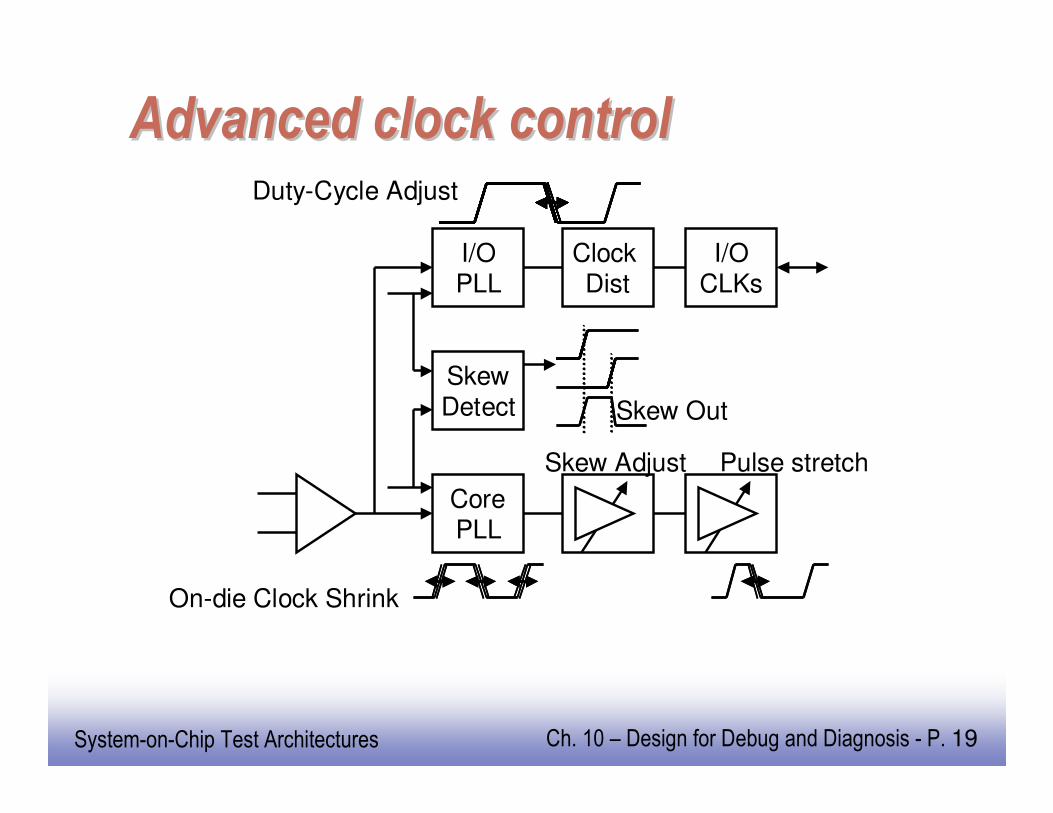
Clock controlClock control� “Where” from scan/scanout
� “When” with clock control
� Starting, stopping, and restarting of internal clocks while keeping them synchronized to specific external and internal events � Clock is internally synthesized from PLL
� Offset counters – E.g. 487 clock cycles after an exception event
� Single stepping
� Clock stop + scan dump
EE141
19
System-on-Chip Test Architectures Ch. 10 – Design for Debug and Diagnosis - P. 19
Advanced clock controlAdvanced clock control
CorePLL
I/OPLL
Clock Dist
I/OCLKs
Pulse stretchSkew Adjust
On-die Clock Shrink
Duty-Cycle Adjust
SkewDetect Skew Out

EE141
20
System-on-Chip Test Architectures Ch. 10 – Design for Debug and Diagnosis - P. 20
Advanced clock controlAdvanced clock control

EE141
21
System-on-Chip Test Architectures Ch. 10 – Design for Debug and Diagnosis - P. 21
Partitioning, Isolation, and DePartitioning, Isolation, and De--featuringfeaturing
� Partitioning: separate/decouple blocks� Does problem still exist?
� E.g. disabling the caches
� Isolation/defeaturing: selective disabling of features to allow identification of specific area� E.g. turns off different execution units in
turns
� Restricted to logic blocks that are not absolutely needed

EE141
22
System-on-Chip Test Architectures Ch. 10 – Design for Debug and Diagnosis - P. 22
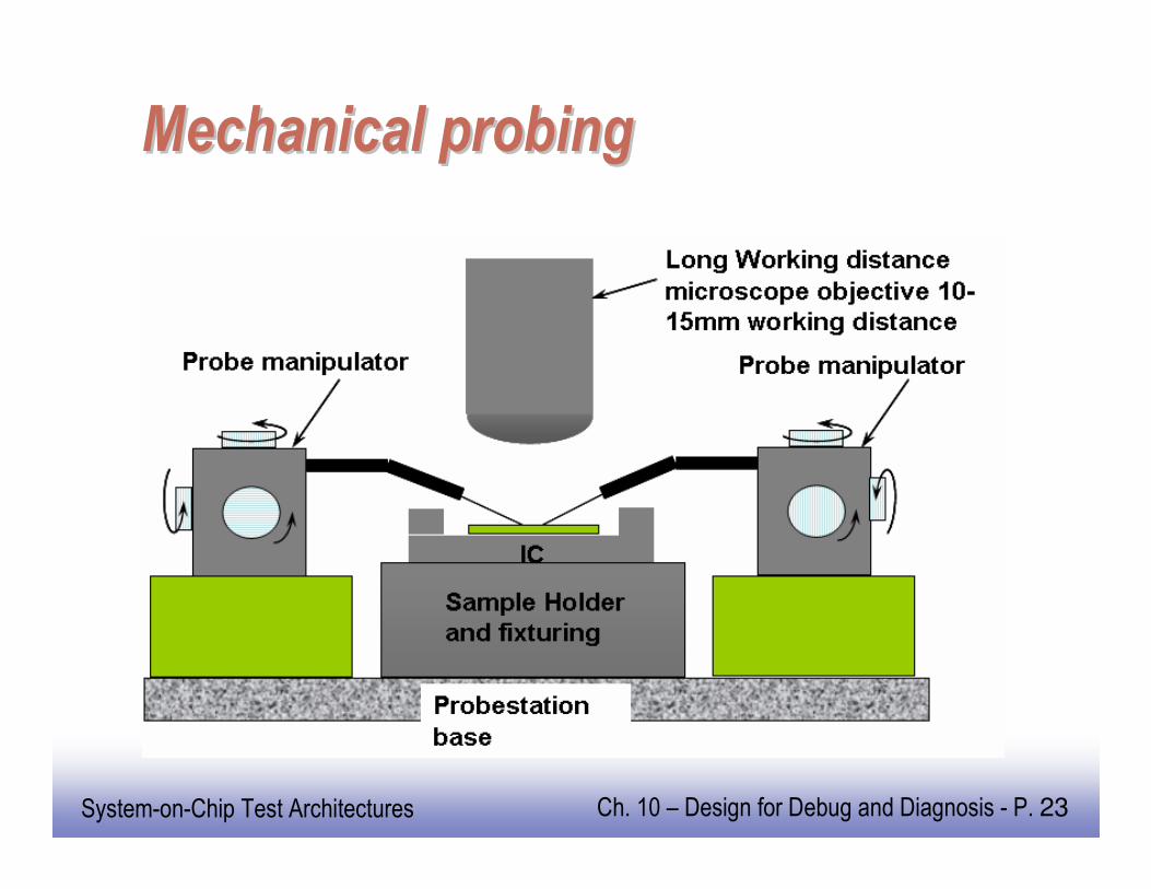
Probing TechnologiesProbing Technologies
� Contact probing� Mechanical probing
� Non-contact probing� Beam injection (laser or e-beam)
� Emission detection (photon or thermal infrared)
EE141
23
System-on-Chip Test Architectures Ch. 10 – Design for Debug and Diagnosis - P. 23
Mechanical probingMechanical probing
EE141
24
System-on-Chip Test Architectures Ch. 10 – Design for Debug and Diagnosis - P. 24
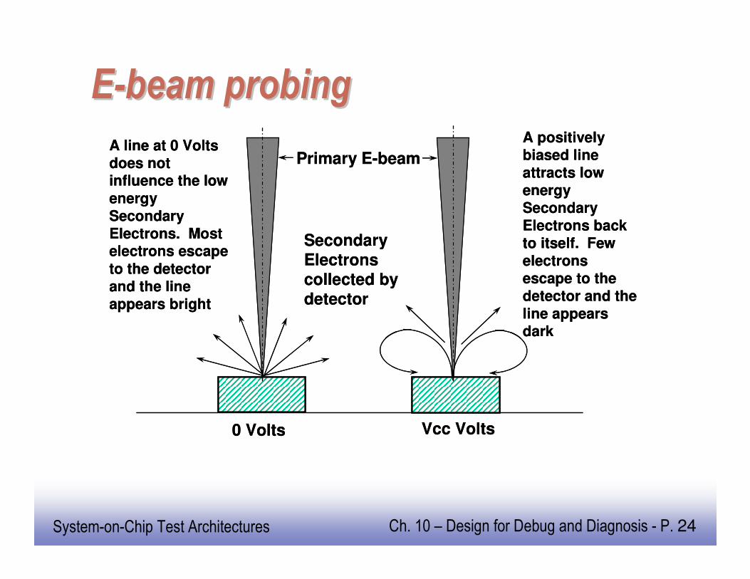
EE--beam probingbeam probing
0 Volts Vcc Volts
Primary E-beam
Secondary Electrons collected by detector
A positively
biased line
attracts low
energy
Secondary
Electrons back
to itself. Few
electrons
escape to the
detector and the
line appears
dark
A line at 0 Volts
does not influence the low
energy
Secondary
Electrons. Most electrons escape
to the detector
and the line
appears bright
EE141
25
System-on-Chip Test Architectures Ch. 10 – Design for Debug and Diagnosis - P. 25
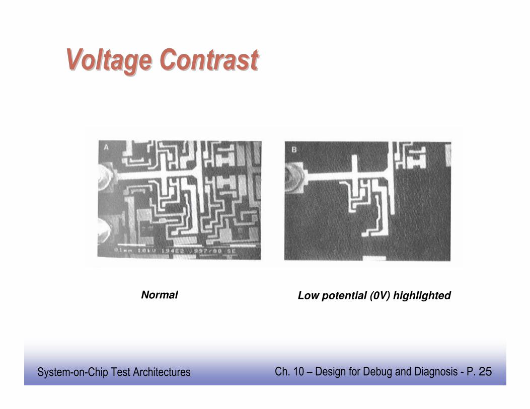
Voltage ContrastVoltage Contrast
Normal Low potential (0V) highlighted
EE141
26
System-on-Chip Test Architectures Ch. 10 – Design for Debug and Diagnosis - P. 26
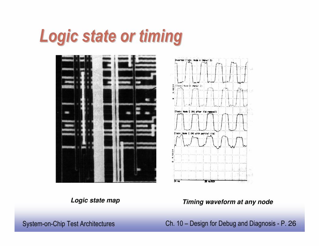
Logic state or timingLogic state or timing
Logic state map Timing waveform at any node
EE141
27
System-on-Chip Test Architectures Ch. 10 – Design for Debug and Diagnosis - P. 27
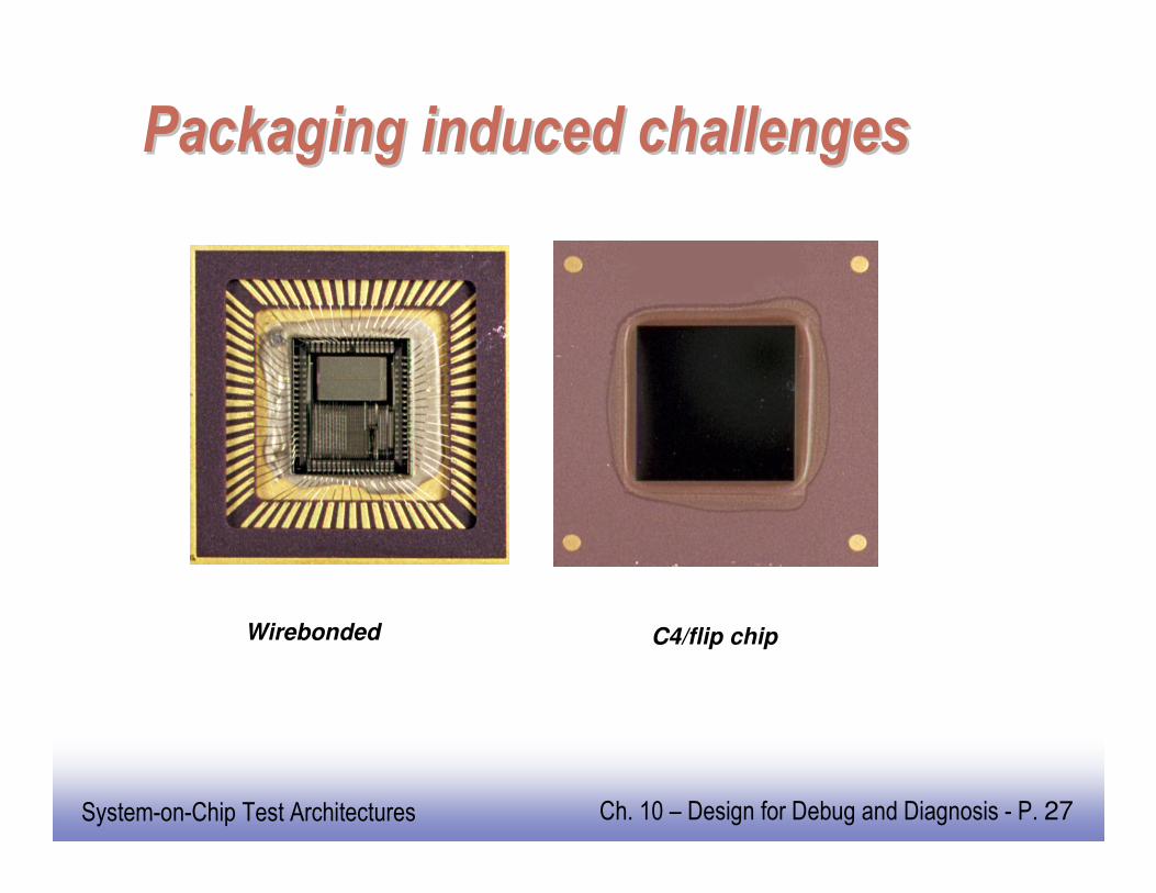
Packaging induced challengesPackaging induced challenges
Wirebonded C4/flip chip
EE141
28
System-on-Chip Test Architectures Ch. 10 – Design for Debug and Diagnosis - P. 28
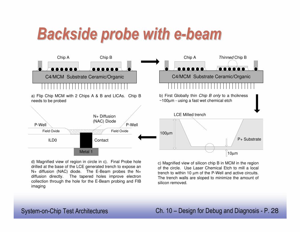
Backside probe with eBackside probe with e--beambeam
C4/MCM Substrate Ceramic/Organic C4/MCM Substrate Ceramic/Organic
a) Flip Chip MCM with 2 Chips A & B and LICAs. Chip B
needs to be probed
Chip A Chip B
b) First Globally thin Chip B only to a thcikness
~100µm - using a fast wet chemical etch
Chip A Thinned Chip B
Metal 1
c) Magnified view of silicon chip B in MCM in the region
of the circle. Use Laser Chemical Etch to mill a local
trench to within 10 µm of the P-Well and active circuits.
The trench walls are sloped to minimize the amount of
silicon removed.
Contact
Field Oxide
d) Magnified view of region in circle in c). Final Probe hole
drilled at the base of the LCE generated trench to expose an N+ diffusion (NAC) diode. The E-Beam probes the N+
diffusion directly. The tapered holes improve electron
collection through the hole for the E-Beam probing and FIB imaging
ILD0
Field Oxide
P-Well P-Well
100µm
10µm
N+ Diffusion
(NAC) Diode
P+ Substrate
LCE Milled trench

EE141
29
System-on-Chip Test Architectures Ch. 10 – Design for Debug and Diagnosis - P. 29
Optical probingOptical probing
Front view (metal blocking much
of the area underneath)
Backside view using IR
Silicon is transparent to IR

EE141
30
System-on-Chip Test Architectures Ch. 10 – Design for Debug and Diagnosis - P. 30
Optical probing principleOptical probing principle
N+
p-well
ILD0Metal
Incident IR
BeamReflected IR Beam
time
Op
tica
l
po
we
r
With NO input
electrical signal
Reflected optical power
Input
electrical signal
E(t)
High
electric field region
time
Op
tic
al
po
wer
With applied
electrical signal
N+
p-well
ILD0Metal
N+
p-well
ILD0Metal
Incident IR
Beam
Incident IR
BeamReflected IR BeamReflected IR Beam
time
Op
tica
l
po
we
r
With NO input
electrical signal
Reflected optical power
time
Op
tica
l
po
we
r
With NO input
electrical signal
Reflected optical power
Input
electrical signal
E(t)
Input
electrical signal
E(t)E(t)
High
electric field region
High
electric field region
time
Op
tic
al
po
wer
With applied
electrical signal
time
Op
tic
al
po
wer
With applied
electrical signal
EE141
31
System-on-Chip Test Architectures Ch. 10 – Design for Debug and Diagnosis - P. 31
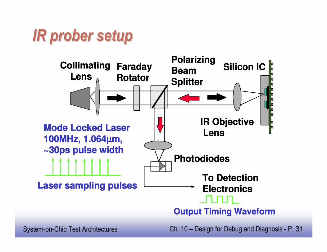
IR IR proberprober setupsetup
Mode Locked Laser
100MHz, 1.064µµµµm, ~30ps pulse width
Laser sampling pulses
Silicon ICCollimating Lens
Faraday Rotator
IR ObjectiveLens
Polarizing Beam Splitter
Photodiodes
To Detection Electronics
Output Timing Waveform
Mode Locked Laser
100MHz, 1.064µµµµm, ~30ps pulse width
Laser sampling pulses
Mode Locked Laser
100MHz, 1.064µµµµm, ~30ps pulse width
Laser sampling pulses
Silicon ICSilicon ICCollimating Lens
Faraday Rotator
IR ObjectiveLens
Polarizing Beam Splitter
Collimating Lens
Faraday Rotator
IR ObjectiveLens
Polarizing Beam Splitter
PhotodiodesPhotodiodes
To Detection ElectronicsTo Detection Electronics
Output Timing WaveformOutput Timing Waveform
EE141
32
System-on-Chip Test Architectures Ch. 10 – Design for Debug and Diagnosis - P. 32
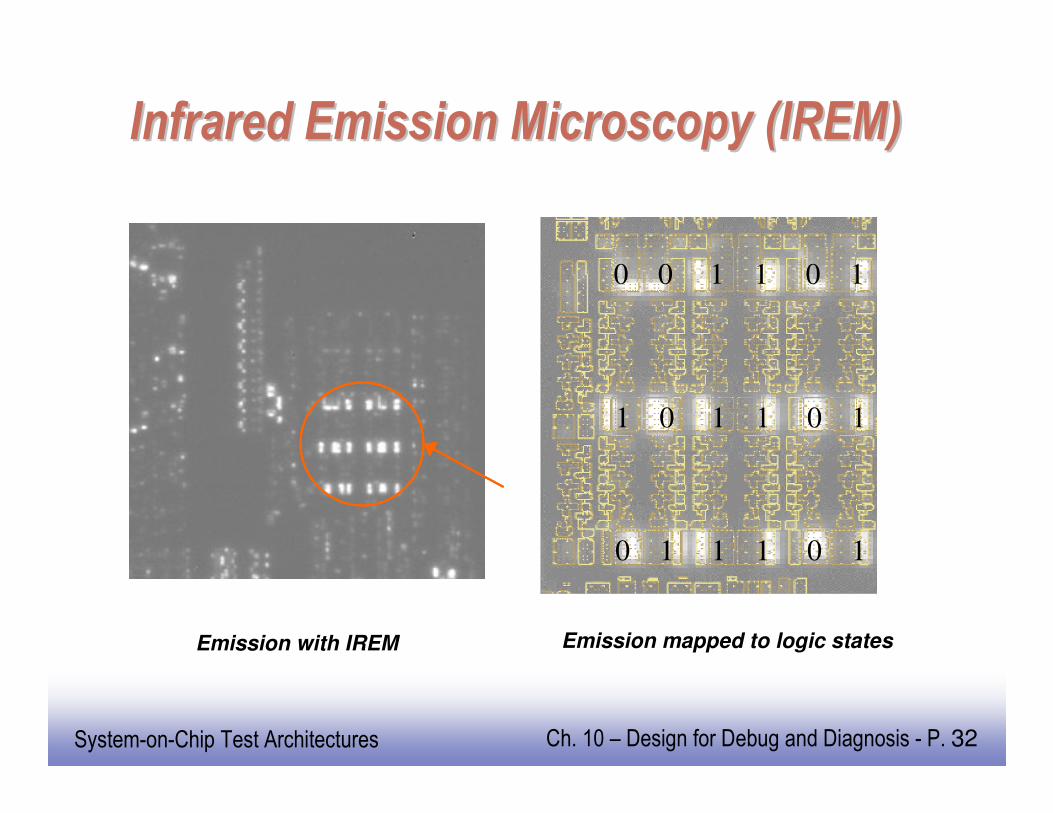
Infrared Emission Microscopy (IREM)Infrared Emission Microscopy (IREM)
0 0 1 1 0 1
1 0 1 1 0 1
0 1 1 1 0 1
0 0 1 1 0 1
1 0 1 1 0 1
0 1 1 1 0 1
Emission mapped to logic statesEmission with IREM
EE141
33
System-on-Chip Test Architectures Ch. 10 – Design for Debug and Diagnosis - P. 33
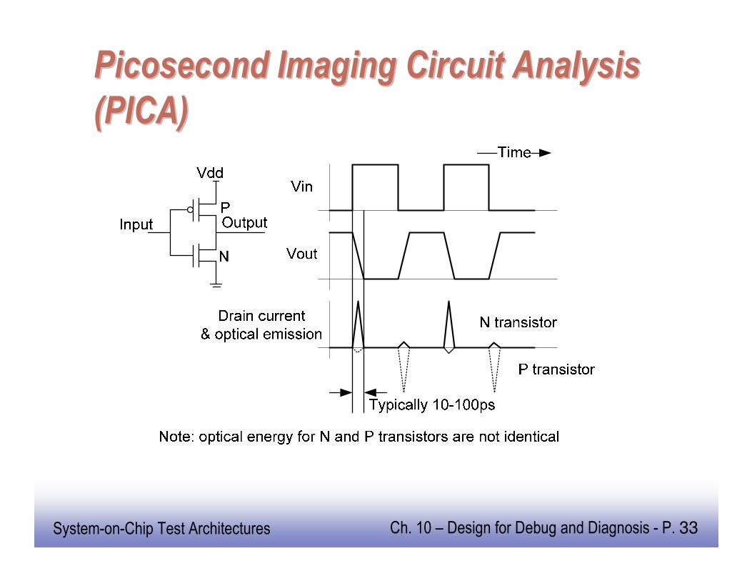
PicosecondPicosecond Imaging Circuit Analysis Imaging Circuit Analysis
(PICA)(PICA)
EE141
34
System-on-Chip Test Architectures Ch. 10 – Design for Debug and Diagnosis - P. 34
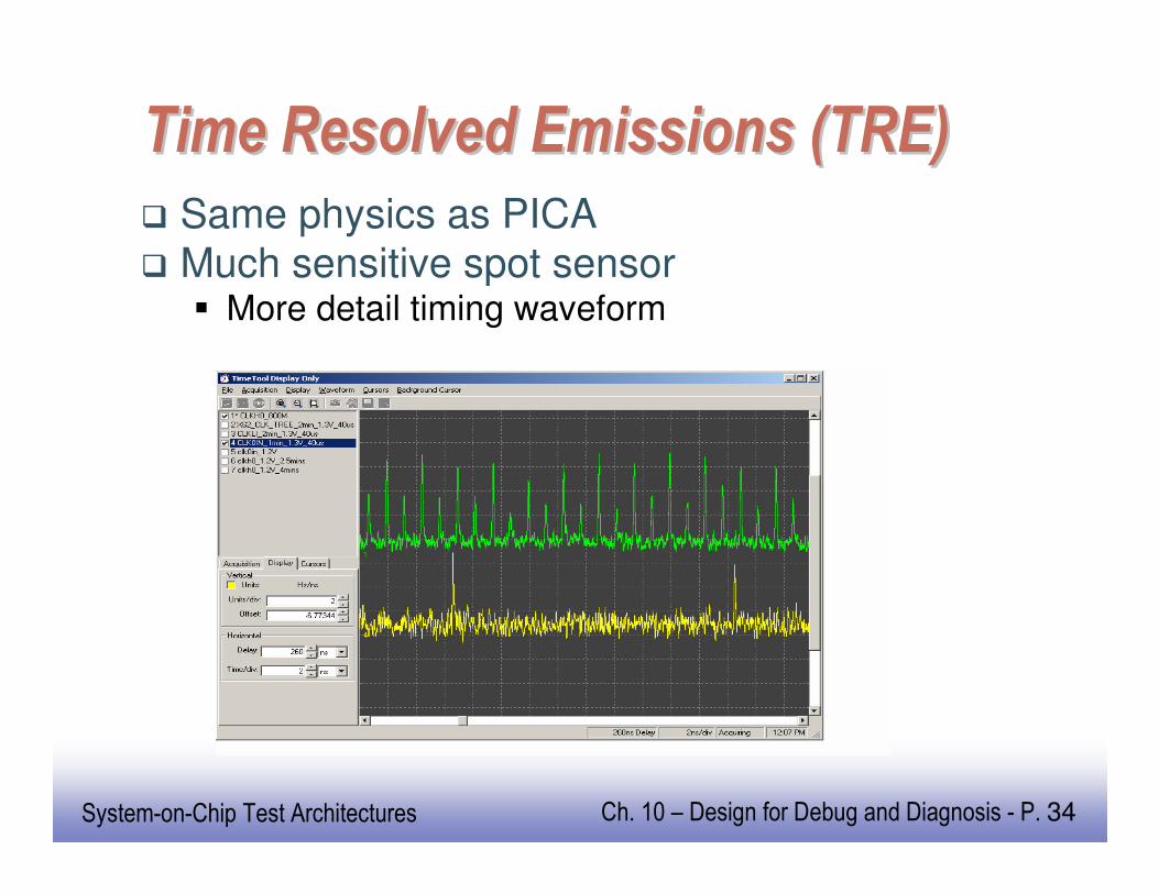
Time Resolved Emissions (TRE) Time Resolved Emissions (TRE)
� Same physics as PICA
� Much sensitive spot sensor� More detail timing waveform
EE141
35
System-on-Chip Test Architectures Ch. 10 – Design for Debug and Diagnosis - P. 35
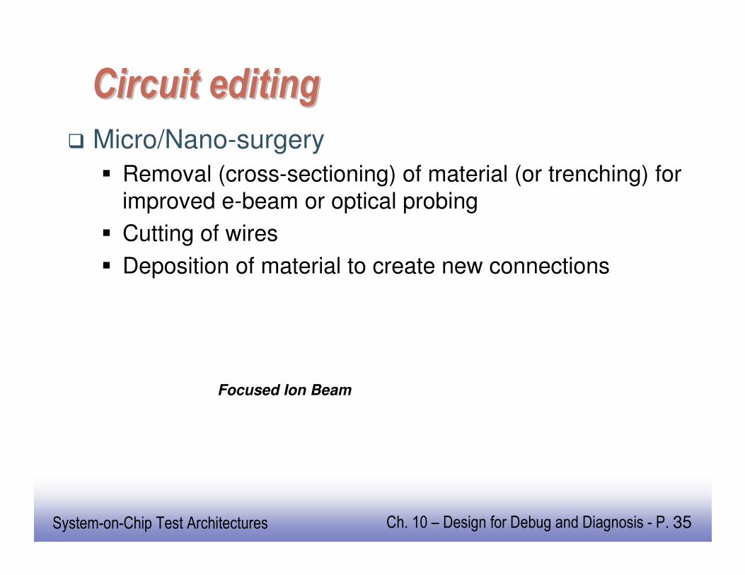
Circuit editingCircuit editing
� Micro/Nano-surgery
� Removal (cross-sectioning) of material (or trenching) for
improved e-beam or optical probing
� Cutting of wires
� Deposition of material to create new connections
Focused Ion Beam

EE141
36
System-on-Chip Test Architectures Ch. 10 – Design for Debug and Diagnosis - P. 36
Focused Ion BeamFocused Ion Beam
EE141
37
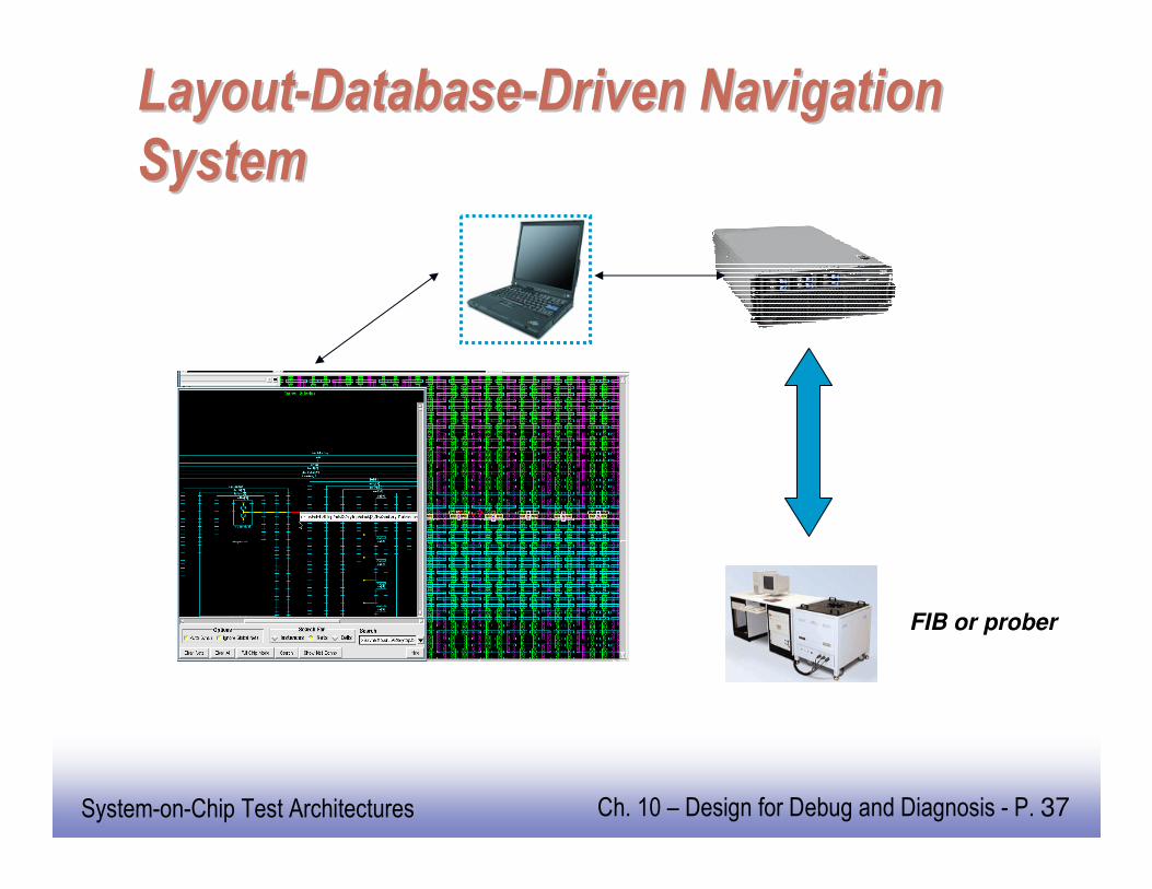
System-on-Chip Test Architectures Ch. 10 – Design for Debug and Diagnosis - P. 37
LayoutLayout--DatabaseDatabase--Driven Navigation Driven Navigation
SystemSystem
FIB or prober

EE141
38
System-on-Chip Test Architectures Ch. 10 – Design for Debug and Diagnosis - P. 38
Linking polygons to schematics to Linking polygons to schematics to
RTLRTL
RTL CodeRTL CodeSilicon DataSilicon Data SchematicsSchematics RTL CodeRTL CodeSilicon DataSilicon Data SchematicsSchematics
EE141
39
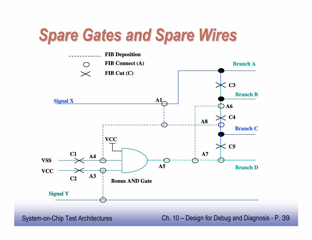
System-on-Chip Test Architectures Ch. 10 – Design for Debug and Diagnosis - P. 39
Spare Gates and Spare Wires Spare Gates and Spare Wires
Branch B
Branch C
Branch D
Bonus AND Gate
Signal Y
Signal X
FIB Deposition
FIB Connect (A)
FIB Cut (C)
VCC
VSS
VCCA3
A4
A5
A7
A1
C1
C2
C3
C5
C4
A6
A8
Branch A
Branch B
Branch C
Branch D
Bonus AND Gate
Signal Y
Signal X
FIB Deposition
FIB Connect (A)
FIB Cut (C)
VCC
VSS
VCCA3
A4
A5
A7
A1
C1
C2
C3
C5
C4
A6
A8
Branch A
EE141
40
System-on-Chip Test Architectures Ch. 10 – Design for Debug and Diagnosis - P. 40
Physical DFDPhysical DFD
� Layout design to facilitate the probing (contact or non-contact; emission or injection probing)
� Layout design is also needed to put in spare gates and spare wires and plans for patching/blue-wiring

EE141
41
System-on-Chip Test Architectures Ch. 10 – Design for Debug and Diagnosis - P. 41
Physical DFD for PicoPhysical DFD for Pico--Probing Probing
� Placement of pads with plenty of open space� Avoid shorting to neighboring wires
� Pads size compatible with probe tip sizes
� Avoid putting active signals underneath probe pads
� Dummy metals may be put underneath for planarization

EE141
42
System-on-Chip Test Architectures Ch. 10 – Design for Debug and Diagnosis - P. 42
Physical Physical
DFD for DFD for
EE--Beam Beam

EE141
43
System-on-Chip Test Architectures Ch. 10 – Design for Debug and Diagnosis - P. 43
Physical DFD for FIB and Probing Physical DFD for FIB and Probing
� Driven by FIB
precision
� Generous spacing
planned for
cutpoints
� Specifically design
cut sites
� Add probe diodes as
probe points
+
+
+
+
+ +
+ +
Package
Silicon(face down)
Package
Fiducials
ChipFiducials
on M1
EE141
44
System-on-Chip Test Architectures Ch. 10 – Design for Debug and Diagnosis - P. 44
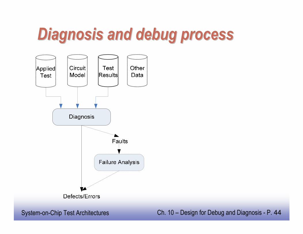
Diagnosis and debug processDiagnosis and debug process

EE141
45
System-on-Chip Test Architectures Ch. 10 – Design for Debug and Diagnosis - P. 45
Fault propagationFault propagation

EE141
46
System-on-Chip Test Architectures Ch. 10 – Design for Debug and Diagnosis - P. 46
Future challengesFuture challenges
� Voltage scaling
� Reliability driven (power also reduced)
� Devices may not be driven to saturation
� Emission reduced
� Smaller charge at any nodes
� Heisenberg Uncertainty Principleapplies – the very act of observing something changes its nature
EE141
47
System-on-Chip Test Architectures Ch. 10 – Design for Debug and Diagnosis - P. 47
Future ChallengesFuture Challenges
� Dynamic and leakage power
� Thermal density & heat removal during debug
� Adaptive control of voltage & frequency
� How to debug under these dynamic situations?
� On-chip DFD to supplement inadequacy of
ATE
� Tools to help with identification of sensitive
circuits, DFD implementations, test
generation for debug, debug automation

EE141
48
System-on-Chip Test Architectures Ch. 10 – Design for Debug and Diagnosis - P. 48
SummarySummary� This chapter presented an
overview of the debug/diagnosis process, logical/timing debug, various probing technologies as well as circuit editing technologies
� Provided unique guidance for logical and physical design for debug
� Future challenges are identified for audience to pursue
![team project #1 Digital Watch SAdslab.konkuk.ac.kr/Class/2019/19SE/TEAM_B/p1/[T7]SRA_ppt.pdfSystem Context Diagram DFD Level 0 DFD Level 1 DFD Level 2 DFD Level 3 DFD Level 4 DFD DFD](https://img.pdfslide.net/doc/110x75/5e279d2cd253ad54536a6e3a/team-project-1-digital-watch-t7srapptpdf-system-context-diagram-dfd-level-0.jpg)