Embed Size (px)
Citation preview
CHAPTER 15 BASIC DIGITAL CONCEPTS, LOGIC GATES 15-1
Chapter 15 BASIC DIGITAL CONCEPTS and LOGIC GATES What are digital signals? So far, we have generally dealt with current or voltage signals which have a continuous range of possible values. For example, a voltage might be 2.1392 volts, or 2.1393 volts, or in fact any value in between. Most quantities which are not actually counted (i.e. they have non-integer values) are like this, and are referred to as analog1 signals. As you have seen, analog signals can be degraded, for example, by the addition of noise, so that the full amount of information originally contained in them cannot be recovered. Digital signals, on the other hand, can have only a certain number of possible values, and for the basic logic circuits that we will be discussing shortly, there are only two possible values. In reality, a digital signal must still be represented by an analog voltage, which of course may be corrupted by noise and so on. Having two possible values then might work something like this, allowing for noise: let’s suppose the two possible values for a voltage are zero and 1 volt. Then, if the voltage is less than 0.5 volts, assume its actual value is zero volts; if it is greater than 0.5 volts, assume it’s actually 1 volt. You might see that this could have some advantages. Some are: • If the signal is supposed to be zero volts, it needs a lot of noise to make
it appear as 1 volt, and vice versa. That is, the S/N ratio would have to be very poor for an error to occur. Although the digital signal doesn’t contain much information, it’s pretty robust.
• The circuits which use signals like these don’t need to be nice and linear. In fact, it’s actually best if they aren’t, but tend to “stick” to voltage values of (in this example) zero or 1 volt.
Representing information in binary form A “two-state” signal like this is called a binary signal, and can be used to represent any information which also has two possible states. These might be, for example: • True/false • High/low • Yes/no • 1/0
1 The alternative spelling of analog is analogue. The former tends to be American usage, the latter British.
CHAPTER 15 BASIC DIGITAL CONCEPTS, LOGIC GATES 15-2
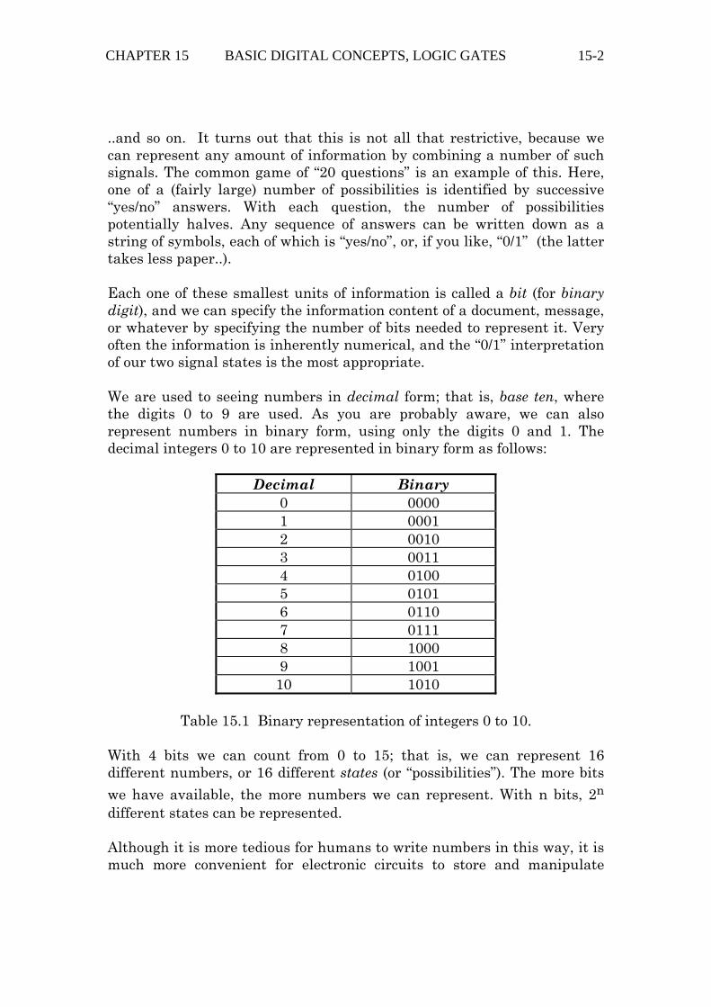
..and so on. It turns out that this is not all that restrictive, because we can represent any amount of information by combining a number of such signals. The common game of “20 questions” is an example of this. Here, one of a (fairly large) number of possibilities is identified by successive “yes/no” answers. With each question, the number of possibilities potentially halves. Any sequence of answers can be written down as a string of symbols, each of which is “yes/no”, or, if you like, “0/1” (the latter takes less paper..). Each one of these smallest units of information is called a bit (for binary digit), and we can specify the information content of a document, message, or whatever by specifying the number of bits needed to represent it. Very often the information is inherently numerical, and the “0/1” interpretation of our two signal states is the most appropriate. We are used to seeing numbers in decimal form; that is, base ten, where the digits 0 to 9 are used. As you are probably aware, we can also represent numbers in binary form, using only the digits 0 and 1. The decimal integers 0 to 10 are represented in binary form as follows:
Decimal Binary 0 0000 1 0001 2 0010 3 0011 4 0100 5 0101 6 0110 7 0111 8 1000 9 1001
10 1010
Table 15.1 Binary representation of integers 0 to 10. With 4 bits we can count from 0 to 15; that is, we can represent 16 different numbers, or 16 different states (or “possibilities”). The more bits
we have available, the more numbers we can represent. With n bits, 2n different states can be represented. Although it is more tedious for humans to write numbers in this way, it is much more convenient for electronic circuits to store and manipulate
CHAPTER 15 BASIC DIGITAL CONCEPTS, LOGIC GATES 15-3
them, and the binary representation is used in computers. Most personal computers these days basically represent numbers using 32 or 64 bits. This is referred to as the word length of the computer. With 32 bits, we
can count from 0 to 4,294,967,295 ( = 232 or 4,294,967,296 possible states). The table below shows the number of possible states for some common word lengths encountered in digital circuits or computers. Note that a byte is a group of 8 bits.
Word length in bits Possible number of states 4 16 8 (1 byte) 256 16 (2 bytes) 65,536 32 (4 bytes) 4,294,967,296 64 (8 bytes) 18,446,744,073,709,551,616
Table 15.2 Number of states (or different numbers, or other possibilities)
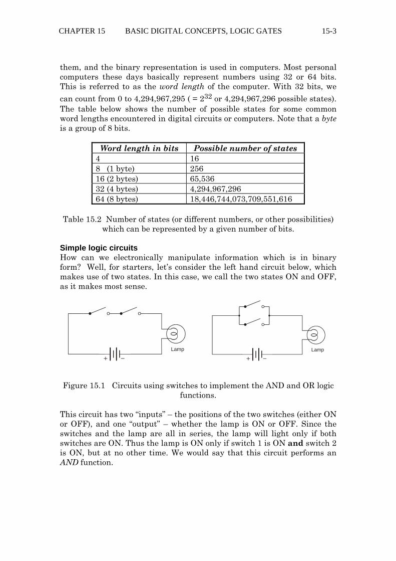
which can be represented by a given number of bits. Simple logic circuits How can we electronically manipulate information which is in binary form? Well, for starters, let’s consider the left hand circuit below, which makes use of two states. In this case, we call the two states ON and OFF, as it makes most sense.
Lamp
Lamp
Figure 15.1 Circuits using switches to implement the AND and OR logic functions.
This circuit has two “inputs” – the positions of the two switches (either ON or OFF), and one “output” – whether the lamp is ON or OFF. Since the switches and the lamp are all in series, the lamp will light only if both switches are ON. Thus the lamp is ON only if switch 1 is ON and switch 2 is ON, but at no other time. We would say that this circuit performs an AND function.
CHAPTER 15 BASIC DIGITAL CONCEPTS, LOGIC GATES 15-4
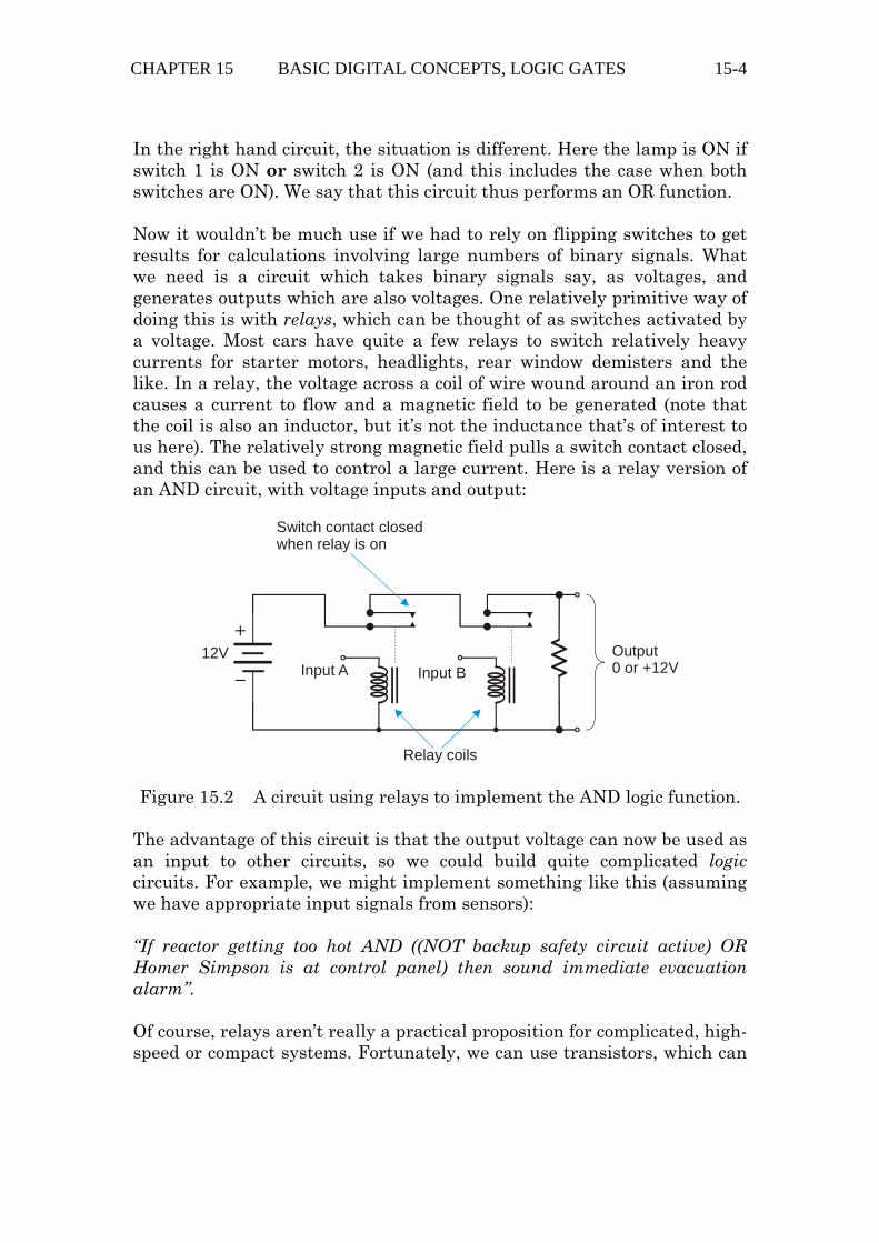
In the right hand circuit, the situation is different. Here the lamp is ON if switch 1 is ON or switch 2 is ON (and this includes the case when both switches are ON). We say that this circuit thus performs an OR function. Now it wouldn’t be much use if we had to rely on flipping switches to get results for calculations involving large numbers of binary signals. What we need is a circuit which takes binary signals say, as voltages, and generates outputs which are also voltages. One relatively primitive way of doing this is with relays, which can be thought of as switches activated by a voltage. Most cars have quite a few relays to switch relatively heavy currents for starter motors, headlights, rear window demisters and the like. In a relay, the voltage across a coil of wire wound around an iron rod causes a current to flow and a magnetic field to be generated (note that the coil is also an inductor, but it’s not the inductance that’s of interest to us here). The relatively strong magnetic field pulls a switch contact closed, and this can be used to control a large current. Here is a relay version of an AND circuit, with voltage inputs and output:
12VInput A Input B
Output0 or +12V
Switch contact closedwhen relay is on
Relay coils
Figure 15.2 A circuit using relays to implement the AND logic function. The advantage of this circuit is that the output voltage can now be used as an input to other circuits, so we could build quite complicated logic circuits. For example, we might implement something like this (assuming we have appropriate input signals from sensors): “If reactor getting too hot AND ((NOT backup safety circuit active) OR Homer Simpson is at control panel) then sound immediate evacuation alarm”. Of course, relays aren’t really a practical proposition for complicated, high-speed or compact systems. Fortunately, we can use transistors, which can
CHAPTER 15 BASIC DIGITAL CONCEPTS, LOGIC GATES 15-5
be coaxed to act in a somewhat similar way to relays, to build fast, cheap, compact and incredibly reliable logic circuits. It is now commonplace to buy integrated circuits (ICs, or “silicon chips”) containing millions of such circuits. The integrated circuits inside your computer are exactly like this, made up of a large number of very basic building blocks. Just as in the case of amplifiers, we won’t be looking at how transistor logic circuits work internally (the units ELEC274 and ELEC374 cover this sort of thing), but rather how they behave “from the outside” and how they can be used as building blocks for larger circuits. Logic gates and truth tables A basic circuit which performs logical operations such as AND or OR is referred to as a gate. In the simple examples we have looked at so far, there were only two inputs, but AND and OR (and some other) gates may have many inputs. The most common types of gates use voltages as logic signals, with, say, +5 volts representing a high “logic level” (or 1, or TRUE, etc…) and zero volts representing a low logic level (or 0, or FALSE, etc..).
Aside: Logic states, levels and voltages. You will often meet the terms state, level or value used interchangeably in connection with logic (that is, binary digital) signals. These terms all describe the logical condition of a gate input or output, which we are free to interpret as “high/low”, “on/off”, “0/1” etc. These are all abstract quantities. Don’t confuse the state with the physical voltage used to represent a signal state for a particular gate. The voltages used depend on how the gate is made (there are standard “families” which use the same voltages. Nevertheless, it is usual for the higher voltage state to correspond to HIGH or TRUE or 1 and the lower voltage state to correspond to LOW or FALSE or 0. Although logic gates using 0 V and +5 V for the two logic states are common, there are other possibilities. There is a trend in more recent integrated circuits to use lower voltages (say 3 volts or even lower) in order to conserve power, particularly for battery-operated equipment. For our purposes here, the exact voltage is of no concern; we are only interested in whether the gate inputs and outputs are 1 or 0 (that is, HIGH or LOW respectively).
CHAPTER 15 BASIC DIGITAL CONCEPTS, LOGIC GATES 15-6
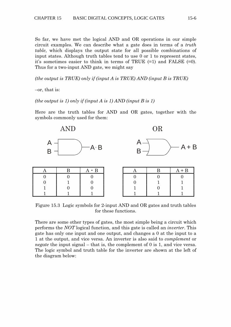
So far, we have met the logical AND and OR operations in our simple circuit examples. We can describe what a gate does in terms of a truth table, which displays the output state for all possible combinations of input states. Although truth tables tend to use 0 or 1 to represent states, it’s sometimes easier to think in terms of TRUE (=1) and FALSE (=0). Thus for a two-input AND gate, we might say (the output is TRUE) only if (input A is TRUE) AND (input B is TRUE) –or, that is: (the output is 1) only if (input A is 1) AND (input B is 1) Here are the truth tables for AND and OR gates, together with the symbols commonly used for them:
AB
AND
A B
AB
OR
A + B
A B A • B A B A + B 0 0 0 0 0 0 0 1 0 0 1 1 1 0 0 1 0 1 1 1 1 1 1 1
Figure 15.3 Logic symbols for 2-input AND and OR gates and truth tables
for these functions. There are some other types of gates, the most simple being a circuit which performs the NOT logical function, and this gate is called an inverter. This gate has only one input and one output, and changes a 0 at the input to a 1 at the output, and vice versa. An inverter is also said to complement or negate the input signal – that is, the complement of 0 is 1, and vice versa. The logic symbol and truth table for the inverter are shown at the left of the diagram below:
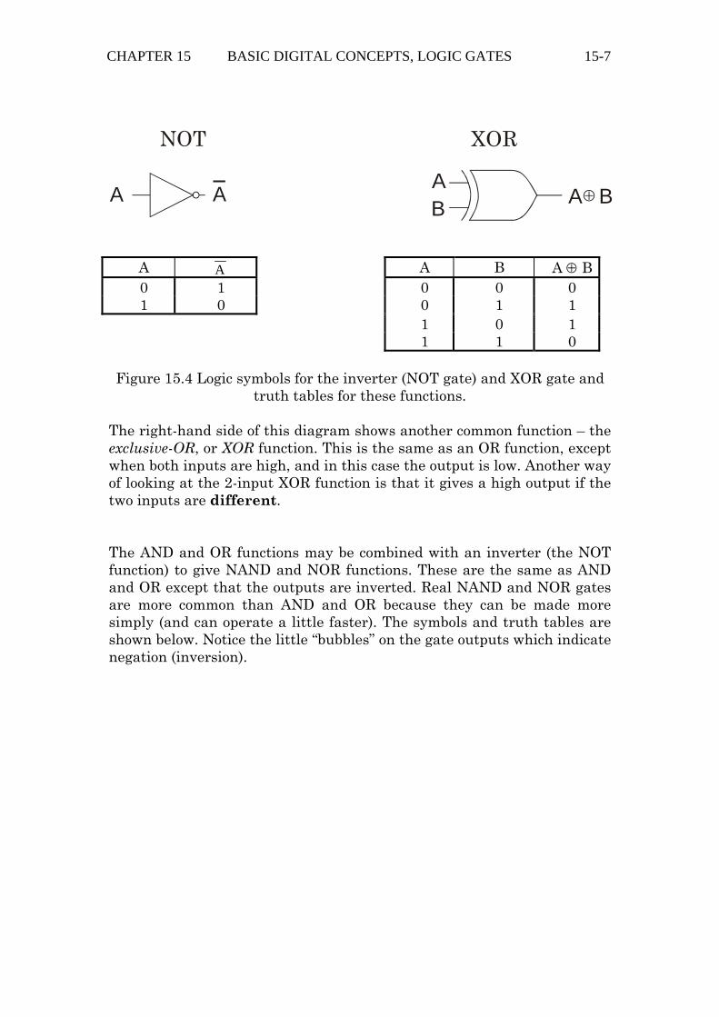
CHAPTER 15 BASIC DIGITAL CONCEPTS, LOGIC GATES 15-7
A
NOT
A
AB
XOR
A B⊕
A A A B A ⊕ B 0 1 0 0 0 1 0 0 1 1 1 0 1 1 1 0
Figure 15.4 Logic symbols for the inverter (NOT gate) and XOR gate and
truth tables for these functions. The right-hand side of this diagram shows another common function – the exclusive-OR, or XOR function. This is the same as an OR function, except when both inputs are high, and in this case the output is low. Another way of looking at the 2-input XOR function is that it gives a high output if the two inputs are different. The AND and OR functions may be combined with an inverter (the NOT function) to give NAND and NOR functions. These are the same as AND and OR except that the outputs are inverted. Real NAND and NOR gates are more common than AND and OR because they can be made more simply (and can operate a little faster). The symbols and truth tables are shown below. Notice the little “bubbles” on the gate outputs which indicate negation (inversion).
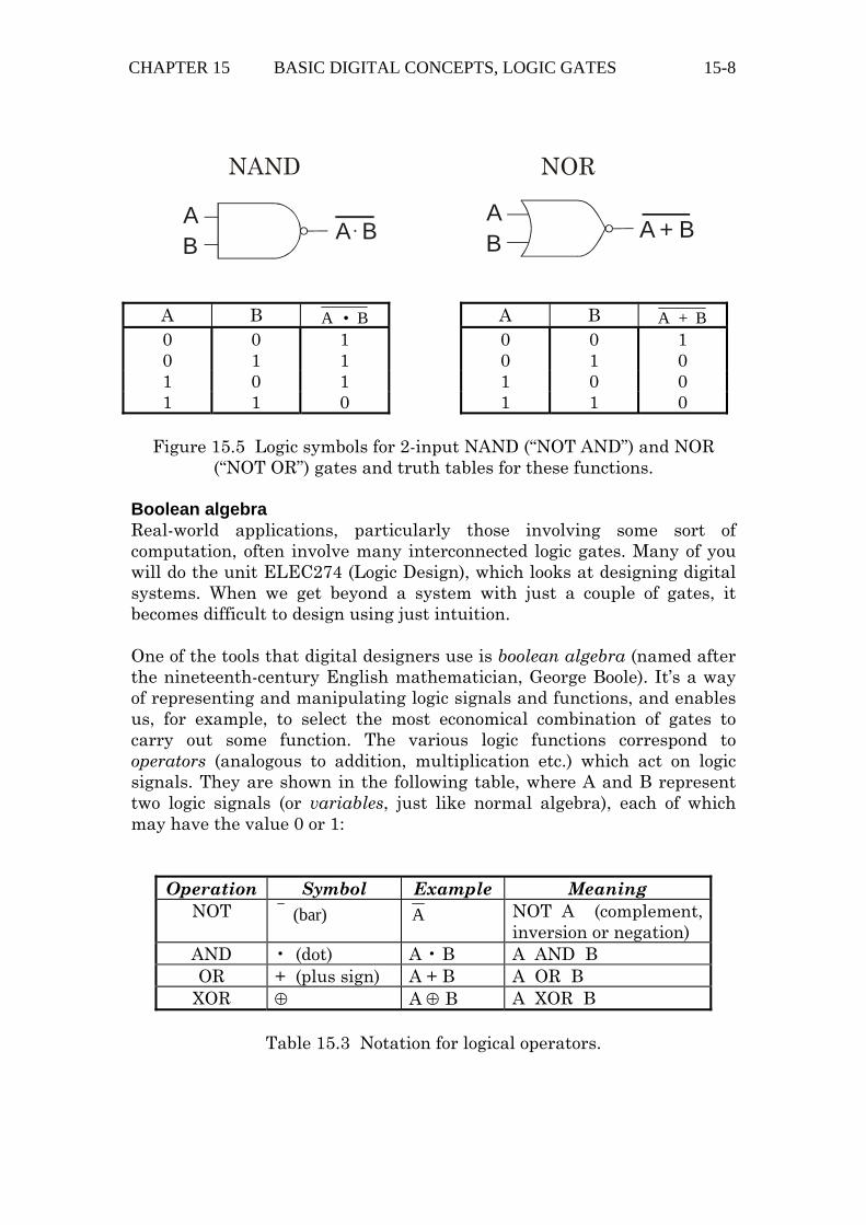
CHAPTER 15 BASIC DIGITAL CONCEPTS, LOGIC GATES 15-8
AB
NAND
A B
AB
NOR
A + B
A B A • B A B A + B 0 0 1 0 0 1 0 1 1 0 1 0 1 0 1 1 0 0 1 1 0 1 1 0
Figure 15.5 Logic symbols for 2-input NAND (“NOT AND”) and NOR
(“NOT OR”) gates and truth tables for these functions. Boolean algebra Real-world applications, particularly those involving some sort of computation, often involve many interconnected logic gates. Many of you will do the unit ELEC274 (Logic Design), which looks at designing digital systems. When we get beyond a system with just a couple of gates, it becomes difficult to design using just intuition. One of the tools that digital designers use is boolean algebra (named after the nineteenth-century English mathematician, George Boole). It’s a way of representing and manipulating logic signals and functions, and enables us, for example, to select the most economical combination of gates to carry out some function. The various logic functions correspond to operators (analogous to addition, multiplication etc.) which act on logic signals. They are shown in the following table, where A and B represent two logic signals (or variables, just like normal algebra), each of which may have the value 0 or 1:
Operation Symbol Example Meaning NOT (bar) A NOT A (complement,
inversion or negation) AND • (dot) A • B A AND B OR + (plus sign) A + B A OR B
XOR ⊕ A ⊕ B A XOR B
Table 15.3 Notation for logical operators.
CHAPTER 15 BASIC DIGITAL CONCEPTS, LOGIC GATES 15-9
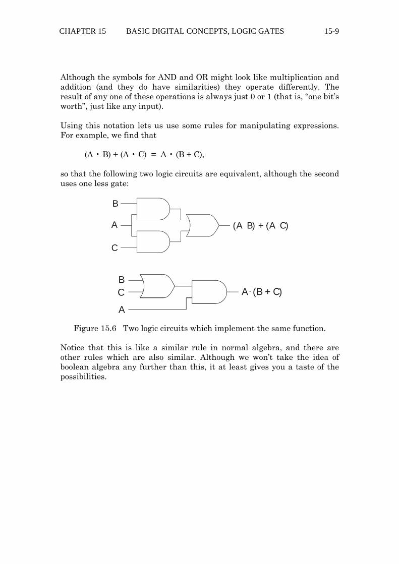
Although the symbols for AND and OR might look like multiplication and addition (and they do have similarities) they operate differently. The result of any one of these operations is always just 0 or 1 (that is, “one bit’s worth”, just like any input). Using this notation lets us use some rules for manipulating expressions. For example, we find that (A • B) + (A • C) = A • (B + C), so that the following two logic circuits are equivalent, although the second uses one less gate:
(A B) + (A C)
B
A
C
A (B + C)BC
A
Figure 15.6 Two logic circuits which implement the same function. Notice that this is like a similar rule in normal algebra, and there are other rules which are also similar. Although we won’t take the idea of boolean algebra any further than this, it at least gives you a taste of the possibilities.
CHAPTER 15 BASIC DIGITAL CONCEPTS, LOGIC GATES 15-10
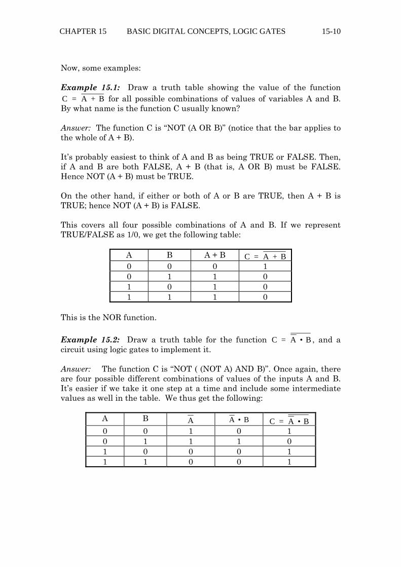
Now, some examples: Example 15.1: Draw a truth table showing the value of the function C = A + B for all possible combinations of values of variables A and B. By what name is the function C usually known? Answer: The function C is “NOT (A OR B)” (notice that the bar applies to the whole of A + B). It’s probably easiest to think of A and B as being TRUE or FALSE. Then, if A and B are both FALSE, A + B (that is, A OR B) must be FALSE. Hence NOT (A + B) must be TRUE. On the other hand, if either or both of A or B are TRUE, then A + B is TRUE; hence NOT (A + B) is FALSE. This covers all four possible combinations of A and B. If we represent TRUE/FALSE as 1/0, we get the following table:
A B A + B C = A + B 0 0 0 1 0 1 1 0 1 0 1 0 1 1 1 0
This is the NOR function.
Example 15.2: Draw a truth table for the function C = A • B , and a circuit using logic gates to implement it. Answer: The function C is “NOT ( (NOT A) AND B)”. Once again, there are four possible different combinations of values of the inputs A and B. It’s easier if we take it one step at a time and include some intermediate values as well in the table. We thus get the following:
A B A A • B C = A • B 0 0 1 0 1 0 1 1 1 0 1 0 0 0 1 1 1 0 0 1
CHAPTER 15 BASIC DIGITAL CONCEPTS, LOGIC GATES 15-11
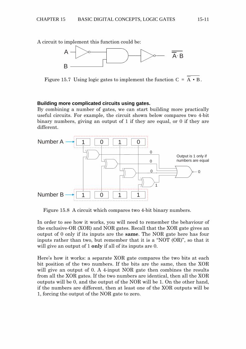
A circuit to implement this function could be:
A B
B
A
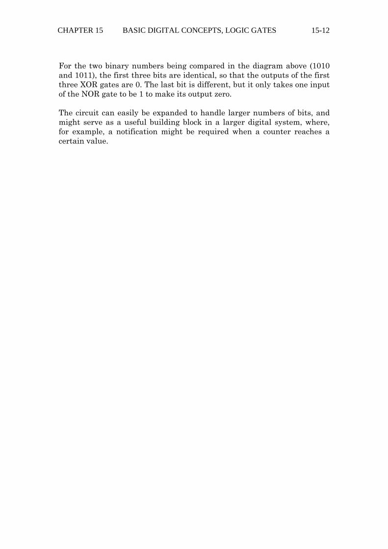
Figure 15.7 Using logic gates to implement the function C = A • B . Building more complicated circuits using gates. By combining a number of gates, we can start building more practically useful circuits. For example, the circuit shown below compares two 4-bit binary numbers, giving an output of 1 if they are equal, or 0 if they are different.
1
1
1
1
0
0
0
1
0
0
0
1
0
Number A
Number B
Output is 1 only ifnumbers are equal
Figure 15.8 A circuit which compares two 4-bit binary numbers. In order to see how it works, you will need to remember the behaviour of the exclusive-OR (XOR) and NOR gates. Recall that the XOR gate gives an output of 0 only if its inputs are the same. The NOR gate here has four inputs rather than two, but remember that it is a “NOT (OR)”, so that it will give an output of 1 only if all of its inputs are 0. Here’s how it works: a separate XOR gate compares the two bits at each bit position of the two numbers. If the bits are the same, then the XOR will give an output of 0. A 4-input NOR gate then combines the results from all the XOR gates. If the two numbers are identical, then all the XOR outputs will be 0, and the output of the NOR will be 1. On the other hand, if the numbers are different, then at least one of the XOR outputs will be 1, forcing the output of the NOR gate to zero.
CHAPTER 15 BASIC DIGITAL CONCEPTS, LOGIC GATES 15-12
For the two binary numbers being compared in the diagram above (1010 and 1011), the first three bits are identical, so that the outputs of the first three XOR gates are 0. The last bit is different, but it only takes one input of the NOR gate to be 1 to make its output zero. The circuit can easily be expanded to handle larger numbers of bits, and might serve as a useful building block in a larger digital system, where, for example, a notification might be required when a counter reaches a certain value.
CHAPTER 16 FLIP-FLOPS, REGISTERS AND COUNTERS 16-1
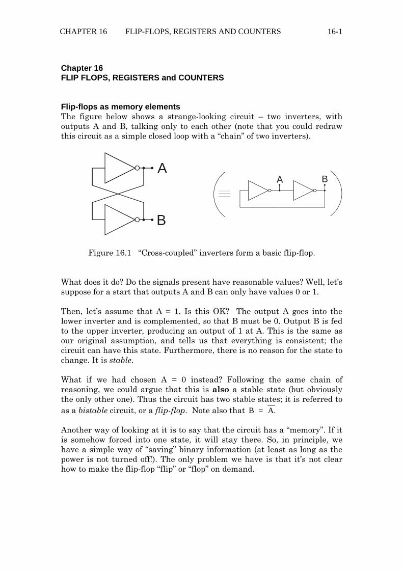
Chapter 16 FLIP FLOPS, REGISTERS and COUNTERS Flip-flops as memory elements The figure below shows a strange-looking circuit – two inverters, with outputs A and B, talking only to each other (note that you could redraw this circuit as a simple closed loop with a “chain” of two inverters).
A
B
A B
Figure 16.1 “Cross-coupled” inverters form a basic flip-flop.
What does it do? Do the signals present have reasonable values? Well, let’s suppose for a start that outputs A and B can only have values 0 or 1. Then, let’s assume that A = 1. Is this OK? The output A goes into the lower inverter and is complemented, so that B must be 0. Output B is fed to the upper inverter, producing an output of 1 at A. This is the same as our original assumption, and tells us that everything is consistent; the circuit can have this state. Furthermore, there is no reason for the state to change. It is stable. What if we had chosen A = 0 instead? Following the same chain of reasoning, we could argue that this is also a stable state (but obviously the only other one). Thus the circuit has two stable states; it is referred to as a bistable circuit, or a flip-flop. Note also that B = A. Another way of looking at it is to say that the circuit has a “memory”. If it is somehow forced into one state, it will stay there. So, in principle, we have a simple way of “saving” binary information (at least as long as the power is not turned off!). The only problem we have is that it’s not clear how to make the flip-flop “flip” or “flop” on demand.
CHAPTER 16 FLIP-FLOPS, REGISTERS AND COUNTERS 16-2
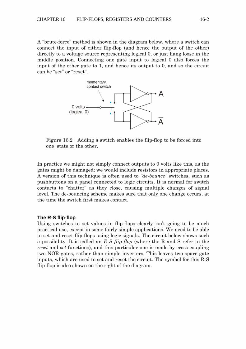
A “brute-force” method is shown in the diagram below, where a switch can connect the input of either flip-flop (and hence the output of the other) directly to a voltage source representing logical 0, or just hang loose in the middle position. Connecting one gate input to logical 0 also forces the input of the other gate to 1, and hence its output to 0, and so the circuit can be “set” or “reset”.
A
A(logical 0)
0 volts
momentary contact switch
Figure 16.2 Adding a switch enables the flip-flop to be forced into one state or the other.
In practice we might not simply connect outputs to 0 volts like this, as the gates might be damaged; we would include resistors in appropriate places. A version of this technique is often used to “de-bounce” switches, such as pushbuttons on a panel connected to logic circuits. It is normal for switch contacts to “chatter” as they close, causing multiple changes of signal level. The de-bouncing scheme makes sure that only one change occurs, at the time the switch first makes contact. The R-S flip-flop Using switches to set values in flip-flops clearly isn’t going to be much practical use, except in some fairly simple applications. We need to be able to set and reset flip-flops using logic signals. The circuit below shows such a possibility. It is called an R-S flip-flop (where the R and S refer to the reset and set functions), and this particular one is made by cross-coupling two NOR gates, rather than simple inverters. This leaves two spare gate inputs, which are used to set and reset the circuit. The symbol for this R-S flip-flop is also shown on the right of the diagram.
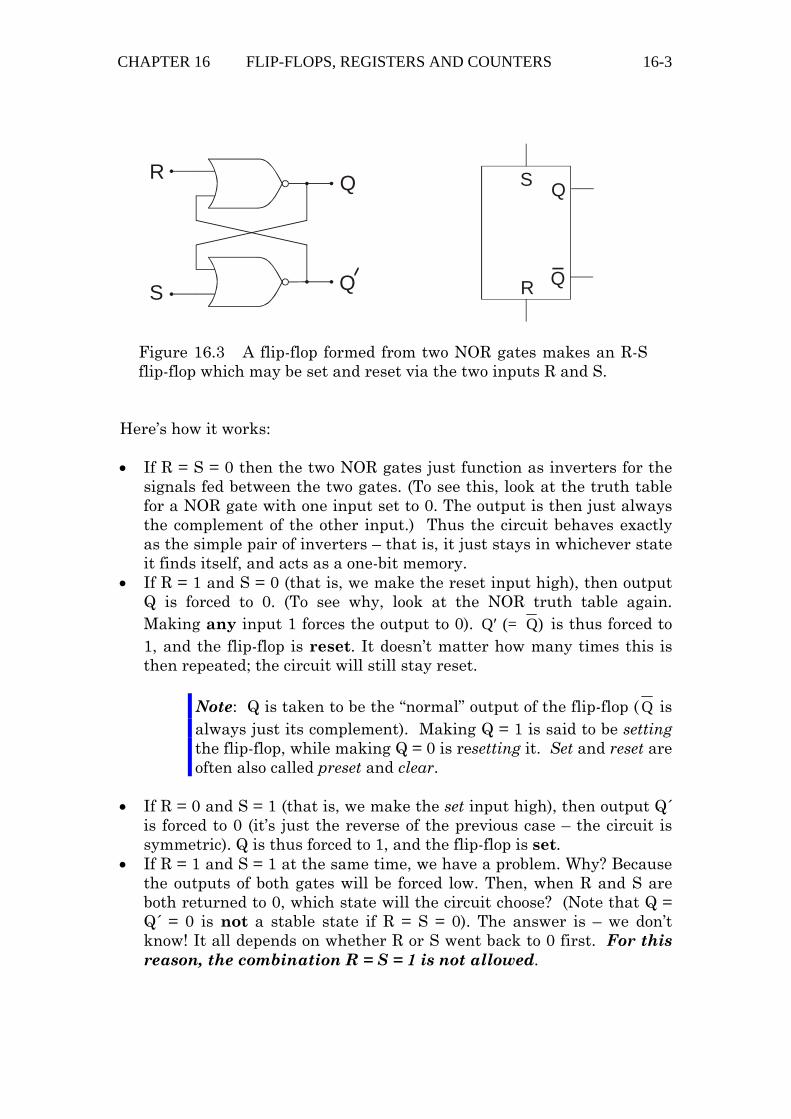
CHAPTER 16 FLIP-FLOPS, REGISTERS AND COUNTERS 16-3
R
S
Q
Q
R
S Q
Q
Figure 16.3 A flip-flop formed from two NOR gates makes an R-S flip-flop which may be set and reset via the two inputs R and S.
Here’s how it works: • If R = S = 0 then the two NOR gates just function as inverters for the
signals fed between the two gates. (To see this, look at the truth table for a NOR gate with one input set to 0. The output is then just always the complement of the other input.) Thus the circuit behaves exactly as the simple pair of inverters – that is, it just stays in whichever state it finds itself, and acts as a one-bit memory.
• If R = 1 and S = 0 (that is, we make the reset input high), then output Q is forced to 0. (To see why, look at the NOR truth table again. Making any input 1 forces the output to 0). ′Q (= Q) is thus forced to 1, and the flip-flop is reset. It doesn’t matter how many times this is then repeated; the circuit will still stay reset.
Note: Q is taken to be the “normal” output of the flip-flop ( Q is always just its complement). Making Q = 1 is said to be setting the flip-flop, while making Q = 0 is resetting it. Set and reset are often also called preset and clear.
• If R = 0 and S = 1 (that is, we make the set input high), then output Q´
is forced to 0 (it’s just the reverse of the previous case – the circuit is symmetric). Q is thus forced to 1, and the flip-flop is set.
• If R = 1 and S = 1 at the same time, we have a problem. Why? Because the outputs of both gates will be forced low. Then, when R and S are both returned to 0, which state will the circuit choose? (Note that Q = Q´ = 0 is not a stable state if R = S = 0). The answer is – we don’t know! It all depends on whether R or S went back to 0 first. For this reason, the combination R = S = 1 is not allowed.
CHAPTER 16 FLIP-FLOPS, REGISTERS AND COUNTERS 16-4
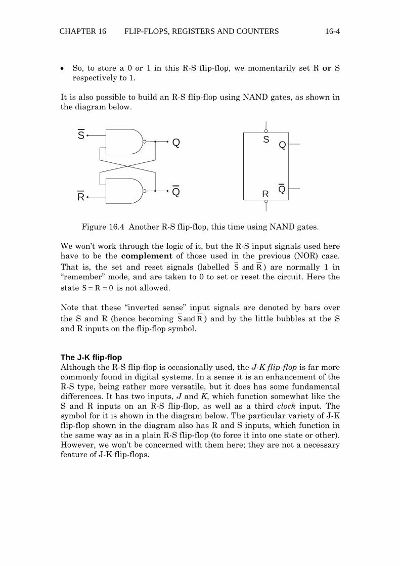
• So, to store a 0 or 1 in this R-S flip-flop, we momentarily set R or S respectively to 1.
It is also possible to build an R-S flip-flop using NAND gates, as shown in the diagram below.
R
SQ
Q
R
S Q
Q
Figure 16.4 Another R-S flip-flop, this time using NAND gates. We won’t work through the logic of it, but the R-S input signals used here have to be the complement of those used in the previous (NOR) case. That is, the set and reset signals (labelled S and R ) are normally 1 in “remember” mode, and are taken to 0 to set or reset the circuit. Here the state 0RS == is not allowed. Note that these “inverted sense” input signals are denoted by bars over the S and R (hence becoming R and S ) and by the little bubbles at the S and R inputs on the flip-flop symbol. The J-K flip-flop Although the R-S flip-flop is occasionally used, the J-K flip-flop is far more commonly found in digital systems. In a sense it is an enhancement of the R-S type, being rather more versatile, but it does has some fundamental differences. It has two inputs, J and K, which function somewhat like the S and R inputs on an R-S flip-flop, as well as a third clock input. The symbol for it is shown in the diagram below. The particular variety of J-K flip-flop shown in the diagram also has R and S inputs, which function in the same way as in a plain R-S flip-flop (to force it into one state or other). However, we won’t be concerned with them here; they are not a necessary feature of J-K flip-flops.
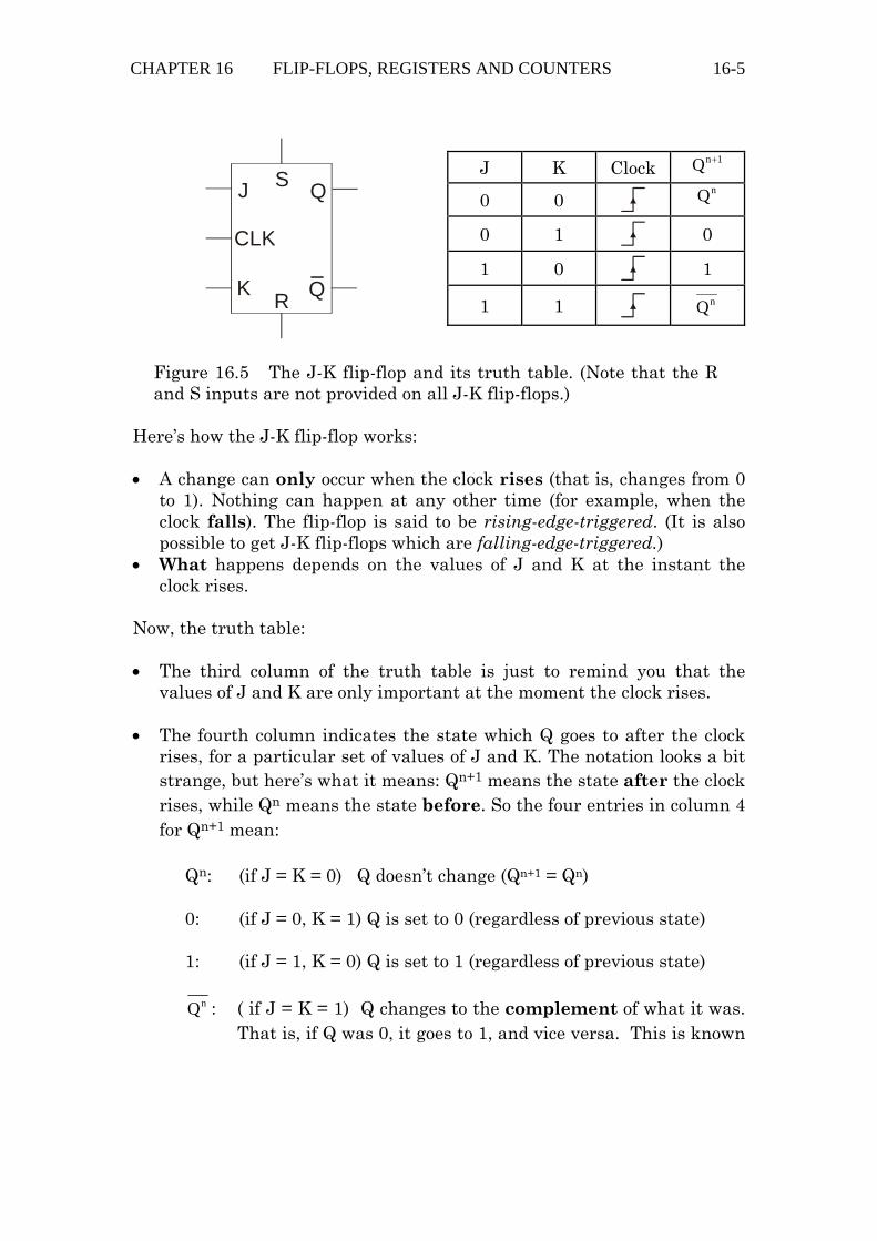
CHAPTER 16 FLIP-FLOPS, REGISTERS AND COUNTERS 16-5
R
S Q
Q
J
CLK
K
J K Clock 1nQ +
0 0 nQ
0 1 0
1 0 1
1 1 ____
nQ
Figure 16.5 The J-K flip-flop and its truth table. (Note that the R and S inputs are not provided on all J-K flip-flops.)
Here’s how the J-K flip-flop works: • A change can only occur when the clock rises (that is, changes from 0
to 1). Nothing can happen at any other time (for example, when the clock falls). The flip-flop is said to be rising-edge-triggered. (It is also possible to get J-K flip-flops which are falling-edge-triggered.)
• What happens depends on the values of J and K at the instant the clock rises.
Now, the truth table: • The third column of the truth table is just to remind you that the
values of J and K are only important at the moment the clock rises. • The fourth column indicates the state which Q goes to after the clock
rises, for a particular set of values of J and K. The notation looks a bit strange, but here’s what it means: Qn+1 means the state after the clock rises, while Qn means the state before. So the four entries in column 4 for Qn+1 mean:
Qn: (if J = K = 0) Q doesn’t change (Qn+1 = Qn) 0: (if J = 0, K = 1) Q is set to 0 (regardless of previous state) 1: (if J = 1, K = 0) Q is set to 1 (regardless of previous state)
:Qn ( if J = K = 1) Q changes to the complement of what it was. That is, if Q was 0, it goes to 1, and vice versa. This is known
CHAPTER 16 FLIP-FLOPS, REGISTERS AND COUNTERS 16-6
as toggling. Note that this behaviour did not occur with the R-S flip-flop.
The J-K truth table is actually not too difficult to remember. The rules are: (1) Things only happen when the clock rises. (2) If J = K = 0 then nothing happens. (3) If J = K = 1 then the flip-flop toggles (4) If J ≠ K then Q goes to the value that J has. The J-K flip-flop has some advantages over the R-S type. First, because changes are controlled by the clock, the operation of many circuits can be synchronised. Second, the behaviour is defined for all values of J and K (remember that R = S = 1 was not allowed with the R-S flip-flop). Third, the toggling behaviour when J = K = 1 allows us to design circuits which do some neat things. There are many useful circuits we can build by connecting J-K flip-flops together. Two of the most important are shift registers and counters. Let’s look at some of these. Shift registers In digital parlance, a register is simply a fancy name for a memory circuit to hold one “chunk” of information consisting of a number of bits. A shift register has the ability to “shift” all the bits of the binary number contained in it one place to the left (or right, or either, depending on its design), for each “tick” of a clock. It’s exactly like having a full row of seats at the cinema, each seating a girl (1) or boy (0). Some newcomer wants to sit at the end, so everybody shifts along by one at the same time to accommodate them. Of course, somebody also gets dropped off the other end, since there are only a fixed number of seats. So the situation might look like this: Before shift: 1 → 1010101100110100 (new girl) After shift: 1101010110011010 → 0 (boy lost off end) The figure below shows a single stage of a shift register using a J-K flip-flop. J is set to the new value to be shifted in, while K is set to its complement (this is easy to arrange with an inverter if necessary). When the clock rises, the J and K values are transferred to Q and Q respectively
CHAPTER 16 FLIP-FLOPS, REGISTERS AND COUNTERS 16-7
(refer back to the J-K truth table to see why). The old values of Q and Q are lost from this flip-flop, but are shifted to the following stage at the same time.
Q
Q
J
CLK
K
A
A
Figure 16.6 A basic shift register stage. With complementary J and K inputs, the data at J and K are transferred to Q and Q on rising clock edges.
We can string together as many basic stages as we like, each feeding the next, as shown in the 3-stage example below. Note that the same clock signal connects to all stages. After the clock rises each time, a new value must be present at the input (A) to get shifted into the register.
Q1 Q2 Q3
Q1 Q2 Q3
J1 J2 J3
CLK CLK CLK
K1 K2 K3
A
A
Clock
to nextstages
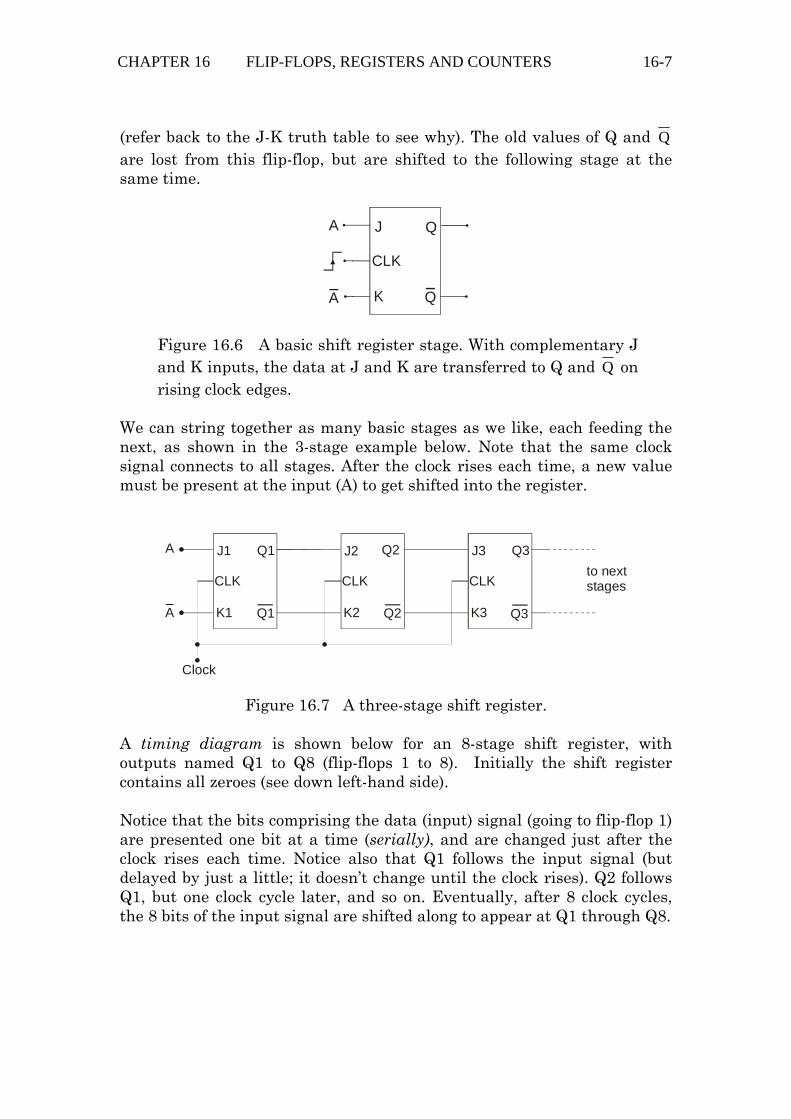
Figure 16.7 A three-stage shift register. A timing diagram is shown below for an 8-stage shift register, with outputs named Q1 to Q8 (flip-flops 1 to 8). Initially the shift register contains all zeroes (see down left-hand side). Notice that the bits comprising the data (input) signal (going to flip-flop 1) are presented one bit at a time (serially), and are changed just after the clock rises each time. Notice also that Q1 follows the input signal (but delayed by just a little; it doesn’t change until the clock rises). Q2 follows Q1, but one clock cycle later, and so on. Eventually, after 8 clock cycles, the 8 bits of the input signal are shifted along to appear at Q1 through Q8.
CHAPTER 16 FLIP-FLOPS, REGISTERS AND COUNTERS 16-8
Clock
Q1
Q2
Q3
Q4
Q5
Q6
Q7
Q8
Data 1 0 1 1 0 0 0 1
1
0
0
0
1
1
0
1
Figure 16.8 Timing diagram for serial-to-parallel conversion using an 8-bit shift register. Q1 to Q8 are all initially 0, but after 8 clock cycles are set to the values of the incoming serial data.
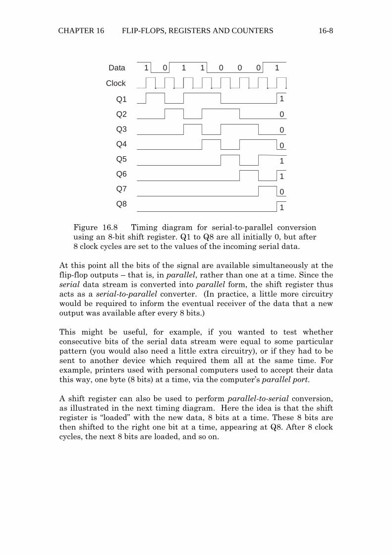
At this point all the bits of the signal are available simultaneously at the flip-flop outputs – that is, in parallel, rather than one at a time. Since the serial data stream is converted into parallel form, the shift register thus acts as a serial-to-parallel converter. (In practice, a little more circuitry would be required to inform the eventual receiver of the data that a new output was available after every 8 bits.) This might be useful, for example, if you wanted to test whether consecutive bits of the serial data stream were equal to some particular pattern (you would also need a little extra circuitry), or if they had to be sent to another device which required them all at the same time. For example, printers used with personal computers used to accept their data this way, one byte (8 bits) at a time, via the computer’s parallel port. A shift register can also be used to perform parallel-to-serial conversion, as illustrated in the next timing diagram. Here the idea is that the shift register is “loaded” with the new data, 8 bits at a time. These 8 bits are then shifted to the right one bit at a time, appearing at Q8. After 8 clock cycles, the next 8 bits are loaded, and so on.
CHAPTER 16 FLIP-FLOPS, REGISTERS AND COUNTERS 16-9
Clock
Q1
Q2
Q3
Q4
Q5
Q6
Q7
Q8 1 0 1 1 0 0 0 1
1
0
0
0
1
1
0
Figure 16.9 Timing diagram for parallel-to-serial conversion using an 8-bit shift register.
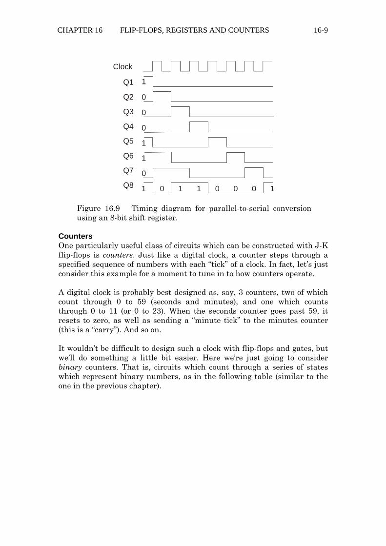
Counters One particularly useful class of circuits which can be constructed with J-K flip-flops is counters. Just like a digital clock, a counter steps through a specified sequence of numbers with each “tick” of a clock. In fact, let’s just consider this example for a moment to tune in to how counters operate. A digital clock is probably best designed as, say, 3 counters, two of which count through 0 to 59 (seconds and minutes), and one which counts through 0 to 11 (or 0 to 23). When the seconds counter goes past 59, it resets to zero, as well as sending a “minute tick” to the minutes counter (this is a “carry”). And so on. It wouldn’t be difficult to design such a clock with flip-flops and gates, but we’ll do something a little bit easier. Here we’re just going to consider binary counters. That is, circuits which count through a series of states which represent binary numbers, as in the following table (similar to the one in the previous chapter).
CHAPTER 16 FLIP-FLOPS, REGISTERS AND COUNTERS 16-10
Decimal Binary Decimal Binary
0 0000 8 1000 1 0001 9 1001 2 0010 10 1010 3 0011 11 1011 4 0100 12 1100 5 0101 13 1101 6 0110 14 1110 7 0111 15 1111
Table 16.1 Successive states of a 4-bit binary counter counting from 0 to 15 (decimal).
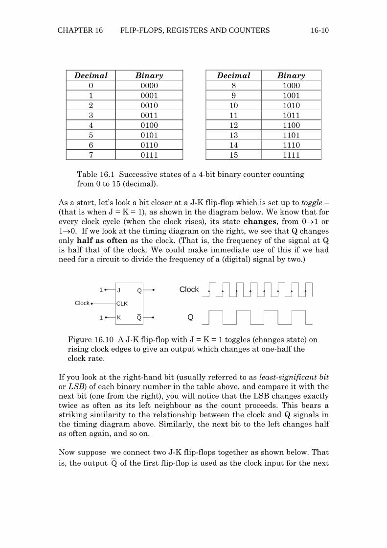
As a start, let’s look a bit closer at a J-K flip-flop which is set up to toggle – (that is when J = K = 1), as shown in the diagram below. We know that for every clock cycle (when the clock rises), its state changes, from 0→1 or 1→0. If we look at the timing diagram on the right, we see that Q changes only half as often as the clock. (That is, the frequency of the signal at Q is half that of the clock. We could make immediate use of this if we had need for a circuit to divide the frequency of a (digital) signal by two.)
Q
Q
J
CLK
K
1
Clock
1
Clock
Q
Figure 16.10 A J-K flip-flop with J = K = 1 toggles (changes state) on rising clock edges to give an output which changes at one-half the clock rate.
If you look at the right-hand bit (usually referred to as least-significant bit or LSB) of each binary number in the table above, and compare it with the next bit (one from the right), you will notice that the LSB changes exactly twice as often as its left neighbour as the count proceeds. This bears a striking similarity to the relationship between the clock and Q signals in the timing diagram above. Similarly, the next bit to the left changes half as often again, and so on. Now suppose we connect two J-K flip-flops together as shown below. That is, the output Q of the first flip-flop is used as the clock input for the next
CHAPTER 16 FLIP-FLOPS, REGISTERS AND COUNTERS 16-11
flip-flop. The output of the second flip-flop will now change at one-quarter the rate of the clock.
Q1 Q2
Q1 Q2
J1 J2
CLK CLK
K1 K2
1 1
1 1
Clock
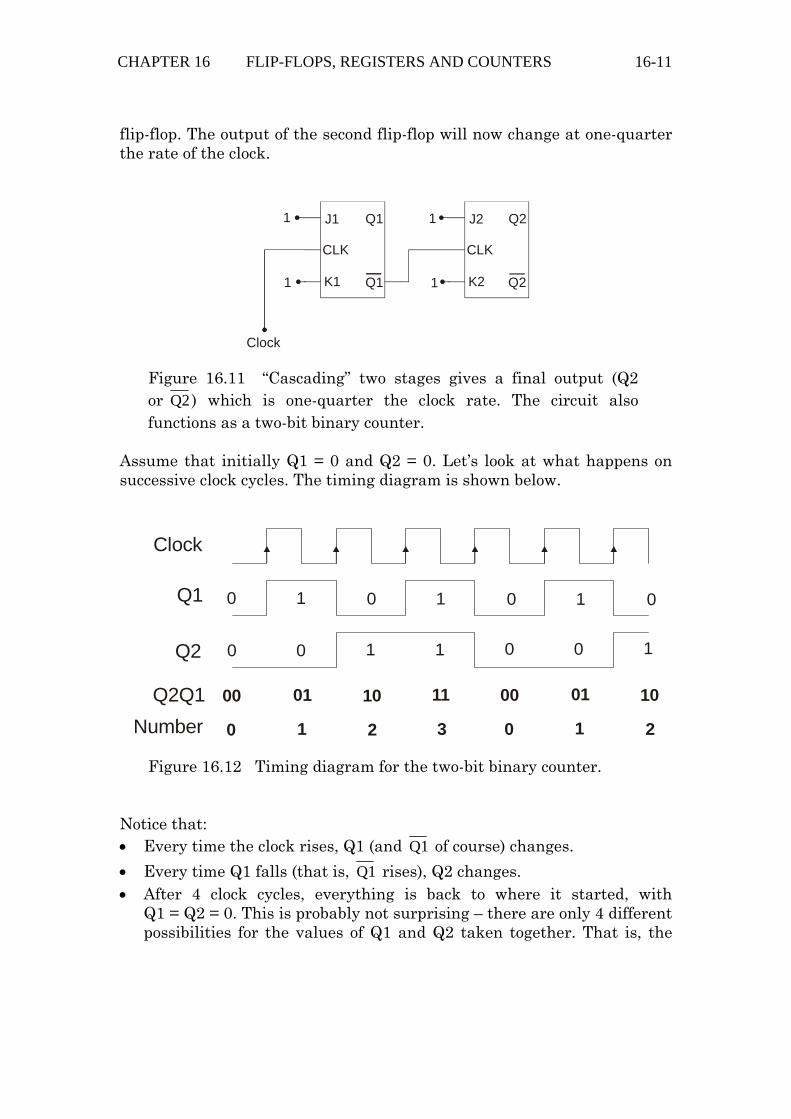
Figure 16.11 “Cascading” two stages gives a final output (Q2 or Q2 ) which is one-quarter the clock rate. The circuit also functions as a two-bit binary counter.
Assume that initially Q1 = 0 and Q2 = 0. Let’s look at what happens on successive clock cycles. The timing diagram is shown below.
Clock
Q1
Q2
Q2Q1Number
0
0 1 0 1
0 0 01
0 1 0
1 1
00 0001 0110 1011
0 01 12 23
Figure 16.12 Timing diagram for the two-bit binary counter.
Notice that: • Every time the clock rises, Q1 (and Q1 of course) changes.
• Every time Q1 falls (that is, Q1 rises), Q2 changes. • After 4 clock cycles, everything is back to where it started, with
Q1 = Q2 = 0. This is probably not surprising – there are only 4 different possibilities for the values of Q1 and Q2 taken together. That is, the
CHAPTER 16 FLIP-FLOPS, REGISTERS AND COUNTERS 16-12
whole circuit has only 4 different possible states. It certainly can’t take longer than 4 clock cycles to return!
• Taken together as a binary number, the pair {Q2Q1} cycles through the values 00, 01, 10, 11, …(decimal 0, 1, 2, 3,…). That is, we have constructed a 2-bit binary counter.
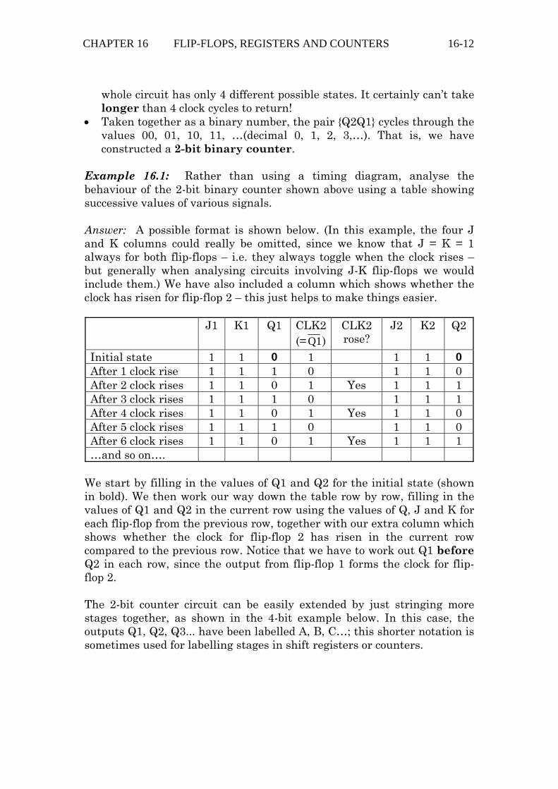
Example 16.1: Rather than using a timing diagram, analyse the behaviour of the 2-bit binary counter shown above using a table showing successive values of various signals. Answer: A possible format is shown below. (In this example, the four J and K columns could really be omitted, since we know that J = K = 1 always for both flip-flops – i.e. they always toggle when the clock rises – but generally when analysing circuits involving J-K flip-flops we would include them.) We have also included a column which shows whether the clock has risen for flip-flop 2 – this just helps to make things easier.
J1 K1 Q1 CLK2 (= Q1)
CLK2 rose?
J2 K2 Q2
Initial state 1 1 0 1 1 1 0 After 1 clock rise 1 1 1 0 1 1 0 After 2 clock rises 1 1 0 1 Yes 1 1 1 After 3 clock rises 1 1 1 0 1 1 1 After 4 clock rises 1 1 0 1 Yes 1 1 0 After 5 clock rises 1 1 1 0 1 1 0 After 6 clock rises 1 1 0 1 Yes 1 1 1 …and so on….
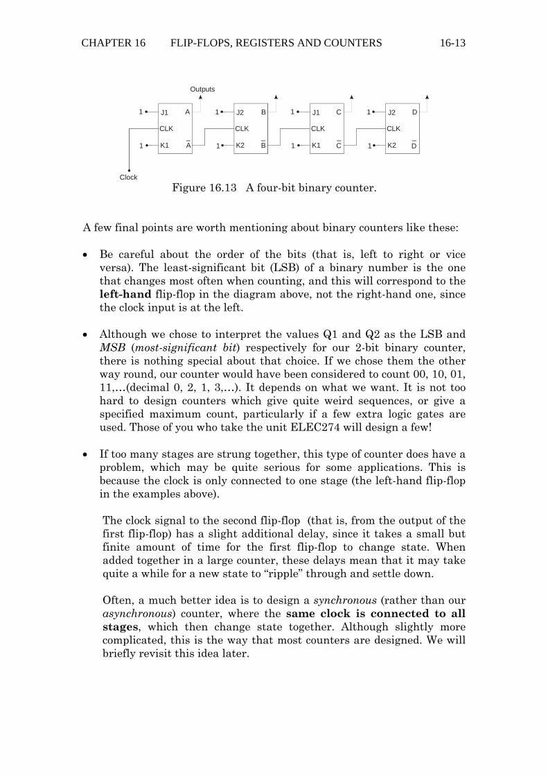
We start by filling in the values of Q1 and Q2 for the initial state (shown in bold). We then work our way down the table row by row, filling in the values of Q1 and Q2 in the current row using the values of Q, J and K for each flip-flop from the previous row, together with our extra column which shows whether the clock for flip-flop 2 has risen in the current row compared to the previous row. Notice that we have to work out Q1 before Q2 in each row, since the output from flip-flop 1 forms the clock for flip-flop 2. The 2-bit counter circuit can be easily extended by just stringing more stages together, as shown in the 4-bit example below. In this case, the outputs Q1, Q2, Q3... have been labelled A, B, C…; this shorter notation is sometimes used for labelling stages in shift registers or counters.
CHAPTER 16 FLIP-FLOPS, REGISTERS AND COUNTERS 16-13
A CB D
A CB D
J1 J1J2 J2
CLK CLKCLK CLK
K1 K1K2 K2
1 11 1
1 11 1
Clock
Outputs
Figure 16.13 A four-bit binary counter.
A few final points are worth mentioning about binary counters like these: • Be careful about the order of the bits (that is, left to right or vice
versa). The least-significant bit (LSB) of a binary number is the one that changes most often when counting, and this will correspond to the left-hand flip-flop in the diagram above, not the right-hand one, since the clock input is at the left.
• Although we chose to interpret the values Q1 and Q2 as the LSB and
MSB (most-significant bit) respectively for our 2-bit binary counter, there is nothing special about that choice. If we chose them the other way round, our counter would have been considered to count 00, 10, 01, 11,…(decimal 0, 2, 1, 3,…). It depends on what we want. It is not too hard to design counters which give quite weird sequences, or give a specified maximum count, particularly if a few extra logic gates are used. Those of you who take the unit ELEC274 will design a few!
• If too many stages are strung together, this type of counter does have a
problem, which may be quite serious for some applications. This is because the clock is only connected to one stage (the left-hand flip-flop in the examples above).
The clock signal to the second flip-flop (that is, from the output of the first flip-flop) has a slight additional delay, since it takes a small but finite amount of time for the first flip-flop to change state. When added together in a large counter, these delays mean that it may take quite a while for a new state to “ripple” through and settle down. Often, a much better idea is to design a synchronous (rather than our asynchronous) counter, where the same clock is connected to all stages, which then change state together. Although slightly more complicated, this is the way that most counters are designed. We will briefly revisit this idea later.
CHAPTER 16 FLIP-FLOPS, REGISTERS AND COUNTERS 16-14
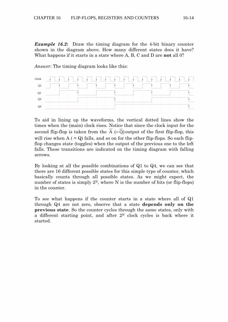
Example 16.2: Draw the timing diagram for the 4-bit binary counter shown in the diagram above. How many different states does it have? What happens if it starts in a state where A, B, C and D are not all 0? Answer: The timing diagram looks like this: Clock
Q1
Q3
Q2
Q4
To aid in lining up the waveforms, the vertical dotted lines show the times when the (main) clock rises. Notice that since the clock input for the second flip-flop is taken from the )Q ( A = output of the first flip-flop, this will rise when A ( = Q) falls, and so on for the other flip-flops. So each flip-flop changes state (toggles) when the output of the previous one to the left falls. These transitions are indicated on the timing diagram with falling arrows. By looking at all the possible combinations of Q1 to Q4, we can see that there are 16 different possible states for this simple type of counter, which basically counts through all possible states. As we might expect, the number of states is simply 2N, where N is the number of bits (or flip-flops) in the counter. To see what happens if the counter starts in a state where all of Q1 through Q4 are not zero, observe that a state depends only on the previous state. So the counter cycles through the same states, only with a different starting point, and after 2N clock cycles is back where it started.