Embed Size (px)
Citation preview
42
CHAPTER 3
THE INVERTED-L ANTENNA AND VARIATIONS
3.1 Introduction
As the demand for portable and convenient wireless devices becomes stronger, the
need for device miniaturization increases. [1] The size of a wireless device is often limited
by the dimensions of the battery and the antenna. [1] Generally, the quarter-wave
monopole antenna is used on portable wireless devices due to its characteristically high
radiation efficiency and wide bandwidth. [2] However, the monopole antenna is potentially
obtrusive. It is desirable that the antenna in a wireless device be as small and
inconspicuous as possible while still meeting performance demands. Therefore, a need
exists for electrically small, low-profile antenna designs with broad impedance bandwidth,
an input impedance that is easily matched to a feed line, omnidirectional radiation, and
high radiation efficiency. [3]
One low-profile antenna design that is used in wireless applications is the Inverted-
L antenna (ILA). The ILA is a short monopole with the addition of a horizontal segment
of wire at the top. The ILA and a few of its variations are illustrated in Figure 3.1.

43
Inverted - L Inverted - F Planar DualInverted - F Inverted - FAntenna AntennaAntenna Antenna
#1 #2 #3 #4
Figure 3.1. The Inverted-L Antenna (ILA) and variations
This chapter presents design issues for the ILA (#1 in Figure 3.1) and its
variations. In Sections 3.2 and 3.3, closed form solutions for the radiation patterns and
input impedance of the ILA are derived using an assumed current distribution on the
antenna. Section 3.4 covers design issues for variations of the ILA, including the Inverted-
F Antenna (IFA) (#2 in Figure 3.1), the Planar Inverted-F Antenna (PIFA) (#3 in Figure
3.1), and the Dual Inverted-F Antenna (DIFA) (#4 in Figure 3.1).
3.2 The Far-Field Radiation Pattern of the Inverted-L Antenna
The Inverted-L Antenna (ILA) in Figure 3.2 is an electrically small end-fed
monopole with a section of horizontal wire added at the top as a capacitive load.

44
h
L
oI
z
x
Figure 3.2. The geometry of the Inverted-L Antenna (ILA)
The ground plane image of the antenna, shown in Figure 3.2 with dotted lines, is treated
as part of the antenna structure to simplify calculations. [4] The calculations are further
simplified by rotating the Cartesian coordinate system as shown in Figure 3.3.
y
x
z
J (z)
J (z)
J (z)
1
3
2Arm 1
Arm 2
Arm 3
h
L
Figure 3.3. The ILA and rotated Cartesian coordinate system
In Figure 3.3, the vertical element of the ILA is located on the x-axis, and the top
horizontal segment and its image are z-directed with opposing currents. The resonant
current distribution on each of the arms is assumed to be sinusoidal. The distributions are
[4]

45
[ ]I z I k L z khz1( ) sin ( ' ) cos( )= − az (3.1)
[ ]I z I k L z khz2 ( ) sin ( ' ) cos( )= − (-az) (3.2)
I z I kx kLz3( ) cos( ' ) sin( )= ax (3.3)
Using the current distributions in (3.1) through (3.3), the fields due to each arm are
determined by calculating magnetic vector potentials, A, and integrating with respect to
the radiation vector. [4] Arm 1 is z-directed with positive running current. The far-field
magnetic vector potential on arm 1 is
[ ]Ae
rI z e dz
er
I k L z kh e dzz
jkrjkz
L jkr
zjkz
L= = −
− −
∫ ∫4 410 0π πθ θ( ) ' sin ( ') cos( ) ''cos( ) 'cos( ) (3.4)
where r x y z= + +2 2 2 . Using (3.4), the E-field for an offset z-directed line source is
written as [4]
ΕΕ = ⋅ ⋅j kh Azωµ θ θ φsin sin( sin cos ) aθθ (3.5)
Substituting (3.4) into (3.5) gives
[ ]ΕΕ = ⋅ ⋅ −−
∫je
rkh I kh k L z e dz
jkr
zjkz
Lωµ
πθ θ φ θ
4 0sin sin( sin cos ) cos( ) sin ( ' ) ''cos( ) (3.6)
The integration in (3.6) is solved using
[ ]sin( ) sin( ) cos( )a bx e dxe
b cc a bx b a bxcx
cx
+ =+
+ − +∫ 2 2 (3.7)
using (3.7) in (3.6) leads to [4]

46
( )Ej e
rSIN I kh
ek k
jk kL kz k kL kzjkr
z
jkz L
θ
θωµπ
θθ
θ=−
− + −
−
4 2 2 20
sin ( ) cos( )cos
cos sin( ' cos( ' ))'cos
where SIN = sin(kh ⋅ sin(θ) ⋅ cos(φ)). When evaluated and simplified, this expression yields
the θ-component of the E-field produced by the currents on arm 1 of the ILA. The result
is [4]
[ ]Ek
Ie
rkh
SINe j kL kLz
jkrjkL
θθωµ
π θθ= − − ⋅ −
−
4cos( )
sin( )cos sin( ) cos( )cos (3.8)
Since the element is z-directed, Eφ = 0.
By symmetry, the fields produced by the currents on arm 2 of the ILA are identical
to those produced by arm 1. The fields produced by the currents on arm 3 of the structure
are summarized without derivation as [4]
Ej
kI
er
kL f hx
jkr
θωµπ
θ φ θ φ= − ⋅−
4sin( ) cos cos ( , , ) (3.9)
Ej
kI
er
kL f hx
jkr
φωµπ
φ θ φ= ⋅−
4sin( ) sin ( , , ) (3.10)
where
f hkh COS kh SIN
( , , )sin( ) sin cos cos( )
sin cosθ φ θ φ
θ φ= ⋅ − ⋅ ⋅ ⋅
− ⋅1 2 2
in which COS = cos(kh ⋅ sin(θ) ⋅ cos(φ)) and SIN was defined earlier.
The expressions for fields from the various arms of the ILA can be simplified if it is
assumed that Ix = Iz = Io, L = λ/4, and h << λ. Then the fields from arms 1 and 2 of the
ILA are re-written as
Ek
Ie
rkh jo
jkr
θωµπ
φ π θ π θ θ= −
+ −
−
4 2 2cos( ) cos cos sin( cos ) cos (3.11)
and Eφ = 0. The fields due to the currents on arm 3 of the ILA are

47
Ej
kI
er
kho
jkr
θωµπ
θ φ= −−
4cos cos (3.12)
Ej
kI
er
kho
jkr
φωµπ
φ=−
4sin (3.13)
The fields expressed in (3.11) through (3.13) define the radiation fields of the ILA
in the three principal planes, x-y, y-z, and x-z. In the x-y plane, θ = π/2, and the E-fields
are
E Ie
rkho
jkr
θ φ= −−
60 cos( ) from arms 1 and 2, (3.14)
and
E j Ie
rkho
jkr
φ φ=−
60 sin from arm 3. (3.15)
In the x-z plane, φ = 0, and the E-fields are
Ek
Ie
Rkh jo
jkR
θωµπ
πθ
πθ θ= −
+ −
−
4 2 2cos cos sin( cos ) cos from arms 1 and 2, (3.16)
and
Ej
kI
eR
kho
jkR
θωµπ
θ= −−
4cos from arm 3. (3.17)
In the y-z plane, there is no field produced by arms 1 and 2. The field due to arm 3 is
Ej
kI
eR
kho
jkR
φωµπ
φ=−
4sin (3.18)
Thus, the normalized pattern factors in the x-y plane are, for Eθ,
F( ) cos( )φ φ= from arms 1 and 2 (3.19)
and, for Eφ,
( )F( ) sinφ φ= from arm 3 (3.20)
and in the x-z plane

48
F j( ) cos cos sin( cos ) cosθπ
θπ
θ θ=
+ −
2 2
from arms 1 and 2 (3.21)
and
F( ) cos( )θ θ= from arm 3. (3.22)
and in the y-z plane
F( )θ = 1 (3.23)
The radiation patterns of the ILA are plotted in Figure 3.4 using the normalized
pattern factors given by (3.19) through (3.23).
Figure 3.4. The modeled radiation patterns of the Inverted-L Antenna, using the antenna system in
Figure 3.3. [4]
The coordinate system used in Figure 3.4 was defined in Figure 3.3. Figure 3.4(c) shows
that the radiation pattern of the ILA is omni-directional in azimuth. The patterns are
identical to those of a monopole in the y-z and x-y planes. In the x-z plane, however, two
Eθ components are generated, one by arms 1 and 2 and one by arm 3. The components

49
vary in phase and have different points of maximum radiation. When the two components
combine, the nulls in both patterns are filled to give nearly omnidirectional coverage. [4]
Figure 3.4 illustrates how the various current components on the ILA affect the
far-field radiation. In the next section, the input impedance of the ILA is derived by
assuming a sinusoidal current distribution on the antenna.
3.3 The Input Impedance of the Inverted-L Antenna
Before applying Pocklington’s equation to the Inverted-L Antenna (ILA), it is
worth while to review the derivation for a z-directed current source. The electric field
induced by a distributed current on an antenna structure is written as a combination of a
vector potential A, and a scalar potential Φ, [5]
E A= − − ∇Φj oωµ (3.24)
For a z-directed current, (3.24) can be written in scalar form. The result is [5]
E j Azz o z= − −ωµ ∂Φ
∂(3.25)
The Lorentz gauge condition for a z-directed current is [5]
∂∂
ωεAz
jzo= − Φ (3.26)
using the derivative of (3.26) in (3.25), gives [5]
Ej
Az
Azo
zz= +
1 2
22
ωε∂∂
β (3.27)
where β ω µ ε= o o is the phase constant for a plane wave. [5] The free space Green’s
function is given by
Ψ =−e
R
j Rβ
π4(3.28)

50
where R is defined as the distance between the source point, (x’, y’, z’), and the
observation point, (x, y, z), written as
R x x y y z z= − + − + −( ' ) ( ' ) ( ' )2 2 2 (3.29)
For a z-directed element of current, J dv’ [5]
dEj
z zz
z z Jdvzo
= +
1 2
22
ωε∂
∂β
ΨΨ
( , ' )( , ' ) ' (3.30)
The total contribution to the electric field is the integral of (3.30) over the volume
in which the current exists. If the current is running along a cylindrical wire of very high
conductivity, such as that illustrated in Figure 3.5(a), nearly all of the current will exist on
the surface of the wire. [5]
c
J s
L2
L2
(a)
ObservationPoint
a
R
I
(b)
Figure 3.5. (a) Surface current on a cylindrical wire with cross sectional curve c. (b) Equivalent
filamentary line source for (a). [5]

51
If infinite conductivity is assumed, all of the current exists on the surface of the wire, and
the volume integral reduces to [5]
Ej
z zz
z z J dzdzo
s
L
L
c
= +
−∫∫
1 2
22
2
2
ωε∂
∂β φΨ Ψ( , ' )
( , ' )/
/
(3.31)
where c is the cross sectional curve of the wire in Figure 3.5(a), and Js is the current on
the surface of the wire. If the surface current is observed from a point along the wire axis
in Figure 3.5(b),
R z z a= − +( ' )2 2 (3.32)
where a is the radius of the wire. If the wire is sufficiently thin, so that a << λ,
circumferential current does not exist, and the longitudinal current is nearly uniform
around the circumference of the wire. Using this thin wire approximation, (3.31) reduces
to [5]
Ej
z zz
z z I z dzzo L
L
= +
−∫
1 2
22
2
2
ωε∂
∂βΨ Ψ( , ' )
( , ' ) ( ' )/
/
(3.33)
that is the integration of current over the equivalent filamentary line source illustrated in
Figure 3.5(b). Although the integration is over an infinitely thin filament of current, the
cross sectional area of the wire is included since the wire radius, a, is included in (3.32)
and thus in (3.28) and (3.33). [5]
The expression in (3.33) gives the scattered field. [5] At the surface of the
perfectly conducting wire, the scattered field is equal to the incident or impressed field. [5]
Therefore, Ezs = -Ez
i, and
− = +
−∫E
jz z
zz z I z dzz
i
o L
L1 2
22
2
2
ωε∂
∂βΨ Ψ( , ' )
( , ' ) ( ' )/
/
(3.34)
This is the general form of Pocklington’s integral equation, valid for z-directed currents
with the thin wire approximation. [5]

52
Pocklington’s integral equation is formulated to express the fields radiated by an
electrically small ILA by using the z-directed currents on the vertical segment as well as
the x-directed currents on the horizontal segment. In Figure 3.2, the ILA is modeled with
an infinite perfectly conducting ground plane. The ground plane image of the ILA is
treated as part of the antenna structure. Currents flow on the ILA in both the x and z
directions. Therefore, the vector magnetic potential, A, exists in the x and z directions and
the scalar potential, Φ, includes the x and z dimensions. [6] The vector magnetic potential,
and scalar potentials are related to one another by the Lorentz gauge equation: [6]
∂∂
∂∂
ωεΦAx
Az
jx z+ + = 0 (3.35)
Differentiating with respect to z yields
− = +
∂Φ∂ ωε
∂∂
∂∂
∂∂z j
Az z
Ax
z x1 2
2(3.36)
Substituting this expression into (3.25) gives
Ej
AAz z
Axz z
z x= + +
1 22
2ωεβ
∂∂
∂∂
∂∂
(3.37)
The derivation of Pocklington’s integral equation in two dimensions is the same as that for
the general form of Pocklington’s equation, except that (3.25) is replaced by (3.37). The
result is the electric field in the z direction due to both the x and z-directed currents on the
ILA and its image. A two dimensional form of Pocklington’s integral equation that is valid
for radiation problems involving the ILA is [6]
− = +
−∫E
jI z
z zz
z z dzzi
zz
zh
h1
4
2
22
ω πε∂ ψ
∂β ψ( ' )
( , ' )( , ' ) '

53
+
+
∫1
4jI x
zx x zx
dxxtxt
a
L a
ω πε∂∂
∂ψ∂
( ' )( , ' , )
'
+
+
∫1
4jI x
zx x zx
dxxbxb
a
L a
ω πε∂∂
∂ψ∂
( ' )( , ', )
' (3.38)
where the current distributions on each arm of the ILA, Iz(z’), Ixt(x’), and Ixb(x’) are
unknown and the Green’s functions are
ψβ
z
j R
z ze
R( , ' ) =
−
, ψβ
xt
j R
t
x x ze
R
t
( , ' , ) =−
, ψβ
xb
j R
b
x x ze
R
b
( , ', ) =−
where
R z z a= − +( ' )2 2
R h z x xt = − + −( ) ( ' )2 2
R h z x xb = + + −( ) ( ' )2 2
If the ILA is electrically small (kh < 0.5 and kL < 0.5 for k = 2π / λ) , the currents
vary linearly with a maximum at the generator and zero at the free end. [6] Thus, the
unknown current distributions in (3.38) are replaced by
I z Iz
h Lz o( ' )'
= −+
1 for -h ≤ z’ ≤ h (3.39)
I x Ix a h
h Lxt o( ' ) = −− +
+
1 for a ≤ x’ ≤ L + a and z’ = h (3.40)
I x Ix a h
h Lxb o( ' ) = − −− +
+
1 for a ≤ x’ ≤ L + a and z’ = -h (3.41)
An accurate analysis of the current in the bend between the vertical and horizontal
segments is not performed. However, the current entering the bend must equal the current
leaving the bend. Therefore, the current at z’ = h is equivalent to that at x’ = a. [6]
Once the current distribution on the ILA is assumed, the radiated electric fields

54
follow immediately from (3.38). Substituting (3.39) through (3.41) into (3.38) gives the
impressed, or incident z-directed electric field, -Ezi, in terms of an unknown current at the
generator, Io = Iz(0).
Given the impressed electric field, the input impedance of the ILA is derived using
the equivalent circuit in Figure 3.6.
+
-VT
ZA
ZL
-Io
Figure 3.6. Equivalent circuit of the ILA [6]
In Figure 3.6, ZA is the input impedance of the antenna, and the current source at
the feed point of the ILA is replaced by a complex impedance, ZL. The Thevenin voltage,
VT, is the phasor potential across ZL when ZL is infinite. [6] To determine the phasor
potential, VT, the ILA radiation problem is related to a scattering problem using
superposition. That is, Ezi is treated as the z-directed electric field induced by a plane wave
polarized opposite the spherical unit vector aθθ. [6] The situation is illustrated in Figure
3.7.
I
z
θaθ
ox
Eθ
Figure 3.7. A center fed ILA, and the spherical unit vector aθθ. [6]

55
The Thevenin voltage induced by the plane wave in Figure 3.7 is VT = Eθ Lθ where
Lθ is the component of the vector equivalent length of the ILA in the direction of Eθ. [6] If
Eθ approaches perpendicular to the x-axis (θ = π/2), the vector equivalent length of the
ILA is [6]
L hh
h Lθπ2
0 2,
= −+
(3.42)
Assuming a lossless current source (ZL = 0), the current Io in Figure 3.6 is Io =
VT / ZA = EθLθ / ΖΑ= -EziLθ / ΖΑ and an expression for input impedance follows directly as
[6]
ZEI
LAz
i
o
=
θ (3.43)
which is in terms of the unknown current Io = Iz(0). The expression in (3.38) for impressed
electric field, -Ezi, is also in terms of Io. Thus, a solution for Io is necessary to determine
the z-directed electric field and input impedance of the ILA.
A point matching technique is used to solve for Io. It is known that the magnitude
of the tangential electric field at the boundary of a perfect conductor is zero. Thus, at any
point on the vertical segment of the ILA, the z-directed electric field must go to zero.
This boundary condition is enforced by setting Ezi in (3.38) to zero at z = h / 2. By
symmetry, this enforces the same condition at z = -h / 2. [6] Solving (3.38) using the
boundary condition yields an approximation for Io.
Using the point matching approximation for Io, the expression in (3.38) is
integrated to derive Ezi. The exponenitals in the free space Green’s functions are estimated
using third order MacLaurin series representations such as [6]
e jkRkR j kRjkR− ≈ − − +
1
2 3
2 3( )
!
( )
!(3.44)

56
The results of the integration are expressions for the input resistance and reactance of an
electrically small ILA. The expression for input resistance is [6]
R khh
h Lh L h L a
h LL = −+
−+ + +
+
15 2 2
10
92
2 35
2 65
2( )
( ( )
( )(3.45)
and the reactance is [6]
Xh
hh L
k h Lh
ah a
h
L Th
Lh
L T h
Lh
khL
a
a
a
a
=− −
+
+
−
−+
−
+
+
−
+
−60 2
3 3 20
94
4
3
3
49
4
3
822
22
2
2
( )ln
( )
+ − +
+ + + +k h L
hh
ak h L
hk h L
ha a
2 2 2 2 2 2
2
2 2 2
2214
13
814
38
94
ln
++ +
+
++ +
+
k hT
L Lh
ha
k hT
L Lh
ha
a a a a2 22
2
2 22
2
84
2
38
94
32
ln ln(3.46)
where La = L + a and T = 1 - a / h.
It is also possible to estimate the input resistance of the ILA using Poynting’s
theorem and the current distributions in (3.39) through (3.41). The complex Poynting
vector is integrated over all points in the far field of the antenna, and the result is the total
radiated power from the antenna, PR. The result of the integration is used in
PI R
Ro LP=
2
2(3.47)
where RLP is the input resistance of the ILA. If terms of the order [kh]4, [kL]4, and
[(kh)2(kL)2], and smaller are dropped from the result of the integration of the Poynting
vector, the input resistance of the ILA is
R khh
h LLP = −+
40 12
2
2
( )( )
(3.48)
The input impedance of the ILA is calculated using (3.45) and (3.48). The results
are given in Figure 3.8 which shows that when Pocklington’s integral equation is used to

57
model the input resistance of the ILA, the results depend on wire diameter. Poynting’s
theorem, however, is independent of wire diameter. There is a 20% discrepancy between
the results predicted by Pocklington’s equation (see (3.45)) and by Poynting’s theorem
(see (3.48)). The input resistance of the ILA is small, below 7 Ω, and there is a sharp
decrease in input resistance as the size of the ILA is reduced.
Figure 3.8. (a) Input resistance of the ILA illustrated in Figure 3.2 calculated using (3.45) and
(3.48) with kh = 0.3, with a/h = 0.01 and a/h = 0.1. (b) Input resistance of the ILA
calculated using (3.45) and (3.48) with kh = 0.5, with the same variations in
a/h used in (a). [6]
The accuracy of equations (3.45) and (3.46) is limited by the point matching
technique used to estimate Io. If the boundary condition is enforced on the vertical
segment of the antenna at a point z > 0, the symmetry of the antenna enforces another
sample point below the ground plane. It is possible to simplify (3.46) by enforcing the
boundary condition at z = 0. However, the increased precision due to antenna symmetry is
lost. The modeled input reactance of the ILA with the boundary condition enforced at
z = 0 is

58
Xh
hh L
k h Lh
aah
L T h
L h
khL
a
a
=− −
+
+
− + −
++
−60 2
2 582 2 2
2
( )ln
( )
+ +
+ +k h Lh
ha
k h Lh
a2 2 2 2 2 2
221
22
1ln
++ +
+
k hT
L L h
h aa a
2 2 2 2
2ln (3.49)
The input reactances of two electrically small ILAs with different wire diameters
are modeled using (3.46) and (3.49) and the results are compared in Figure 3.9.
Figure 3.9. Input reactance of the ILA illustrated in Figure 3.2 calculated using (3.46) and (3.49)
with kh = 0.3 and with a/h = 0.01 and a/h = 0.1. [6]

59
Figure 3.9 shows that agreement between (3.46) and (3.49) improves as L increases. The
estimations are closest for large values of L and small values of a. In the absence of
experimental data, (3.46) is more accurate due to antenna symmetry.
The low input resistance and high input reactance of the ILA make it difficult to
match to a standard coaxial feedline. One way to tune the input impedance of the ILA is to
change the structure of the antenna. In the next section, a number of variations on the ILA
are treated that optimize input impedance and frequency bandwidth.
3.4 Variations on the Inverted-L Antenna
3.4.1. The Inverted-F Antenna
The ILA consists of a short vertical monopole with the addition of a long
horizontal arm at the top. Its input impedance is nearly equivalent to that of the short
monopole with the addition of the reactance caused by the horizontal wire above the
ground plane. [4] The ILA is generally difficult to impedance match to a feedline since its
input impedance consists of a low resistance and high reactance. Since loss due to
mismatch decreases radiation efficiency, it is desirable to modify the structure of the ILA
to achieve a nearly resistive input impedance that is easily matched to a standard coaxial
line.
The ILA structure is commonly modified by adding another inverted-L element to
the end of the vertical segment to form the Inverted-F Antenna (IFA) shown in Figure
3.10.

60
h
L
t
Ground Plane
Figure 3.10. Geometry of the Inverted-F Antenna (IFA)
The IFA in Figure 3.10 is identical to a transmission line antenna of length (h + L) fed at
the tap point, t. Alternately, the configuration is treated as a small loop inductor,
consisting of the feed probe and the inverted-L element behind the feed, resonated with
the capacitance of a horizontal wire above a ground plane.
The addition of the extra inverted-L element behind the feed tunes the input
impedance of the antenna. [4] The impedance is adjusted by changing the tap point. [4]
Figure 3.11 illustrates how the input impedance of an IFA changes when the tap point is
altered.
Figure 3.11. a) The dimensions of the IFA (in mm) used to determine the effect of tap point
placement. b) Impedance of an Inverted-F Antenna for various tap points. Points on
the graph are frequency, denoted in MHz. [4]

61
The antenna in Figure 3.11(a) was designed to resonate at 730 MHz with ls = 7 mm.
Figure 3.11(b) shows that moving the tap point away from the short circuit stub increases
the resonant frequency of the ILA and decreases the input resistance at resonance. [4] The
impedance tuning feature has made the IFA more popular than the ILA in practical low-
profile applications. [4]
One disadvantage of an IFA constructed using thin wires is low impedance
bandwidth. Typically, a single IFA element experiences an impedance bandwidth of less
than 2% of the center frequency. [4] One way to increase the bandwidth of the IFA is to
replace the top horizontal arm with a plate oriented parallel to the ground plane to form
the Planar Inverted-F Antenna (PIFA). The PIFA is the subject of the next section.
3.4.2. The Planar Inverted-F Antenna
To improve the narrow impedance bandwidth of the IFA, the thin wire horizontal
segment is replaced by a flat conducting plate oriented parallel to the groundplane. The
result is the Planar Inverted-F Antenna (PIFA) shown in Figure 3.12. The PIFA is widely
applied as a low profile antenna design. [4] Specifically, it has found wide spread use in
hand-held radio phone units in Japan. [8]
Figure 3.12. Geometry of the Planar Inverted-F Antenna (PIFA)

62
The PIFA in Figure 3.12 consists of a planar element with an off-center probe feed. The
feed line is coaxial with the outer conductor connected to ground and the center
conductor emerging from beneath the ground plane to contact the planar element. One
edge of the PIFA is shorted to ground using a plate of width W < L1. The physical action
of the PIFA is a combination of the IFA and the short-circuited air substrate rectangular
microstrip patch (see Chapter 5). [7]
In [7], the currents on the PIFA are modeled using a three dimensional
electromagnetic field time-domain numerical method called the spatial network method
(SNM). In the SNM, The PIFA is broken up into a three dimensional grid of cubes. The
dimension of each cube is ∆d. The feed is modeled as a coaxial line with a center and outer
conductor. The width of the outer conductor is 2∆d. The extent of the gridding affects the
results of the analysis, and is selected so that the numerical results converge. The PIFA is
excited at resonance through the coaxial feed. The resulting electric and magnetic node
components correspond to the amplitude of the electric field and current distribution,
respectively.
The magnitude of the electric fields in the x, y, and z-planes are modeled using the
SNM and illustrated in Figure 3.13. Figure 3.13 shows that the electric field under the
planar element of the PIFA is z-directed. The z-directed electric field, Ez, is zero at the
short-circuit and maximum at the free end of the planar element. [7] The distribution of Ez
is similar to that under the rectangular short-circuited microstrip patch antenna. [7] The
electric fields, Ex and Ey are generated at all open edges of the planar element. These
fringing fields are a radiating mechanism of the PIFA. [7]
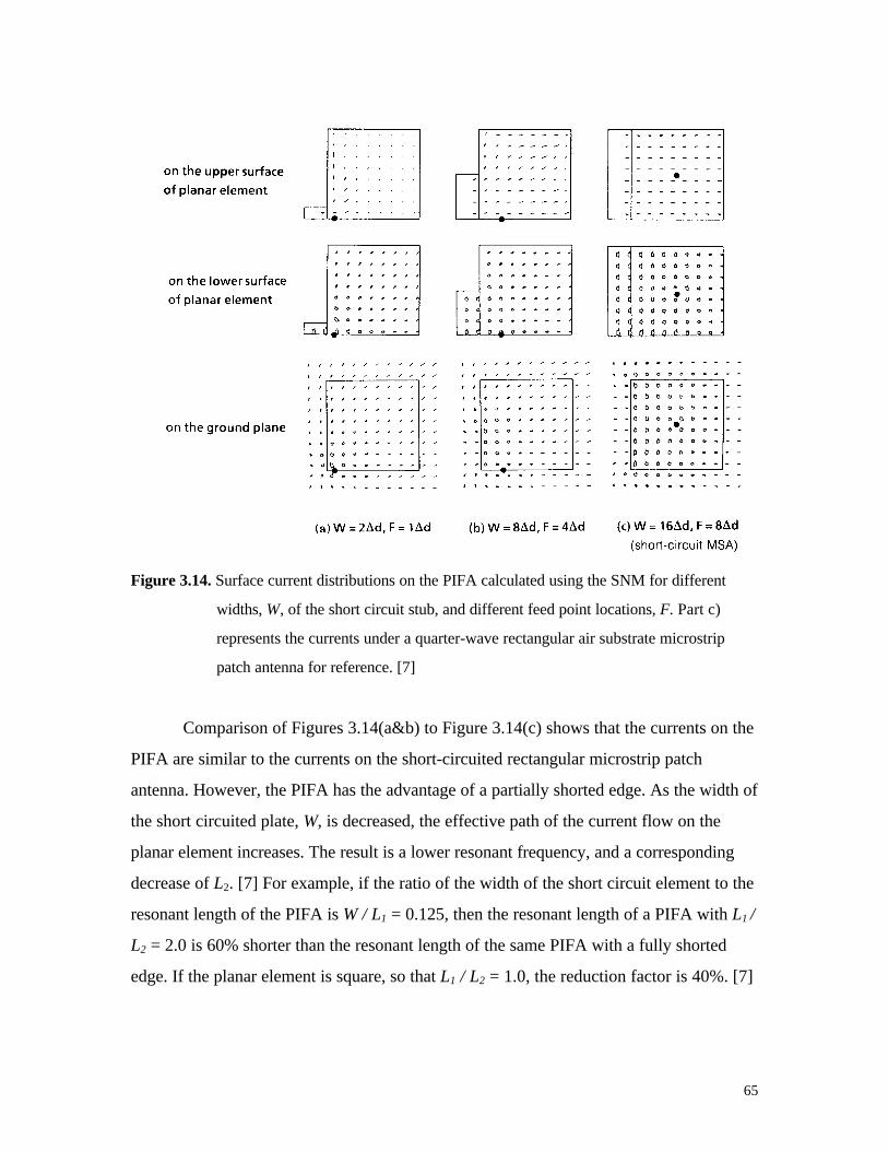
The surface current distributions on a resonant PIFA, modeled using the SNM, are
illustrated in Figure 3.14 for different widths, W, of the short-circuit plate, and feed point
locations, F. In Figure 3.14 the distributions in the top row correspond to the current on
the upper side of the planar element. The distributions in the middle row correspond to the
currents on the lower face of the planar element. The distributions in the bottom row are
the currents that flow back along the ground plane under the planar element. [7] The
currents on the short-circuited plate are shown in all cases, and the feed point is denoted

63
by a filled black circle. The direction of the current is shown using an arrow and the
magnitude of the current is given by the area within the arrow. [7] Figure 3.14 shows that
currents flow out along the lower side of the planar element, and return on the surface of
the ground plane. These currents set up the inner electric and magnetic fields between the
planar element and the ground plane. The currents on the ground plane produce the image
of the PIFA element. [7] The currents on the top face of the planar element are much
smaller than those on the lower face except at the edges of the planar element. The edge
currents on the plate contribute to the fringing fields which are a radiating mechanism of
the PIFA. [7]

64
Figure 3.13. Distribution of the electric fields, Ex, Ey, and Ez in the x-y plane calculated using the
SNM where the observed plane is 2.5∆d above the ground plane for Ez, and 2∆d
above the ground plane for Ex and Ey. [7]
65
Figure 3.14. Surface current distributions on the PIFA calculated using the SNM for different
widths, W, of the short circuit stub, and different feed point locations, F. Part c)
represents the currents under a quarter-wave rectangular air substrate microstrip
patch antenna for reference. [7]
Comparison of Figures 3.14(a&b) to Figure 3.14(c) shows that the currents on the
PIFA are similar to the currents on the short-circuited rectangular microstrip patch
antenna. However, the PIFA has the advantage of a partially shorted edge. As the width of
the short circuited plate, W, is decreased, the effective path of the current flow on the
planar element increases. The result is a lower resonant frequency, and a corresponding
decrease of L2. [7] For example, if the ratio of the width of the short circuit element to the
resonant length of the PIFA is W / L1 = 0.125, then the resonant length of a PIFA with L1 /
L2 = 2.0 is 60% shorter than the resonant length of the same PIFA with a fully shorted
edge. If the planar element is square, so that L1 / L2 = 1.0, the reduction factor is 40%. [7]

66
The resonant frequency of the PIFA depends upon the width of the short circuited
stub, W, the height of the element, h, and the dimensions of the planar element, L1 and L2.
To derive the resonant frequency of the PIFA, a factor, γ1, is calculated that involves the
height, h, and the length of the planar element, L2. This factor is
γ 1 24= +( )L h (3.50)
Another factor, γ2, is calculated that treats the effectively lengthened current path due to
the partial short-circuit. The second factor is
γ 2 1 24= + + −( )L L h W (3.51)
The factors γ1 and γ2 are substituted into one of the following equations to determine the
resonant frequency of the PIFA:
frc r c L
Lr = + − ≤γ γ1 2
1
2
11
( )(3.52)
and
fr c r c L
Lr
k k
= +−
>γ γ1 2
1
2
11
( )(3.53)
where r = W / L, and k = L1 / L2. [7]
The radiation pattern of the IFA and PIFA are the same as that of the ILA if t is
small compared to the length of the horizontal or planar element. The ILA radiation
patterns are in Figure 3.4.
The bandwidth of the PIFA can be improved using a proximity coupled feed. The
proximity coupled feed does not touch the planar element of the PIFA. Instead, the
feedline is coupled capacitively to the planar element of the PIFA using a plate at the end
of the feedline that is oriented parallel to the planar element. The proximity coupled PIFA
is the subject of the next section.

67
3.4.3. Proximity Coupled Planar Inverted-F Antenna
Normally the Planar Inverted-F Antenna (PIFA) is fed coaxially with the shielding
of the feedline connected to the ground plane and the center conductor attached to the
planar element. [2] An alternative to the contacting feed is the proximity coupled feed. In
proximity coupling, the center conductor of the coaxial line is terminated with a plate that
is oriented parallel to the planar element of the PIFA. Figure 3.15 shows a PIFA with a
proximity coupled feed.
Planar Element
Proximity Coupled Feed
Ground Plane
Coaxial Line
Figure 3.15. Planar inverted-F antenna fed using proximity coupling
In Figure 3.15 the plate at the end of the feedline acts as an additional load that stores
charge and makes the current distribution on the feedline more uniform. [1] The proximity
coupled feed adds three degrees of freedom to the impedance matching of the antenna: the
length and width of the feed plate, and the distance between the feed plate and the planar
element. [8] By adjusting these parameters along with the location of the feed, the
proximity coupled PIFA can be impedance matched to a transmission line.
A proximity coupled feed offers a number of advantages. First it is easier to change
the location of the proximity coupled feed with respect to the planar element since there is
not a direct connection. [8] Second, the loading effect of the capacitive feed causes the
proximity fed PIFA to have a lower resonant frequency than a typical PIFA. At resonance,
the planar element of the PIFA has a length, L2, slightly less than λ/4. Using proximity
coupling, L2 can be reduced to λ/8. [8]
Proximity coupling also has disadvantages. Since the feed plate must be oriented
parallel to the planar element and the ground plane, complexity and manufacturing

68
tolerances are added to the design. In addition, currents on both sides of the feed plate
must be modeled to achieve accurate results. Moment Method codes often neglect the
currents on one side of a planar element. Therefore, brute force numerical methods such
as the Finite Difference Time Domain (FDTD) theory are sometimes necessary. [2]
The primary purpose a proximity coupled feed is manipulation of the input
impedance of the PIFA. Increasing the distance between the feed plate and the planar
element reduces the input impedance. [1] A single PIFA element fed using proximity
coupling and optimized for frequency bandwidth experiences a frequency bandwidth of
about 5% of the center frequency. [1]
In [1], further size reduction of the PIFA is achieved by placing a capacitive load
at the end of the planar element opposite the feed, as illustrated in Figure 3.16. [1]
planar elementcapacitive
load
ground plane
feed
short-circuitplate
h
L
L
h
t
f
f
L L
s
W = Width of Planar Element
W = Width of Feed Elementf
Figure 3.16. A planar inverted-F antenna with a capacitive end load
A proximity coupled PIFA like that in Figure 3.16 was built using the dimensions
specified in Table 3.1.
Table 3.1. Dimensions of a proximity fed PIFA with a capacitive end load

69
Quantity Symbol Value Unit
Resonant Frequency fr 1.8 GHz
Width of Planar Element W 10 mm
Length of Planar Element L 10 mm
Element Height h 5 mm
Feed Point t 5 mm
Width of Feed Plate Wf 8 mm
Length of Feed Plate Lf 8 mm
Height of Feed Plate hf 3.5 mm
Load Capacitor Separation s 0.5 mm
Load Capacitor Length LL 4 mm
The antenna specified in Table 3.1 was built and measured. [1] The measured
impedance bandwidth (VSWR < 2 on a 50 Ω feedline) was 4.7 % of the resonant
frequency. The current distribution on the PIFA was not affected by the proximity coupled
feed or the capacitive end load. [1] Therefore, the proximity coupled feed had no effect on
radiation pattern. [1] As the reactance of the load increased, the resonant frequency of the
antenna decreased. Maximum tuning of the resonant frequency was achieved by changing
the plate separation, s, of the load capacitor. The resonant frequency is also affected by
the load capacitor length, LL. [1] A disadvantage of the capacitive end load is increased
input reactance and narrower impedance bandwidth. [1] The proximity coupled feed is
used to tune out the increased reactance, and preserve the impedance bandwidth of the
end loaded PIFA. [1]
Another way to improve the bandwidth of the inverted-F antenna is to add a
parasitic element to the design. The coupled element resonates at a different frequency
than the fed element. Impedance bandwidth is increased if the resonant frequencies of the
two elements are closely spaced. The Dual Inverted-F Antenna (DIFA) is the subject of
the next section. [2]

70
3.4.4. The Dual Inverted-F Antenna
The Dual Inverted-F Antenna (DIFA) in Figure 3.17 is formed by adding a second
inverted-L element to the Inverted-F Antenna (IFA). The second element is parasitic and
is not directly fed. This antenna configuration is frequently referred to as a dual-L antenna.
[2]
Side View
Back View
Top View
L
Lt
h
S
f
c
Figure 3.17. The geometry of the Dual Inverted-F Antenna (DIFA)
In Figure 3.17, the fed element, of length Lf, and the coupled element, of length Lc, are
separated by an offset, S. The coupled element has a different resonant frequency than the
fed element. If the resonant frequencies of the fed and coupled elements are nearly the
same, the impedance bandwidths of the elements blend together. [2] This serves to widen
the overall impedance bandwidth of the PIFA without an increase in element height, h, or
an alternate feeding technique. [2] An experimental DIFA with planar elements as
reported in [2] is shown in Figure 3.18. The dimensions of the antenna are noted in the
figure.

71
Figure 3.18. An experimental Dual Inverted-F Antenna and its dimensions in mm. [2]
The antenna in Figure 3.18 was designed for a center frequency of 900 MHz. The
individual elements were designed at resonant frequencies of 850 and 950 MHz. [2] The
measured impedance of the DIFA in Figure 3.18 is shown in Figure 3.19. The impedance
is expressed in terms of return loss. A return loss of 10 dB corresponds to a VSWR of 2
and a 10% reflection of input power.
Figure 3.19. Measured impedance versus frequency characteristic of DIFA in Figure 3.18. [2]
Figure 3.19 shows a clear dual resonance. The frequency bandwidth of the DIFA below 10
dB return loss is 14.1% of the center frequency, from 0.872 to 1.004 GHz. The factors
that have the greatest effect on the frequency bandwidth are the height of the element, the

72
width and shape of the gap between the planar elements, and the length of the coupled
arm. [2] The radiation patterns of the DIFA are shown in Figure 3.20.
Figure 3.20. Measured radiation patterns of the Dual Inverted-F Antenna in Figure 3.18. [2]
Figure 3.20 shows that the radiation pattern of the DIFA is relatively omni-
directional in the x-y and y-z planes. [2] The high cross-polarization level is a desirable
characteristic in hand-held multi-path environments. [2]
A variation of the DIFA is presented by Liu and Hall in [9]. A rectangular notch is
cut into the corner of the planar element of a PIFA, and another PIFA with a different
resonant frequency is inserted into the empty space. The resulting geometry is illustrated
in Figure 3.21, along with a side view of the antenna mounted on a rectangular conducting
case.
The DIFA in Figure 3.21 is fed in two locations. The result is a configuration that
is switchable between the 900 MHz cellular band, and the 1800 MHz PCS band. [9] The
volume occupied by the antenna is almost identical to that of a PIFA designed at 900
MHz. [9] Spurious radiation and a loss of radiation efficiency occurs if there is mutual
coupling occurs between the elements of a dual band antenna. Mutual coupling between
the elements of the DIFA in Figure 3.21 is below -17 dB at both resonant frequencies. [9]

73
The input impedance of the antenna is illustrated in Figure 3.22 for both resonant
frequencies in terms of return loss.
Figure 3.21. Geometry and dimensions of a dual-band DIFA. [9]
Figure 3.22. Modeled and empirical impedance data for the dual-band DIFA in Figure 3.21. [9]

74
Figure 3.22 shows that the antenna is well matched to a 50 Ω coaxial line at both resonant
frequencies. The frequency bandwidth of the antenna at 0.9 GHz is 63 MHz, or 7% of the
resonant frequency. At 1.76 GHz, the frequency bandwidth of the antenna is 110 MHz, or
6.25% of the center frequency. [9] The radiation patterns of the dual-band DIFA are
illustrated in Figure 3.23.
Figure 3.23. Radiation patterns of the dual-band DIFA in Figure 3.21, modeled using the FDTD
technique in the x-y plane at (a) 1.76 GHz and (b) 1.9 GHz. [9]
The radiation patterns illustrated in Figure 3.23 show that the Eφ field of the dual-
band DIFA is omni-directional in the x-y plane at both resonant frequencies. This is a
desirable feature for hand-held applications. [9]
The DIFA has a number of features that are attractive for hand-held applications.
It is low-profile, relatively compact, has a wide frequency bandwidth and omni-directional
coverage in azimuth. It exhibits good performance on a conducting box of finite
dimensions and lends itself to dual-banding. Thus, the DIFA is an excellent candidate for
use in the hand-held environment.

75
3.5. Conclusion
In this chapter, the Inverted-L Antenna (ILA) and a number of its variations were
presented. The variations on the ILA included the Inverted-F Antenna (IFA), the Planar
Inverted-F Antenna (PIFA) and the Dual Inverted-F Antenna (DIFA). The variations on
the ILA are summarized in Table 3.2.
Table 3.2. Summary of variations on the Inverted-L Antenna
Name Figure
Containing
Geometry
Critical
Dimensions
Typical
Bandwidth
(% fresonant)
Azimuthal
Coverage
Inverted-F
Antenna (IFA)
3.10 h ≈ λ / 16
L ≈ λ / 4
< 2 % omni
Planar Inverted-F
Antenna (PIFA)
3.12 h ≈ λ / 16
L < λ / 4
W varies
5 %
omni
Dual Inverted-F
Antenna (DIFA)
3.17 h ≈ λ / 16
Lfed ≈ λ / 4
Lcoupled ≠ Lfed
14 % possible
5-7 % per dual
banded frequency
omni
The ILA variations experience higher input resistance at resonance, and wider
impedance bandwidth than the ILA. The antenna with the widest impedance bandwidth is
the DIFA. In addition, the DIFA is as compact as the PIFA and matches the ILA, IFA,
and PIFA in height reduction. The DIFA provides omni-directional coverage, good
performance on size-constrained ground planes, and lends itself to dual-banding. This
makes the DIFA ideal for hand-held applications.
In the next chapter the DIFA is studied in further detail. A numerical model of the
DIFA is developed using the Method of Moments (MoM). This model is implemented and
the results are compared to empirical measurements. The performance of the DIFA is

76
compared to that of the IFA over an infinite ground plane and over conducting boxes of
various finite dimensions.
REFERENCES FOR CHAPTER 3
1. Rowell, C. B., Murch, R. D., “A Capacitively Loaded PIFA for Compact PCS Handsets”. IEEEAntennas and Propagation Society Symposium Digest, Baltimore, July 1996, pp. 742-745.
2. Jensen, M. A., Rahmat-Samii, Y., “FDTD Analysis of PIFA Diversity Antennas on a Hand-HeldTransceiver Unit”. IEEE Antennas and Propagation Symposium Digest, July 1993, pp. 814-817.
3. Virga, K., Rahmat-Samii, Y., “An Enhanced Bandwidth Integrated Dual-L Antenna for MobileCommunication Systems - Design and Measurement”. IEEE Antennas and Propagation SocietyInternational Symposium, Newport Beach, CA, 1995.
4. Fujimoto, K., Henderson, A., Hirasawa, K., James, J.R. Small Antennas, Research Studies Press Ltd.,London and John Wiley & Sons Inc., New York, 1987. Section 2.4.1.
5. Stutzman, W. L., Thiele, G. A. Antenna Theory and Design. John Wiley and Sons, New York, 1981.
6. Wunsch, D.A. “A Closed-Form Expression for the Driving Point Impedance of the Small Inverted-LAntenna”. IEEE Transactions on Antennas and Propagation, v. 44, n. 2, Feb. 1996.
7. Hirasawa, K., Haneishi, M. (eds.), Analysis, Design, and Measurement of Small and Low-ProfileAntennas. Chapter 5: Taga, T. “Analysis of Planar Inverted-F Antennas and Antenna Design forPortable Radio Equipment”. Artech House, Boston, 1992.
8. Kagoshima, K., Tsunekawa, K, Ando, A., “Analysis of a Planar Inverted-F Antenna Fed by EMCoupling”. IEEE Antennas and Propagation Society International Symposium, Chicago, IL,1992, pp. 1702-1705.
9. Liu, Z., Hall P.S. “A Novel Dual-Band Antenna for Hand-Held Portable Telephones”. IEEE Antennasand Propagation Society International Symposium, July 1996, pp. 54-57.