Embed Size (px)
Citation preview

Chapter 4: Asymmetrical Pulse Width Modulation Control
108
Chapter 4
Asymmetrical Pulse Width Modulation Control
The output current of Type-II RICs is theoretically constant irrespective of
changes in the load resistance, for constant input dc voltage. As examined
experimentally in the previous chapter, the output current of practical circuits droops
slightly with the output power, even with the constant input dc voltage, because of
increasing drops in various circuit elements. Moreover, input dc voltage in most of the
practical off-line applications itself is unregulated when it is conveniently obtained by
rectifying the ac main voltage using diode rectifier and smoothened using passive
filter. Therefore, for practical application of Type-II RIC as a current-source power
supply, it is necessary to regulate the output current, particularly against the input
voltage variations. Some applications also demand that it should be possible to set and
regulate the output current from near-zero to the maximum rated value.
Since Type-II RICs behave as a current-source only when it is operated at a
particular frequency, the method using variation of switching frequency can not be
applied to control the output. The output current can be regulated and varied over a
wide range by either varying the input dc voltage using another converter in the front-
end or using fixed-frequency control methods. In the former case, two cascaded
converters reduce overall conversion efficiency, increase complexity, component
count and cost.
Chapter 4: Asymmetrical Pulse Width Modulation Control
109
The CM or PSPWM control [119] – [132] and asymmetrical pulse-width-
modulation (APWM) control [136] – [139] are the two common fixed-frequency
PWM control strategies. The CM control can be applied only with the full-bridge
converter whereas APWM control can be used with half-bridge as well as full-bridge
converter. While APWM control leads to asymmetric operation of the high-side and
the low-side switches and leads to unequal voltages across the leg capacitors, it has
been popularly applied to power converters (resonant as well as non-resonant) due to
simpler implementation and soft-switching. Moreover, half-bridge topology has a
relatively simpler structure, less number of switches with associated driving circuits
and has been a popular approach for low- and medium-power level applications. For
these reasons, this chapter examines the possibility of using APWM control to Type-
II RICs, exemplified using LCL-T RC.
4.1 APWM Controlled LCL-T RC
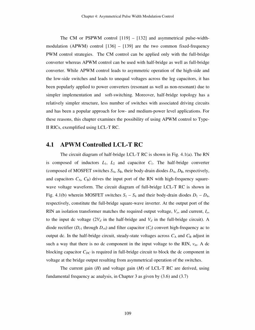
The circuit diagram of half-bridge LCL-T RC is shown in Fig. 4.1(a). The RN
is composed of inductors L1, L2 and capacitor C1. The half-bridge converter
(composed of MOSFET switches SA, SB, their body-drain diodes DA, DB, respectively,
and capacitors CA, CB) drives the input port of the RN with high-frequency square-
wave voltage waveform. The circuit diagram of full-bridge LCL-T RC is shown in
Fig. 4.1(b) wherein MOSFET switches S1 – S4 and their body-drain diodes D1 – D4,
respectively, constitute the full-bridge square-wave inverter. At the output port of the
RIN an isolation transformer matches the required output voltage, Vo, and current, Io,
to the input dc voltage (2Vd in the half-bridge and Vd in the full-bridge circuit). A
diode rectifier (Dr1 through Dr4) and filter capacitor (Cf) convert high-frequency ac to
output dc. In the half-bridge circuit, steady-state voltages across CA and CB adjust in
such a way that there is no dc component in the input voltage to the RIN, vin. A dc
blocking capacitor CDC is required in full-bridge circuit to block the dc component in
voltage at the bridge output resulting from asymmetrical operation of the switches.
The current gain (H) and voltage gain (M) of LCL-T RC are derived, using
fundamental frequency ac analysis, in Chapter 3 as given by (3.6) and (3.7)
Chapter 4: Asymmetrical Pulse Width Modulation Control
110
CB
L1
L2
C1
2Vd
Cf
Tr
RL
SA
SB
vin v
c1
iL1 i
L2+ +
- -
CA
Dr1
Dr2
Dr3
Dr4
DB
DA
Io
Vo
+
-
1:n
(a)
Vd
Cf
Tr
RL
S3
S4
vin
+ +
- -
Dr1
Dr2
Dr3
Dr4
D4
D3
Io
Vo
+
-
S1
S2
D1
D2
L1
L2
iL2
iL1
vc1
1:n
C1
CDC
(b)
Fig. 4.1: Circuit diagrams of (a) half-bridge and (b) full-bridge LCL-T RC.
respectively and it is shown that the H is independent of load only if the converter is
operated at 1=nω , given by (3.8). Therefore, the method using variation of switching
frequency to control the output can not be applied - or else current source behaviour
will be lost. Besides, the plots of Fig. 3.2(a) show that H is relatively flat in the
vicinity of the operating point 1=nω . Thus, the variation of switching frequency will
not provide wide conversion range and regulation against large input voltage
variations. Therefore fixed-frequency control should be used. Additionally, if γ =1, vin
and iL1 are in phase resulting in the lowest conduction loss in the switches. Therefore,
for the subsequent analysis of LCL-T RC with APWM control, it is assumed that the
converter operates at 1=nω and γ =1.
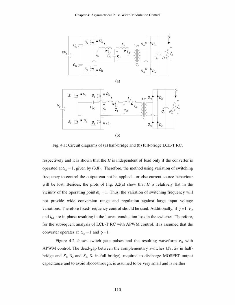
Figure 4.2 shows switch gate pulses and the resulting waveform vin with
APWM control. The dead-gap between the complementary switches (SA, SB in half-
bridge and S1, S2 and S3, S4 in full-bridge), required to discharge MOSFET output
capacitance and to avoid shoot-through, is assumed to be very small and is neither

Chapter 4: Asymmetrical Pulse Width Modulation Control
111
t
t
t
SA (S1,S4)
SB (S2,S3)
vin
2Vd (1-D)
-2Vd D
Ts
DTs
Fig. 4.2: Idealized waveforms of gate pulses for the switches and vin with APWM
control. The switches mentioned in the bracket correspond to the full-bridge
converter.
explicitly shown in Fig. 4.2 nor considered in the analysis. Amplitude of the
fundamental component of vin can be derived as,
( )DV
V d
in ππ
sin4
1 = (4.1)
where D is the duty-cycle defined in Fig. 4.2. Thus Vin1 can be controlled from zero to
its maximum value by changing D. Assuming that the power is transferred to the
output only by the fundamental component of source excitation, H and M with
APWM control can be approximated as,
( )DHn
ππω
sin8
21=
= (4.2)
( )DQ
Mn
ππω
sin18
21=
= (4.3)
4.2 State-Space Model and Modes of Operation
An equivalent circuit diagram of LCL-T RC is shown in Fig. 4.3 for the state-
space analysis. The input bridge is represented by a square-wave voltage source vin
which can be expressed in the steady-state for the pth
cycle of operation as,

Chapter 4: Asymmetrical Pulse Width Modulation Control
112
L1=L L
2=L
C1=C v
c
iL1
iL2
+
-
vin
vo
+
-
+
-
Fig. 4.3: Equivalent circuit diagram of LCL-T RC.
( )DVv din −= 12 for ( ) ss TpDtpT 1+<< and
DVv din 2−= for ( ) ( ) ss TptTpD 11 +<<+ (4.4)
wherein Ts is the time period of one cycle. Output filter capacitor, Cf, is assumed to be
large enough so as to result in a very low ripple in the output voltage even with large
values of Q. Under near no-load conditions where RL tends to zero (that is, Q tends to
infinity) this assumption breaks down as the ripple becomes significant. Since Cf in a
practical power converter would be chosen to yield an acceptably low output voltage
ripple down to typically 5 % of full-load condition (corresponding to a value of Q to
be 20 times its full-load value) and since, as discussed subsequently, salient operating
modes occur at lower values of Q, the aforementioned simplifying assumption is valid
in the regions of interest. Therefore the transformer, rectifier and filter on the output
side of the RN are represented in Fig. 4.3 by the square-wave voltage vo which can be
expressed as,
n
Vv o
o = for 02
>Li and
n
Vv o
o −= for 02
<Li
(4.5)
Choosing the inductor currents iL1, iL2 and capacitor voltage vc as the state variables,
the state-space model is derived as,
×
−
+
×
−
−
=
−
−
−
−
−−
o
in
L
L
c
L
L
c
v
v
L
L
i
i
v
L
L
CC
i
i
v
dt
d
1
1
1
1
11
0
0
00
00
00
0
2
1
2
1 (4.6)
The differential equations in (4.6) are numerically solved for the sources described by
(4.4) and (4.5) to obtain steady-state waveforms of the state variables. It is observed
Chapter 4: Asymmetrical Pulse Width Modulation Control
113
that the circuit can have four operating modes depending on the steady-state
waveforms of vin and iL1, which, in turn, depend on D and Q. Each mode of operation
is characterized by the different circuit waveforms representing different device
conduction sequence, thereby creating different conditions during the device
switching. The converter’s operation in different modes is described for the half-
bridge converter [Fig. 4.1(a)] in the following paragraphs. However, the conducting
devices during various sub-intervals in full-bridge circuit [Fig. 4.1(b)] are also marked
inside the respective figures for the completeness.
4.2.1 Mode-I
Steady-state waveforms of vin and iL1 in these modes of operation are shown in
Fig. 4.4. This mode of operation mainly occurs when D≈0.5. Before t=to, switch SB
was conducting. At t=to, SB is turned off and gate pulse is applied to SA. Since iL1 is
negative at this instant, it flows through DA. At t=t1, DA turns off naturally at zero
current and iL1 now flows through SA. Similarly in the next half cycle, SA is turned off
at t=t2 and gate pulse is applied to SB. Since iL1 is positive at this instant, flows
through DB. At t=t3, DB turns off naturally at zero current and iL1 flows through SB. At
t=t4, SB is turned off and SA is turned on once again marking the beginning of the next
cycle. Thus in this mode, the device conduction sequence is such that the
φ
t
t4
iL1
vin
DA( D
1,D
4 )
DB( D
2,D
3 )
SB( S
2,S
3 )S
A( S
1,S
4 )
t3t
1t2
t0
Fig. 4.4: Steady-state waveforms of vin and iL1 in Mode-I operation.

Chapter 4: Asymmetrical Pulse Width Modulation Control
114
anti-parallel diodes conduct prior to the switch conduction resulting in ZVS turn-on
for both the switches.
4.2.2 Mode-II
Steady-state waveforms of vin and iL1 in this mode of operation are shown in
Fig. 4.5. This mode of operation can also occur when D≈0.5. Before t=to, diode DB
was conducting. At t=to gate pulse is applied to SA. Diode DB turns off and iL1 flows
through SA. At t=t1, iL1 reverses its direction and becomes negative. SA turns off at zero
current and iL1 is transferred to DA until t=t2 when gate pulse is applied to SB. At this
instant, diode DA turns off and iL1 is carried by SB. At t=t3, SB is turned off naturally
with zero current as iL1 reverses its direction and starts flowing through DB. At t=t4, SA
is turned on once again marking the beginning of the next cycle. Thus in this mode,
the device conduction sequence is such that the anti-parallel diodes conduct after the
switch conduction resulting in ZCS turn-off for both the switches.
4.2.3 Mode-III
Steady-state waveforms of vin and iL1 in this mode of operation are shown in
Fig. 4.6. Similar to Mode-I, the device conduction sequence in this mode results in
φ
t
iL1
vin
DA( D
1,D
4 ) D
B( D
2,D
3 )
SB( S
2,S
3 )S
A( S
1,S
4 )
t4
t3t
1t2
t0
Fig. 4.5: Steady-state waveforms of vin and iL1 in Mode-II operation.
Chapter 4: Asymmetrical Pulse Width Modulation Control
115
t
SB( S
2,S
3 )
DB( D
2,D
3 )
DA( D
1,D
4 )
( D2,D
3 )( S
1,S
4 )
t3b
t3a
iL1
vin
DB
SB( S
2,S
3 )
SA
t4
t3
t1
t2
t0
Fig. 4.6: Steady-state waveforms of vin and iL1 in Mode-III operation.
ZVS turn-on of all the switches. The difference is that, iL1 oscillates across zero twice
during the time interval between t=t2 and t=t4 causing SB and DB to conduct twice
during this interval. At t=t2, SA is turned off and gate pulse is applied to SB. Since iL1 is
positive at this instant, it flows through DB until t=t3 when it reverses and starts
flowing through SB. Current iL1 reverses its direction at t=t3a causing DB to conduct
and once again at t=t3b causing SB to conduct. The additional commutations of SB and
DB in this mode of operation are ideally loss-less since they occur under zero current
and zero voltage condition. At t=t4, SA is turned on once again marking the beginning
of the next cycle.
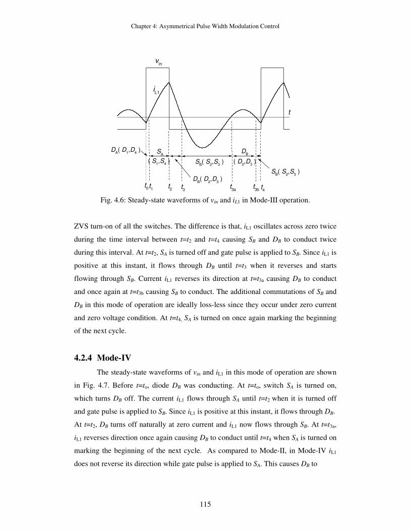
4.2.4 Mode-IV
The steady-state waveforms of vin and iL1 in this mode of operation are shown
in Fig. 4.7. Before t=to, diode DB was conducting. At t=to, switch SA is turned on,
which turns DB off. The current iL1 flows through SA until t=t2 when it is turned off
and gate pulse is applied to SB. Since iL1 is positive at this instant, it flows through DB.
At t=t2, DB turns off naturally at zero current and iL1 now flows through SB. At t=t3a,
iL1 reverses direction once again causing DB to conduct until t=t4 when SA is turned on
marking the beginning of the next cycle. As compared to Mode-II, in Mode-IV iL1
does not reverse its direction while gate pulse is applied to SA. This causes DB to

Chapter 4: Asymmetrical Pulse Width Modulation Control
116
t
DB( D
2,D
3 )
( D2,D
3 )
SA( S
1,S
4 )
iL1
vin
DB
SB( S
2,S
3 )
t4
t3a
t2 t
3t0
Fig. 4.7: Steady-state waveforms of vin and iL1 in Mode-IV operation.
conduct twice during the time interval t=t2 to t=t4. Also, diode DA never conducts in
this mode. Observe that DB conducts prior to the conduction of SB, resulting in ZVS
turn-on condition for SB. However, SA operates under hard-switching condition.
4.2.5 Discussion
The waveforms of vin and iL1 in different operating modes shown in Fig. 4.4 to
Fig. 4.7 along with the marked conducting devices during various sub-intervals enable
the identification of conditions experienced by various switches and diodes during
switching. This, in turn, enables the identification of desired operating modes, in
which switches and diodes operate under the most favourable switching conditions.
Table 4.1 summarizes the switching conditions for the switches and diodes in the four
operating modes described above. In Mode-I and Mode-III, anti-parallel diode of each
switch conducts prior to the conduction of the switch resulting in ZVS turn-on. Turn-
on snubbers are eliminated. Slower anti-parallel diodes and loss-less capacitor turn-
off snubber can be used. Body-drain diode and output capacitance of power MOSFET
can therefore be used reducing component count. In Mode-II, all the switches are
turned off at zero current. However, when a switch is turned on the anti-parallel diode
of the other switch in the leg is conducting. Therefore, fast anti- parallel diodes and
lossy (or complicated energy recovery) turn-on snubbers are required. Body-drain

Chapter 4: Asymmetrical Pulse Width Modulation Control
117
Table 4.1: Switching conditions for the switches and diodes in half-bridge LCL-T RC
in various operation modes with APWM control.
Switch SA Switch SB Diode DA Diode DB Mode
turn-on turn-off turn-on turn-off turn-on turn-off turn-on turn-off
I ZV, ZC FV, FC#
ZV, ZC FV, FC#
FV, FC# ZV, ZC FV, FC
# ZV, ZC
II FV, FC ZV, ZC FV, FC ZV, ZC ZV, ZC FV, FC ZV, ZC FV, FC
III ZV, ZC FV, FC#
ZV, ZC FV, FC#
FV, FC# ZV, ZC
FV, FC# (t2- t3)
ZV, ZC (t3a- t3b)
ZV, ZC (t2- t3)
ZV, ZC (t3a- t3b)
IV FV, FC FV, FC ZV, ZC ZV, ZC
NC NC FV, FC (t2- t3)
ZV, ZC (t3a- t4)
ZV, ZC (t2- t3)
FV, FC (t3a- t4)
ZV: zero-voltage, ZC: Zero-current, FV: Finite voltage, FC: Finite current, NC: No conduction #: Loss-less capacitor turn-off snubber can be used to reduce rate of rise of voltage and switching loss during
switch turn-off.
diode of MOSFET cannot be used. Additionally, the switches carry diode reverse-
recovery current and the discharge current of MOSFET output capacitance at turn-on,
causing more losses. In Mode-IV, switch SB operates with favourable switching
conditions since DB conducts prior to its conduction. However, SA operates with hard-
switching condition.
4.3 Mode Boundaries
The above discussion suggests that Mode-I and Mode-III are the preferred
modes of operation as ZVS of all the switches is achieved apart from the other
mentioned advantages. It is therefore important to determine the boundaries between
the transitions of converter’s operation from one mode into another and define the
operating regions. The waveforms of vin and iL1 in the steady state as the converter
makes transition from one mode into another are shown in Fig. 4.8.
Since the steady-state waveforms of vin and iL1 depend on two parameters, D
and Q, the regions of different modes of operation of the converter can be
conveniently defined on, what is called here, the D-Q plane. Figure 4.9 shows the D-
Q plane of APWM controlled LCL-T RC at 1=nω and γ =1 explicitly showing the
regions of converter’s operation in various modes. The following important
observations are made:
1. If the converter is designed in such a way that the value of Q at full-load
condition is greater than 1.07, then the converter can operate only in Mode-I

Chapter 4: Asymmetrical Pulse Width Modulation Control
118
t
iL1v
in
t
iL1
vin
(a) (b)
t
iL1
vin
t
iL1
vin
(c) (d)
Fig. 4.8: Waveforms of vin and iL1 in steady-state as the converter makes transition
from one mode into another. Boundary between (a) Mode-I and Mode-IV, (b) Mode-
II and Mode-IV, (c) Mode-III and Mode-IV and (d) Mode-I and Mode-III.
or Mode-III for all the values of D in the range 0 to 0.5 and down to the no-
load operation.
2. Under the symmetrical input voltage waveform (that is, D=0.5), it is seen from
the D-Q plane and the description of various operating modes, that iL1 lags vin
for Q>0.81 whereas iL1 leads vin for Q<0.81. This behaviour is not predicted
by the fundamental frequency ac analysis, which suggests that iL1 and vin are
always in phase. Figure 4.10 shows the variation of phase angle ( )φ between
iL1 and vin for operation at D=0.5. A positive value of φ means iL1 is leading
vin, and vice versa.

Chapter 4: Asymmetrical Pulse Width Modulation Control
119
0 1 2 3 4 5 60.0
0.1
0.2
0.3
0.4
0.5
Q=0.81
Q=1.07
Mode-IV
Mode-II
Mode-III
Mode-I
D
Q
Fig. 4.9: D-Q plane of APWM controlled LCL-T RC showing the regions of different
modes of operation.
0 1 2 3 4 5-20
-10
0
10
20
30
φ 0
Q
Fig. 4.10: Variation of φ as a function of Q for operation at D=0.5 in APWM
controlled LCL-T RC.

Chapter 4: Asymmetrical Pulse Width Modulation Control
120
0 1 2 3 4 5 60.0
0.1
0.2
0.3
0.4
0.5
ZVS
ZVS
D
Q
Fig. 4.11: Regions of ZVS operation of all the switches in LCL-T RC with APWM
(solid line) and CM control (broken line).
CM control is another widely used fixed-frequency PWM control method. The
state-space model described by (4.6) was also solved numerically under CM control
to identify the region of ZVS operation of all the switches on the D-Q plane. Figure
4.11 compares the regions of ZVS operation of LCL-T RC with APWM and CM
control. ZVS operation of all the switches is possible in the region to the right side of
the boundary. APWM control is observed to allow ZVS operation in the entire range
of D (0 to 0.5) over a wider range of Q than the CM control. Since CM control does
not offer any advantage over APWM control in this regard, it is not studied and
characterized any further.
4.4 Converter Design
For the design of LCL-T RC CC power supply the design specifications are:
minimum and maximum value of input dc voltage (Vd,min and Vd,max, respectively),
maximum output current (Io,max), maximum load resistance (RL,max) corresponding to
the full-load condition and switching frequency (fs). The full-load Q (QFL) can be
written as,
Chapter 4: Asymmetrical Pulse Width Modulation Control
121
max,
2
max,
1o
2
L
n
L
FLR
Zn
R
LnQ ==
ω (4.7)
The expression for n, L1, L2 and C1 are derived in terms of converter’s terminal
parameters as follows:
( )maxmin,
max,max,2
sin8 DV
QRIn
d
FLLo
π
π= (4.8)
( )
sFLLo
d
fQRI
DVLL
max,
2
max,
max
22
min,
521
sin32 π
π== (4.9)
( )sd
FLLo
fDV
QRIC
max
22
min,
max,
2
max,3
sin128 π
π= (4.10)
The design of the converter is thus governed by the selection of QFL. The
value of QFL is shown to have direct effect on the size of the reactive components,
judged by the kVA/kW rating of the RIN (see Fig. 3.3). Additionally, the choice of QFL
also governs the operation of converter in different modes with APWM control as
described in the previous sections.
It can be observed from the D-Q plane of Fig. 4.9 that if the converter is
designed in such a way that the value of QFL is greater than 1.07, then the converter
can operate only in Mode-I or Mode-III for all the values of D in the range 0 to 0.5
and down to the no-load operation. In this way, the operation in Mode-II or Mode-IV
can be avoided and ZVS operation of all the switches is ensured. However, this choice
of QFL is different than the optimum value of QFL=Qopt=0.81. The kVA/kW rating of
the resonant tank first decreases as Q is increased, reaches minimum value at Q=Qopt
and then again increases as Q is increased further (see Fig. 3.3). However, the
increase in kVA/kW rating with increase in Q above Q=Qopt is not as steep as the fall
in kVA/kW rating with increase in Q below Q=Qopt. Therefore, increasing Q slightly
from Qopt does not result in large penalty in terms of size. Further, φ also does not
increase significantly with increase in Q (see Fig. 4.10). Therefore for the same output
power, iL1 also does not increase significantly. Thus the converter design with QFL >
1.07 does not significantly increase the size of the RIN and losses in semiconductors
and it ensures ZVS operation of all the switches over the entire range of operation.

Chapter 4: Asymmetrical Pulse Width Modulation Control
122
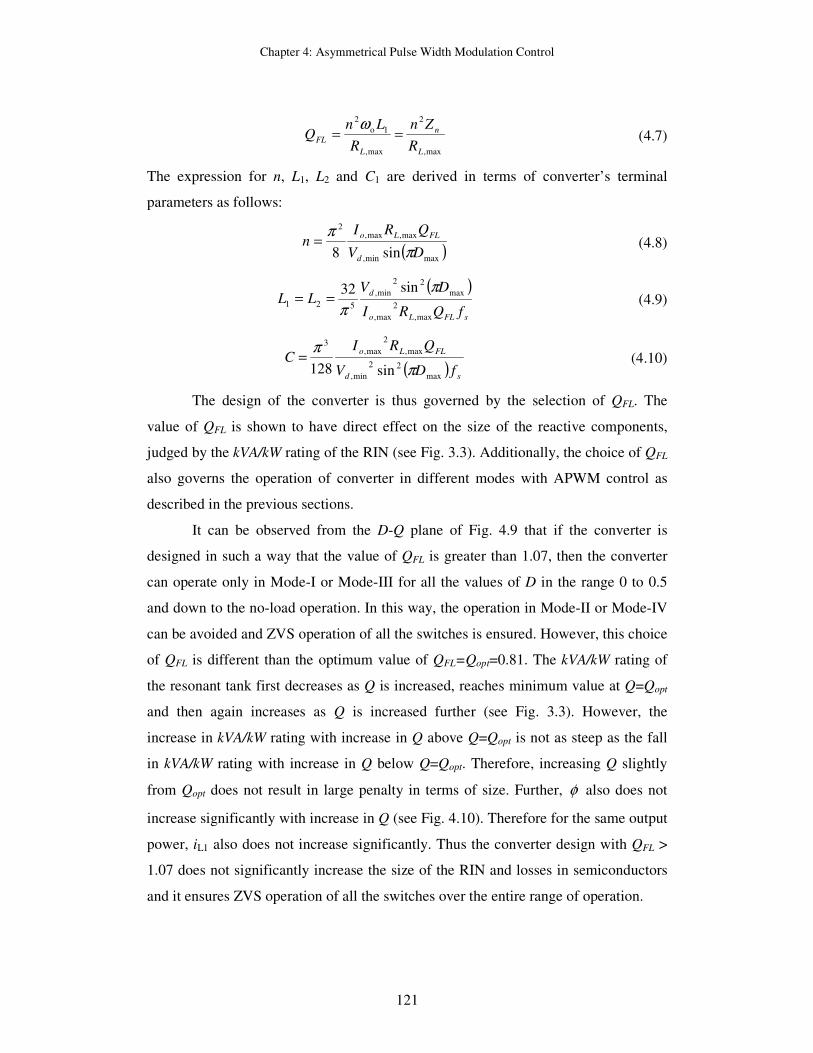
4.5 Experimental Results
A prototype half-bridge 500 W, 100 kHz converter is designed and built. The
specifications and design values of the major components of the converter are
summarized in Table 4.2. QFL=1.2 is chosen in order to have full-range ZVS operation
of the switches. The Table also lists, inside the brackets, the values of the components
actually used in the prototypes, which are adjusted to nearest available or realizable
value. IRF 840 MOSFETs are used as the switches in the half-bridge converter. Fast-
recovery diodes MUR 4100 are used for the output bridge rectifier. A 10 µF capacitor
forms the output filter in the prototype.
The experimental waveforms of vin and iL1 demonstrating the different modes
of operation are shown in Fig. 4.12. The converter was made to operate in these
modes by using different combinations of D and Q, the latter being adjusted by
changing the load resistance. Note that to demonstrate the converter’s operation in
Mode-II and Mode-IV, RL was purposefully made higher (2000 Ω and 1000 Ω,
respectively) than RL,max (500 Ω), thereby overloading the converter. Therefore, the
waveforms of Fig. 4.12 are captured with reduced input dc voltage (50 V). The
voltage waveforms in Fig. 4.12 can be observed to be cleaner in Mode-I and Mode-III
Table 4.2: Specifications and design parameters of the prototype APWM controlled
LCL-T RC. The respective values actually used in the prototypes are given in the
brackets.
Parameter Value
Design specifications
2Vd (V) 300
Io,max (A) 1
RL,max (Ω) 500
Dmax 0.5
fs (kHz) 100
Calculated component values
QFL 1.2
N1/N2 0.2025 (0.2)
C (nF) 64.72 (66)
L1, L2 (µH) 39.18 (38.02)
fs (kHz) 100
Chapter 4: Asymmetrical Pulse Width Modulation Control
123
(a) (b)
(c) (d)
Fig. 4.12: Experimental waveforms of vin [trace (1), 20 V/div] and iL1 [trace (2), 0.5
A/div in (a), (c) and 1 A/div in (b), (d)] in APWM controlled LCL-T RC (a) Mode-I
(D=0.5, Q=1.2), (b) Mode-II (D=0.5, Q=0.3), (c) Mode-III (D=0.2, Q=1.2) and (d)
Mode-IV (D=0.4, Q=0.6). X-scale: 2.5 µs/div.
due to soft-switching. Figure 4.13 demonstrates converter’s operation in the desired
Mode–I and Mode–III at Q=1.2 with full input dc voltage (300 V).
Open-loop control characteristic of the experimental prototype at no-load
(RL~0 Ω) and full-load (RL=500 Ω) is obtained by measuring output current at
different values of D. As shown in Fig. 4.14, the control characteristics is observed to
closely match with the theoretical curve and the output current is seen to be nearly

Chapter 4: Asymmetrical Pulse Width Modulation Control
124
(a) (b)
Fig. 4.13: Experimental waveforms of vin [trace (1), 100 V/div] and iL1 [trace (2), 5
A/div] at Q=1.2. (a) Mode-I (D=0.5) and (b) Mode-III (D=0.2). X-scale: 2.5 µs/div.
0.0 0.1 0.2 0.3 0.4 0.50.0
0.2
0.4
0.6
0.8
1.0
1.2
RL = 500 Ω
RL ~ 0 Ω
Theory
I 0 (
A)
D
Fig. 4.14: Open-loop control characteristics of prototype APWM controlled LCL-T
RC.
independent of load resistance (except for a small increase owing to the decrease in
circuit drops from full-load to no-load) at all values of D.
The conversion efficiency of the prototype is measured by varying D to
change the output power under different loading conditions at 300 V input dc voltage.
Plots of experimental efficiency as a function of the output power are shown in Fig.
4.15. The full-load conversion efficiency of the prototype is measured to be 0.94 and
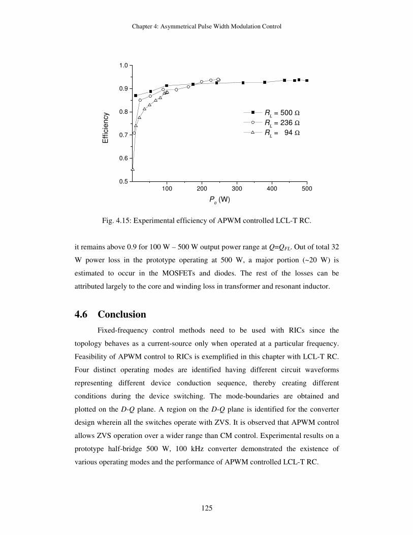
Chapter 4: Asymmetrical Pulse Width Modulation Control
125
100 200 300 400 5000.5
0.6
0.7
0.8
0.9
1.0
RL = 500 Ω
RL = 236 Ω
RL = 94 Ω
Eff
icie
ncy
Po (W)
Fig. 4.15: Experimental efficiency of APWM controlled LCL-T RC.
it remains above 0.9 for 100 W – 500 W output power range at Q=QFL. Out of total 32
W power loss in the prototype operating at 500 W, a major portion (~20 W) is
estimated to occur in the MOSFETs and diodes. The rest of the losses can be
attributed largely to the core and winding loss in transformer and resonant inductor.
4.6 Conclusion
Fixed-frequency control methods need to be used with RICs since the
topology behaves as a current-source only when operated at a particular frequency.
Feasibility of APWM control to RICs is exemplified in this chapter with LCL-T RC.
Four distinct operating modes are identified having different circuit waveforms
representing different device conduction sequence, thereby creating different
conditions during the device switching. The mode-boundaries are obtained and
plotted on the D-Q plane. A region on the D-Q plane is identified for the converter
design wherein all the switches operate with ZVS. It is observed that APWM control
allows ZVS operation over a wider range than CM control. Experimental results on a
prototype half-bridge 500 W, 100 kHz converter demonstrated the existence of
various operating modes and the performance of APWM controlled LCL-T RC.