Embed Size (px)
Citation preview

52
CHAPTER 4
DUAL LOOP SELF BIASED PLL
The traditional self biased PLL is modified into a dual loop
architecture based on the principle widely applied in clock and data recovery
circuits proposed by Seema Butala Anand et al (2001). This modification of
dual loop PLL architecture was attempted mainly to minimize the high gain of
VCO and address the jitter constraints of the traditional self biased PLL in
multi core processor. The narrow capture range resulting from the
incorporated low gain VCO is widened by an additional FLL loop in the
system. The FLL system is configured in such a way that the capture
transients present in the traditional self biased PLL are minimized and
frequency acquisition time is minimized.
The architecture of the modified dual loop PLL is first described.
The loop parameters of the modified dual loop PLL are derived next and the
incorporation of the salient features of the traditional self biased PLL are
discussed. The order of jitter reduction obtained by reducing the VCO gain of
jitter optimized traditional self biased PLL is explained through simulation
results. The optimal choice of low gain VCO that was incorporated in the PLL
of dual loop is discussed. The simulation results of the dual loop system are
presented and the performance is analyzed by comparing with the results of
traditional self biased PLL and with recently reported dual loop PLL.

53
4.1 DUAL LOOP PLL SYSTEM DESCRIPTION
The VCO of the traditional self biased PLL is modified so as to
accept two control inputs. One of the control inputs has a large conversion
gain (coarse), provides wide tuning range, and will form part of the Frequency
Lock Loop (FLL). The other control input has a low conversion gain (fine)
and will form part of the PLL. The loop constituting the FLL is shown in
Figure 4.1 that comprises of a Quadri-correlator based Frequency Detector
(FD), two charge pumps CP1 and CP2, and a bias generator BG1. The charge
pump block CP2 in the FLL is used to emulate the resistance in LPF to make
the bandwidth of the FLL adaptive similar to the technique implemented in
PLL proposed by John Maneatis G.(1996). The task of the FLL is to acquire
and bring the output frequency to within the PLL’s capture range. While the
FLL tracks the reference frequency, the PLL is disabled by a digital control
circuit, and is later enabled when the frequency falls within its capture range.
The FD in the FLL becomes inactive when the frequency difference is within
the PLL capture range as the PLL tracks frequency/phase difference.
Therefore, under phase lock and very close to phase lock, the entire dual loop
system operates only with the PLL being active, and the system reduces to the
traditional self biased PLL with a reduced VCO conversion gain. The two
modes of operation hence eliminating the interaction of FLL and PLL, and
therefore the stability of PLL is not influenced by the FLL, and this is unlike
the case of the dual loop proposed by Akihide Sai et al (2012).
The PLL system comprises of a Phase Frequency Detector (PFD),
Charge Pump (CP3), the loop filter comprising of capacitor C2 and resistor R2,
the Bias Generator (BG2), the VCO and the prescalar. The architecture of the
PLL system is similar to the traditional self biased PLL.

54
The modification made in the traditional self biased PLL of the
present work is the additional incorporation of FLL and introducing two bias
generators BG1 and BG2 blocks to generate the bias voltages Vbn_FLL, Vbn_PLL
respectively and suitably combining the current provided by these voltages in
a half buffer replica stage to generate Vbp that acts as bias voltage to the split
tuned symmetric load oscillator. The modification made in the symmetric
load oscillator to inherit split tuning is discussed next and following is the
description of the incorporated FLL.
Figure 4.1 Block Diagram of the Proposed Dual Loop System
4.1.1 Modified VCO Functionality
The architecture of the split tuned VCO incorporated in the dual
loop PLL is shown in Figure 4.2. It comprises of a ring oscillator and bias
generator stage similar to the traditional self biased VCO architecture. The
modification made here is the incorporation of an additional tail transistor M6

55
Figure 4.2 Split Tuned VCO Showing the Modified Circuit of Delay Element and Half Buffer Replica Stage
in the traditional symmetric load delay element biased by FLL through
Vbn_FLL and similarly the transistor M1 is introduced in the half buffer replica
stage biased by FLL through Vbn_FLL. Thus the modified delay element and its
replica is split tuned with two tail transistors, with one of the transistor
controlled by PLL Vbn_PLL generated by BG2 and the other transistor
controlled by FLL Vbn_FLL generated by BG1.
The above mentioned modifications are made without any
compromise in the salient features of the traditional self biased VCO. The
characteristic preserved are explained below.
Since the delay element sizes and the half buffer replica device
sizes are alike, the lower limit of the voltage swing at the delay element
settles at Vbp, and therefore satisfies the condition of symmetric load. Thus

56
with this symmetric load characteristic, the KVCO defined by the modified
VCO is constant satisfying the requirement in traditional self biased PLL in
order to make n track ref and maintain constant over the entire operating
frequency range.
The modified VCO also satisfies the dynamic and static supply
rejection characteristics of traditional self biased PLL. The static supply
rejection characteristic is taken care since Vbn_FLL and Vbn_PLL bias voltages
are maintained as stiff bias voltages by the independent bias generators BG1
and BG2 similar to that in traditional self biased PLL. Since the diode
connected load in the half buffer replica generates the voltage Vbp that tracks
the supply voltage, and since Vbn_FLL and Vbn_PLL generates stiff current
sources, the delay element symmetric load possess dynamic supply rejection
characteristic similar to that of traditional self biased PLL.
4.1.2 FLL System Functionality and its Loop Parameter Description
The FD employed in the FLL is a digital Quadricorrelator based
scheme as proposed in Chan Geun Yoon (1995). It uses in-phase and
quadrature-phase of the clock to determine whether the clock frequency is
leading or lagging the reference clock, and generates UP or DN pulses
accordingly, in synchronous with reference clock. The UP and DN pulses are
of finite width, with a pulse repetition frequency which is dependent on the
frequency difference. Therefore FD in this FLL system represents a constant
gain block.
The CP1 architecture is similar to the one used in traditional self
biased PLL and converts the UP and DN pulses from the FD into current
pulses. These current pulses are integrated by a first order loop filter. The

57
resistance of the loop filter is realized by the self biased CP2 adopting the
principle used in traditional self biased PLL and the value of the resistor R is
computed similarly as in the traditional self biased PLL and is given by the
expression below
Iss2.K2.2y
R (4.1)
Here K represents K (W/L), K denotes process transconductance
parameter ncox and (W/L) denotes the aspect ratio of the output load of the
CP2 that generates voltage for every current pulse. Iss represents the delay
element bias current biased by Vbn_FLL. The factor ‘y’ represents the current
ratio of the proportional and integral charge pump CP1 and CP2 of FLL
respectively.
In the FLL, the VCO appears as a constant gain block, and hence
the transfer function of this FLL is first order with one pole and one zero, and
the FLL becomes an unconditionally stable first order system. The bandwidth
of the loop filter decides the FLL loop bandwidth. The ratio of reference
frequency ref to the loop bandwidth 3dB of the system can be expressed as a
ratio of two capacitances is given in (4.2) and hence is insensitive to process
parameter variations.
yC2NC
2eff
ref
dB3 (4.2)
Ceff represents the effective capacitance obtained from VCO as
given in (4.3)
Ceff=2n.CB (4.3)

58
Here n represents the number of delay element stages. CB
represents the output node capacitance of a delay element.
The first order FLL also implies that it would exhibits no overshoot
or undershoot during the capture transients. The loop gain of the FLL is
designed so that it satisfies the required settling time constraint.
The digital control logic in the dual loop system that controls the
interaction between FLL and PLL is shown in Figure 4.3. The logic circuit
consists of mod 20 counter that counts in synchronous with the reference
clock Fref. The UP and DN pulses when generated from FD resets the state of
the counter. As the frequency difference becomes very small, the interval
between UP/DN pulses that are generated in synchronous with the clock,
increases. In this lapse of time between UP or DN pulses, if the counter value
reaches the state of ‘10100’ which is equivalent to 20 reference clock cycles
(the state used to sense the frequency deviation that falls within the loop
bandwidth of PLL) , the logic circuit generates PLL_enable signal. This
PLL_enable signal is used to enable tristate PFD of PLL, with a low in
PLL_enable signal, thus activates operation in PLL.
Figure 4.3 Digital Control Circuit that Controls the Interaction Between FLL and PLL

59
Therefore as the frequency difference falls within the bandwidth of
PLL, PLL is activated. With PLL alone active in the loop, the dual loop
reduces to the traditional self biased PLL with low KVCO. The KVCO to be
incorporated in the PLL is chosen based on a systematic simulation exercise
proposed in the present work and is explained below. The order of jitter
reduction obtained by operating with reduced KVCO is also assessed through
this simulation exercise.
4.2 DESIGN METHODOLOGY FOR JITTER OPTIMIZATION
USING REDUCED KVCO
In the PLL of dual loop scheme, the device dimensions of VCO and
CP of the PLL except the tail transistors (M6-M7 of delay element and M1-M2
of half buffer replica) are chosen similar to the method adopted in the
traditional self biased PLL in order to minimize the respective noise PSDs as
described in Chapter 3. The ratio of the device dimensions M6 to M7 or M1 to
M2 is decided based on the choice of KVCO whereas the total dimension of
these two transistors remains the same as in traditional self biased PLL. This
makes the total tail current defined in the delay element of the modified dual
loop system to be the same as in the traditional self biased PLL. The choice of
KVCO made is explained below.
Considering the choice of reduced KVCO, its impact on jitter
performance was analyzed in more detail by simulating the traditional self
biased PLL of dual loop system using VCOs with different KVCO settings but
with device dimensions (obtained from PNoise plot) that presents minimum
noise PSDs. The simulation set up used for measuring jitter is shown in
Figure 4.4. The FLL in the dual loop is replaced with appropriate DC
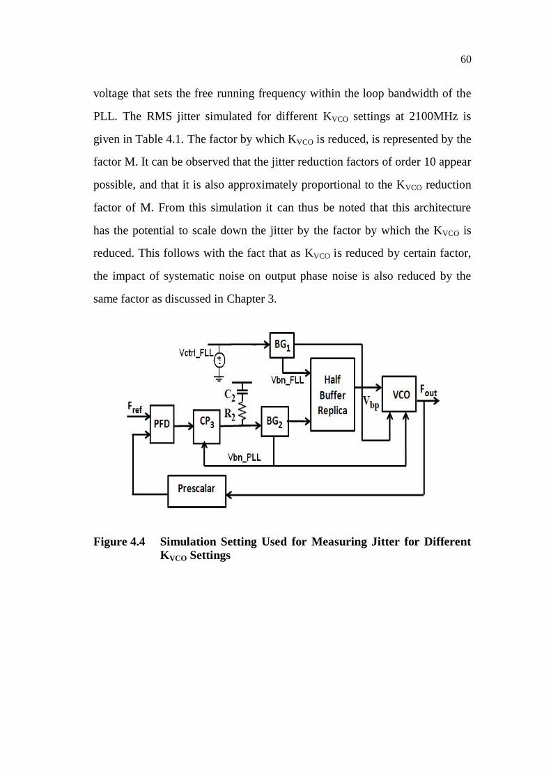
60
voltage that sets the free running frequency within the loop bandwidth of the
PLL. The RMS jitter simulated for different KVCO settings at 2100MHz is
given in Table 4.1. The factor by which KVCO is reduced, is represented by the
factor M. It can be observed that the jitter reduction factors of order 10 appear
possible, and that it is also approximately proportional to the KVCO reduction
factor of M. From this simulation it can thus be noted that this architecture
has the potential to scale down the jitter by the factor by which the KVCO is
reduced. This follows with the fact that as KVCO is reduced by certain factor,
the impact of systematic noise on output phase noise is also reduced by the
same factor as discussed in Chapter 3.
Figure 4.4 Simulation Setting Used for Measuring Jitter for Different KVCO Settings

61
Table 4.1 Jitter Reduction as a Function of KVCO Reduction (Measured at a Frequency of 2100 MHz)
KVCO(MHz/V) RMS Jitter (ps)
KVCO
Reduction factor M
Jitter reduction (compared with
KVCO = 3600MHz/V case)
3600 2.27 1 1
1450 1.04 2.5 2.2
1000 0.94 3.6 2.4
630 0.49 5.7 4.6
540 0.43 6.6 5.3
467 0.30 7.7 7.6
340 0.22 10.5 10.3
From the above tabulation, a KVCO value of 467MHz/V was
chosen for the design of the self biased PLL in the dual loop scheme and the
other parameters namely charge pump current, loop filter capacitance were
used with values as defined in the traditional single loop self biased PLL.
With the choice of KVCO used which is 1/7th (M=7) of the single loop
traditional self biased PLL, the self biased PLL in the dual loop operates with
narrow loop bandwidth with the bandwidth (defined by n) reduced by the
factor of square root of 7, whereas the damping factor was retained to be 1 by
appropriately scaling the loop filter resistance. Circuit simulations were
carried out on the dual loop PLL thus designed. The simulation results
obtained are presented below.

62
4.3 CIRCUIT SIMULATIONS OF DUAL LOOP PLL
The simulation results present the modified VCO gain
characteristic. Using the gain in the characteristic presented, the dual loop
system was designed and the locking characteristic of the designed dual loop
PLL is presented for a nominal frequency of 2.1GHz. Jitter performance of
the dual loop in comparison with tradition single loop PLL is presented by
means of an eye diagram plot. Wide capture range of the dual loop PLL is
presented with capture transients at the extreme operating frequencies,
simulated at worst case process corners. Finally the performance is compared
with the traditional self biased PLL as well as the dual loop PLL implemented
by Song Ying et al (2008) and Akihide Sai
et al (2012).
The gain characteristics of the split tuned VCO is shown in Figure
4.5 and shows a wide linear range of FLL with a gain of 3.6GHz/V, and when
biased at a specific control voltage in its linear range of FLL, the PLL
operates with a low gain of 467MHz/V.
Figure 4.5 VCO Gain Characteristic of Split Tuned VCO

63
The capture transients of the dual loop PLL at the nominal
frequency of 2100MHz is shown in Figure 4.6 by plotting the transient
response of control voltage Vctrl and the bias voltages generated by BG1 and
BG2. The capture transients show the independent tracking nature of the FLL
and PLL incorporated in the dual loop system. The designed FLL is observed
to settle in about 500ns. The PLL is enabled as the frequency difference is
reduced very close to the output frequency (within 2%) and is seen to settle at
about 740ns.
Figure 4.6 Capture Transients of Dual Loop PLL at 2100MHz Output Frequency
Next, in order to compare the jitter performances of the dual and
traditional self biased PLLs, the eye diagram for both cases are plotted in
Figure 4.7 for a nominal output frequency of 2.1GHz. The RMS jitter
computed from this plot was found to be 13ps and 4.3ps respectively for the
traditional and dual loop self biased PLLs, and this corresponds to an
improvement of 67% for the latter.
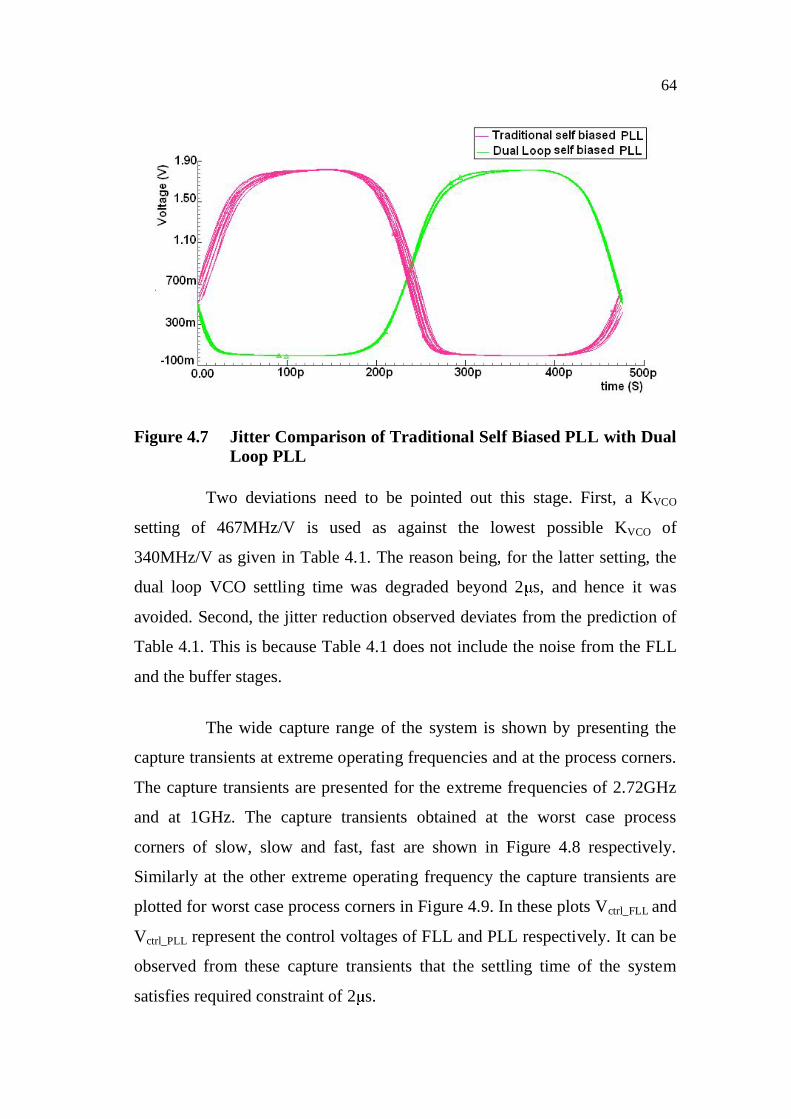
64
Figure 4.7 Jitter Comparison of Traditional Self Biased PLL with Dual Loop PLL
Two deviations need to be pointed out this stage. First, a KVCO
setting of 467MHz/V is used as against the lowest possible KVCO of
340MHz/V as given in Table 4.1. The reason being, for the latter setting, the
dual loop VCO settling time was degraded beyond 2 s, and hence it was
avoided. Second, the jitter reduction observed deviates from the prediction of
Table 4.1. This is because Table 4.1 does not include the noise from the FLL
and the buffer stages.
The wide capture range of the system is shown by presenting the
capture transients at extreme operating frequencies and at the process corners.
The capture transients are presented for the extreme frequencies of 2.72GHz
and at 1GHz. The capture transients obtained at the worst case process
corners of slow, slow and fast, fast are shown in Figure 4.8 respectively.
Similarly at the other extreme operating frequency the capture transients are
plotted for worst case process corners in Figure 4.9. In these plots Vctrl_FLL and
Vctrl_PLL represent the control voltages of FLL and PLL respectively. It can be
observed from these capture transients that the settling time of the system
satisfies required constraint of 2 s.
This image cannot currently be displayed.

65
Figure 4.8 Process Corner Simulation at 1GHz Output
Figure 4.9 Process Corner Simulation at 2.5 GHz Output
The modified dual loop PLL exhibits supply noise rejection characteristic
similar to that of the traditional self biased PLL (characteristic shown in
Figure 2.14). The comparison of the dualloop PLL static supply sensitivity
with the traditional selfbiased PLL is shown in Figure 4.10. From the figure it
can be seen that both the system shows similar rejection characteristic with
the static supply noise sensititvity of the modified dualloop PLL measures to
be 190MHz/V.

66
Figure 4.10 Comparison of static supply rejection characteristic
The dynamic supply rejection characteristic is studied similar to the
traditional self biased PLL by using a sinusoidal supply source of 10MHz
frequency, 10mV peak to peak amplitude and with a DC voltage of 1.8V. The
supply rejection characteristic of the bias voltages is shown in Figure. The
Vbn_coarse and Vbn_fine is observed to remain static whereas Vbp is observed to
track supply variation, thus possessing the dynamic supply rejection
characteristic. In this simulation setup, the output clock shows peak to peak
jitter measure of 12.4ps showing 64% improvement in comparison with the
jitter measured in traditional self biased PLL with noisy power supply. This
improvement closely approximates the improvement obtained with the
noiseless case and thus shows similar rejection characteristic as that of
traditional self biased PLL.

67
Figure 4.11 Bias voltages satisfying the requirement of dynamic supply noise rejection
The performance of the present work is provided in Table 4.2 at the
extreme operating frequency of 2500MHz and a comparison is also provided
with those of the dual loop schemes reported recently in Song Ying J. et al
(2008) and Akihide Sai et al (2012). In terms of jitter and Figure of Merit
(FoM) as expressed in ( (as defined in Akihide Sai et al (2012)), it can be seen
that dual loop self biased PLL outperforms the traditional self biased PLL and
is comparable to the dual loop schemes of Song Ying J. et al (2008), Akihide
Sai et al (2012). The FoM is calculated by using the following expressions.
FoM=10.log(( t/1s)2.(P/1mW)) (4.4)
Here t is the RMS jitter and P represents the peak power measured in locked
condition.
The acquisition time of the dual loop self biased PLL is found to be
inferior compared to the traditional self biased PLL, but still far comparable

68
Table 4.2 Performance Comparison at Extreme Operating Frequency
This Work Result reported in
Akihide Sai et al (2012)
Result reported in
Song Ying J. et al (2008)
Traditional self biased
PLL
Dual loop self biased
PLL
OutputFrequency
(MHz)2720 2500 3100 2100
Reference
(MHz)170 170 108 65.6
Tuning Range
(GHz)0.8-2.7 1-2.5 1.4-3.2 0.86-2.1
KVCO
(MHz/V)3600 470 10 ---
Lock Time s)
Frequencystep (MHz)
0.16
1400
0.470
160
85
940
<3
1300
RMS
Jitter (ps)
(%UI)
1.6
(0.43)
0.45
(0.11)
1.01
(0.31)
1.37
(0.28)
Power (mW) 35.0 37.0 27.5 5.3
FoM(dB)
(as in [7]) -220.7 -231 -225.5 -230
Supply Voltage (V)
1.8 1.8 1.2 1.8
Technology
(nm CMOS) 180 180 65 180

69
to that reported in Song Ying et al (2008) and Akihide Sai et al (2012).
Although this may not be a fair comparison since the present work is based on
simulations only, the main objective here is to identify the key contributing
factors and get estimates of the orders of improvements possible. Also, the
work reported in Akihide Sai et al (2012) lacks supply noise immunity,
process immunity and bandwidth adaptivity features that are inbuilt for the
self biased PLLs.
4.2 SUMMARY
This present chapter presents a systematic procedure for designing
a low jitter self biased PLL based on simulation results. The jitter
improvement factor obtained by using a reduced KVCO was determined
experimentally through simulation. The observation from this simulation
exercise is that in the self biased PLL designed with KVCO scaled, the PLL
bandwidth becomes narrower hence VCO phase noise contribution to the
overall phase noise has to increase and the jitter improvement obtained can be
mitigated. Even under this narrow bandwidth condition, a significant jitter
performance is observed. Hence it can be concluded that the dominant noise
contributor is the charge pump systematic noise and is observed to get scaled
down by the same factor by which the KVCO is reduced. The dual loop
technique thus implemented with reduced KVCO shows significant jitter
reduction. In terms of jitter, lock time and FOM it was shown that the
systematically designed dual loop system performance is either better or
comparable to the recently reported work on a ring oscillator based dual loop
PLL proposed by Akihide Sai et al (2012).