Embed Size (px)
Citation preview

108
CHAPTER 4
FABRICATION AND TESTING
4.1 INTRODUCTION
Based on the design guidelines arrived at in the second and third
chapters the TOF has been realized in SOI wafers using DRIE. The SEM of
the TOF is shown in the Figure 4.1.
Figure 4.1 SEM showing the tilted top view (left) and top view of the
full device (right)
This chapter deals with the microfabrication of the TOF in SOI
wafer and its electromechanical and optical characterizations. Several fixed
PC filters with fixed period, but varying defect widths have been fabricated in
<110> oriented silicon wafers using relatively simpler wet anisotropic

109
etching. These filters are fabricated along with fiber grooves for the easy
alignment of lensed optical fibers for light coupling. The SEM of the top view
of the fixed PC filter fabricated by wet anisotropic etching of <110> oriented
silicon is shown in the Figure 4.2. These fixed filters are used for the
experimental validation of the theoretical predictions of optical
characteristics, minimum insertion loss that can be achieved and also the
thermally induced spectral shift in the transfer function. Therefore this chapter
begins with the fabrication and optical characterization of these fixed filters.
(a) (b)
Figure4.2 (a) Virtual prototype of the fixed PC filter and (b) SEM (top
view) of the fabricated fixed filter
Various fabrication issues related to the high aspect ratio dry and
wet etchings are discussed in this chapter. A novel method for the transfer of
lithographically generated patterns with better CD uniformity and sidewall
verticality on to the etch mask is also described in this chapter.
4.2 FABRICATION OF FIXED PC FILTERS
Fixed PC filters are fabricated in (110) planar silicon wafer by
anisotropic wet etching. The PC layers are defined by etching vertical slits in
to the silicon wafer to form alternating Si/air layers. The silicon wafer
specifications are given in the Table 4.1.

110
Table 4.1 Wafer specifications
Type Orientation Doping concentration Size Thickness Quality
p-type <110> 1013
cm-3
3” 300µm DSP
DSP – Double side polished
In addition to this grating structure, V-grooves are also fabricated to
facilitate on chip fiber alignment for wave propagation normal to the device.
The wet anisotropic etching is carried out using 44% wt. aqueous solution of
KOH. A thermally grown SiO2 layer is used as hard mask during KOH
etching. Several etching trials have been carried out with different
concentrations and temperatures to optimize this recipe, which gives maximum
etch rate with better anisotropy and etch selectivity between silicon and SiO2 etch
mask. The fabrication is a single layer process by which both the PC layers and the
fiber grooves are fabricated simultaneously and is detailed in Figure. 4.3.
Figure 4.3 Single-layer process flow optimized for the fabrication of
PBG structures with fiber grooves.
111
In this process direct laser lithography is used for the pattern
generation and transfer on to the photoresist (AZ5214E). Then this pattern is
transferred on to the SiO2 etch mask by wet etching using buffered
hydrofluoric acid (BHF). Table 4.2 gives the different etch parameters
optimized for the fabrication.
4.2.1 Fabrication issues
Several issues have to be addressed for the optimization of the etch
parameters like etch time, etch mask thickness and strip and gap widths in the
design file before going for the final fabrication. Some of the important fabrication
issues related to wet etching of silicon and SiO2 are described below.
Table 4.2 Different etch parameters optimized using dummy samples
Material Etchant Etch rate (µm/min.) Etch selectivity
(110) 1.6Si
(111)KOH
0.01696.3
SiO2 BHF 0.3 123
4.2.1.1 Wet etching of SiO2 in BHF
The SiO2 etching in BHF is isotropic i.e. the vertical and lateral
etch rate are same and hence it produce large undercut of the same dimension
as that of the etch depth as shown in the Figure 4.4
Figure4.4 Lateral etching of SiO2 in BHF produce large undercut
undesirable for MEMS devices

112
This broadening of the opening due to the lateral etching of SiO2
etch mask should be taken in to account while making the design file i.e. the
strip width in the design file should be adjusted to compensate for this
widening. We used fiber collimators of spot size 25µm to reduce the angular
spectrum entering in to the device. This necessitates PC layers with high
aspect ratio. Besides this fiber grooves must be deep enough to collimate the
light on to the device. The typical fiber diameter is 125µm and taking account
of the spot size of 25µm, the fiber grooves must have 80µm depth. Since this
is a single layer process and taking account of the SiO2 etch rate of 13nm/min.
in the 44% wt. aqueous solution of KOH (increasing temperature leads to
increased oxide etch rate); the oxide thickness should be more than 650nm to
etch 80µm depth in to the silicon substrate. The final dimensions arrived at for
the fabrication is listed in the Table.4.3.
4.2.1.2 Anisotropic etching of different crystal planes in silicon
Wet etching of single crystal silicon using KOH is anisotropic i.e.
different crystal planes etch at different etch rates as discussed in the previous
chapter. This property of (110) silicon is exploited in this work for the
fabrication of PC structures with smooth vertical sidewalls. KOH etching of
(110) silicon exposes three pairs of (111) planes out of which two pairs form
the vertical sidewalls of a parallelogram and the remaining one pair is
projected out 35.260 from the wafer flat as shown in the Figure 4.5.
Figure 4.5 Wet etching of (110) silicon in KOH exposes 3 pairs of (111)
planes

113
The two slanted (111) planes grows as etch depth increases and it
stops etching further once the two planes make contact each other. Therefore
the etch depth is limited by these slanted planes and this depth depends on the
length of the opening in the etch mask through the equation (3.18). Therefore
PC layers must be long enough to give sufficient depth after etching, to
accommodate the large spot size of the incoming light. The final dimensions
of the device set in the design file are listed in the Table 4.4.
4.2.1.3 Mask alignment
In a (110) wafer (110) plane will etch faster than the (111) plane
leaving the former exposed as vertical sidewalls (anisotropy of more than
300). Therefore, in order to etch features with smooth vertical sidewalls, they
must be aligned parallel to the (111) plane during pattern transfer. Optical
flatness and sidewall verticality are the crucial factors which determine the
optical performance of the PC based optical channel drop filter. Therefore the
length of the PC layers must be aligned exactly parallel to the (111) plane
which forms the sidewall during lithography as shown in the Figure 4.6. The fiber
grooves are running perpendicular to the PC layers so that they are not aligned
with the (111) plane and hence is etched with irregular and rough sidewalls.
(a) (b)
Figure 4.6 (a) Parallelogram shaped samples with (111) sidewalls can
be cleaved in (110) wafer and (b) features aligned with the
(111) plane during pattern transfer

114
The etch parameters are set based on the various optical
requirements such as high aspect ratio PC layers needed for accommodating
light beams of 25µm spot size and deep trenches for mounting optical fibers
of diameter 125µm. The design specifications and the required etch
parameters to achieve these specifications are listed in the Table 4.3.
Table 4.3 Device specifications and etch parameters
Device specification Etch parameters
Etch depth (µm)
PC layers Fiber groovesEtching time (s) SiO2 hard mask thickness (µm)
>30 80 50 1
The SiO2 etch mask has a thickness of 1µm and in BHF etching (which opens
the etch window for silicon bulk etching using KOH) the opening will
broaden by 1µm from both sides expanding the window size by 2µm. The
measured etch rate of silicon (111) plane and SiO2 is 16nm/min. and
13nm/min respectively in KOH solution. Therefore during the bulk etching,
the silicon layer (which forms the PC) will further thin down. This finally
requires a thicker width to be set in the mask for regions (gap widths in table
4.4) corresponding to silicon layers. Taking all these into account, the PC
layer dimensions are set to 10µm period with 50% filling fraction which still
gives PBG in the C and L bands. Therefore mask design needs to be
optimized as it has to (i) adjust the length of PC layers to ensure clear vertical
etch depth of more than 30 m (ii) compensate for the undercutting of SiO2
layer during isotropic BHF etching (iii) compensate for the lateral etching of
SiO2 in 44% wt. aqueous solution of KOH at 850C and (iii) compensate for
the lateral etching of Si PC layers in KOH. The mask parameters set for the
fabrication and is listed in the Table 4.4.

115
Table 4.4 Design parameters
Strip width in the design file 3µm
Gap width in the design file 7µm
Length of the PC layers 200µm
Width of the fiber grooves 100µm
Length of the fiber grooves 5mm
The strips and gaps in the design file form the air and silicon layers
for the PC structure respectively. Strip width cannot be reduced further,
because the minimum resolution of the lithography equipment used for this
work is 3µm and hence the final silicon layer thickness will be even lesser
than the expected value of 5µm. The SEM of the fabricated fixed PC filters is
shown in the Figure 4.7.
Figure 4.7 SEM of the fabricated PC filters with fiber grooves
The cross-section image (left) exposes the slanted (111) plane. The depth of
the PC layers and fiber grooves obtained after the fabrication is listed in the
116
Table 4.5. The final PC layer and defect layer thicknesses obtained after all
processes are listed in the Table 4.6.
Table 4.5 Etch depth after fabrication
Etch depth (µm)
PC layers 57.7
Fiber grooves 80
4.3 OPTICAL TESTING OF THE FIXED PC FILTERS
Several fixed filters with varying central defect widths have been
fabricated and the optical results of the best four devices are discussed in this
section. Apart from the irregularities during lithography, the lateral etching of
both the SiO2 and Si layers in the KOH solution is dependent on the gap on
either side of each layer and is hence different for the Si layers defining the
defect region when compared to that for the central Si layer in each PC. This
difference, at the end of 50minutes, will increase with larger defect
dimensions and this was not taken care of in the mask design. Therefore, all
effects put together, the silicon is thinned down non-uniformly leaving the
system highly asymmetric. As discussed in the previous section, the system
can then be treated as asymmetric FP cavity in which the cavity is formed by
two asymmetric or geometrically chirped 1d PC structures say PC1 to the left
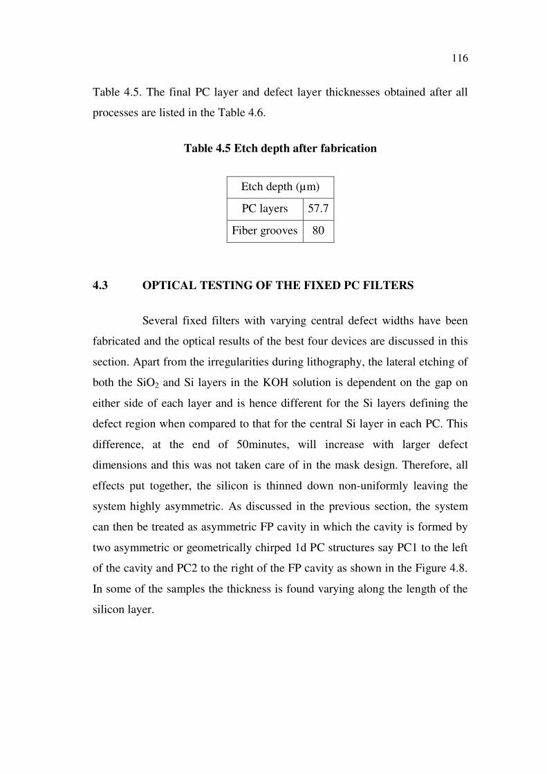
of the cavity and PC2 to the right of the FP cavity as shown in the Figure 4.8.
In some of the samples the thickness is found varying along the length of the
silicon layer.
117
Figure4.8 SEM of fabricated fixed filter shows the PC layer thickness
variation across the PC layers and along the length of the Si
layers
This is attributed to the slight misalignment between the critical
features (PC layers) and the silicon (111) plane during lithography. The
thickness of the PC layers and the percentage variation of lattice constant
from 10µm and filling fraction between the two constituting PC halves of the
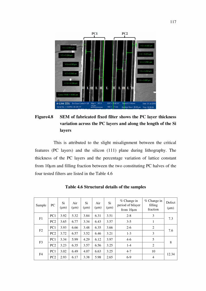
four tested filters are listed in the Table 4.6
Table 4.6 Structural details of the samples
Sample PCSi
m)
Air
m)
Si
m)
Air
m)
Si
m)
% Change in
period of bilayer
from 10 m
% Change in
filling
fraction
Defect
( m)
PC1 3.92 5.32 3.84 6.31 3.51 2-8 3F1
PC2 3.65 6.77 3.34 6.43 3.57 3-5 17.3
PC1 3.93 6.66 3.48 6.35 3.66 2-6 2F2
PC2 3.72 6.57 3.52 6.46 3.21 1-3 37.6
PC1 3.34 5.99 4.29 6.12 3.97 4-6 5F3
PC2 3.23 6.35 3.57 6.56 3.25 1-4 28
PC1 3.02 6.49 4.07 6.63 3.25 4-7 10F4
PC2 2.93 6.17 3.38 5.98 2.65 6-9 412.34

118
H and L in the Figure 4.8 represent the higher (silicon) and lower
(air) refractive index materials respectively.
The optical testing is carried out using a tunable laser of
wavelength range 1506nm-1616nm (Thorlabs INTUN ™TL 1550-B SM)
and an optical spectrum analyzer (OSA) of resolution 0.02nm
(YOKOGAWA AQ6370). The schematic of the optical characterization set
up is shown in the Figure 4.9.
Figure 4.9 Schematic of the optical characterization set up
The SEM images of the four tested filters are depicted in the Figure 4.10.
Figure 4.10 SEM images of the PC filters F1, F2, F3 and F4
119
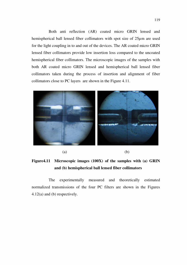
Both anti reflection (AR) coated micro GRIN lensed and
hemispherical ball lensed fiber collimators with spot size of 25µm are used
for the light coupling in to and out of the devices. The AR coated micro GRIN
lensed fiber collimators provide low insertion loss compared to the uncoated
hemispherical fiber collimators. The microscopic images of the samples with
both AR coated micro GRIN lensed and hemispherical ball lensed fiber
collimators taken during the process of insertion and alignment of fiber
collimators close to PC layers are shown in the Figure 4.11.
(a) (b)
Figure4.11 Microscopic images (100X) of the samples with (a) GRIN
and (b) hemispherical ball lensed fiber collimators
The experimentally measured and theoretically estimated
normalized transmissions of the four PC filters are shown in the Figures
4.12(a) and (b) respectively.
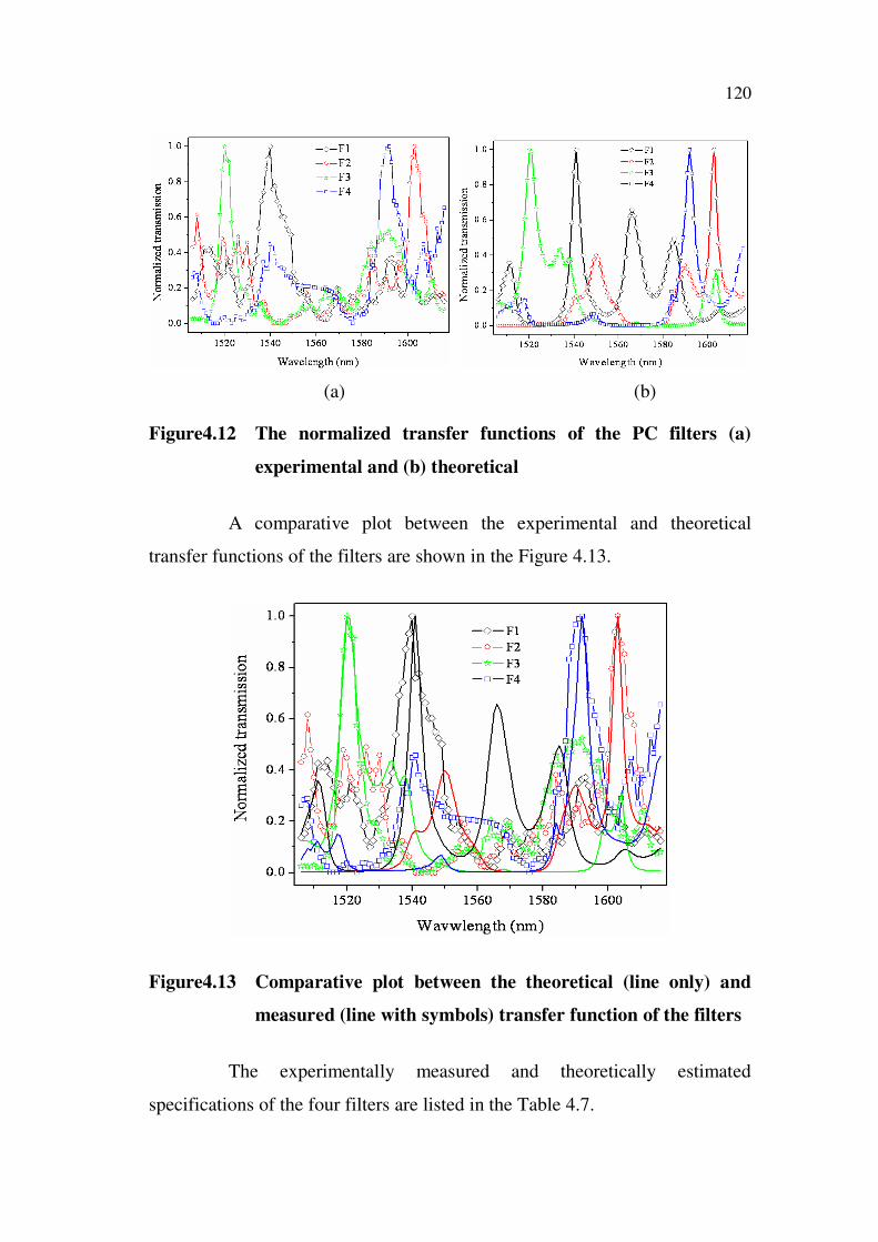
120
(a) (b)
Figure4.12 The normalized transfer functions of the PC filters (a)
experimental and (b) theoretical
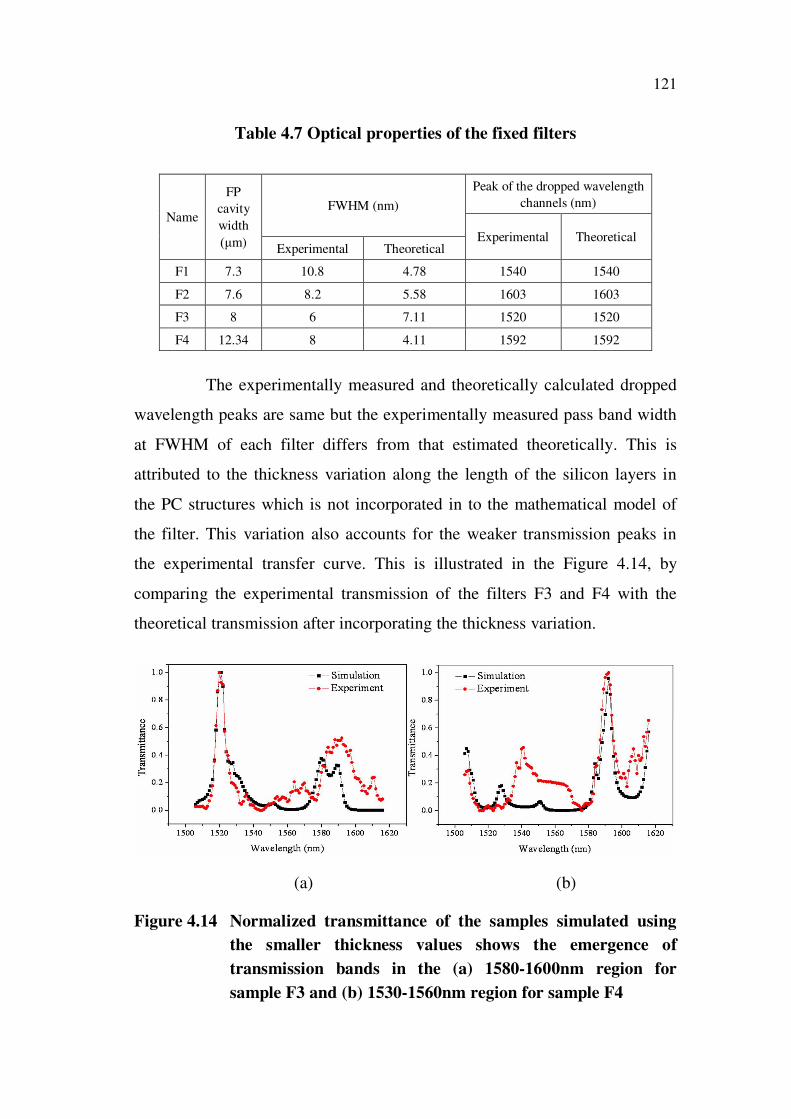
A comparative plot between the experimental and theoretical
transfer functions of the filters are shown in the Figure 4.13.
Figure4.13 Comparative plot between the theoretical (line only) and
measured (line with symbols) transfer function of the filters
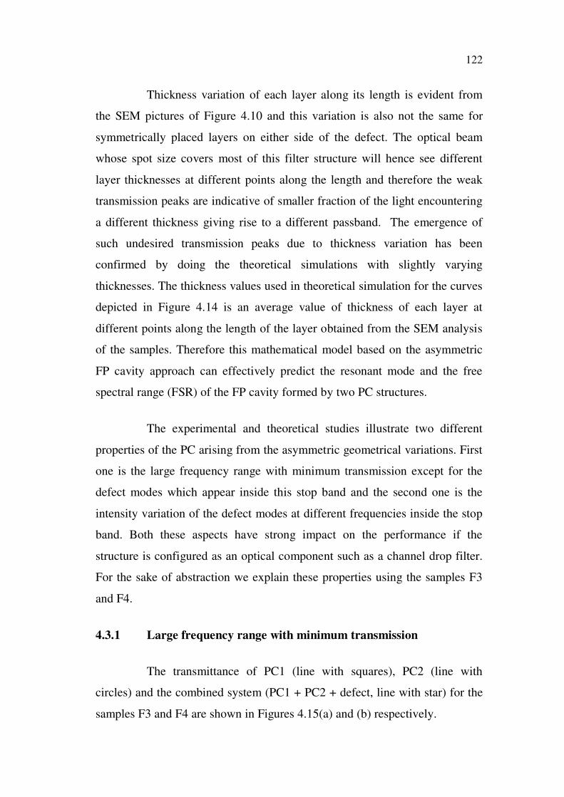
The experimentally measured and theoretically estimated
specifications of the four filters are listed in the Table 4.7.
121
Table 4.7 Optical properties of the fixed filters
Peak of the dropped wavelength
channels (nm)FWHM (nm)Name
FP
cavity
width
m)Experimental Theoretical
Experimental Theoretical
F1 7.3 10.8 4.78 1540 1540
F2 7.6 8.2 5.58 1603 1603
F3 8 6 7.11 1520 1520
F4 12.34 8 4.11 1592 1592
The experimentally measured and theoretically calculated dropped
wavelength peaks are same but the experimentally measured pass band width
at FWHM of each filter differs from that estimated theoretically. This is
attributed to the thickness variation along the length of the silicon layers in
the PC structures which is not incorporated in to the mathematical model of
the filter. This variation also accounts for the weaker transmission peaks in
the experimental transfer curve. This is illustrated in the Figure 4.14, by
comparing the experimental transmission of the filters F3 and F4 with the
theoretical transmission after incorporating the thickness variation.
(a) (b)
Figure 4.14 Normalized transmittance of the samples simulated using
the smaller thickness values shows the emergence of
transmission bands in the (a) 1580-1600nm region for
sample F3 and (b) 1530-1560nm region for sample F4
122
Thickness variation of each layer along its length is evident from
the SEM pictures of Figure 4.10 and this variation is also not the same for
symmetrically placed layers on either side of the defect. The optical beam
whose spot size covers most of this filter structure will hence see different
layer thicknesses at different points along the length and therefore the weak
transmission peaks are indicative of smaller fraction of the light encountering
a different thickness giving rise to a different passband. The emergence of
such undesired transmission peaks due to thickness variation has been
confirmed by doing the theoretical simulations with slightly varying
thicknesses. The thickness values used in theoretical simulation for the curves
depicted in Figure 4.14 is an average value of thickness of each layer at
different points along the length of the layer obtained from the SEM analysis
of the samples. Therefore this mathematical model based on the asymmetric
FP cavity approach can effectively predict the resonant mode and the free
spectral range (FSR) of the FP cavity formed by two PC structures.
The experimental and theoretical studies illustrate two different
properties of the PC arising from the asymmetric geometrical variations. First
one is the large frequency range with minimum transmission except for the
defect modes which appear inside this stop band and the second one is the
intensity variation of the defect modes at different frequencies inside the stop
band. Both these aspects have strong impact on the performance if the
structure is configured as an optical component such as a channel drop filter.
For the sake of abstraction we explain these properties using the samples F3
and F4.
4.3.1 Large frequency range with minimum transmission
The transmittance of PC1 (line with squares), PC2 (line with
circles) and the combined system (PC1 + PC2 + defect, line with star) for the
samples F3 and F4 are shown in Figures 4.15(a) and (b) respectively.

123
(a) (b)
Figure4.15 Spectral response of the two halves PC1 (line with squares)
and PC2 (line with circles) and the total response (line with
solid star) of the combined system for (a) F3 and (b) F4
Since the two halves of the combined system have different lattice
properties (refer to the Table 4.6), they posses distinct spectral characteristics
and in both cases the pass band of PC1 lies inside the stop band of PC2 and
vice versa resulting in a large spectral range with minimum transmission,
except for the defect modes which appear inside this stop band.
Table 4.8 gives the stop and pass bands of PC1, PC2 and the
combined system of PC1, PC2 and the central defect layer for both samples.
In both cases, the transmission peaks of PC1 lie in the stop band of PC2 and
vice versa, effectively lowering the transmission coefficient at the band edges
of the combined system which in turn provides large frequency range of 90
nm with low transmission. In the combined system, only the defect mode has
maximum transmittance approaching 0.9 for those near the band edges (line
with solid star in both Figures 4.15(a) and (b)) and all band edge
transmissions are suppressed. Therefore large FSR can be realized by using
geometrically chirped PCs. Realization of the same FSR using ideal PC’s
would require lower thickness of Si layers i.e. lower filling factors and will
necessitate the use of advanced lithography techniques during the fabrication.

124
Table 4.8 Stop band, band edges and defect modes of the structures
Sample Main Stop bands Band edges Defect mode
PC11514nm-1534nm,
1540nm-1600nm1,2,5 (Fig 4.15(a))
PC21506nm-1560nm
1570nm-1590nm3,4 (Fig 4.15(a))
F3
PC1+PC21506nm-1535nm
1540nm-1595nm
1535nm-1540nm
1595nm-1605nm
(Weak transmission <0.4)
1520nm
PC11510nm-1585nm
1588nm-1616nm1,4 (Fig 4.15(b))
PC21520nm-1547nm
1552nm-1602nm
2,3(Fig 4.15(b))
1602nm-1616nm(weak transmission<0.4)F4
PC1+PC2 1517nm-1616 nm1510nm-1517nm
(weak transmission<0.2)1592nm
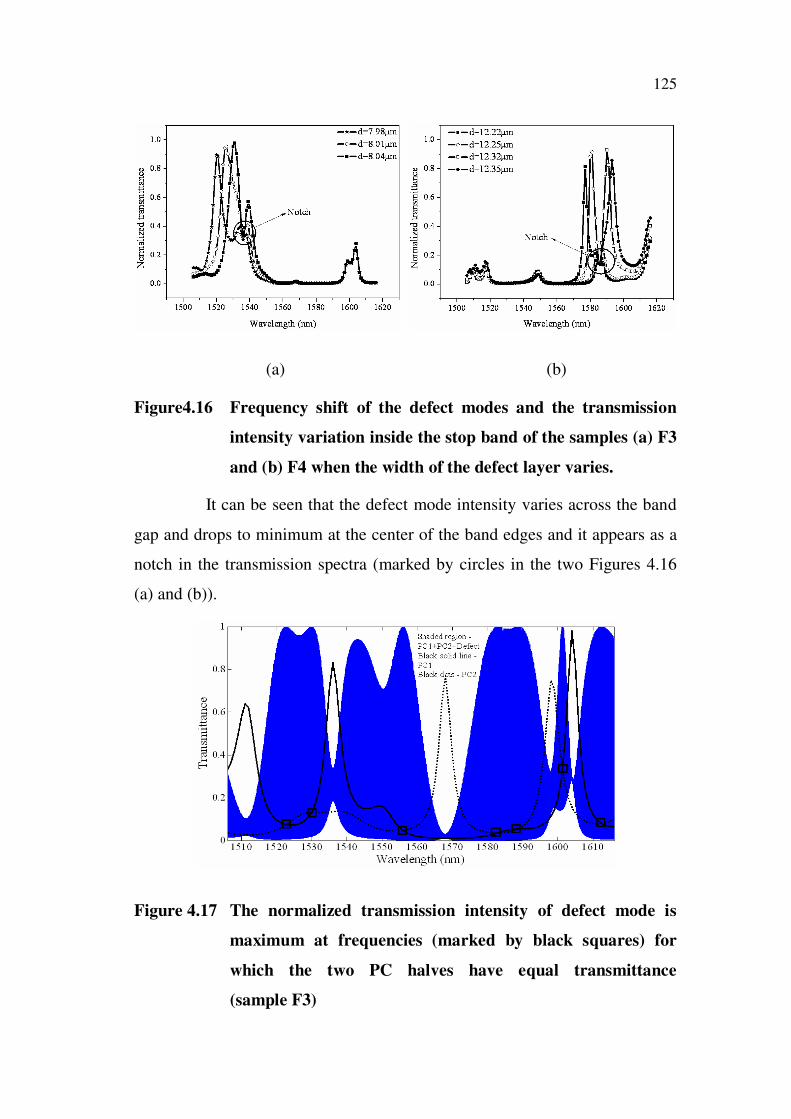
4.3.2 Defect mode intensity variation
In an ideal PC, with central defect layer and geometrically
symmetric structures on either side of the defect layer, the normalized
transmission intensity of the defect mode is unity and is independent of the
defect mode frequency. In the case of samples F3 and F4, which are
geometrically asymmetric with respect to the central defect layer, the intensity
of the defect mode varies with defect mode frequency (refer to Figures 4.16(a)
and (b)). The graphs shown in Figures 4.16(a) and (b) depicting the
theoretical transfer functions of the structures similar to F3 and F4 except for
a change in the width of the central defect layer, confirm that the observed
pass band at 1520 nm for F3 and 1592 nm for F4 are indeed defect modes of
the structures. It is found that the peak of the defect mode shifts towards the
higher wavelength (red shift) as the defect size increases which is as expected
in any Fabry–Perot resonator.
125
(a) (b)
Figure4.16 Frequency shift of the defect modes and the transmission
intensity variation inside the stop band of the samples (a) F3
and (b) F4 when the width of the defect layer varies.
It can be seen that the defect mode intensity varies across the band
gap and drops to minimum at the center of the band edges and it appears as a
notch in the transmission spectra (marked by circles in the two Figures 4.16
(a) and (b)).
Figure 4.17 The normalized transmission intensity of defect mode is
maximum at frequencies (marked by black squares) for
which the two PC halves have equal transmittance
(sample F3)
126
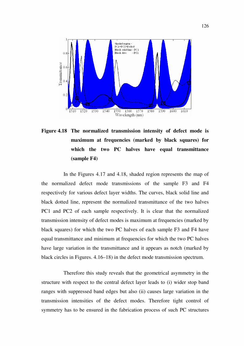
Figure 4.18 The normalized transmission intensity of defect mode is
maximum at frequencies (marked by black squares) for
which the two PC halves have equal transmittance
(sample F4)
In the Figures 4.17 and 4.18, shaded region represents the map of
the normalized defect mode transmissions of the sample F3 and F4
respectively for various defect layer widths. The curves, black solid line and
black dotted line, represent the normalized transmittance of the two halves
PC1 and PC2 of each sample respectively. It is clear that the normalized
transmission intensity of defect modes is maximum at frequencies (marked by
black squares) for which the two PC halves of each sample F3 and F4 have
equal transmittance and minimum at frequencies for which the two PC halves
have large variation in the transmittance and it appears as notch (marked by
black circles in Figures. 4.16–18) in the defect mode transmission spectrum.
Therefore this study reveals that the geometrical asymmetry in the
structure with respect to the central defect layer leads to (i) wider stop band
ranges with suppressed band edges but also (ii) causes large variation in the
transmission intensities of the defect modes. Therefore tight control of
symmetry has to be ensured in the fabrication process of such PC structures
127
for application as low loss channel drop filters in a WDM network. The
intensity variation across the stop band can be predicted by a knowledge of
the transfer profiles of the individual PC’s. Even if a small asymmetry can be
induced in one half of the structure, then the same filter can be reconfigured
to function as a channel drop filter or as a drop and continue filter suitable for
broadcast modes.
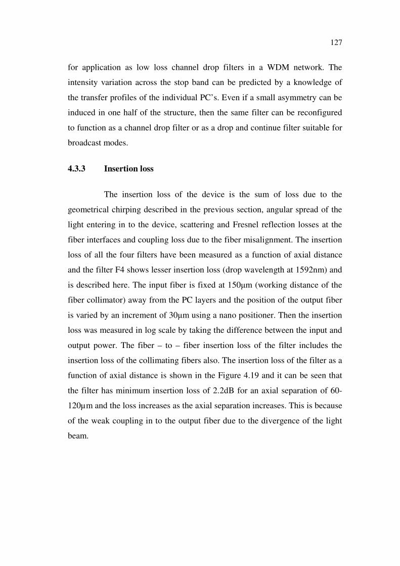
4.3.3 Insertion loss
The insertion loss of the device is the sum of loss due to the
geometrical chirping described in the previous section, angular spread of the
light entering in to the device, scattering and Fresnel reflection losses at the
fiber interfaces and coupling loss due to the fiber misalignment. The insertion
loss of all the four filters have been measured as a function of axial distance
and the filter F4 shows lesser insertion loss (drop wavelength at 1592nm) and
is described here. The input fiber is fixed at 150 m (working distance of the
fiber collimator) away from the PC layers and the position of the output fiber
is varied by an increment of 30 m using a nano positioner. Then the insertion
loss was measured in log scale by taking the difference between the input and
output power. The fiber – to – fiber insertion loss of the filter includes the
insertion loss of the collimating fibers also. The insertion loss of the filter as a
function of axial distance is shown in the Figure 4.19 and it can be seen that
the filter has minimum insertion loss of 2.2dB for an axial separation of 60-
120µm and the loss increases as the axial separation increases. This is because
of the weak coupling in to the output fiber due to the divergence of the light
beam.
128
Figure 4.19 Insertion loss of the filter F4 as a function of axial distance
of the output fiber from the PC layers
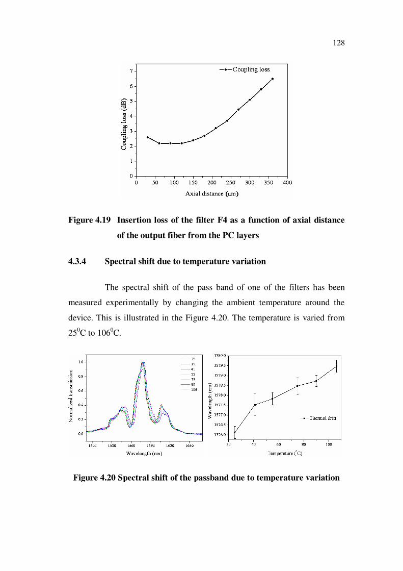
4.3.4 Spectral shift due to temperature variation
The spectral shift of the pass band of one of the filters has been
measured experimentally by changing the ambient temperature around the
device. This is illustrated in the Figure 4.20. The temperature is varied from
250C to 106
0C.
Figure 4.20 Spectral shift of the passband due to temperature variation

129
The set up used for this experiment is shown in the Figure 4.21.
The pass band shift is measured to be 0.04nm/K. This is attributed to the
combined thermo-optic effect and thermal expansion of silicon layers
described in the second chapter.
Figure 4.21 Test set up used for the thermal experiment, inset is the
microscopic image of the device under test (DUT)
The experimentally observed device specifications are listed in the
Table. 4.9.
Table 4.9 Experimental results
Insertion loss 2.2dB
Stopband width >90nm
Passband width <10nm
Thermal drift 0.04nm/K
130
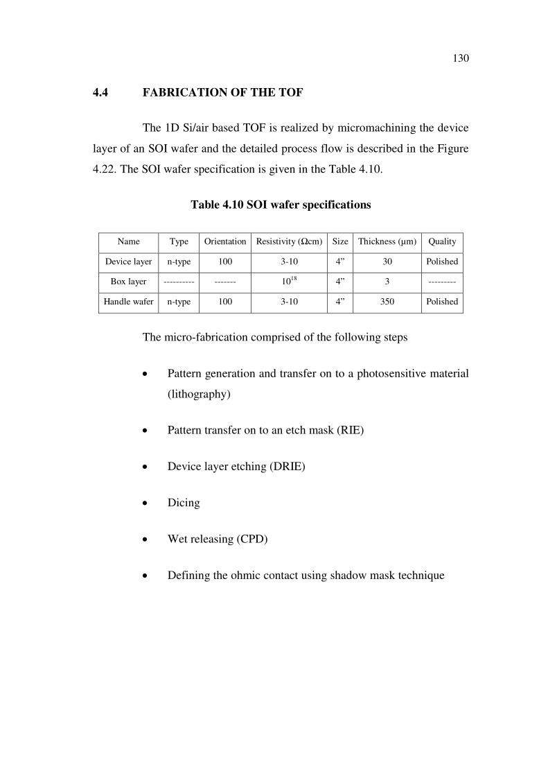
4.4 FABRICATION OF THE TOF
The 1D Si/air based TOF is realized by micromachining the device
layer of an SOI wafer and the detailed process flow is described in the Figure
4.22. The SOI wafer specification is given in the Table 4.10.
Table 4.10 SOI wafer specifications
Name Type Orientation Resistivity ( cm) Size Thickness (µm) Quality
Device layer n-type 100 3-10 4” 30 Polished
Box layer ---------- ------- 1018 4” 3 ---------
Handle wafer n-type 100 3-10 4” 350 Polished
The micro-fabrication comprised of the following steps
Pattern generation and transfer on to a photosensitive material
(lithography)
Pattern transfer on to an etch mask (RIE)
Device layer etching (DRIE)
Dicing
Wet releasing (CPD)
Defining the ohmic contact using shadow mask technique
131
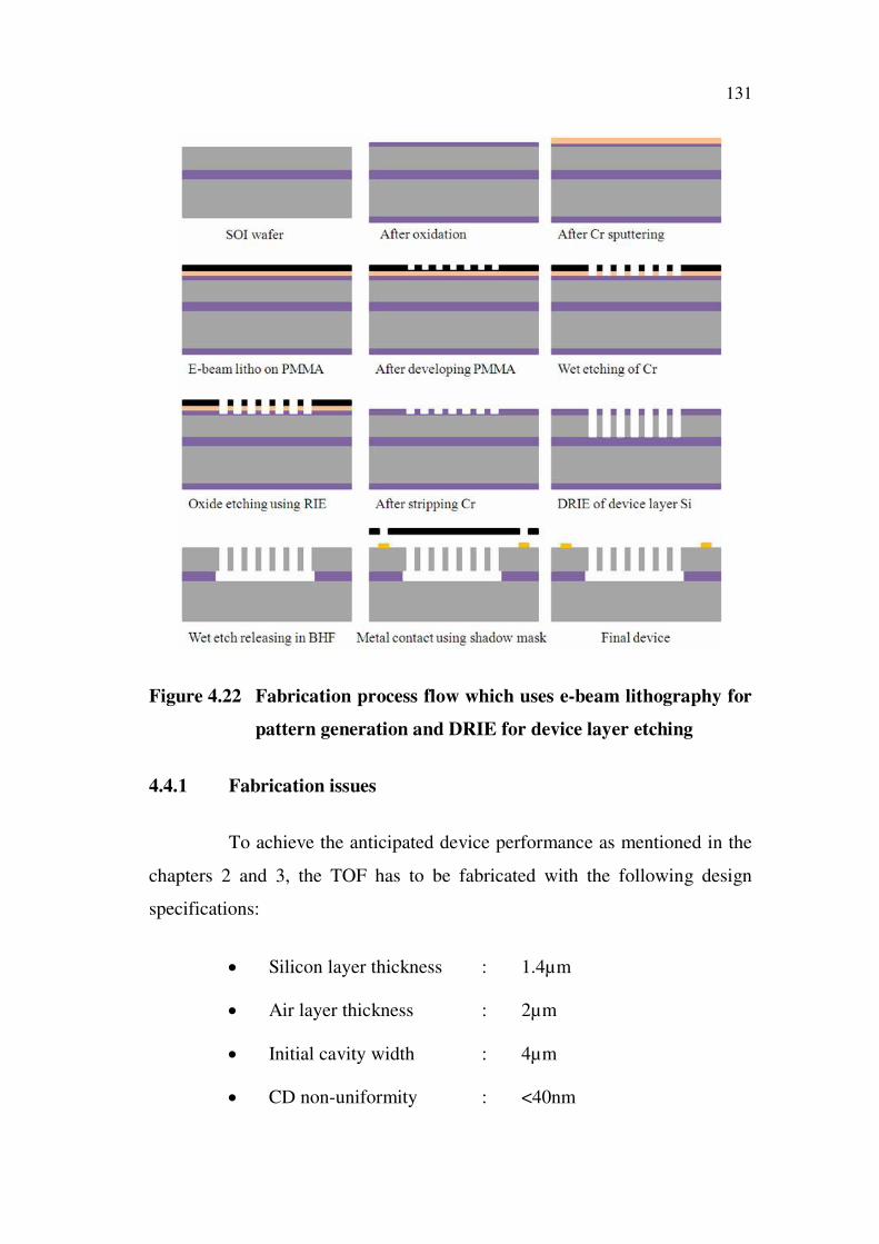
Figure 4.22 Fabrication process flow which uses e-beam lithography for
pattern generation and DRIE for device layer etching
4.4.1 Fabrication issues
To achieve the anticipated device performance as mentioned in the
chapters 2 and 3, the TOF has to be fabricated with the following design
specifications:
Silicon layer thickness : 1.4µm
Air layer thickness : 2µm
Initial cavity width : 4µm
CD non-uniformity : <40nm

132
Roughness (scalloping) : <20nm
Sidewall angle : <0.10
Actuation method : Gap tuning by electrostatic
comb drives
In order to achieve these device specifications, the fabrication is
carried out using e-beam lithography for pattern generation, RIE for pattern
transfer on to the etch hard mask and DRIE for device layer etching. Several
trials have been carried out to optimize the DRIE parameters to meet the
fabrication requirements. The general issues related to DRIE have already
been discussed in the previous chapter. As far as the device is concerned, the
size of the etch window varies between 1µm and 4µm across the sample and
it introduces ARDE. Besides we used small samples of size (2cm×2cm) fixed
on a 4” support wafer using cool grease for DRIE. This leads to the oxide
hard mask erosion due to overheating of the samples during DRIE. By taking
all these issues in to account the following DRIE recipe is optimized for the
fabrication (Table 4.11). We used STS advanced silicon etcher for this
purpose.
Table 4.11 DRIE recipe
SF6 200Gas flow rate (sccm)
C4F8 80
Etching time (second) 1
Passivation time (second) 1
The etch parameters obtained by etching a dummy sample using
this recipe is listed in the Table 4.12.
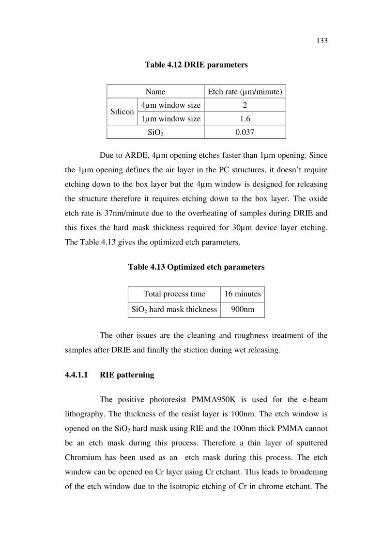
133
Table 4.12 DRIE parameters
Name Etch rate (µm/minute)
4µm window size 2Silicon
1µm window size 1.6
SiO2 0.037
Due to ARDE, 4µm opening etches faster than 1µm opening. Since
the 1µm opening defines the air layer in the PC structures, it doesn’t require
etching down to the box layer but the 4µm window is designed for releasing
the structure therefore it requires etching down to the box layer. The oxide
etch rate is 37nm/minute due to the overheating of samples during DRIE and
this fixes the hard mask thickness required for 30µm device layer etching.
The Table 4.13 gives the optimized etch parameters.
Table 4.13 Optimized etch parameters
Total process time 16 minutes
SiO2 hard mask thickness 900nm
The other issues are the cleaning and roughness treatment of the
samples after DRIE and finally the stiction during wet releasing.
4.4.1.1 RIE patterning
The positive photoresist PMMA950K is used for the e-beam
lithography. The thickness of the resist layer is 100nm. The etch window is
opened on the SiO2 hard mask using RIE and the 100nm thick PMMA cannot
be an etch mask during this process. Therefore a thin layer of sputtered
Chromium has been used as an etch mask during this process. The etch
window can be opened on Cr layer using Cr etchant. This leads to broadening
of the etch window due to the isotropic etching of Cr in chrome etchant. The

134
RIE recipe for SiO2 etching is given in the Table 4.14, which is optimized as
per the design requirements using dummy samples. An ANNELVA made
DEM451 RIE system has been used for this purpose.
Table 4.14 RIE recipe
CF4 50Gas flow rate (sccm)
O2 5
RF power (W) 150
Champer pressure (mTorr) 40
The etch parameters obtained by etching a dummy sample using
this recipe is shown in the Table 4.15.
Table 4.15 RIE parameters
SiO2 etch rate (nm/minute) 45
Cr etch rate (nm/minute) 2.8
Therefore the thickness of the Cr layer and time required to etch
900nm of SiO2 is fixed based on these RIE parameters and are listed in the
Table 4.16.
Table 4.16 Optimized etch parameters
Total process time (minutes) 20
Thickness of the Cr layer (nm) 100
The wet etching of Cr layer using chrome etchant leads to the
broadening of the etch window from both sides by the equal amount of the
thickness of the Cr layer. The window further broadens during the RIE of the
SiO2 hard mask. Therefore in the design file the strip width is set to 800nm,
135
which corresponds to the air layer in the PC mirror and the gap width is set to
2.6µm which corresponds to the silicon layer in the PC mirror. This reverse
engineering is expected to yield the desired silicon and air layer thicknesses.
The other advantage of using thin layer of Cr as etch mask in RIE for pattern
transfer is the improved sidewall verticality and CD uniformity across the wafer.
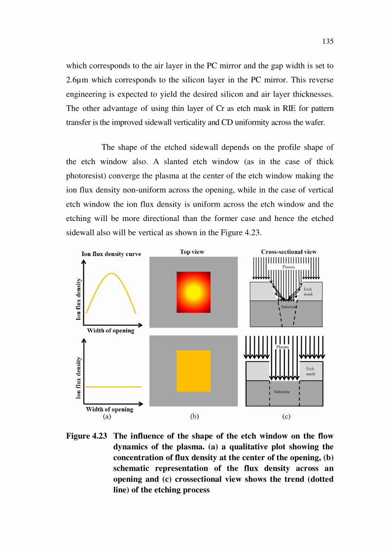
The shape of the etched sidewall depends on the profile shape of
the etch window also. A slanted etch window (as in the case of thick
photoresist) converge the plasma at the center of the etch window making the
ion flux density non-uniform across the opening, while in the case of vertical
etch window the ion flux density is uniform across the etch window and the
etching will be more directional than the former case and hence the etched
sidewall also will be vertical as shown in the Figure 4.23.
Figure 4.23 The influence of the shape of the etch window on the flow
dynamics of the plasma. (a) a qualitative plot showing the
concentration of flux density at the center of the opening, (b)
schematic representation of the flux density across an
opening and (c) crossectional view shows the trend (dotted
line) of the etching process
136
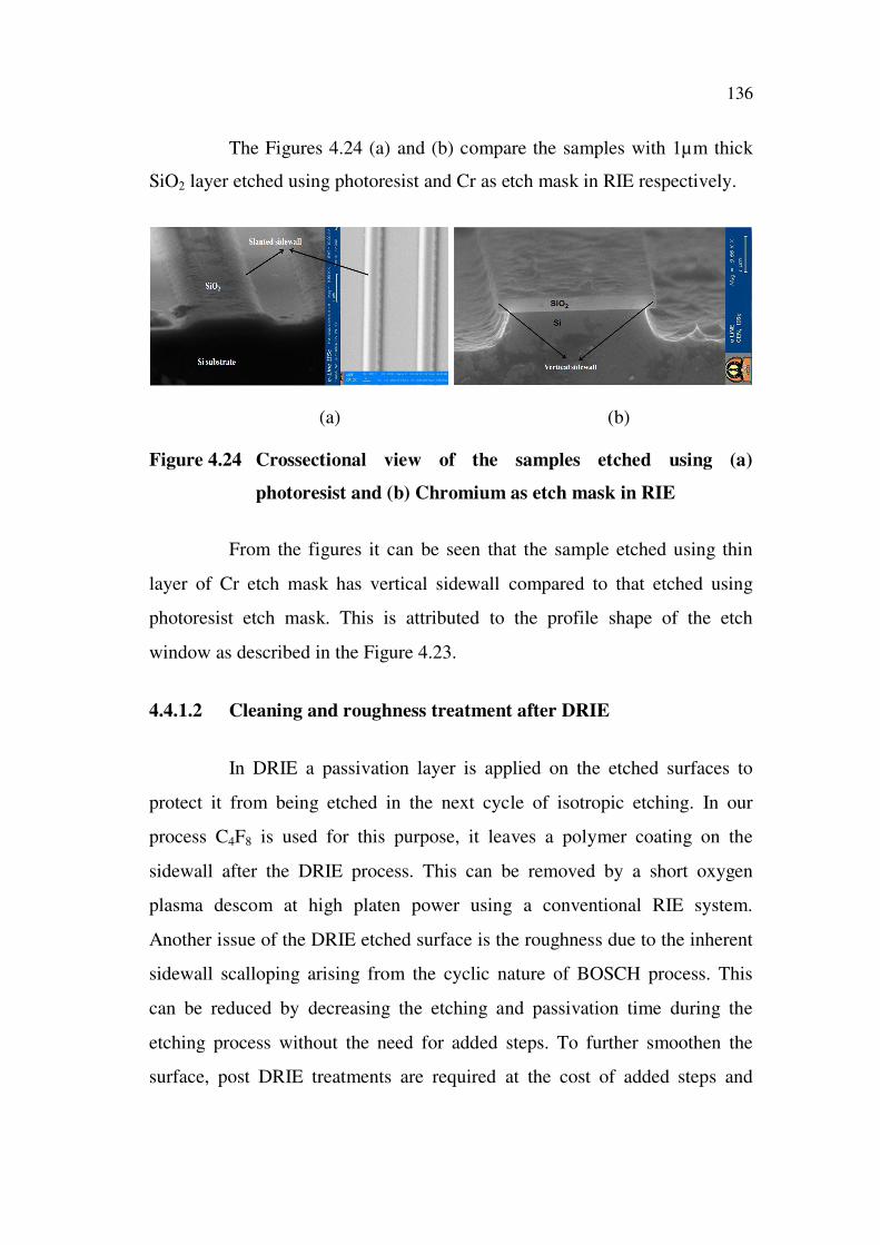
The Figures 4.24 (a) and (b) compare the samples with 1µm thick
SiO2 layer etched using photoresist and Cr as etch mask in RIE respectively.
(a) (b)
Figure 4.24 Crossectional view of the samples etched using (a)
photoresist and (b) Chromium as etch mask in RIE
From the figures it can be seen that the sample etched using thin
layer of Cr etch mask has vertical sidewall compared to that etched using
photoresist etch mask. This is attributed to the profile shape of the etch
window as described in the Figure 4.23.
4.4.1.2 Cleaning and roughness treatment after DRIE
In DRIE a passivation layer is applied on the etched surfaces to
protect it from being etched in the next cycle of isotropic etching. In our
process C4F8 is used for this purpose, it leaves a polymer coating on the
sidewall after the DRIE process. This can be removed by a short oxygen
plasma descom at high platen power using a conventional RIE system.
Another issue of the DRIE etched surface is the roughness due to the inherent
sidewall scalloping arising from the cyclic nature of BOSCH process. This
can be reduced by decreasing the etching and passivation time during the
etching process without the need for added steps. To further smoothen the
surface, post DRIE treatments are required at the cost of added steps and
137
complexity. Usually oxidation and subsequent removal of the oxide is
suggested for the roughness treatment of the DRIE etched samples.
In this work, the same Annelva made DEM451 system was used for
the oxygen plasma descom at 350W for one hour. The roughness is removed
by growing a 100nm thick oxide layer using dry oxidation and subsequently
removing it by wet etching using BHF solution. This is done along with the
releasing process.
4.4.1.3 Stiction during wet releasing
In micromachining using wet processes, closely spaced delicate
membranes or released structures will tend to deflect and stick together due to
the surface tension induced by the trapped liquid droplets attached to the
surfaces during the final rinsing and drying operations.
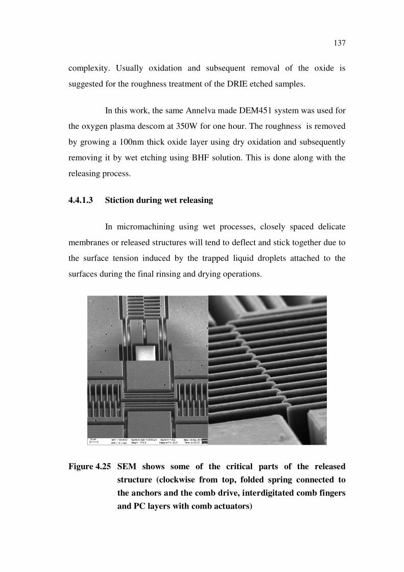
Figure 4.25 SEM shows some of the critical parts of the released
structure (clockwise from top, folded spring connected to
the anchors and the comb drive, interdigitated comb fingers
and PC layers with comb actuators)

138
This phenomenon is known as stiction. This is prominent in MEMS
devices having released structures with large area. This can be minimized by
using dry releasing or critical point drying. In our fabrication process the wet
releasing of the movable PC mirrors is performed using CPD with liquid CO2
at 310C and 1100psi. The SEM of the released TOF is shown in the Figure
4.25and the SEM of the smooth vertical PC layers is shown in the Figure 4.26.
Figure4.26 SEM of the PC layers (tilted top view) shows smooth
sidewalls after dry oxidation followed by BHF dip
The critical device dimensions finally achieved in the fabricated
device is reported in Table 4.17.
Table 4.17 Structural dimensions of the PC layers and FP cavity
Design ( m) Fabricated device ( m)Name
Si Air Cavity Si Air Si Air Si Cavity
PC1 1.4 2 1.65 1.65 1.69 1.87 1.78
PC2 1.4 24
1.74 1.87 1.69 1.65 1.693.9

139
In our device the electrostatic comb drive actuators have a total of
50 comb fingers (25 in each pair) and the initial overlap go between them is
m with an inter finger gap x of 1 m in the overlapping region. The
structural dimension of the actuator part after fabrication is given in the Table
4.18.
Table 4.18 Structural dimensions of the actuator parts
Name PC layers Comb fingers Support springs
Length ( m) 60 23 250
Breadth ( m) 9 1.8 1.8
Thickness ( m) 30 30 30
Gap ( m) 3.9 1 4
The final step of the fabrication is the dicing of the sample,
patterning of metal pads for ohmic contact and simple packaging. The metal
pads of 500µm diameter are defined by shadow mask and RF sputtering. A
Ti/Au layer of thickness 100nm/300nm is sputtered using an Annelva made
RF sputtering system.
Figure 4.27 Photograph of the MEMS chip containing eight TOF’s
Finally the chip of dimension 16mm×8mm containing 7 devices separated
from each other is mounted on a 16 head electronic package and wire bonding
140
between electronic heads and metal pads are done for electric contact. The
photograph of the MEMS chip is shown in the Figure 4.27.
4.5 ELECTROMECHANICAL TESTING OF THE TOF
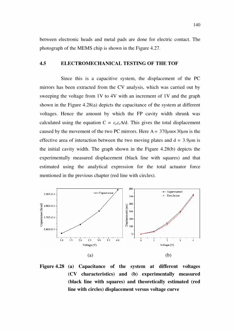
Since this is a capacitive system, the displacement of the PC
mirrors has been extracted from the CV analysis, which was carried out by
sweeping the voltage from 1V to 4V with an increment of 1V and the graph
shown in the Figure 4.28(a) depicts the capacitance of the system at different
voltages. Hence the amount by which the FP cavity width shrunk was
calculated using the equation C = o rA/d. This gives the total displacement
caused by the movement of the two PC mirrors. Here A = 370 m× 30 m is the
effective area of interaction between the two moving plates and d = 3.9 m is
the initial cavity width. The graph shown in the Figure 4.28(b) depicts the
experimentally measured displacement (black line with squares) and that
estimated using the analytical expression for the total actuator force
mentioned in the previous chapter (red line with circles).
(a) (b)
Figure 4.28 (a) Capacitance of the system at different voltages
(CV characteristics) and (b) experimentally measured
(black line with squares) and theoretically estimated (red
line with circles) displacement versus voltage curve

141
The measured and theoretically estimated displacement and cavity
widths are listed in the Table 4.19. The lateral stiffness (k) of the folded
support springs was extracted from the finite element model of the structure
simulated using commercial MEMS CAD tool and it is found to be 0.42N/m.
The geometry of the fabricated structure obtained from SEM analysis (refer to
Tables 4.17 and 4.18) was used for this modeling.
Table 4.19 Results of mechanical analysis
Displacement (nm) Cavity width ( m)Voltage (V) C (fF)
Expt. Theoretical Expt. Theoretical
1 25.66 35.99 31.96 3.864 3.868
2 26.42 146.41 127.88 3.754 3.772
3 27.57 303.04 287.96 3.597 3.61
4 29.38 525.33 509.61 3.375 3.39
The microscopic images of the device taken during actuation are
shown in the Figures 4.29, 4.30 and 4.31.
(a) (b)
Figure 4.29 The PC based FP cavity of the TOF (a) with load and (b)
without load

142
(a) (b)
Figure 4.30 Microscopic images of the comb drives (a) with and (b)
without load
(a) (b)
Figure 4.31 Microscopic images of the support beams during actuation
(a) support beams attached to the anchors and (b) support
beams attached to the comb drives
143
4.6 OPTICAL TESTING OF THE TOF
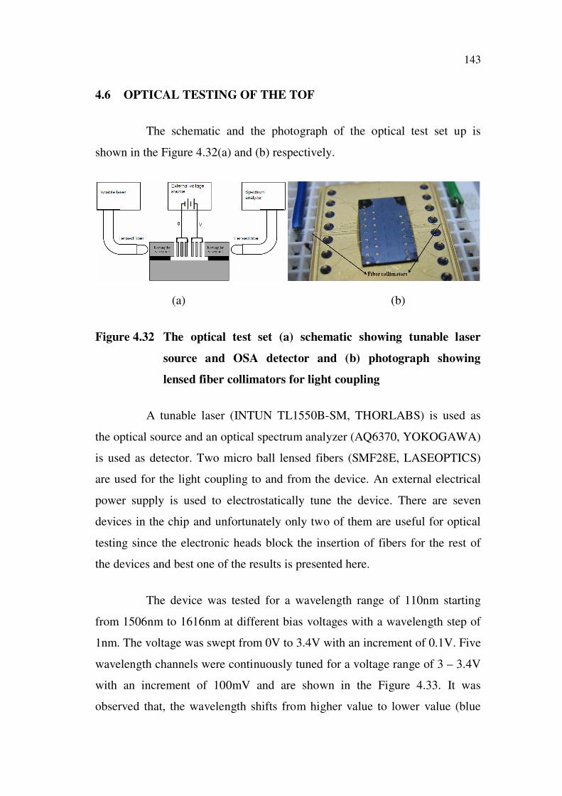
The schematic and the photograph of the optical test set up is
shown in the Figure 4.32(a) and (b) respectively.
(a) (b)
Figure 4.32 The optical test set (a) schematic showing tunable laser
source and OSA detector and (b) photograph showing
lensed fiber collimators for light coupling
A tunable laser (INTUN TL1550B-SM, THORLABS) is used as
the optical source and an optical spectrum analyzer (AQ6370, YOKOGAWA)
is used as detector. Two micro ball lensed fibers (SMF28E, LASEOPTICS)
are used for the light coupling to and from the device. An external electrical
power supply is used to electrostatically tune the device. There are seven
devices in the chip and unfortunately only two of them are useful for optical
testing since the electronic heads block the insertion of fibers for the rest of
the devices and best one of the results is presented here.
The device was tested for a wavelength range of 110nm starting
from 1506nm to 1616nm at different bias voltages with a wavelength step of
1nm. The voltage was swept from 0V to 3.4V with an increment of 0.1V. Five
wavelength channels were continuously tuned for a voltage range of 3 – 3.4V
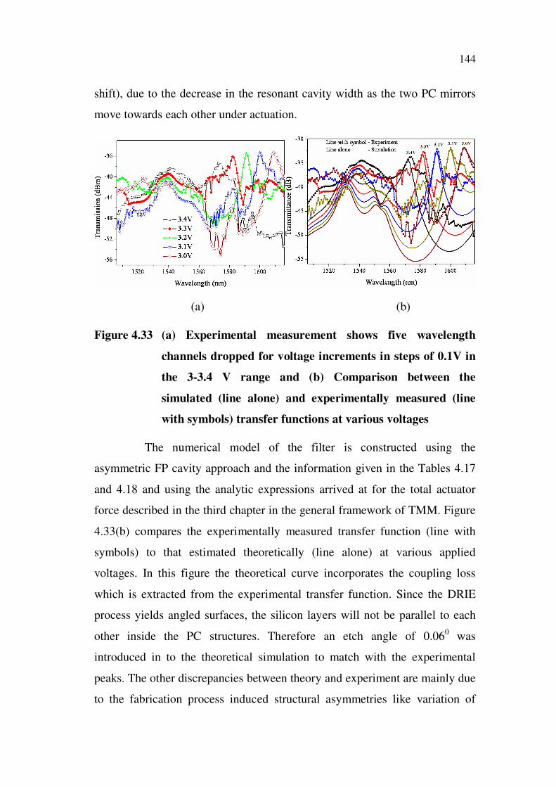
with an increment of 100mV and are shown in the Figure 4.33. It was
observed that, the wavelength shifts from higher value to lower value (blue
144
shift), due to the decrease in the resonant cavity width as the two PC mirrors
move towards each other under actuation.
(a) (b)
Figure 4.33 (a) Experimental measurement shows five wavelength
channels dropped for voltage increments in steps of 0.1V in
the 3-3.4 V range and (b) Comparison between the
simulated (line alone) and experimentally measured (line
with symbols) transfer functions at various voltages
The numerical model of the filter is constructed using the
asymmetric FP cavity approach and the information given in the Tables 4.17
and 4.18 and using the analytic expressions arrived at for the total actuator
force described in the third chapter in the general framework of TMM. Figure
4.33(b) compares the experimentally measured transfer function (line with
symbols) to that estimated theoretically (line alone) at various applied
voltages. In this figure the theoretical curve incorporates the coupling loss
which is extracted from the experimental transfer function. Since the DRIE
process yields angled surfaces, the silicon layers will not be parallel to each
other inside the PC structures. Therefore an etch angle of 0.060 was
introduced in to the theoretical simulation to match with the experimental
peaks. The other discrepancies between theory and experiment are mainly due
to the fabrication process induced structural asymmetries like variation of

145
thickness along the length of the same Si layer, which has not been
incorporated in to the theory. It can also be seen from the figures 4.33(a) and
(b) that the intensity of the dropped channels varies across the band gap. This
is attributed to the geometrical chirping of the PC layers and has already been
discussed in the case of fixed PC filters.
A comparison between the experimental and theoretical
transmittance is given in the Table 4.20. The pass band width for each
dropped channel is less than 8nm.
Table 4.20 Results of optical analysis
Peak wavelength (nm) Pass band width (nm)Voltage (V)
Experiment Simulation Experiment Simulation
3 1609 1609 7.64 8.93
3.1 1600 1600 6.38 4.74
3.2 1591 1591 4.47 3.57
3.3 1582 1581 5.76 3.1
3.4 1574 1572 4.83 2.57
In our design the light is first coupled to the input waveguide of
length 4mm using lensed fiber and then coupled to the device. From the
device the light is coupled to the output waveguide of same length and then to
the lensed fiber. This introduces large coupling loss at the waveguide edges.
This along with the scattering and Fresnel reflection losses in the waveguide
contributed to the high loss (>20dB) reported in the Figure 4.33(b). Therefore
the filter will have to be necessarily fabricated using a two step process with
in-plane fiber grooves to facilitate free space coupling of light in to and out of
the device using AR coated micro GRIN lensed fibers.
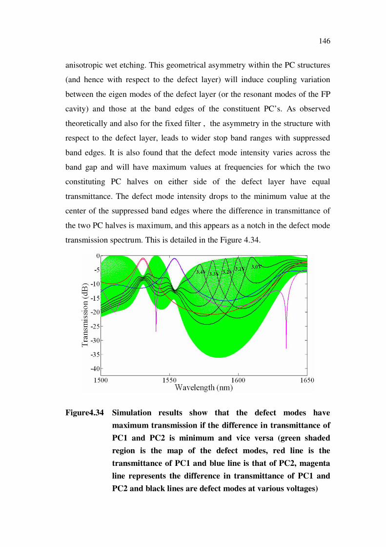
It can be seen from the Table 4.16 that the two PC halves on either
side of the resonant cavity are asymmetric, i.e. PC1 has an average filling
fraction of 0.483 and that of PC2 is 0.501, i.e. a filling fraction change of
1.8% between the two PC mirrors which is lesser than that obtained using
146
anisotropic wet etching. This geometrical asymmetry within the PC structures
(and hence with respect to the defect layer) will induce coupling variation
between the eigen modes of the defect layer (or the resonant modes of the FP
cavity) and those at the band edges of the constituent PC’s. As observed
theoretically and also for the fixed filter , the asymmetry in the structure with
respect to the defect layer, leads to wider stop band ranges with suppressed
band edges. It is also found that the defect mode intensity varies across the
band gap and will have maximum values at frequencies for which the two
constituting PC halves on either side of the defect layer have equal
transmittance. The defect mode intensity drops to the minimum value at the
center of the suppressed band edges where the difference in transmittance of
the two PC halves is maximum, and this appears as a notch in the defect mode
transmission spectrum. This is detailed in the Figure 4.34.
Figure4.34 Simulation results show that the defect modes have
maximum transmission if the difference in transmittance of
PC1 and PC2 is minimum and vice versa (green shaded
region is the map of the defect modes, red line is the
transmittance of PC1 and blue line is that of PC2, magenta
line represents the difference in transmittance of PC1 and
PC2 and black lines are defect modes at various voltages)

147
To conclude, when compared with the similar designs reported
earlier by Lipson et al (2007), Saadany et al (2006) and Pruessner et al (2008),
we have designed and fabricated PC filters with small filling factor of 3.4µm
which ensures large PBG and hence large tuning range. We have
demonstrated more than 70nm tuning range in the C and L band with a high
wavelength tuning sensitivity of 9nm/100mV. The pass band width of our
filter is greater than that reported in the above mentioned references due to the
geometrical chirping of the PC layers. The important device parameters
achieved with this TOF is listed in the Table 4.21.
Table 4.21 Device specifications
Tuning range 70nm (1550nm-1620nm)
Tuning efficiency 0.09nm/mV
Actuation voltage <4V
Reconfiguration time (theoretical prediction) <100µs
Passband width <8nm
Insertion loss >20dB
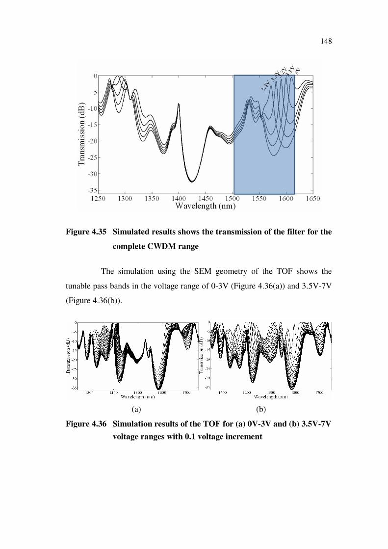
The Figure 4.35 depicts the simulated transfer function of the TOF
for the entire CWDM grid using the geometry extracted from the SEM
analysis (Table 4.17 and 4.18) for an applied voltage range of 3V – 3.4V with
an increment of 0.1V. The shaded region represents the experimentally tested
region of the spectrum.
148
Figure 4.35 Simulated results shows the transmission of the filter for the
complete CWDM range
The simulation using the SEM geometry of the TOF shows the
tunable pass bands in the voltage range of 0-3V (Figure 4.36(a)) and 3.5V-7V
(Figure 4.36(b)).
(a) (b)
Figure 4.36 Simulation results of the TOF for (a) 0V-3V and (b) 3.5V-7V
voltage ranges with 0.1 voltage increment

149
4.7 CONCLUSION
The fabrication and characterization of fixed and tunable PC optical
channel drop filters have been discussed in this chapter. Wet anisotropic etching
of (110) silicon was used for the fabrication of fixed filters with fiber grooves. It
guarantees smooth vertical sidewalls crucial for the low loss performance of the
filter. It can be achieved by manipulating a few etch parameters such as etching
temperature and etchant concentration. While in the case of anisotropic DRIE
using BOSCH process used for the fabrication of TOF, requires the manipulation
of a lot of process parameters to achieve the design specifications and even post
DRIE treatments are required to achieve optical flatness. The minimum insertion
loss achieved with the wet anisotropic etching is 2.2dB. The insertion loss of
more than 20dB reported for the TOF is mainly due to the signal loss in the
waveguide due to Fresnel reflection and scattering due to structural
imperfections. The TOF has wide tuning range of 70nm in the L bands of the
CWDM grid. The tuning sensitivity is 0.09nm/mV which brings down the
requirement of actuation voltage. The pass band width is 8nm, which will be
required in the CWDM networks operated by uncooled semiconductor lasers.
Therefore the wide pass band width can accommodate the peak wavelength shift
of the laser due to temperature variation and ageing and also the thermally
induced spectral shift of the filter itself. The design modification required for the
improvement of the optical as well as electromechanical performance will be
discussed in the next chapter.