Embed Size (px)
Citation preview
Chapter 4MARIE: An
Introduction to a
Simple Computer
2
4.2 CPU Basics
• The computer’s CPU fetches, decodes, and
executes program instructions.
• The two principal parts of the CPU are the datapath
and the control unit.
– The datapath consists of an arithmetic-logic unit and
storage units (registers) that are interconnected by a data
bus that is also connected to main memory.
– Various CPU components perform sequenced operations
according to signals provided by its control unit.
3
• Registers hold data that can be readily accessed by
the CPU.
• They can be implemented using D flip-flops.
– A 32-bit register requires 32 D flip-flops.
• The arithmetic-logic unit (ALU) carries out logical and
arithmetic operations as directed by the control unit.
• The control unit determines which actions to carry out
according to the values in a program counter register
and a status register.
4.2 CPU Basics
4
• Buses consist of data lines, control lines, and
address lines.
• While the data lines convey bits from one device to
another, control lines determine the direction of data
flow, and when each device can access the bus.
• Address lines determine the location of the source
or destination of the data.
The next slide shows a model bus configuration.
4.3 The Bus

5
4.3 The Bus
6
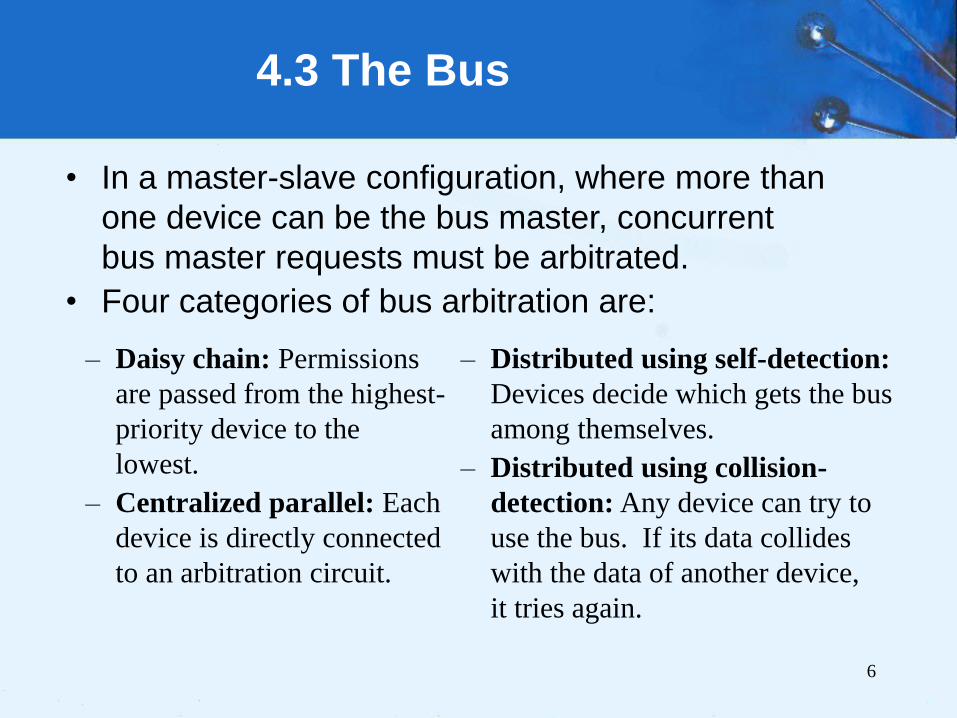
– Distributed using self-detection:
Devices decide which gets the bus
among themselves.
– Distributed using collision-
detection: Any device can try to
use the bus. If its data collides
with the data of another device,
it tries again.
– Daisy chain: Permissions
are passed from the highest-
priority device to the
lowest.
– Centralized parallel: Each
device is directly connected
to an arbitration circuit.
• In a master-slave configuration, where more than
one device can be the bus master, concurrent
bus master requests must be arbitrated.
• Four categories of bus arbitration are:
4.3 The Bus
7
4.4 Clocks
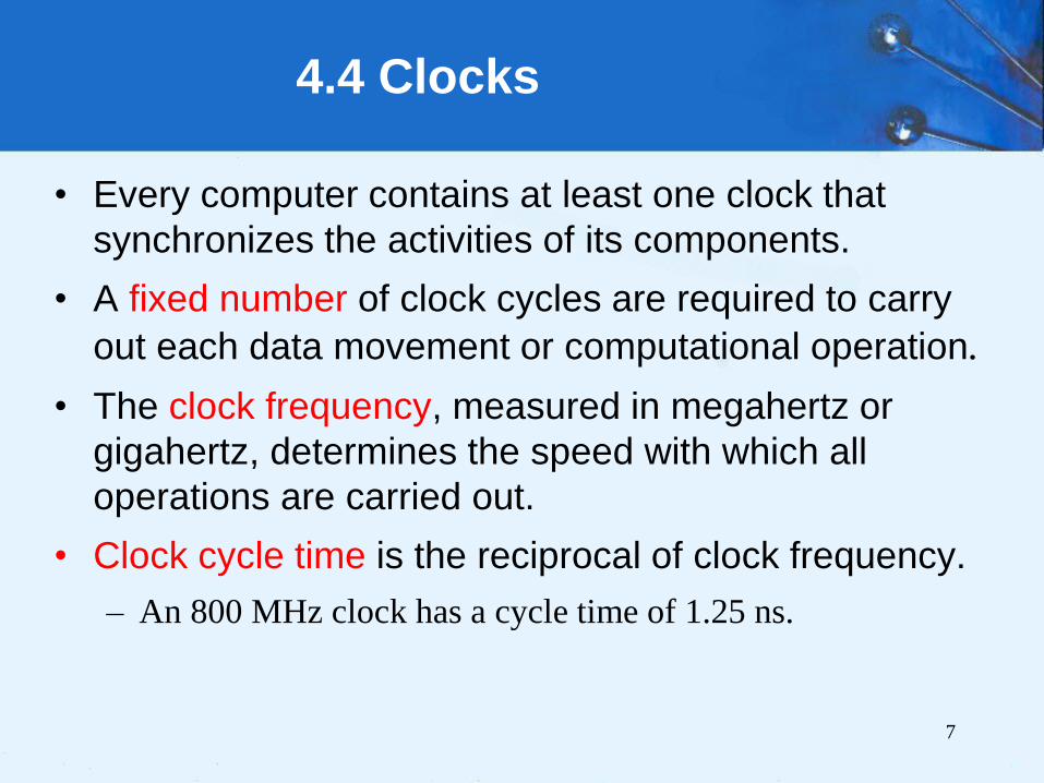
• Every computer contains at least one clock that
synchronizes the activities of its components.
• A fixed number of clock cycles are required to carry
out each data movement or computational operation.
• The clock frequency, measured in megahertz or
gigahertz, determines the speed with which all
operations are carried out.
• Clock cycle time is the reciprocal of clock frequency.
– An 800 MHz clock has a cycle time of 1.25 ns.

8
• Clock speed should not be confused with CPU
performance.
• The CPU time required to run a program is given by
the general performance equation:
– We can improve CPU throughput when we reduce the
number of instructions in a program, reduce the number of
cycles per instruction, or reduce the number of nanoseconds
per clock cycle.
We will return to this important equation in later chapters.
4.4 Clocks

9
4.5 The Input/Output Subsystem
• A computer communicates with the outside world
through its input/output (I/O) subsystem.
• I/O devices connect to the CPU through various
interfaces.
• I/O can be memory-mapped-- where the I/O device
behaves like main memory from the CPU’s point of
view.
• Or I/O can be instruction-based, where the CPU has
a specialized I/O instruction set.
We study I/O in detail in chapter 7.
10
4.6 Memory Organization
• Computer memory consists of a linear array of
addressable storage cells that are similar to registers.
• Memory can be byte-addressable, or word-
addressable, where a word typically consists of two or
more bytes.
• Memory is constructed of RAM chips, often referred to
in terms of length width.
• If the memory word size of the machine is 16 bits,
then a 4M 16 RAM chip gives us 4 megabytes of
16-bit memory locations.
11
• How does the computer access a memory location
corresponds to a particular address?
• We observe that 4M can be expressed as 2 2 2 20 =
2 22 words.
• The memory locations for this memory are numbered
0 through 2 22 -1.
• Thus, the memory bus of this system requires at
least 22 address lines.
– The address lines “count” from 0 to 222 - 1 in binary. Each
line is either “on” or “off” indicating the location of the
desired memory element.
4.6 Memory Organization
12
• Physical memory usually consists of more than one
RAM chip.
• Access is more efficient when memory is organized
into banks of chips with the addresses interleaved
across the chips
• With low-order interleaving, the low order bits of the
address specify which memory bank contains the
address of interest.
• Accordingly, in high-order interleaving, the high order
address bits specify the memory bank.
The next slide illustrates these two ideas.
4.6 Memory Organization
13
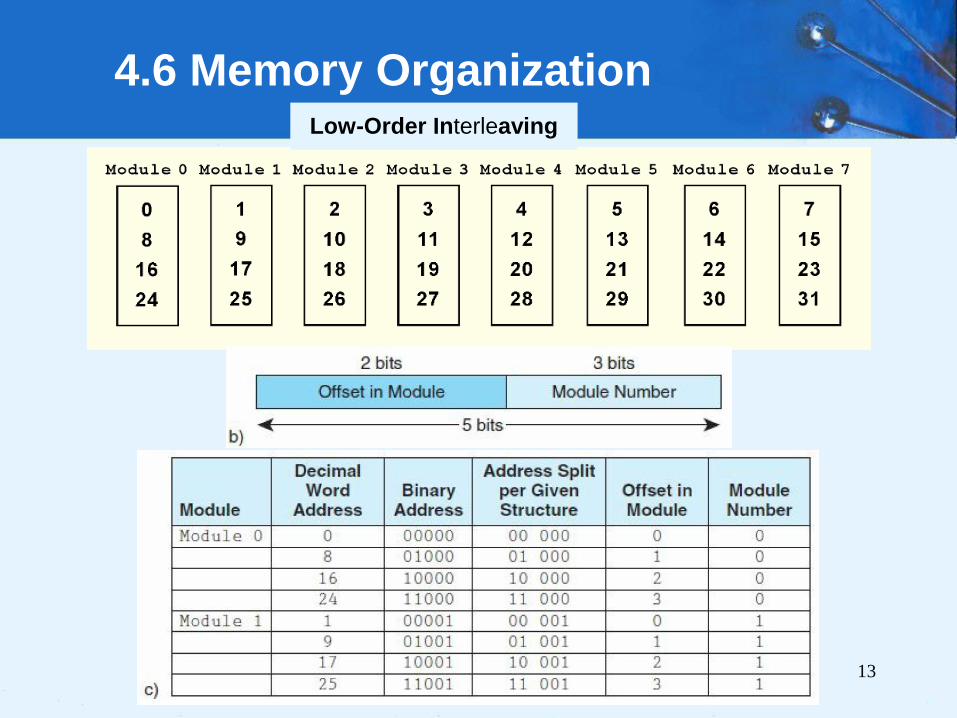
Low-Order Interleaving
4.6 Memory Organization

4.6 Memory Organization
14
High-Order Interleaving

15
4.7 Interrupts
Interrupts are events that alter (or interrupt) the normal
flow of execution in the system.
➢An interrupt from a variety of reasons, including:
– I/O requests
– Arithmetic errors (e.g., division by 0)
– Arithmetic underflow or overflow
– Hardware malfunction (e.g., memory parity error)
– User-defined break points (such as when debugging a program)
– Page faults (this is covered in detail in Chapter 6)
– Invalid instructions (usually resulting from pointer issues)
– Miscellaneous
4.7 Interrupts
The actions performed for each of these types
of interrupts (called interrupt handling) are
very different.• Interrupts can be triggered by I/O requests,
arithmetic errors (such as division by zero), or
when an invalid instruction is encountered.
• Interrupt can be initiated by the user or the system:
• maskable (disabled or ignored) or
• nonmaskable are high-priority interrupts that cannot be
ignored.
16
17
4.8 MARIE
MARIE, Machine Architecture that is Really Intuitive
and Easy, is a simple architecture consisting of:
• memory (to store programs and data)
• CPU (consisting of an ALU and several
registers).
• It has all the functional components necessary
to be a real working computer.
18
4.8 MARIE
The MARIE architecture has the following
characteristics:• Binary, two's complement data representation.
• Stored program, fixed word length
• Word (but not byte) addressable
• 4K words of word-addressable main memory.
• 16-bit data words.
• 16-bit instructions, 4 for the opcode and 12 for the
address.
• A 16-bit accumulator (AC)
• A 16-bit instruction register (IR)
19
4.8 MARIE
MARIE’s seven registers are:
• Accumulator, AC, a 16-bit register that holds a
conditional operator (e.g., "less than") or one operand
of a two-operand instruction.
• Memory address register, MAR, a 12-bit register that
holds the memory address of an instruction or the
operand of an instruction.
• Memory buffer register, MBR, a 16-bit register that
holds the data after its retrieval from, or before its
placement in memory.
20
4.8 MARIE
MARIE’s seven registers are:
• Program counter, PC, a 12-bit register that holds the
address of the next program instruction to be
executed.
• Instruction register, IR, which holds an instruction
immediately preceding its execution.
• Input register, InREG, an 8-bit register that holds data
read from an input device.
• Output register, OutREG, an 8-bit register, that holds
data that is ready for the output device.
21
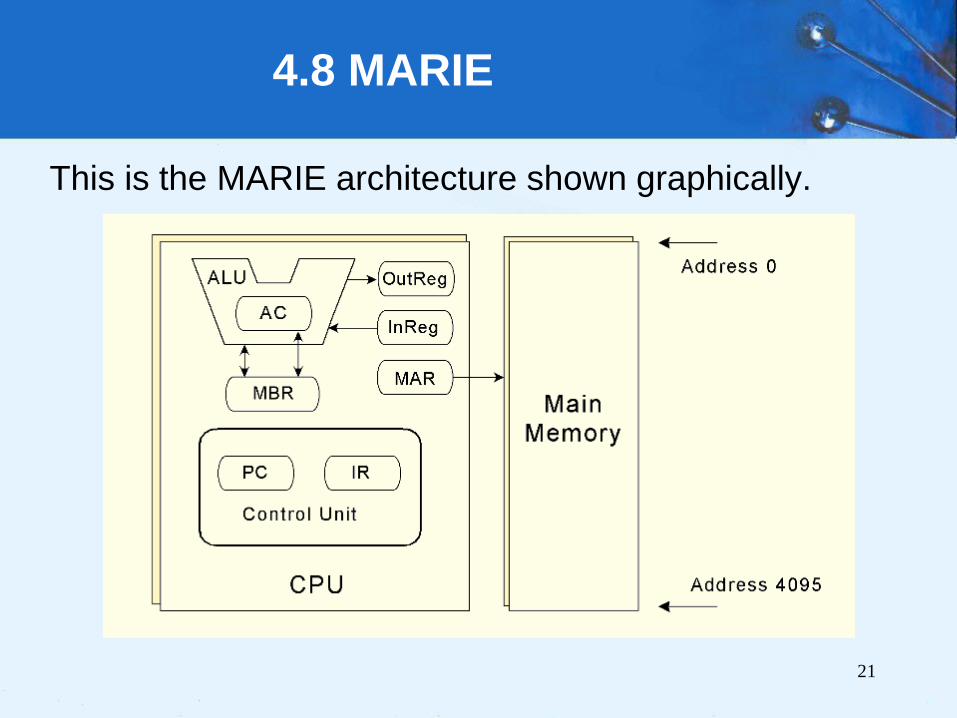
4.8 MARIE
This is the MARIE architecture shown graphically.
22
4.8 MARIE
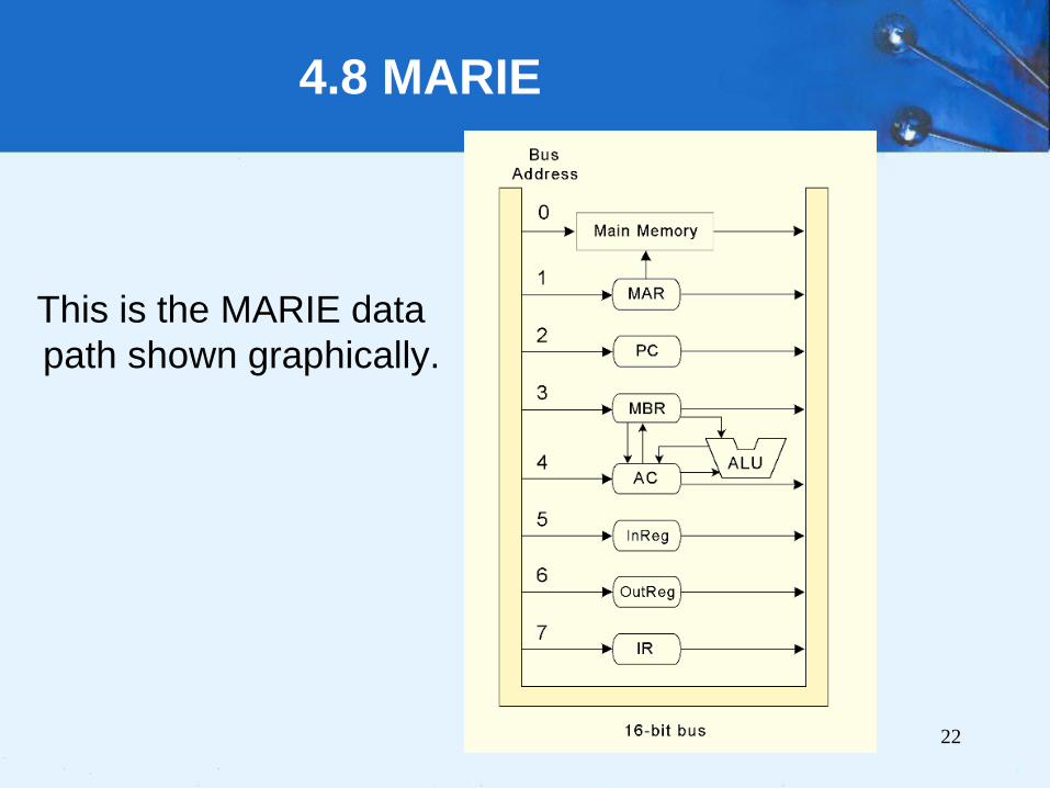
This is the MARIE data
path shown graphically.
23
4.8 MARIE
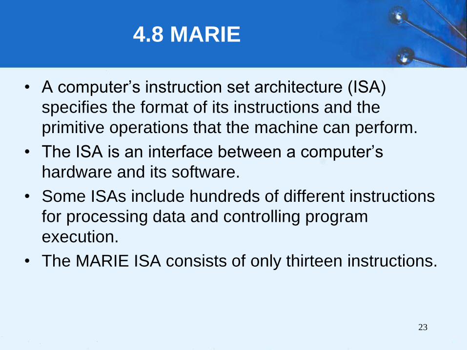
• A computer’s instruction set architecture (ISA)
specifies the format of its instructions and the
primitive operations that the machine can perform.
• The ISA is an interface between a computer’s
hardware and its software.
• Some ISAs include hundreds of different instructions
for processing data and controlling program
execution.
• The MARIE ISA consists of only thirteen instructions.
24
4.8 MARIE
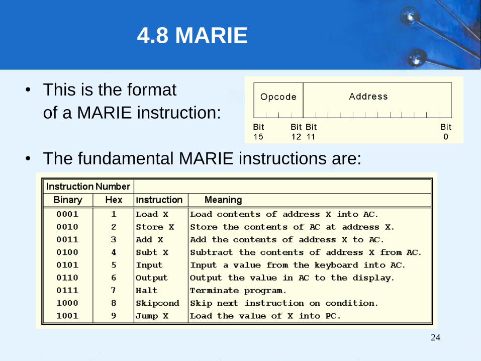
• This is the format
of a MARIE instruction:
• The fundamental MARIE instructions are:
25
4.8 MARIE
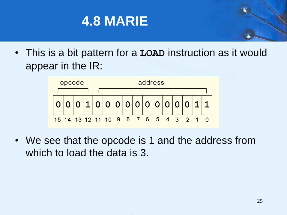
• This is a bit pattern for a LOAD instruction as it would
appear in the IR:
• We see that the opcode is 1 and the address from
which to load the data is 3.

26
4.8 MARIE
• This is a bit pattern for a SKIPCOND instruction as it
would appear in the IR:
• We see that the opcode is 8 and bits 11 and 10 are
10, meaning that the next instruction will be skipped if
the value in the AC is greater than zero.
What is the hexadecimal representation of this instruction?
27
4.8 MARIE
Register Transfer Notation
• Each of our instructions actually consists of a
sequence of smaller instructions called
microoperations.
• The exact sequence of microoperations that are
carried out by an instruction can be specified using
register transfer language (RTL).
• In the MARIE RTL, we use the notation M[X] to
indicate the actual data value stored in memory
location X, and to indicate the transfer of bytes to a
register or memory location.
28
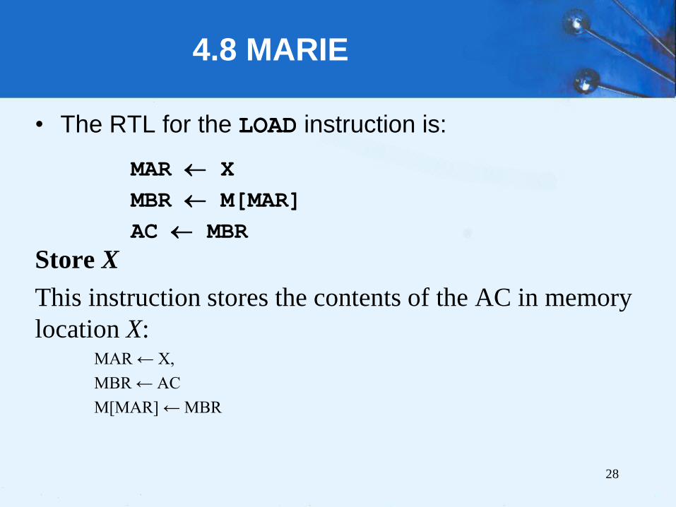
4.8 MARIE
• The RTL for the LOAD instruction is:
Store X
This instruction stores the contents of the AC in memory
location X:MAR ← X,
MBR ← AC
M[MAR] ← MBR
MAR X
MBR M[MAR]
AC MBR
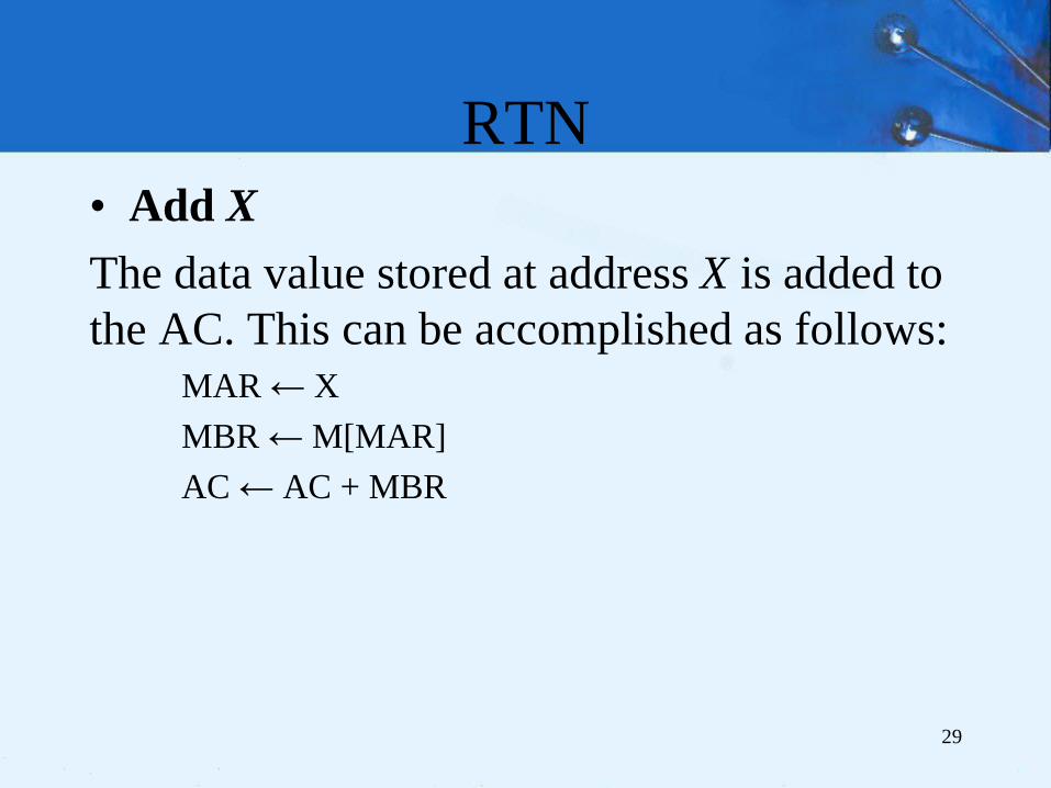
RTN
• Add X
The data value stored at address X is added to
the AC. This can be accomplished as follows:MAR ← X
MBR ← M[MAR]
AC ← AC + MBR
29
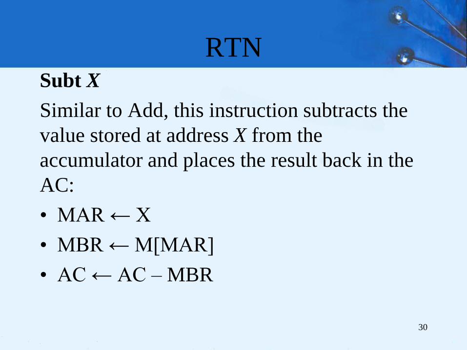
RTNSubt X
Similar to Add, this instruction subtracts the
value stored at address X from the
accumulator and places the result back in the
AC:
• MAR ← X
• MBR ← M[MAR]
• AC ← AC – MBR
30
RTNInput
Any input is put into the InREG. Then the data is
transferred into the AC.
AC ← InREG
Output
Data in AC to be placed into the OutREG, where it is
eventually sent to the output device.
OutREG ← AC
Halt
No operations are performed on registers; the machine
simply ceases execution of the program.31
32
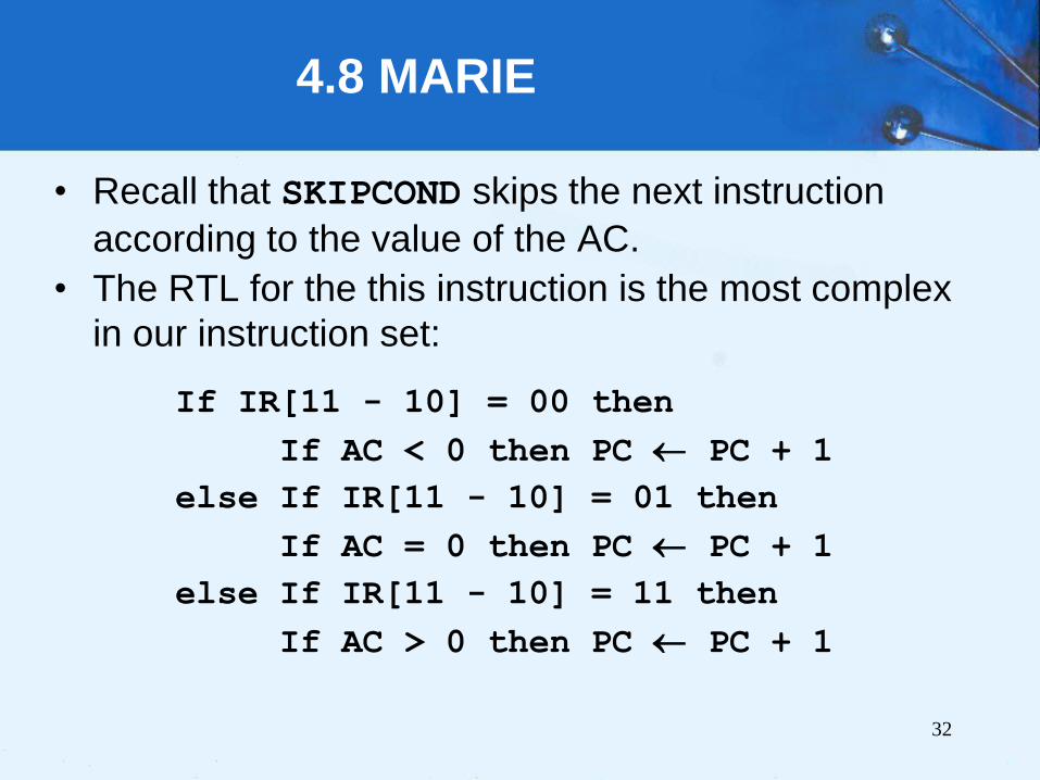
4.8 MARIE
• Recall that SKIPCOND skips the next instruction
according to the value of the AC.
• The RTL for the this instruction is the most complex
in our instruction set:
If IR[11 - 10] = 00 then
If AC < 0 then PC PC + 1
else If IR[11 - 10] = 01 then
If AC = 0 then PC PC + 1
else If IR[11 - 10] = 11 then
If AC > 0 then PC PC + 1
RTN
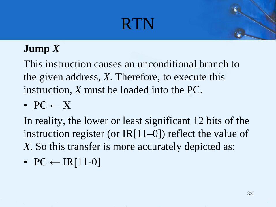
Jump X
This instruction causes an unconditional branch to
the given address, X. Therefore, to execute this
instruction, X must be loaded into the PC.
• PC ← X
In reality, the lower or least significant 12 bits of the
instruction register (or IR[11–0]) reflect the value of
X. So this transfer is more accurately depicted as:
• PC ← IR[11-0]
33
34
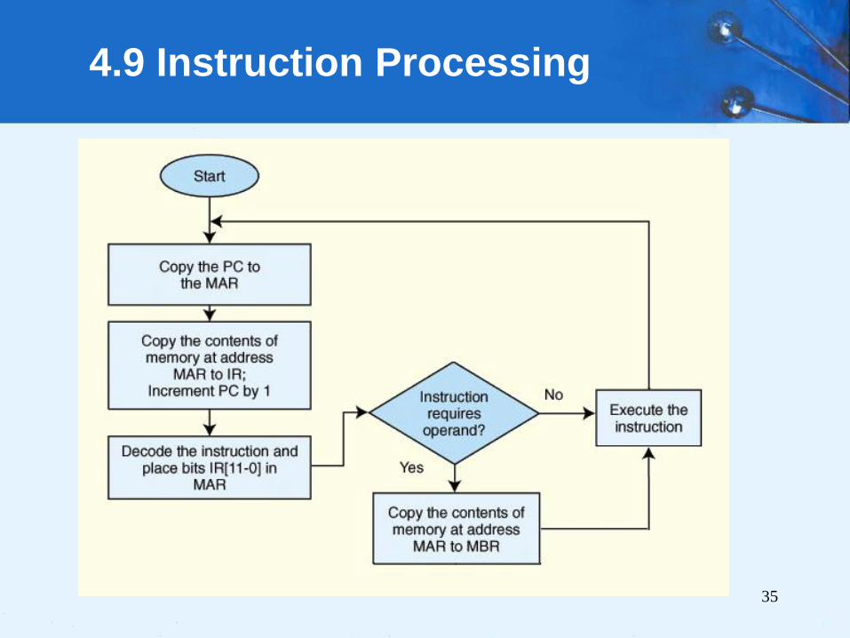
4.9 Instruction Processing
• fetch-decode-execute cycle is the series of steps that
a computer carries out when it runs a program.
• Fetch, an instruction from memory, and place it into
the IR.
• Opcode in IR is decoded to determine what needs to
be done next.
• If the instruction needs the operand, it is retrieved
and placed into the MBR.
• With everything in place, the instruction is executed.
The next slide shows a flowchart of this process.
35
4.9 Instruction Processing
36
4.9 Instruction Processing
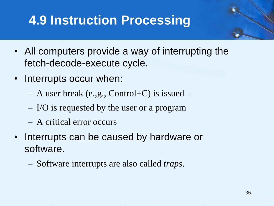
• All computers provide a way of interrupting the
fetch-decode-execute cycle.
• Interrupts occur when:
– A user break (e.,g., Control+C) is issued
– I/O is requested by the user or a program
– A critical error occurs
• Interrupts can be caused by hardware or
software.
– Software interrupts are also called traps.
37
4.9 Instruction Processing
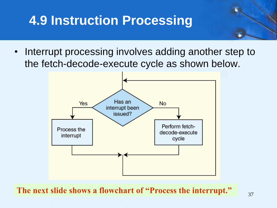
• Interrupt processing involves adding another step to
the fetch-decode-execute cycle as shown below.
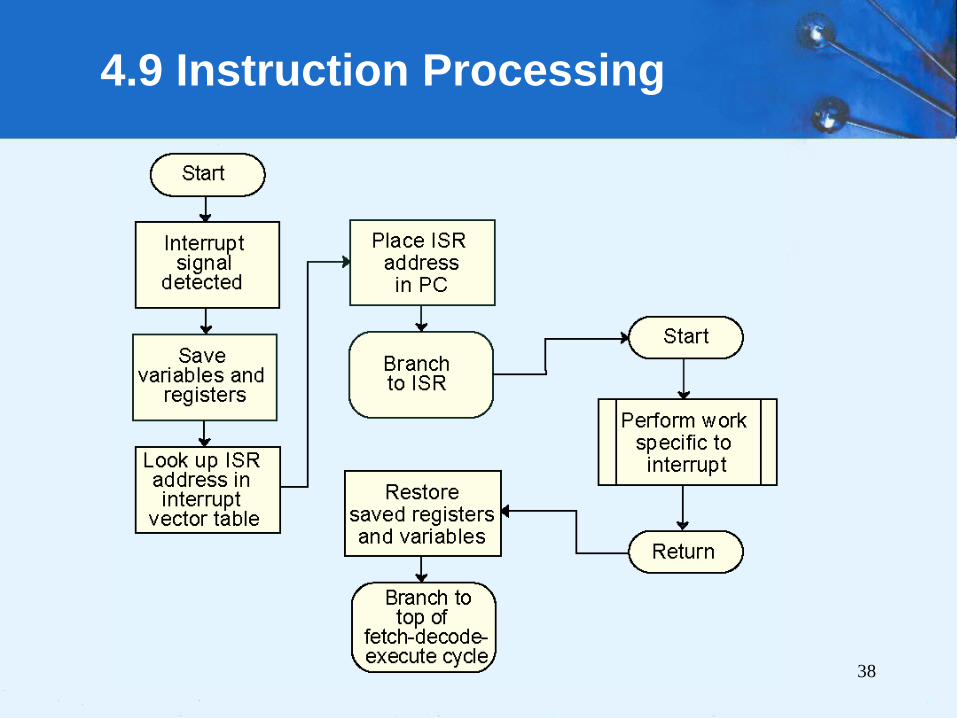
The next slide shows a flowchart of “Process the interrupt.”
38
4.9 Instruction Processing
39
4.9 Instruction Processing
• For general-purpose systems, it is common to
disable all interrupts during the time in which an
interrupt is being processed.
– Typically, this is achieved by setting a bit in the flags
register.
• Interrupts that are ignored in this case are called
maskable.
• Nonmaskable interrupts are those interrupts that
must be processed in order to keep the system in
a stable condition.
40
4.9 Instruction Processing
• Interrupts are very useful in processing I/O.
• However, interrupt-driven I/O is complicated, and
is beyond the scope of our present discussion.
– We will look into this idea in greater detail in Chapter 7.
• MARIE, being the simplest of simple systems,
uses a modified form of programmed I/O.
• All output is placed in an output register, OutREG,
and the CPU polls the input register, InREG, until
input is sensed, at which time the value is copied
into the accumulator.
41
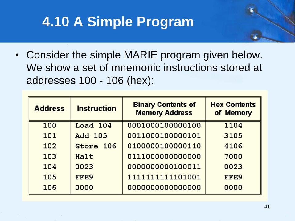
• Consider the simple MARIE program given below.
We show a set of mnemonic instructions stored at
addresses 100 - 106 (hex):
4.10 A Simple Program
42
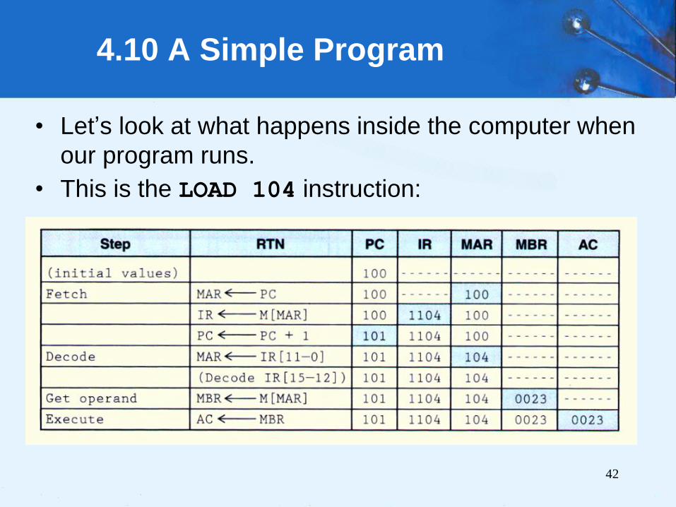
• Let’s look at what happens inside the computer when
our program runs.
• This is the LOAD 104 instruction:
4.10 A Simple Program
43
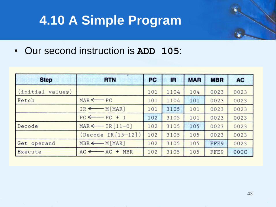
• Our second instruction is ADD 105:
4.10 A Simple Program
4.10 A Simple Program
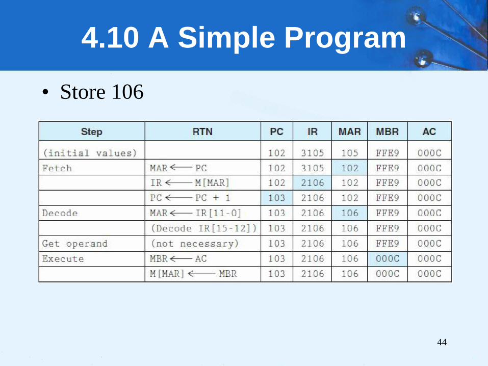
• Store 106
44
45
4.11 A Discussion on Assemblers
• Mnemonic instructions, such as LOAD 104, are easy
for humans to write and understand.
• They are impossible for computers to understand.
• Assemblers translate instructions that are
comprehensible to humans into the machine
language that is comprehensible to computers
– The distinction between an assembler and a compiler: In
assembly language, there is a one-to-one correspondence
between a mnemonic instruction and its machine code. With
compilers, this is not usually the case.
46
• Assemblers create an object program file from
mnemonic source code in two passes.
• During the first pass, the assembler assembles as
much of the program is it can, while it builds a
symbol table that contains memory references for
all symbols in the program.
• During the second pass, the instructions are
completed using the values from the symbol table.
4.11 A Discussion on Assemblers
47
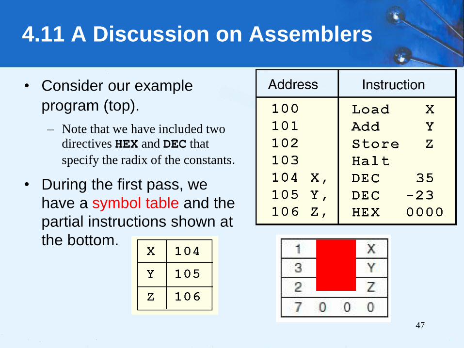
• Consider our example
program (top).
– Note that we have included two directives HEX and DEC that
specify the radix of the constants.
• During the first pass, we
have a symbol table and the
partial instructions shown at
the bottom.
4.11 A Discussion on Assemblers

48
• After the second pass, the
assembly is complete.
4.11 A Discussion on Assemblers
49
4.12 Extending Our Instruction Set
• So far, all of the MARIE instructions that we have
discussed use a direct addressing mode.
• This means that the address of the operand is
explicitly stated in the instruction.
• It is often useful to employ a indirect addressing,
where the address of the address of the operand is
given in the instruction.
– If you have ever used pointers in a program, you are
already familiar with indirect addressing.

50
• What happens at the machine level, we have
included an indirect addressing mode instruction to
the MARIE instruction set.
• ADDI instruction specifies the address of the
address of the operand. RTL tells us what is
happening at the register level:
MAR X
MBR M[MAR]
MAR MBR
MBR M[MAR]
AC AC + MBR
4.12 Extending Our Instruction Set
51
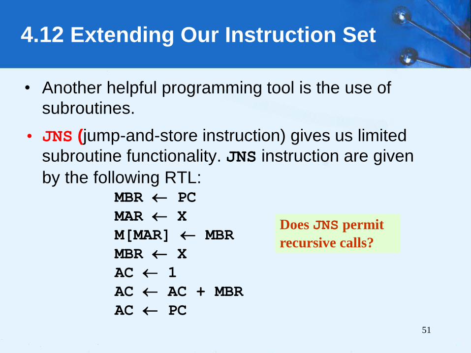
• Another helpful programming tool is the use of
subroutines.
• JNS (jump-and-store instruction) gives us limited
subroutine functionality. JNS instruction are given
by the following RTL: MBR PC
MAR X
M[MAR] MBR
MBR X
AC 1
AC AC + MBR
AC PC
Does JNS permit
recursive calls?
4.12 Extending Our Instruction Set

52
• CLEAR instruction.
• All it does is set the contents of the accumulator to
all zeroes.
• This is the RTL for CLEAR:
• We put our new instructions to work in the program
on the following slide.
AC 0
4.12 Extending Our Instruction Set
53
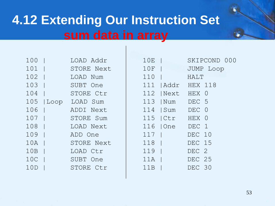
100 | LOAD Addr
101 | STORE Next
102 | LOAD Num
103 | SUBT One
104 | STORE Ctr
105 |Loop LOAD Sum
106 | ADDI Next
107 | STORE Sum
108 | LOAD Next
109 | ADD One
10A | STORE Next
10B | LOAD Ctr
10C | SUBT One
10D | STORE Ctr
10E | SKIPCOND 000
10F | JUMP Loop
110 | HALT
111 |Addr HEX 118
112 |Next HEX 0
113 |Num DEC 5
114 |Sum DEC 0
115 |Ctr HEX 0
116 |One DEC 1
117 | DEC 10
118 | DEC 15
119 | DEC 2
11A | DEC 25
11B | DEC 30
4.12 Extending Our Instruction Set
sum data in array
54
4.12 Extending Our Instruction Set
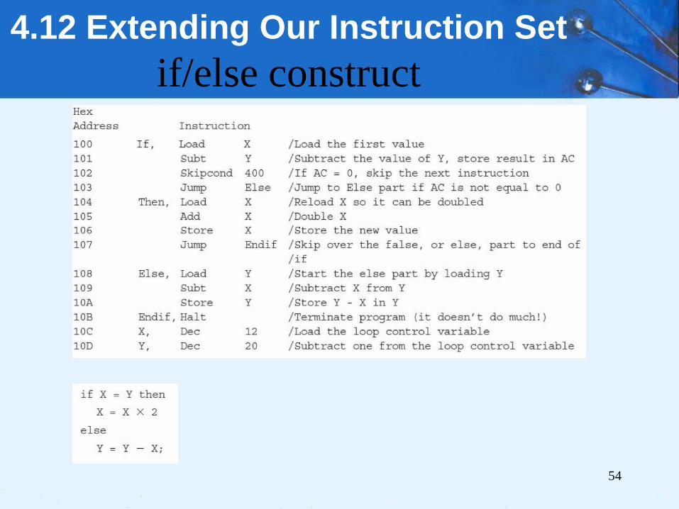
if/else construct
4.12 Extending Our Instruction Set
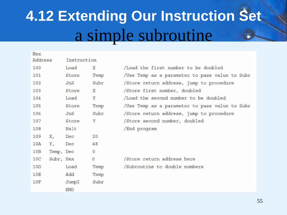
a simple subroutine
55
56
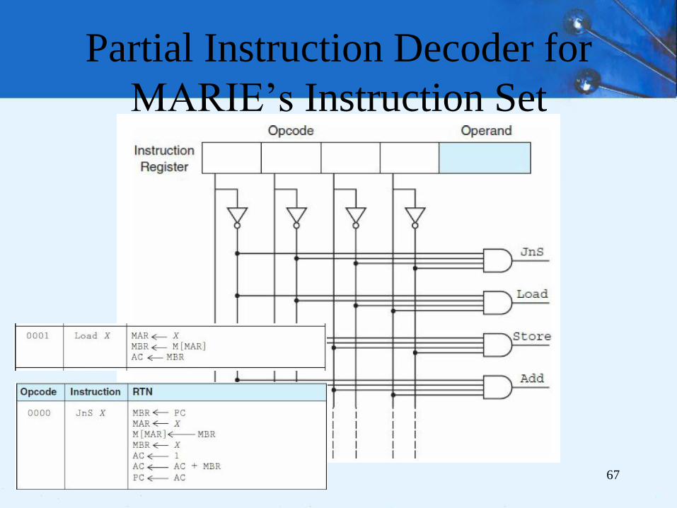
4.13 A Discussion on Decoding
• Control unit keeps things synchronized, making sure
that bits flow to the correct components as the
components are needed.
• Control unit can be implemented: hardwired control
and microprogrammed control.
– With microprogrammed control, a small program is placed
into ROM in the microcontroller.
– Hardwired controllers implement this program using digital
logic components.
57
4.13 A Discussion on Decoding
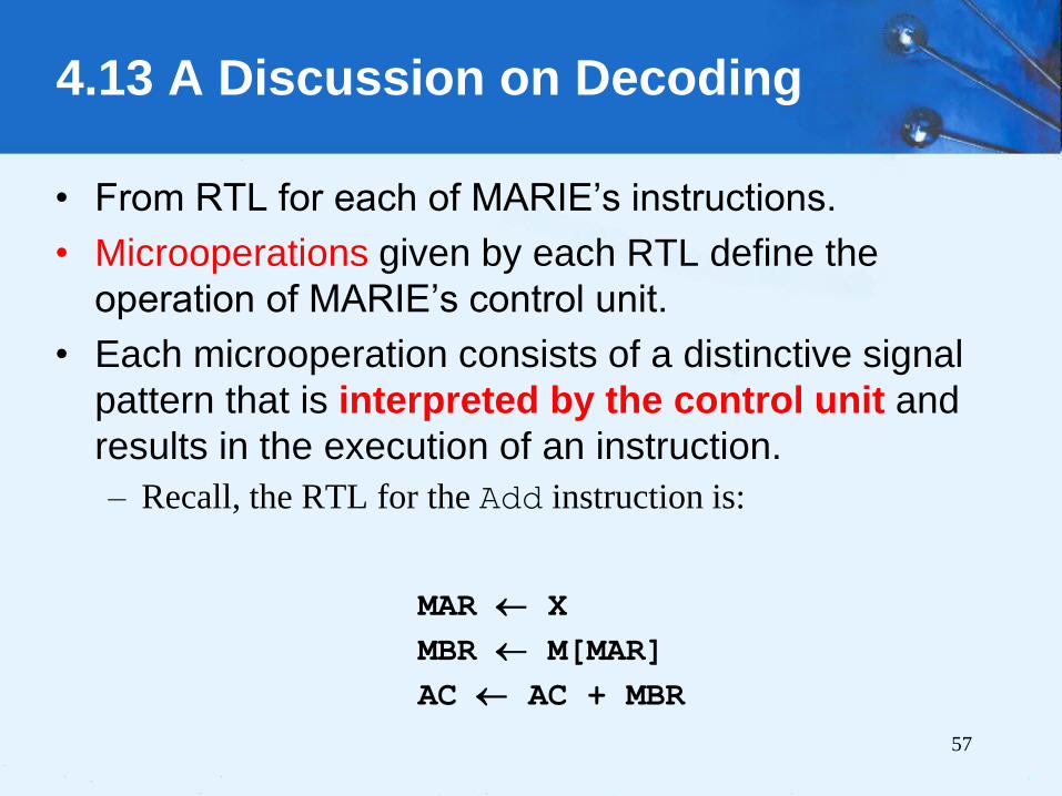
• From RTL for each of MARIE’s instructions.
• Microoperations given by each RTL define the
operation of MARIE’s control unit.
• Each microoperation consists of a distinctive signal
pattern that is interpreted by the control unit and
results in the execution of an instruction.
– Recall, the RTL for the Add instruction is:
MAR X
MBR M[MAR]
AC AC + MBR
58
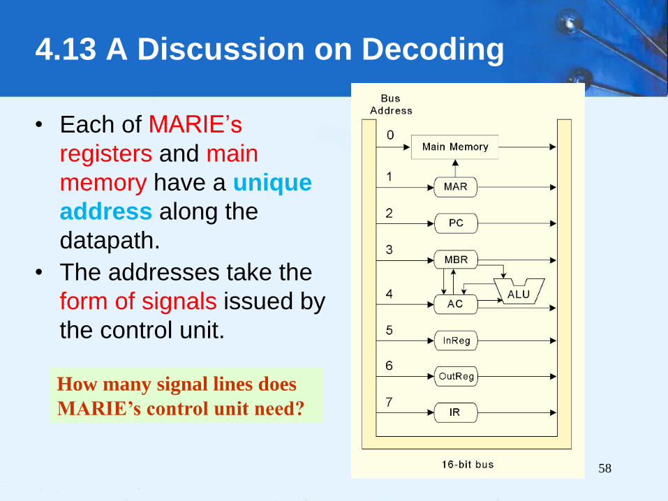
4.13 A Discussion on Decoding
• Each of MARIE’s
registers and main
memory have a unique
address along the
datapath.
• The addresses take the
form of signals issued by
the control unit.
How many signal lines does
MARIE’s control unit need?
59
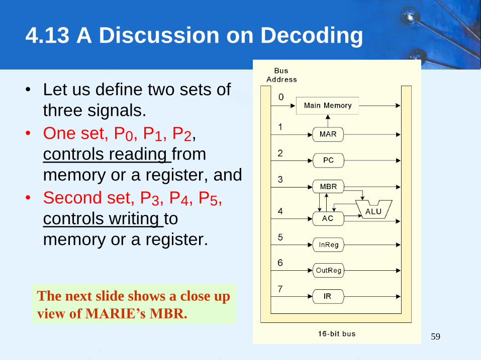
4.13 A Discussion on Decoding
• Let us define two sets of
three signals.
• One set, P0, P1, P2,
controls reading from
memory or a register, and
• Second set, P3, P4, P5,
controls writing to
memory or a register.
The next slide shows a close up
view of MARIE’s MBR.
60
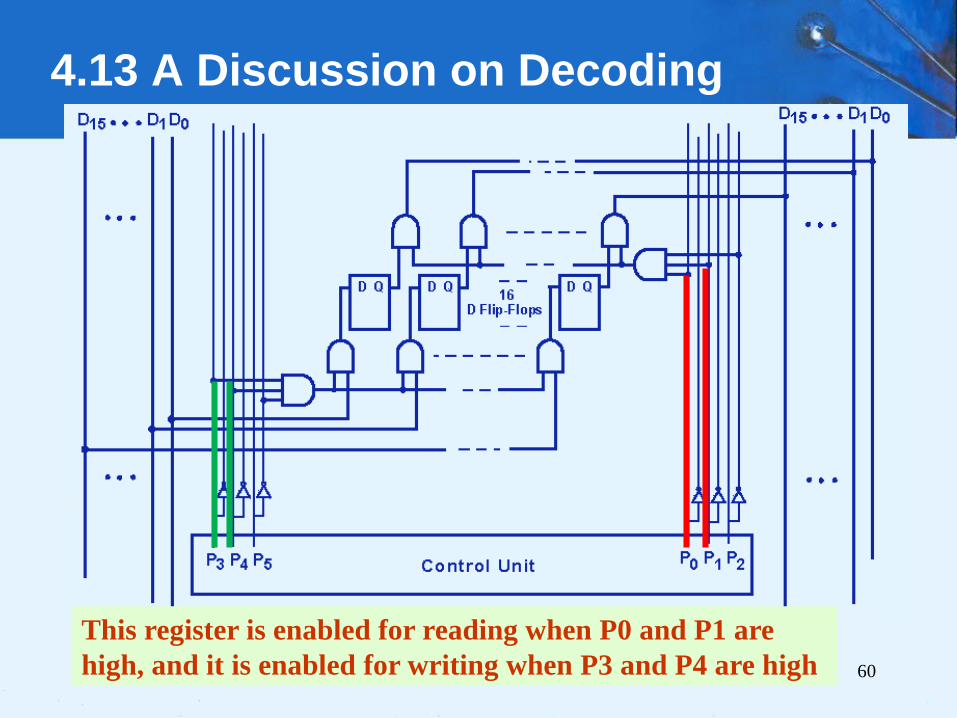
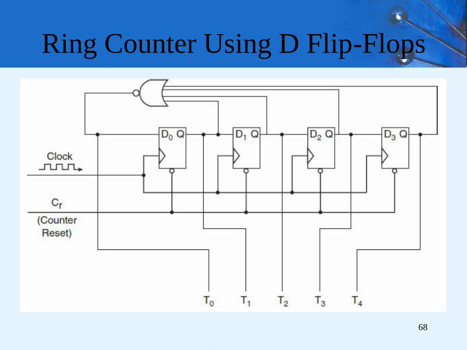
4.13 A Discussion on Decoding
This register is enabled for reading when P0 and P1 are
high, and it is enabled for writing when P3 and P4 are high
61
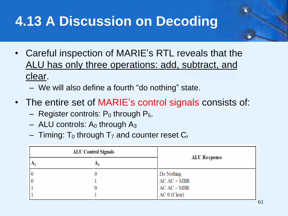
4.13 A Discussion on Decoding
• Careful inspection of MARIE’s RTL reveals that the
ALU has only three operations: add, subtract, and
clear.– We will also define a fourth “do nothing” state.
• The entire set of MARIE’s control signals consists of:– Register controls: P0 through P5.
– ALU controls: A0 through A3
– Timing: T0 through T7 and counter reset Cr
62
4.13 A Discussion on Decoding
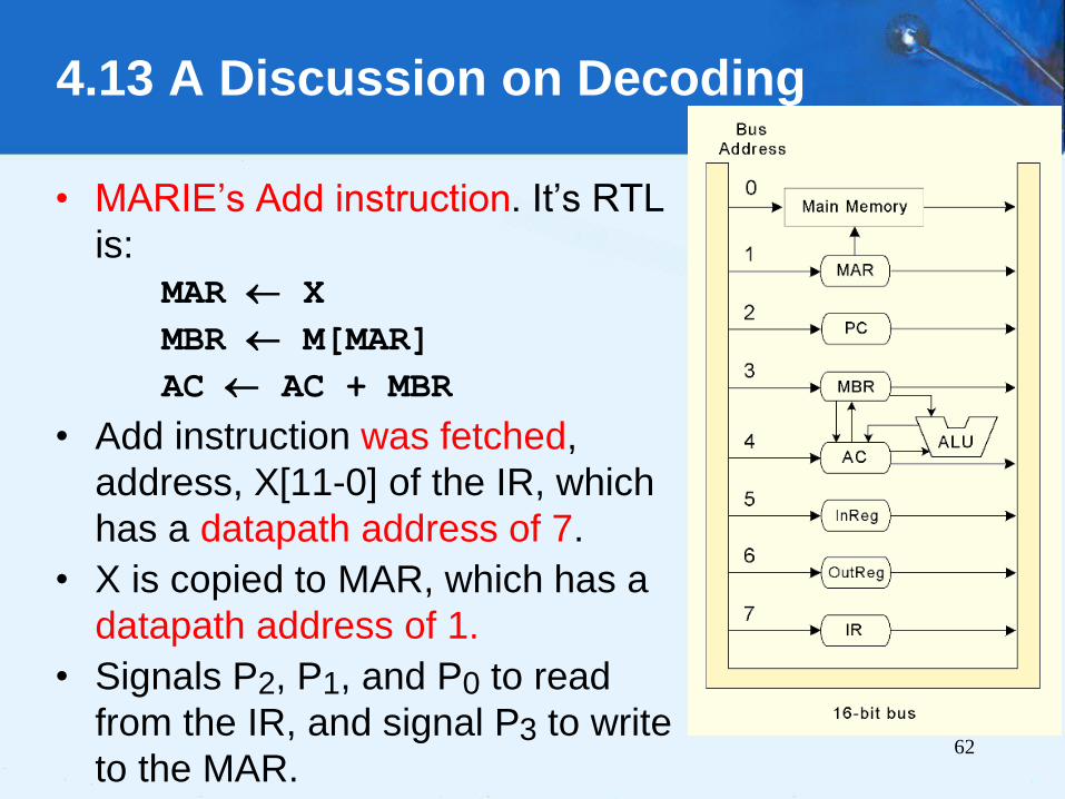
• MARIE’s Add instruction. It’s RTL
is:MAR X
MBR M[MAR]
AC AC + MBR
• Add instruction was fetched,
address, X[11-0] of the IR, which
has a datapath address of 7.
• X is copied to MAR, which has a
datapath address of 1.
• Signals P2, P1, and P0 to read
from the IR, and signal P3 to write
to the MAR.
63
4.13 A Discussion on Decoding
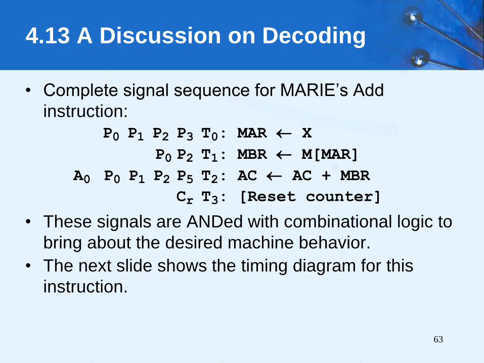
• Complete signal sequence for MARIE’s Add
instruction:P0 P1 P2 P3 T0: MAR X
P0 P2 T1: MBR M[MAR]
A0 P0 P1 P2 P5 T2: AC AC + MBR
Cr T3: [Reset counter]
• These signals are ANDed with combinational logic to
bring about the desired machine behavior.
• The next slide shows the timing diagram for this
instruction.
64
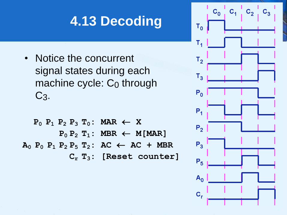
4.13 Decoding
P0 P1 P2 P3 T0: MAR X
P0 P2 T1: MBR M[MAR]
A0 P0 P1 P2 P5 T2: AC AC + MBR
Cr T3: [Reset counter]
• Notice the concurrent
signal states during each
machine cycle: C0 through
C3.
65
4.13 A Discussion on Decoding
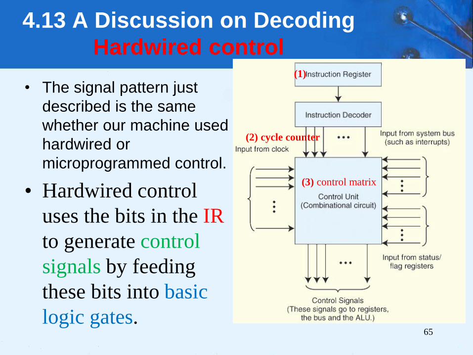
Hardwired control
• The signal pattern just
described is the same
whether our machine used
hardwired or
microprogrammed control.
• Hardwired control
uses the bits in the IR
to generate control
signals by feeding
these bits into basic
logic gates.
(1)
(2) cycle counter
(3) control matrix
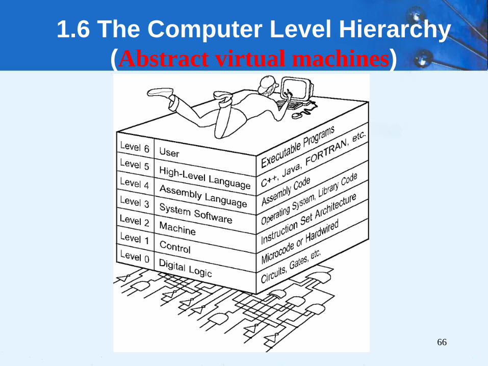
1.6 The Computer Level Hierarchy
(Abstract virtual machines)
66
Partial Instruction Decoder for
MARIE’s Instruction Set
67
Ring Counter Using D Flip-Flops
68
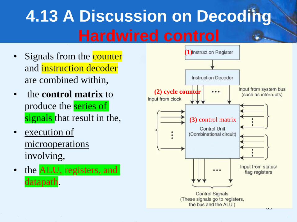
4.13 A Discussion on Decoding
Hardwired control• Signals from the counter
and instruction decoder
are combined within,
• the control matrix to
produce the series of
signals that result in the,
• execution of
microoperations
involving,
• the ALU, registers, and
datapath.
69
(1)
(2) cycle counter
(3) control matrix
70
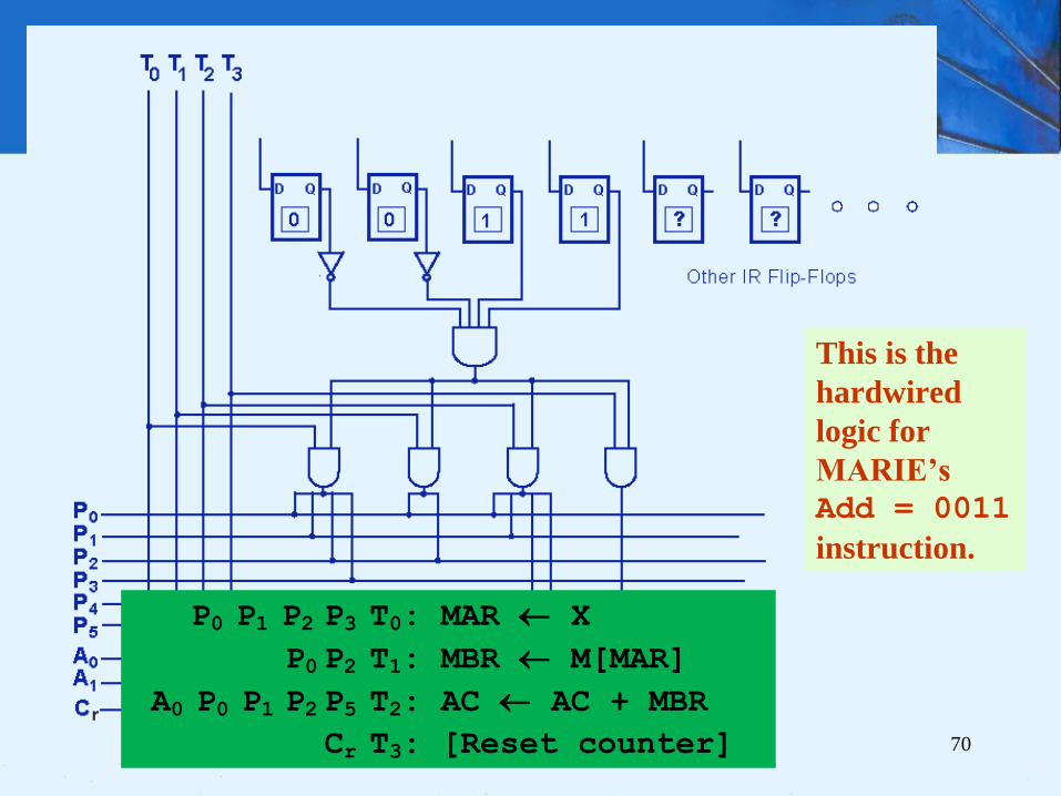
4.13 A Discussion on Decoding
This is the
hardwired
logic for
MARIE’s
Add = 0011
instruction.
P0 P1 P2 P3 T0: MAR X
P0 P2 T1: MBR M[MAR]
A0 P0 P1 P2 P5 T2: AC AC + MBR
Cr T3: [Reset counter]
71
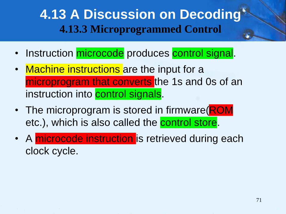
4.13 A Discussion on Decoding4.13.3 Microprogrammed Control
• Instruction microcode produces control signal.
• Machine instructions are the input for a
microprogram that converts the 1s and 0s of an
instruction into control signals.
• The microprogram is stored in firmware(ROM
etc.), which is also called the control store.
• A microcode instruction is retrieved during each
clock cycle.
72
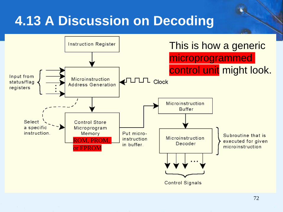
4.13 A Discussion on Decoding
This is how a generic
microprogrammed
control unit might look.
ROM, PROM,
or EPROM

73
• If MARIE were microprogrammed, the
microinstruction format might look like this:
• MicroOp1 and MicroOp2 contain binary codes for
each instruction. Jump is a single bit indicating that
the value in the Dest field is a valid address and
should be placed in the microsequencer.
4.13 A Discussion on Decoding

74
RTN for the fetch–decode–
execute cycle• There are only 22 unique microoperations
to implement MARIE’s entire instruction
set.
• Two additional microoperations:
– NOP, “no operation” is useful when the system
must wait for a set of signals to stabilize, when
waiting for fetching from memory.
– Compares the bit (IR[15–12]) to a literal value
that is in the first 4 bits of the MicroOp2 field.
75

76
• The table below contains MARIE’s microoperation
codes along with the corresponding RTL:
4.13 A Discussion on Decoding
77
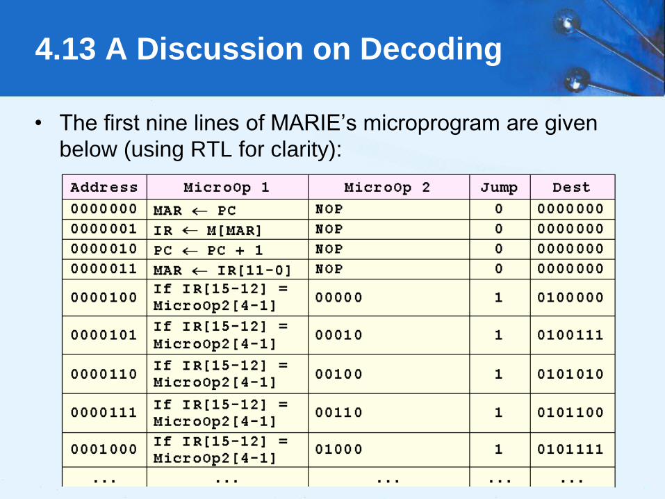
• The first nine lines of MARIE’s microprogram are given
below (using RTL for clarity):
4.13 A Discussion on Decoding
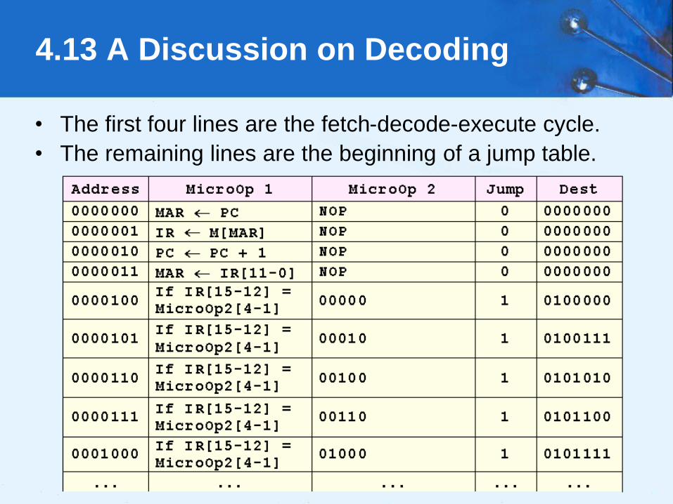
78
• The first four lines are the fetch-decode-execute cycle.
• The remaining lines are the beginning of a jump table.
4.13 A Discussion on Decoding
79
• A microprogrammed control unit works like a system
in miniature.
• To fetch an instruction from the control store, a
certain set of signals must be raised.• This extra level of instruction interpretation is what
makes microprogrammed control slower than
hardwired control.
• The advantages of microprogrammed control are that
it can support very complicated instructions and only
the microprogram needs to be changed if the
instruction set changes (or an error is found).
4.13 A Discussion on Decoding

80
4.14 Real World Architectures
• MARIE shares many features with modern
architectures but it is not an accurate depiction of
them.
• In the following slides, we briefly examine two
machine architectures.
• We will look at an Intel architecture, which is a CISC
machine and MIPS, which is a RISC machine.
– CISC is an acronym for complex instruction set computer.
– RISC stands for reduced instruction set computer.
We delve into the “RISC versus CISC” argument in Chapter 9.
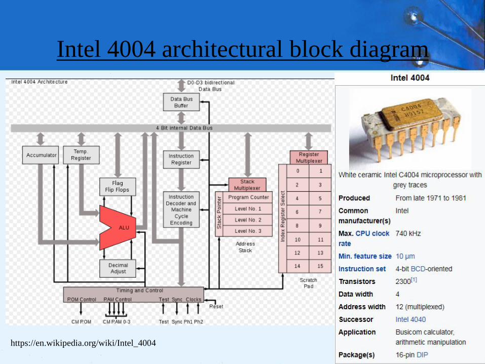
Intel 4004 architectural block diagram
81https://en.wikipedia.org/wiki/Intel_4004
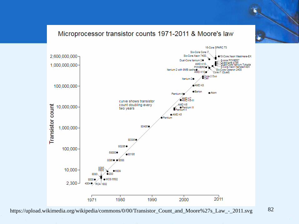
82https://upload.wikimedia.org/wikipedia/commons/0/00/Transistor_Count_and_Moore%27s_Law_-_2011.svg
83
4.14 Real World Architectures
• The classic Intel architecture, the 8086, was born in
1979. It is a CISC architecture.
• It was adopted by IBM for its famed PC, which was
released in 1981.
• The 8086 operated on 16-bit data words and
supported 20-bit memory addresses.
• Later, to lower costs, the 8-bit 8088 was
introduced. Like the 8086, it used 20-bit memory
addresses.
What was the largest memory that the 8086 could address?
84
4.14 Real World Architectures
• The 8086 had four 16-bit general-purpose registers
that could be accessed by the half-word.
• It also had a flags register, an instruction register,
and a stack accessed through the values in two
other registers, the base pointer and the stack
pointer.
• The 8086 had no built in floating-point processing.
• In 1980, Intel released the 8087 numeric
coprocessor, but few users elected to install them
because of their cost.
85
4.14 Real World Architectures
• In 1985, Intel introduced the 32-bit 80386.
• It also had no built-in floating-point unit.
• The 80486, introduced in 1989, was an 80386 that
had built-in floating-point processing and cache
memory.
• The 80386 and 80486 offered downward
compatibility with the 8086 and 8088.
• Software written for the smaller word systems was
directed to use the lower 16 bits of the 32-bit
registers.
86
4.14 Real World Architectures
• Intel’s most advanced 32-bit microprocessor is the
Pentium 4.
• It can run as fast as 3.8 GHz. This clock rate is
nearly 800 times faster than the 4.77 MHz of the
8086.
• Speed enhancing features include multilevel cache
and instruction pipelining.
• Intel, along with many others, is marrying many of
the ideas of RISC architectures with
microprocessors that are largely CISC.
87
4.14 Real World Architectures
• MIPS family, CPUs has been one of the most
successful in its class.
• In 1986 the first MIPS CPU was announced.
• It had a 32-bit word size and could address 4GB of
memory.
• Over the years, MIPS processors have been used in
general purpose computers as well as in games.
• The MIPS architecture now offers 32- and 64-bit
versions.
88
4.14 Real World Architectures
• MIPS was one of the first RISC microprocessors.
• Original MIPS architecture had only 55 different
instructions, as compared with the 8086 which had
over 100.
• MIPS was designed with performance in mind: It is a
load/store architecture, meaning that only the load
and store instructions can access memory.
• The large number of registers in the MIPS
architecture keeps bus traffic to a minimum.
How does this design affect performance?

89
• The major components of a computer system
are its control unit, registers, memory, ALU, and
data path.
• A built-in clock keeps everything synchronized.
• Control units can be microprogrammed or
hardwired.
• Hardwired control units give better performance,
while microprogrammed units are more
adaptable to changes.
Chapter 4 Conclusion
90
• Computers run programs through iterative fetch-
decode-execute cycles.
• Computers can run programs that are in
machine language.
• An assembler converts mnemonic code to
machine language.
• The Intel architecture is an example of a CISC
architecture; MIPS is an example of a RISC
architecture.
Chapter 4 Conclusion

91
End of Chapter 4