Embed Size (px)
Citation preview
-
Chapter 4
Modified Technique for Deposition of CuInSez Thin Films Using
Sequential Elemental Evaporation and Characterization
4.1 Introduction
In the last chapter, an economical and eco-friendly method was demonstrated for the
deposition of CulnSe2 (CIS) thin films in whieh chemically deposited Selenium was
used. Optimization of these CulnSe2 films was carried out and with this optimized
sample, an attempt to device fabrication was also made. Here CdS was the buffer layer.
But photovoltaic effect could not be observed with this CulnSe2/CdS junction. One of the
possible reasons for this could have been the reduced thickness of the absorber layer,
which was < O.S~un. For the fabrication of solar cells, thickness of the absorber layer
should be greater than 0.5 ~lIn in order to have efficient absorption of the solar radiation,
even though theoretical calculation predicts efficiency above 17% for an optimized cell
with a thickness of 0.3 ~lIn.1 The main draw back of the above mentioned deposition
technique was that the thickness of the Se layer could not be increased above a cer1ain
limit. As the thickness goes beyond this limit, the films star1cd to peel off Hence the
overall thickness of the CuInSe2 films, prepared using Se layer deposited using CBO
technique, was limited to less than 0.5~lIn.
With the aim of fabricating a solar cell with bctter efficiency, a modified techniquc was
developed using vacuum evaporation. whereby the film thickness could be increased. In
literature, there are many reports on deposit ion of Cui nSc" th in films using vacuum
evaporatioll. ~.(, I nterestingly. the record-hreaking 19.9(Yo eftic ient cell \\ as a Iso fabricated
Using co-cvapnration tcclllliqu<.:." In all tilL: rL:ported kchniqllc.~. Cll. In and Se were
Modified technique for deposition of CulnSe2 thin films using... 110
deposited either in elemental or in compound form, at very high substrate temperatures
starting from 350°C. Moreover, these processes are complex and controlling the
deposition parameters is also difficult. In the present work, CulnSe2 thin films were
deposited through sequential evaporation of Se, In and Cu, at moderately low substrate
temperature. This method of sequential evaporation is simpler than co-evaporation
technique and control of stoichiometry could be easily achieved. We could deposit highly
stoichiometric samples through this method. Here we made an attempt to deposit sub
micrometre thick absorber layers and tabricate solar cells lIsing these.
The key issues in the field of CulnSe2 based solar cells are, reducing the thickness of CIS
and the replacement of CdS with non-toxic and low absorbing materials. Typical
absorber layer thickness of today's solar'cell ranges between 2 to 3~Lm. Reducing the
thickness of the absorber layer is one of the challenges to minimize the processing time
and material usage, particularly of Indium. Work is going on to replace Indium partially
by Ga, AI etc. The main reasons to find an altemative buffer layer are the following:
(a) The expected environmental risks arising from implementation of a CBO CdS
process in a CIGS module production linc could be avoided.
(b) The expected technological problcms caused by a non-vacuum CBO process in a
vacuum line could be separated.
(c) The potcntial of increasing current generation in the spectral region of 350-550 nm,
and thereby increasing the cell efficiency is another possibility.
(d) As the presence of Cadmium in electrical or electronic equipment has already been
prohibited through legal regu lations in difterent countries, there is a marketing
problem for the Cd-containing CIGS-based thin-film modules today.
In2S1, ZnS, ZnO, ZnSe, In2Se" InZnSe" SnSl, Sn02 are repOlted to be the possible
alternative butler layers for CIS solar cells. In the present work, we chose In1S3 prepared
through 'cht:mical spray pyrolysis' as the buffer layer. This was Cl novel approach as
CulnSecl In2S, junctions. This is rather rare as 1110st of the rt:ports are on the devices
prepared lIsing vaellum c\aroratioll technique for the entire cell.

,apter 4 111 -.4J Experimental details , . soda lime glass was used as the substrate in this work. Samples were prepared using
tbennal evaporation of Cu, In and Se at a pressure of 10-5
mbar. Quantity of Cu, In and Se
to be evaporated was selected such that the film stoichiometry was I: I :2. Rates of
evaporation were 0.5 nm/sec, 0.3 nm/sec and 0.2 nm/sec for Se, In and ClI respectively.
After deposition, the samples were annealed at 400°C for one hour at a pressure of 10-5
IJlbar resulting in the formation ofCulnSc2.
4.3 Optimization of deposition process
Molybdenum (Mo) coated glass (thickness of Mo ~- 80 A) was llsed as the substrate in the
optimization work. The Mo substrate was highly resistive so that it did not affect the
conductivity measurements of the CIS sample. The deposition process was optimized by
varying parameters like, substrate temperature, annealing rate and the sequence in which
the three layers were deposited. As a primary step, deposition was carried out by
sequential evaporation of Se, In and Cll to get the structurc of glass/Mo/Se/fn/Cu,
keeping the substratc at room temperature. This sample was named as CIS I. After
deposition, the sample was annealed at 400°C lhcating rate -2.5°ClminJ for one hour at a
pressure of 10-5 mbar resulting in the formation of CulnSe2.
A point to be noticed in this course is that an intermediate annealing at 1500 e (near the
melting point of In) was carried out for these samples, before increasing the temperature
to 400°(:. This process helped to form eu-In alloy and subsequent selenization of this
alloy lead to formation of euI nSe2.
From the X-ray ditfractogram of CIS I (Fig 4. I), single phase CuinSe2 with chalcopyrite
structure was identified. Peaks were at angles 29= 17.1 0, 26.6°, 35.45°, 44.02°, 52.32°,
64.32° and 70.8° respectively. On comparing tll\,; observed cl-spacing with powder
diffraction standards (.JCPDS card 23-209), planes were identified as (103) at 28=17.1°,
(112) at 26.6", (211) at 35.45", (220)i(204) a144.0Y (116)/(312) at 52.3". (400) at 65.02"
and (316) al 71.51 ". The sample showed strong, preferential orientation along (112) plane.
The charactcri.~lic chalcopyrite peaks \\en: obtained at (103). (211) and (400) planes.
~p'.waJf,elt technique for deposition of CulnSe2 thin films using... 112
CISl
10 20 30 40 50 60 70
Angle (20) Degree.
Fig.4.1: X-ray diffractogram ofCIS 1
Grain size was calculated lIsing Debye-Scherrer's formula s, and was found to be of the
order of 45 nm. However the samples were found to be highly porous in nature to the
naked eye. Five samples of dimension 3 .5x I cm2 were prepared at a time. Among these, at
least four were showing similar XRD pattern in spite of being porous in appearance. This
proved that the structural propcI1ies were repeatable in this type of preparation.
In order to reduce the porosity, the deposition process was repeated by reducing the
annealing temperature to 300°C (sample CIS2) keeping all the other deposition
parameters identical to that used for sample CISl. XRD pattern of sample annealed at
300°C is given in fig 4.2. It showed that reduction in annealing temperature lead to the
formation of InSe phase together with CulnSe2 phase.
The peak at 23.3 0 was corresponding to InSe phase (JCPDS card27-0244). Moreover, on
reducing the annealing temperature to 300°C, porous nature of the film did not change
and resulted in the decrcase of crystallinity compared to the samples annealed at 400°C.
The temperature of 400°C has been reported to be the optimum temperature for the
deposition ofelS by many authors. 'i. 10
rChapter4 113 -CISZ
10 20 30 40 50 60 7D
An gip. 211 degree.
Fig.4.2: X-ray ditTractogram ofCIS2
In the next trial, Se was deposited at a substrate temperature of 50°C, while In and Cu
layers were deposited at room temperature, followed by annealing of the entire structure
at 400°C at a pressure of 2x J 0-5 mbar and this set of samples was named as Cl S3. Visual
examination revealed reduction in the porosity of the film. With the increase in substrate
temperature, the surface mobility of the adsorhed species increased because of which
they interacted among themselves, resulting in continuous tilms with well-dctined grains
of large size.
As the next step, samples were prepared by keeping the deposition parameters identical to
that of CIS3, but changing the heating rate \vhile annealing at 40QoC. The heating rate
was reduced to 1.2°C Iminute ti'om 2.5°C Iminute. These samples were named as ClS4.
Crystallinity of the sample also improved slightly. But these were stiiJ showing porous
nature. Fig 4.3 reveals the XRD pattern of samples CIS3 and CIS4 which clearly showed
that CIS3 was a better polycrystalline sample compared to CIS4.
MOdified technique for deposition of CulnSe2 thin films using... 114
fi c
CIS3
f ~ ~
oD tJ,
!J IG'
f a
~ .!i
CIS4
~-~.~~, :::::::::;::::, ::'~~, ~~, :=:;=~, ==1 10 'If 311 "0 50 liD iD IQ
An~. (2 U) d • .,. •• ,
Fig 4.3: CIS3 X-ray diffractograms of and CIS4
The deposition process was further modified by depositing 'In' first at a substrate
temperature of 100°C, followed by Se at 50°C and Cu at room temperature. Such samples
[named as C1S5] exhibited better crystallinity without the porous nature. This might be
due to the enhanced surface mobility of the adsorbed In atoms which tilled the voids.
Grain size increased to 60 nm even though this value was less compared to that already
reported. Only three prom inent peaks were observed corresponding to planes (112) at 29
= 26.6°, (220)/(204) at 44.10 and (116)/(312) at 52.30 respectively (fig 4.4). The
characteristic chalcopyrite peaks were absent in these samples.
JII 2U '" 4" 5" 00 7!1 BU
Angle (29) degree.
Fig.4.4: X-ray diffractograll1 of CIS5
thapter4 115 ....... ,
I : Following the same deposition process as that of sample CIS5, deposition was repeated
without keeping the samples at 150°C for one hOllr during the annealing process. These
were named as CrS6. Fig 4.5 shows the XRD spectra of these. The sample sho\ved the
same polycrystalline quality as that of CIS5, with grain size of 57 nm. This is almost
equal to that of CISS. Hence it was concluded that, when 'In' was evaporated at a
substrate temperature of 100°C, intermediate annealing at 150°C was not required. This
could save time during deposition, making this method easier. Hence this method was
followed for further fabrication process. This process was repeated to check consistency
in the results and the properties of the repeated sample showed negligible variations.
----------
CIS6
~ Q
I:!. :;:.. :;l I:!.
~ 0-
to 20 30 40 50 60 70 80 Angle (20) degrees
Fig.4.5: X-ray diffractogram ofClS6
To evaluate the degree of crystallinity of these samples, Preferred Orientation Quality
(POQ ilkl) in the (hkl) direction was calculated lIsing the formula 11;
POQ = . 111kl ilkl ~
~ llIkl (FWHM HI Ri hkl ) (4.1 )
"'d
where I Ilk I is the actual intensity of the diffracting line hkl, FWHM ilk! is their full width at
half maximulll and Ri ilk! is the relative intensity of that particular line. ill a p(mder
sample. POQ was calculated for all samples and the values are given in table 4.1.
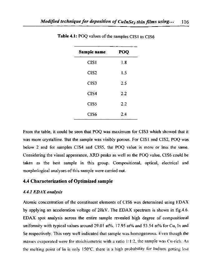
Modified technique for deposition ofCulnSez thin films using... 116
Table 4.1: POQ values of the samples CISl to CIS6
Sample name POQ
CISI 1.8
CIS2 1.5
CIS3 2.5
CIS4 2.2
CIS5 2.2
CIS6 2.4
From the table, it could be seen that POQ was maximum for CIS3 which showed that it
was more crystalline. But the sample was visibly porous. For CIS 1 and CIS2, POQ was
below 2 and for samples CIS4 and CIS5, the POQ value is more or less the same.
Considering the visual appearance, XRD peaks as well as the POQ value, CIS6 could be
taken as the best sample in this group. Compositional, optical, electrical and
morphological analyses of this sample were carried out.
4.4 Characterization of Optimized sample
4.4.1 EDAX analysis
Atomic concentration of the constituent elements of CIS6 was detennined using EDAX
by applying an acceleration voltage of 20kV. The EDAX spectrum is shown in fig.4.6.
EDAX spot analysis across the entire sample revealed high degree of compositional
unifonnity with typical values around 29.01 at%. 17.95 at% and 53.54 at% for Cu. In and
Se respectively. This very well indicated that sample was homogeneolls. Even though the
masses evaporated were for stoichiometric with a ratio I: I :2, the sample was ClI-rich. As
the melting point of In is only 150°(', there is a high probability for Indilllll getting lost
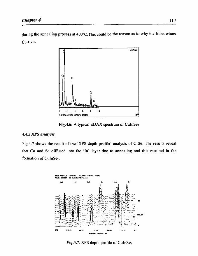
Chapter 4 117
during the annealing process at 400oC.This could be the reason as to why the films where
eu-rich.
Sja:fnml
Cl .,
Cl
~ ~~'1. Cl LA...
J ".
"s 8 10 f.JSc8lel07m CIlS«OI.OOkeV ~
Fig.4.6: A typical EDAX spectrum of CuInSe2
4.4.2 XPS analysis
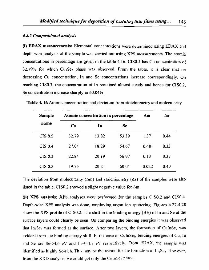
FigA.7 shows the result of the 'XPS depth profile' analysis of CIS6. The results reveal
that Cu and Se diffused into the 'In' layer due to annealing and this resulted in the
formation ofCuinSe2'
IleA NGI"lLl 101l/0! 1U&1W2. DD-JZ 1 .,...2 nU:.QI22J1 CZ CUlftWftto./Gl ...
no 9254'0 .uooo ~05U 5212112 2201114
Fig.4.7: XPS depth profile ofClllnSe~
..
Modified technique for deposition of CuInSe2 thin films using... 118
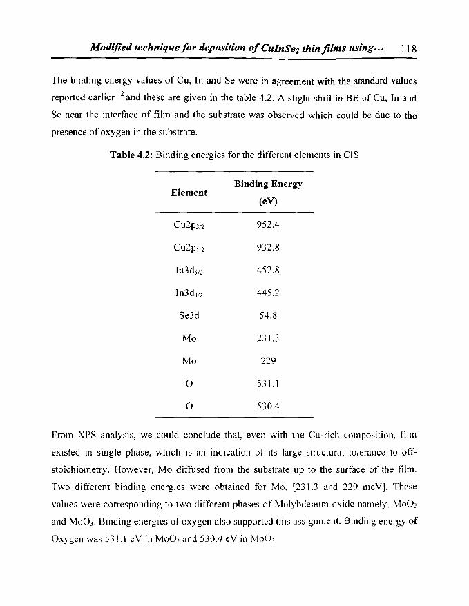
The binding energy values of Cu, In and Se were in agreement with the standard values
rep011ed earlier 12 and these are given in the table 4.2. A slight shift in BE of Cu, In and
Se near the interface of film and the substrate was observed which could be due to the
presence of oxygen in the sl1bstrate.
Table 4.2: Binding energies for the different elements in CIS
Element Binding Energy
(eV)
CU2P3i2 952.4
CU2pli2 932.8
In3dsi2 452.8
In3d3/2 445.2
Se3d 54.8
Mo 231.3
Mo 229
0 531.1
0 530.4
From XPS analysis, we could conclude that, even with the Cu-rich composition, film
existed in single phase, which is an indication of its large structural tolerance to off
stoichiometry. However, Mo diffused from the substrate up to the surface of the film.
Two different binding energies were obtained for Mo, [231.3 and 229 meV]. These
values were corresponding to two different phases of Molybdenum oxide namely, MoO]
and MoO). Binding energies of oxygen also supp011ed this assignment. Binding energy of
Oxygen was 531.1 eV in MoO] and 530.4 cV in MoO.l.

thapter4 119 -4.4.3 Thickness measurement
Film thickness and sample surface roughness were determined from the one dimensional
scan carried out by means of Dektak32 stylus profilometer. Thickness of the sample was
found to be 0.79 I.un while the average roughness was 93.6 nm. Thickness can be
increased by multi layer deposition, if required.
4.4.4 Optical absorption
Absorption spectrum was recorded in the wavelength range 500 nm to 1500 nm for all
the samples. Fig 4.8 shows the plot of (ahv)2 versus hv for sample CTS6.
[ ~lJ.97 e\' , 1.11
O.II+------_""""'~--......,---...J i I
Fig.4.8: Absorption spectra of ClI] nSe2
Band gap obtained, by extrapolating the linear portion of the (ahv)2 versus hv graph to
hv axis [0.97 eV], was close to the reported value for Cu-rich films \3. In all the films,
there existed a second absorption edge at energy ~ 1.1 cV. This absorption is attributed to
the 'valence band splitting', a phenomenon commonly
sem iconductors.
occurrill" ill b 1-llI- VI 2
The valence band of CIS consists of three sub-bands. i\t the top. there is a hroad band
built up from Sc-4p and ell-3d states. Next is a nalTO\\Cr band formed from Ill-SS and Se-
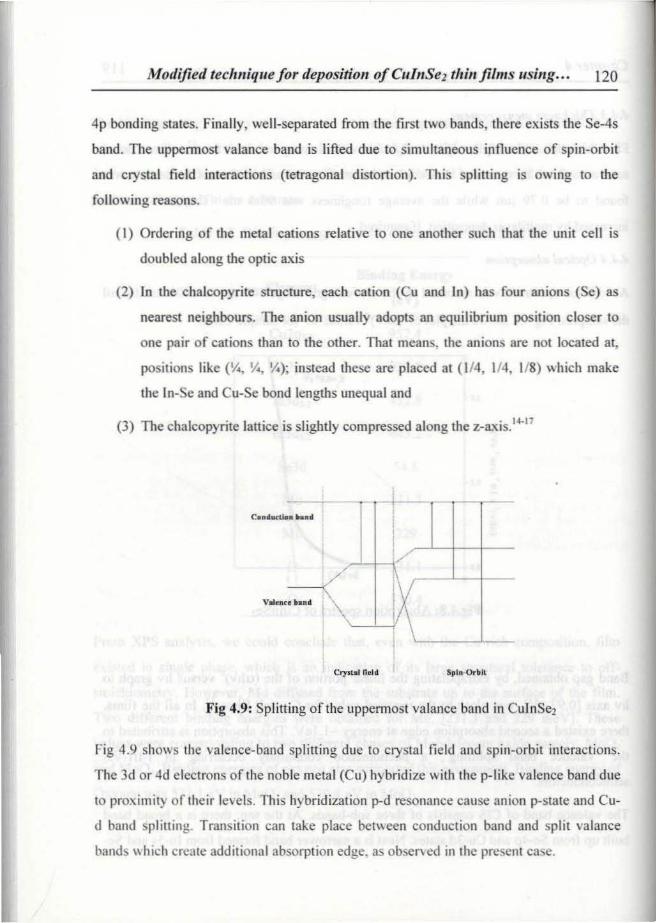
.Uodified technique for deposition ofClII" Sez thin films using, s, 120
4p bonding states. f inally, well-separated from the first two bands. there ex ists the Se-s s
band. The uppe rmost valance band is lifted due to simultaneous influence of spin-orbit
and crystal field interactions (tetragonal distort ion). This splitting is owing to the
following reasons.
( 1) Ordering of the metal cat ions relative 10 one another such that the unit cell IS
doub led along the opt ic axis
(2) In the chalcopyrite structure, each cation (Cu and In) has four anions (Se) as
nearest neighbours. The anion usually adopts an equilibrium posit ion close r to
one pair of cations than to the othe r. Thai means. the anions are not located at,
positions like (1/., Y•• Yo ); instead these are placed at (1/4, 1/4, 1/8) which make
the In-Se and Cu-Se bond lengths unequa l and
(3) The cbalcopyrite lattice is slightly compressed a long the z-axts." :"
- - --...... IIII:../"'
~ i\ I
I
Fig 4.9: Splitting of the uppermost valance band in CulnSc2
Fig 4.9 shows the va lence-band splitting due to crystal field and spin-orbit interactions.
The 3d or 4d electrons of the noble meta l (Cu ) hybridize with the p-like va lence band due
10 proxim ity of the ir levels. Thi s hybridization p-d resonance cause anion p-state and Cu
d band splitt ing. Tran sition can take place between co nduction band and split va lance
hands which create additional absorption edge. as observed in the present case.
thapter4 121 -4.4.5 Electrical characterization
Hot probe measurement confirmed the samples to be p-type. Generally p-type samples
are eu-rich 18 and this was consistent with EDAX measurement. Resistivity of the sample
was found to be 3 Qcm, from the dark I-V characteristics. For fabrication of solar cells,
resistivity of the order of 10 Qcm is usually preferred. The resistivity could be varied by
varying the composition in the tilm.
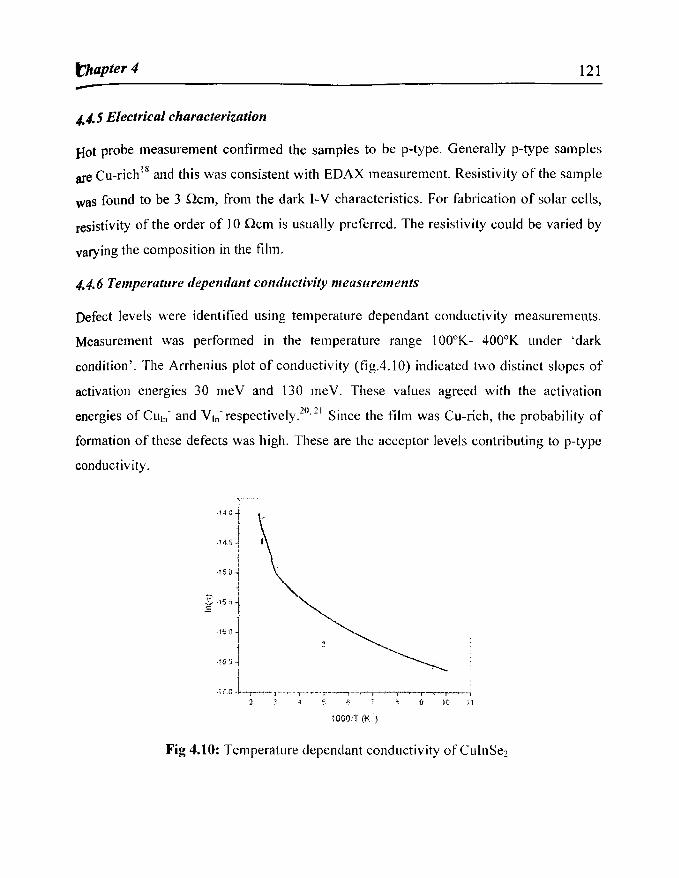
4.4.6 Temperature dependant conductivity measurements
Defect levels were identified lIsing temperature dependant conductivity measurements.
Measurement was performed in the temperature range 100oK- 4000K under 'dark
condition'. The Arrhenius plot of conductivity (fig.4.1 0) indicated two distinct slopes of
activation energies 30 meY and 130 meV. These values agreed with the activation
energies of CUln- and V ln- respectively.2O, 21 Since the film was Cu-rich, the probability of
formation of these defects was high. These are the acceptor levels contributing to p-typc
conductivity.
.1-10
.145
-l~> 0
-1 r.e '~-r'·t-l···~· . Y··-··;-·-··'--!···-~r"-"j"· I~""''''''' -·r--,.,........"'l 2 ~ ~ HI;1
100QfT (I< )
Fig 4.10: Temperature dependant conductivity ofCulnSe2
Modified technique for deposition of CulnSe] thin films using.. . 122 -4.4.7 Morphological analysis
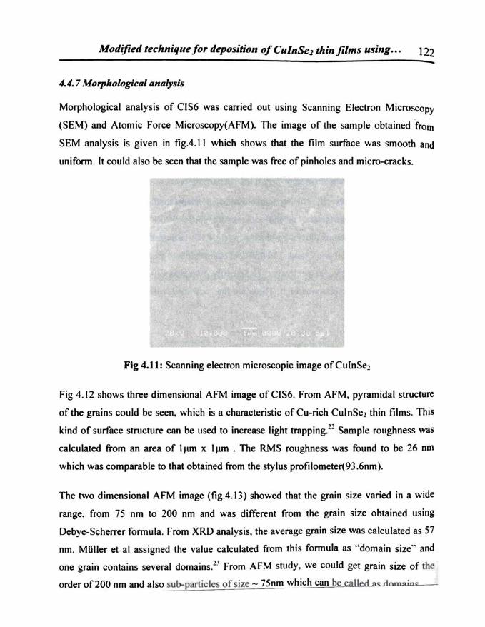
Morphological analysis of CIS6 was carried out using Scanning Electron Microscopy
(SEM) and Atomic Force Microscopy(AFM). The image of the sample obtained ·from
SEM analysis is given in fig.4 .11 which shows that tne film surface was smooth and
unifonn . It could also be seen that the sample was free of pinholes and micro-cracks.
Fig 4.11: Scanning electron microscopic image ofCulnSel
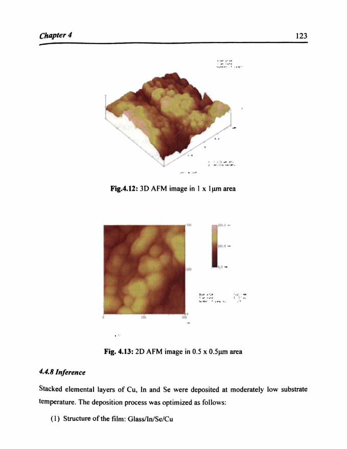
Fig 4.12 shows three dimensional AFM image ofCIS6. From AFM, pyramidal structure
of the grains could be seen, which is a characteristic of Cu·rich CuinSel thin films. This
kind of surface structure can be used to increase light trapping.l~ Sample roughness was
calculated from an area of I ~ x 1 ~ . The RMS roughness was found to be 26 nm
which was comparable to that obtained from the stylus profilometer(93.6nm).
The two dimensional AFM image (fig.4.I3) showed that the grain size varied in a wide
range. from 75 nm to 200 nm and was different from the grain size obtained using
Debye·Scherrer fonnula. From XRD analysis. the average grain size was calculated as 57
nm. Muller et al assigned the value calculated from this fonnula as "domain size" and
one grain contains several domains.1J From AFM study, we could get grain size of the
order of200 nm and also sub.particles of size - 75 nm which can be cal led a s: doma;n ..
C/ulpler 4 123 -" , ,.,.
;" ... ". ~ ,c .• ' _ ' . '.
Fig.4.12: 3D AFM image in I x IJlm area
, ... , -
.. -. -
k .. , ' ,. ". J _
' " . ," , : ....... ..... ',
Fig. 4.13: 20 AFM image in O.S x O .5~ area
4.4.8 Inference
Slacked elemental layers of Cu, In and Se were deposited at moderately low substrate
temperature. The deposition process was optimized as follows:
(I) Structure of the film : GlassllnlSe/Cu
"!JAa eVPilii,.ij6F ii!jJ3Mhan oJ CuinSel rmn films usmg... 124
(2) Indium evaporation at 100°C
(3) Selenium evaporation at 50°C
(4) Copper evaporation at room temperature
(5) Annealing this layer at 400°C
All these processes were carried out at a pressure Of 2 x 10⁻⁵ mbar. On analyzing the
characteristics of the sample, we could infer that this procedure can be followed for
further deposition. The samples were again deposited at the same condition to ensure
repeatability and the film characteristics showed nearly the same values.
Films were characterized by varying the concentration ofCu, In and Se, one at a time.
4.5 Effect of variation of Cu
CuInSe2 thin films were prepared by varying the concentration of Cu keeping In and Se
concentrations constant at 110 and 170mg respectively. Concentration of Cu was varied
from 40mg to 80mg. These samples were named as CIS7, CIS8, CIS9 and CISI0
depending up on concentration of Cu.
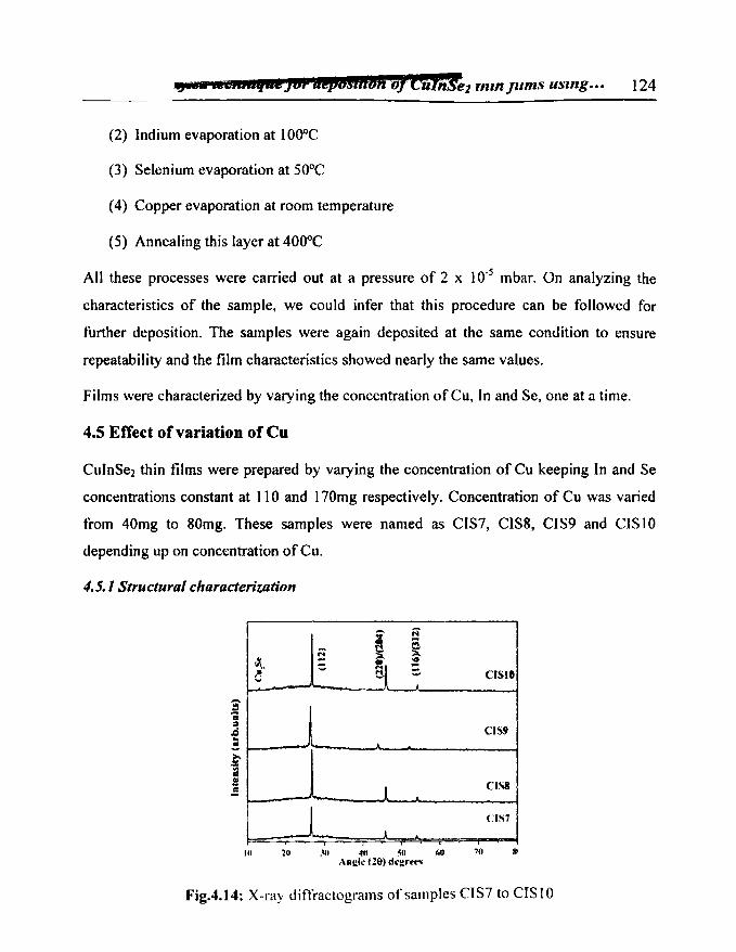
4.5.1 Structural characterization
;- M
... ~ i .)l •• ~ al ~ ~ .... ClSIO
1 CIS9
1 C1SR J..
1 C1S7
~
211 .10 411 ~8 Ml "n!ll~ (20) del!r£1.'S
Fig.4.14: X-ray diffractograms of samples CIS7 to CIS 10
Chapter 4 125
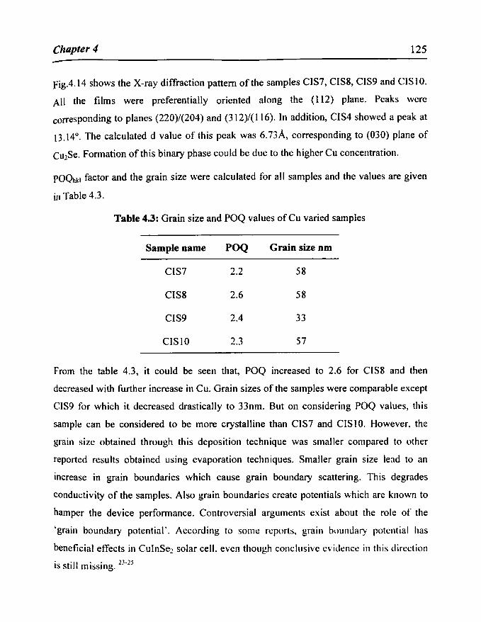
Fig.4.14 shows the X-ray diffraction pattern of the samples CIS7, CIS8, CIS9 and CIS 10.
All the films were preferentially oriented along the (112) plane. Peaks were
corresponding to planes (220)/(204) and (312)/(116). In addition, CIS4 showed a peak at
13.14°. The calculated d value of this peak was 6.73A, corresponding to (030) plane of
Cu~Se. Formation of this binary phase could be due to the higher Cu concentration.
POQ,kl factor and the grain size were calculated for all samples and the values are given
in Table 4.3.
Table 4.3: Grain size and POQ values ofCu varied samples
Sample Dame POQ Grain size om
CIS7 2.2 58
CIS8 2.6 58
CIS9 2.4 33
CISIO 2.3 57
From the table 4.3, it could be seen that, POQ increased to 2.6 for CIS8 and then
decreased with further increase in Cu. Grain sizes of the samples were comparable except
CIS9 for which it decreased drastically to 33nm. But on considering POQ values, this
sample can be considered to be more crystalline than CIS7 and CIS I O. However, the
grain size obtained through this deposition technique was smaller compared to other
reported results obtained using evaporation techniques. Smaller grain size lead to an
increase in grain boundaries which cause grain boundary scattering. This degrades
conductivity of the samples. Also grain boundaries create potentia Is which are known to
hamper the device performance. Controversial arguments exist about the role of the
'grain boundary potential'. According to some reports, grain bounual) potential has
beneficial effects in CulnSe2 solar cell. even though conclusive evidence in this direction
is still missing. 13-25
Modified tecll1lique for deposition of CulnSez thi" films usillg... 126
The calculated values of lattice constants a, band c are given in the table 4.4 and these
values were comparable with the reported ones.26 Among these, 'a' was high tor CIS9,
which had the lowest grain size. In the CIS lattice, tetragonal distortion occurs due to the
excess and def1ciency of bond charge in the In-Se and Cu-Se bonds respectively. This
results in shortening of the In-Se bond, compared to the Cu-Se bond with a cOITesponding
shift in the anion (sub-lattice displacement). The In-Se tetrahedron is consequently more
rigid and shows little distortion, while Cu-Se tetrahedron is considerably dist0l1ed. The
bond charge distribution also results in the tetragonal compression because the Cu-Se-In
bond-bending force constant is not equal to the average of the corresponding Cu-Se-Cu
and In-Se-In force constants and bond-bending energy is lowered by compression. IS The
values of tctragonal distortion, [ 2a - I] is also shown in table 4.4. With decrease in 'a', c
tetragonal distortion becomes negative.
Table 4.4: Lattice constants and tetragonal distortion of the CuInSe] lattice
Sample name Lattice parameters in A Tetragonal
a, b c distortion: (2aJc)-1
CIS7 5.84 11.52 0.014
CIS8 5.76 11.61 -0.007
CIS9 5.94 11.48 0.035
ClSIO 5.74 11.63 -0.012
4.5.2 Thickness measurements
Thickness measurement using stylus profilolllcter revealed that single layer CulnSe] was
- 0.55 ~lm thick. Fig. 4.15 shows the stylus graph depicting a thickness of 0.55 J.1m for
the single layer CIS. There "vas no variation in thickness with composition in the present
samples and all the samples were nearly O.55~lm thi{;k.
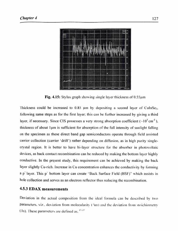
Chap/er 4 127
Fig. 4.15: Sty lus graph sho\\ ing single layer thickness of O.55p m
Thickness could be increased to 0 .85 ~lIn by depos it ing a second layer o f CulnSc~,
following same steps as fo r the first layer: this can be fUlther increoscd by giving a third
layer, if necessary . Since C IS possesses a vcry strong absorpt ion coeffic ient ( - 1 OS cm·1 ).
thickness of about I 'till is sufficient fo r absorpt ion of the full intensity of s \l111 igh l till ling
on Ihe specimen as these direct band gap semiconductors opcrate th rough tield ass isted
carrier collection (carrier 'drii1' ) rather depending on dill usion. as in hi gh purity sin gle
cryst<ll region. It is bener to have bi - Iayer slnu; lu rc fo r the absorllcr in photovo lta ic
dcvices, as back contact recombination can be reduced by makin g the bottom layer highly
conducti ve . In the pr~sent stUlJy. Ihis requi rement can he achieved by making Ihe back
laycr slightly Cu-rich. Increase in Cu concentration cllhallct.!s th t.! condu!; ti vily by for11lillg
a p- layer. Th is p ' bottom layer can create "Back Surface Fie ld (HSF)" \\ hich nss isls in
ho le co llection and serves as an electron rc llector thus reduc ing the rcco mbination.
4.5.3 EDAX measurements
Deviation in Ihe ,,!;Iual I.;omposition lI'om Ih~ ideal formula !;:J.n bt! (Ic:-;!; ribed by 1\\ 0
parameters. viz .. de\·ialion fi'olll l1l o l ccll la r il ~ 1 \111 1 :Hld the d..:vialioll fr,1m ~ !t'il.; h i\'!lIC lr~·
( t\ S ). rhese paralll l' h.:r ... :If!: ddincd as. 1; · 1'
Modified technique for deposition of CulnSel thin films using... 128
Cu !:J.m=--1
In
and
!:J.s = 2 [Se ] -1 [ClI] + 3[/n]
If t-.m>O and t-.s>O the sample will be p-type and if t-.m<O and !:J.s<0, the sample will be n
type.
Atomic concentration of the constituent elements was determined using EDAX, at
different points along the entire length of the sample. Samples CIS I 0 was spatially non
unifonn in composition. In CIS I 0, Cu was found to be agglomerated and hence the
composition was different at different points. Average composition is given in table4.5.
Also formation of CU2Se phase was identified from the XRD studies, probably due to the
increased concentration of Cu. Mass of Cu evaporated was greater for CIS 10 than CIS9.
But due to the spatial non-unifonnity in CISIO, EDAX analysis showed nearly the same
composition for both the samples. Typical values are given in table 4.5. With increase in
Cu concentration in the solution, the atomic concentration of Cu in the sample (as per the
EDAX results) was also increasing.
Cu-rich films should be dominated by antisite (CUIn) acceptor defects, yielding strongly
p-type layers. However, in all cases, auto-compensation may be expected at high intrinsic
defect levels in order to maintain overall valence neutrality. CUln antisite defects move a
Cu +1 atom onto a nominally In +3 site, resulting in a net charge of -2. This can be
compensated for by the creation of a Se vacancy (net change in charge of +2) with a
resulting decrease in Se concentration as the Cu concentration increases as observed.
C/Japter4 129
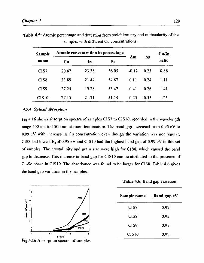
Table 4.5: Atomic percentage and deviation from stoichiometry and molecularity of the
samples with different Cu concentrations.
Sample Atomic concentration in percentage Cu/In ~m ~s
name Cu In Se ratio
C1S7 20.67 23.38 56.05 -0.12 0.23 0.88
CIS8 23.89 21.44 54.67 0.11 0.24 1.11
CIS9 27.25 19.28 53.47 0.41 0.26 1.41
CISIO 27.15 21.71 51.14 0.25 0.55 1.25
4.5.4 Optical absorption
Fig 4.16 shows absorption spectra of samples CIS7 to CIS 1 0, recorded in the wavelength
range 500 nm to 1500 nm at room temperature. The band gap increased from 0.95 eV to
0.99 eV with increase in Cu concentration even though the variation was not regular.
CIS8 had lowest Eg ofO.95 eV and CIS10 had the highest band gap of 0.99 eV in this set
of samples. The crystallinity and grain size were high for CIS8, which caused the band
gap to decrease. This increase in band gap for CIS 1 0 can be attributed to the presence of
CU2Se phase in CISIO. The absorbance was found to be larger for CIS8. Table 4.6 gives
the band gap variation in the samples.
-: 2
,," .. !
.. 10
'v(~')
Fig.4.t6 Absorption spectra of samples
Table 4.6: Band gap variation
Sample name
CIS7
CIS8
CIS9
ClSIO
Band gapeV
0.97
0.95
0.97
0.99
Modified technique for deposition of CulnSe2 thin films using... 130
I naIl the films. there existed a second absorption edge at energies near 1.1 e V as obtained
in the earlier case which could be attributed to the valence band splitting.
4.5.5 Electrical characterization
Table 4.7 gives the type of conductivity, photosensitivity and resistivity of the samples.
Type of conductivity was detennined to be p-type using hot probe method for all the
samples, except CIS7. Interestingly, CIS7 was the only In-rich sample in this series.
Excess 'In' might have created donor levels like Inj, Incu, Inse etc in CulnSe2 which
converted the conductivity type to n. For CIS7, the deviation from molecularity was <I
and hence the stoichiometry supported the n-type behaviour. For all other samples,
deviation from molecularity and stoichiometry was> I, and hence were showing p-t}'pe
conductivity.
Table 4.7: Type of conductivity and resistivity for the Cu varied samples
Sample name Type of carrier Photosensitivity Resistivity acm
CIS7 n -0.78 10.37
CIS8 P 0.17 76
CIS9 P 0.1 3
CISIO P -0.045 1.8x 10⁻³
For the n-type sample, the resistivity was 10.37 Ocm while resistivity of p-type samples
decreased with increase in Cu. Thus highly conductive (p -10-3 Ocm) as well as resistive
samples (p-76 Ocm) could be prepared using this method.
For device fabrication, usually slightly resistive samples (resistivity of the order of 10·
Ocm) are preferred, whereas the highly conductive films are used as the bottom layer of
the absorber near the electrode. This low resistivity CIS layer incorporated on the
contact-side lowers the series resistance R, of the device. Photosensitivity of the n-type
sample was negative and for the remaining samples its value was fractional. For the

Chapter 4 13 1
highly conductive sample. ClS IO. the photosensitivity aga in showed negative value. The
negat ive photosensitivity may be due to recomb ination of light generated minority
carriers with holes (electrons) at the top of the valence band (bottom of the conduction
band ).
4.5.6 Morphological analy<";<~
Morphological analys is carried out using AFM is shown in (Fig.4.17 (a}-(d» . The 3
dimensional AFM image showed that in CIS7 (i.e. the n-type sample). the grains were
agglomerated. These agglomerations might be due to the unreacted binary phases which
were not revealed in XRD analysis. These grains were separated indicating the reason for
low conductivity of this sample. There " as a distribut ion of grain size in the films. Grain
size ..-aried over a wide range. (from 61 nm to 202 nm).
(.)
( c) (d)
Fig. 4.17 Three dimensional AFM images of samples
(a l CIS7 (b) CIS8 (c) CIS9 (d ) CIS10
Modified technique for deposition of Cu/nSez thin films using... 132
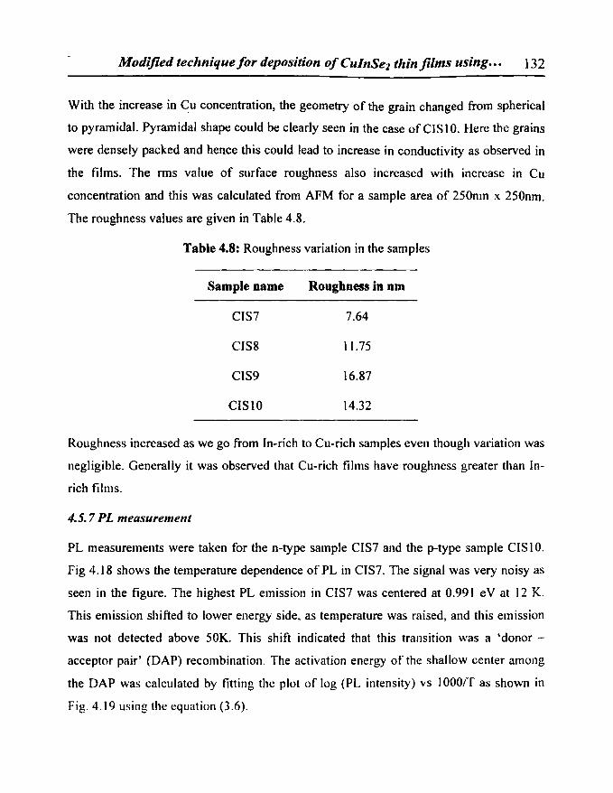
With the increase in ~u concentration, the geometry of the grain changed from spherical
to pyramidal. Pyramidal shape could be clearly seen in the case of CIS 1 O. Here the grains
were densely packed and hence this could lead to increase in conductivity as observed in
the films. The nns value of surface roughness also increased with increase in Cu
concentration and this was calculated from AFM for a sample area of 250nm x 250nm.
The roughness values are given in Table 4.8.
Table 4.8: Roughness variation in the samples
Sample name Roughness in om
CIS7 7.64
CIS8 11. 75
CIS9 16.87
CISI0 14.32
Roughness increased as we go from In~rich to ClI-rich samples even though variation was
negligible. Generally it was observed that Cu-rich films have roughness greater than In
rich films.
4.5.7 PL measurement
PL measurements were taken for the n~type sample CIS7 and the p-type sample CIS 1 O.
Fig 4.18 shows the temperature dependence of PL in CIS7. The signal was very noisy as
seen in the figure. The highest PL emission in CIS7 was centered at 0.991 eV at 12 K.
This emission shifted to lower energy side, as temperature was raised, and this emission
was not detected above 50K. This shift indicated that this transition was a 'donor -
acceptor pair' (OAP) recombination. The activation energy of the shallow center among
the OAP was calculated by fitting the plot of log (PL intensity) vs 1000/'f as shown in
Fig. 4.19 using the equation (3.6).
Chapter 4
i -I =! I .!.I
i ~
X5 :--soKI
0116 098 100 102 1.0.4 10$ 101 "0
Energy,.V)
Fig. 4.18: Temperature dependence of PL spectra of sample CIS7 (CulIn=O.88)
133
The activation energy was obtained to be 13 meV which agreed with the activation
energy of the In~II donor level. Neglecting the Coulomb term and using ED = 13 meVand
Eg = 1.042 eV in equation (3.5) EA was obtained as 38 meV which agreed with the
activation energy of the VCII acceptor level. Hence this emission could be assigned to the
In~" - VCII OAP recombination.
• experimental Filling
1000lT IK')
Fig. 4.19: Plot of 1000/T vs log (integrated PL intensity) of
CIS7 fitted using equation (4.2)
Modified technique for deposition of CulnSel thin films using... 134
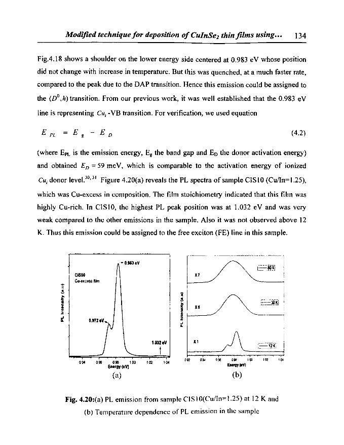
Fig.4.18 shows a shoulder on the lower energy side centered at 0.983 eV whose position
did not change with increase in temperature. But this was quenched, at a much faster rate,
compared to the peak due to the DAP transition. Hence this emission could be assigned to
the (DO ,h) transition. From our previous work, it was well established that the 0.983 eV
line is representing ell; -VB transition. For verification, we used equation
E PL (4.2)
(where EpL is the emission energy, Eg the band gap and Eo the donor activation energy)
and obtained ED = 59 meV, which is comparable to the activation energy of ionized
ell; donor level.30, J I Figure 4.20(a) reveals the PL spectra of sample CIS I 0 (CulIn= 1.25),
which was Cu-excess in composition. The film stoichiometry indicated that this film was
highly Cu-rich. In CISI0, the highest PL peak position was at 1.032 eV and was very
weak compared to the other emissions in the sample. Also it was not observed above 12
K. Thus this emission could be assigned to the free exciton (FE) line in this sample.
C\S!O CU-lIlCess liJm
U32tV
! 09« 0.96 09& 100 ICl 104
Energy(eV)
(a)
I~,,,,,,,,,,,, , l"'~-_. ~ ----~--",;l.
X7 ~
; I I j--lO!j
i
XI
O~ O~ O~ O~ 1~ 1~ 1~
£Mf9Y1'V)
(b)
Fig. 4.20:(a) PL emission from sample CIS I O(Cu/ln=1.2S) at 12 K and
(b) Temperature dependence of PL emission in the sample
Chapter 4 135
Multiple Fit for spectrum at 20 K Mulllple Fit for spedJum at 80 K
.... 0.95 O.fl6 0.97 0.98 099 1 00 , 01 0904 095 0915 097 0.88 O.W 1 co 1.01 1.02 103
Energy (eY) ErmgyleV)
(a) (b)
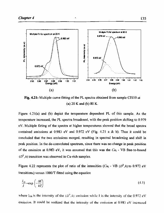
Fig. 4.21: Multiple curve fitting of the PL spectra obtained from sample CISIO at
(a) 20 K and (b) 80 K.
Figure 4.21 (a) and (b) depict the temperature dependent PL of this sample. As the
temperature increased, the PL spectra broadened, with the peak position shifting to 0.979
eV. Multiple fitting of the spectra at higher temperatures showed that the broad spectra
contained emissions at 0.983 eV and 0.972 eV (Fig. 4.21 a & b). Thus it could be
concluded that the two emissions merged, resulting in spectral broadening and shift in
peak position. In the de-convoluted spectrum, since there was no change in peak position
of the emission at 0.981 eV, it was assumed that this was the CUi - VB free-to-bound
(Do,") transition was observed in Cu-rich samples.
Figure 4.22 represents the plot of ratio of the intensities (CUi - VB (Do,h) to 0.972 eV
transitions) versus I ooorr fitted using the equation
(4.5)
where IOh is the intensity of the (Dil,1!) emission while I is the intensity of the 0.972 eV
emission. It could be realized that the intensity of the emission at 0.983 eV increased
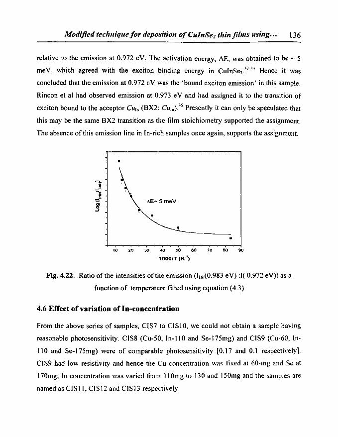
Modified technique/or deposition o/CulnSe2 thinjilms using... 136
relative to the emission at 0.972 eV. The activation energy, ~E, was obtained to be - 5
meV, which agreed with the exciton binding energy in CuInSe2.32.34 Hence it was
concluded that the emission at 0.972 eV was the 'bound exciton emission' in this sample.
Rincon et al had observed emission at 0.973 eV and had assigned it to the transition of
exciton bound to the acceptor CUln (BX2: CUln).3S Presently it can only be speculated that
this may be the same BX2 transition as the film stoichiometry supported the assignment.
The absence of this emission line in In-rich samples once again, supports the assignment.
I
•
.\E- 5 meV
• 10 20 30 <10 50 60 70 80 90
1000/T (K")
Fig. 4.22: .Ratio of the intensities of the emission (lDh(0.983 eV) :I( 0.972 eV» as a
function of temperature fitted using equation (4.3)
4.6 Effect of variation of In-concentration
From the above series of samples, CIS7 to CIS 1 0, we could not obtain a sample having
reasonable photosensitivity. CIS8 (Cu-50, In-l1 0 and Se-175mg) and CIS9 (Cu-60, In-
110 and Se-175mg) were of comparable photosensitivity [0.17 and 0.1 respectively].
CIS9 had low resistivity and hence the eu concentration was fixed at 60-rng and Se at
170mg: In concentration was varied from 11 Omg to 130 and 150mg and the samples are
named as CISII, CISI2 and CISIJ respectively.
Chapter 4 137
4.6.1 Structural Characterization
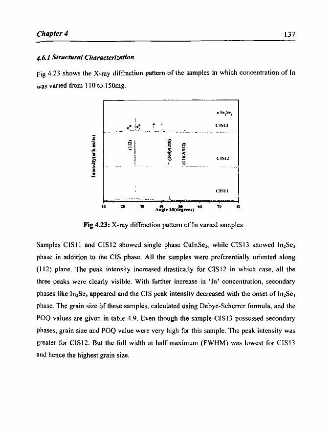
Fig 4.23 shows the X-ray diffraction pattern of the samples in which concentration of In
was varied from 110 to 150mg.
CISI3
CISll
ClSII
10 711
Fig 4.23: X-ray diffraction pattern of In varied samples
Samples CIS 11 and CIS 12 showed single phase CuInSe2, while CIS 13 showed In2Se3
phase in addition to the CIS phase. All the samples were preferentially oriented along
(112) plane. The peak intensity increased drastically for CISI2 in which case, all the
three peaks were clearly visible. With further increase in 'In' concentration, secondary
phases like In2Se3 appeared and the CIS peak intensity decreased with the onset of In2Se)
phase. The grain size Of these samples, calculated using Debye-Scherrer fonnula, and the
POQ values are given in table 4.9. Even though the sample CIS 13 possessed secondary
phases, grain size and POQ value were very high for this sample. The peak intensity was
greater for CIS 12. But the full width at half maximum (FWHM) was lowest for CIS 13
and hence the highest grain size.
Modified technique for deposition of CulnSel thin films using... 138
Table 4.9 Variation in grain size and POQ values
Sample name POQ
4.6.2 EDAX measurements
CIS11
CISl2
CIS13
3
4
5
Grain Size
nm
35
42
65
Table 4.10: Atomic concentration and deviation in molecularity and stoichiometry
Sample
name
CIS 11
CIS 12
Atomic concentration in percentage
Cu
27.25
17.12
In
19.28
31.48
Se
53.47
51.39
~m
0.41
-0.46
0.26
-0.08
Table 4.10 clearly indicates that, C IS 11 was Cu-rich and CIS 12 was highly In-rich. The
table also gives the deviation from molecularity and stoichiometry. For the ell-rich
sample, both these values are positive and for the In-rich sample the values are negative.
4.6.3 Optical Absorption
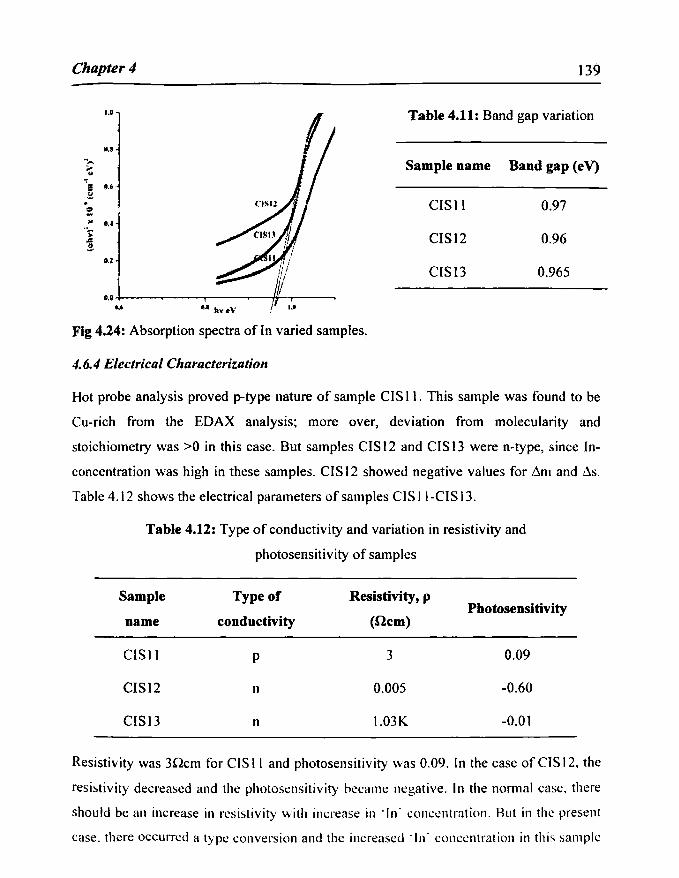
Absorption spectra were recorded in the range 1500 to 500nm. Fig 4.24 shows the
absorption spectrum of the In-varied samples. From the table 4.11, it was found that band
gap varied slightly.
Chapter 4 139
I.' Table 4.11: Band gap variation
Sample name Band gap (eV)
CISII 0.97
CISI2 0.96
CIS13 0.965
O.O+--~----r------!~"---~ ... Fig 4.24: Absorption spectra of In varied samples.
4.6.4 Electrical Characterizatioll
Hot probe analysis proved p-type nature of sample CIS 11. This sample was found to be
Cu-rich from the EDAX analysis; more over, deviation from molecuIarity and
stoichiometry was >0 in this case. But samples CIS 12 and CIS 13 were n-type, since In
concentration was high in these samples. CIS 12 showed negative values for ~m and ~s.
Table 4.12 shows the electrical parameters of samples CIS 1 I-CIS 13.
Table 4.12: Type of conductivity and variation in resistivity and
photosensitivity of samples
Sample Type of Resistivity, p Photosensitivity
name conductivity (ncm)
CISI1 p 3 0.09
CIS12 n 0.005 -0.60
CIS13 n 1.03K -0.01
Resistivity was 3ncm for CIS 1I and photosensitivity was 0.09. In the case of CIS 12, the
resistivity decreased and the photosensitivity became negative. In the normal case, there
should be an increase in resistivity with increase in 'In' concentration. But in the present
case. there occurred Cl type conversion and the increased 'In' concentration in this sample
Modified technique for deposition of CulnSe2 thin films using... 140
gave way to decreased resistivity. With further increase in 'In' concentration, [Le. for
CIS 13], the resistivity again increased. This increase can be attributed to the presence of
binary phase in this sample.
4.6.5 Discussion
'In' concentration was varied in the samples. The samples CIS12 and CISJ3 were n-type
while CISII was p-type. Also, on increasing mass of 'In' evaporated to 150 mg. there
occurred In2Se3 phase in addition to the CIS phase. Hence it was concluded that 'In'
concentration of 110 or below should be used in the present work. However, this n-type
layer can be made use of for the fabrication of homo junction solar cells.
4.7 Minute variations of Cu and In concentrations
From the characterizations carried out above, only CISS (Se-170, In-IIO and Cu-50)
exhibited reasonable photosensitivity. Minute variations in Cu and In concentrations were
made to achieve better photosensitivity in the samples. However concentration of Se was
fixed in all the cases. Samples were prepared with masses In-112mg and Cu-
5Img(CISI4), In-I IOmg and Cu-46mg(CISI5), In-112 and Cu-50(CISI6), In-114 and
Cu50mg(CIS 17), In-liS and Cu-50mg(CIS IS). Table 4.13 shows the photosensitivity
and resistivity of these samples.
Table 4.13 Electrical parameters of the samples CIS 14 to CIS IS
Sample Resistivity Photosensitivity
Type of
name nem Conductivity
CIS14 0.019 0.02 p
CISI5 0.114 0.02 p
CISI6 0.011 -0.02 P
CISI7 2.6 -0.07 P
CISI8 9.3 0.1 n
Chapter 4 Ut
from the table, it is clear that the photosensitivity of the p-type samples was very low and
conductivity changed to n type, when In-concentration was increased to 118mg.
4.8 Optimization for solar cell fabrication
In order to get ideal samples for device fabrication, further variation in stoichiometry was
carried out. Concentration of Se was fixed at 175 mg and that of Indium at 100 mg and
mass of Cu was varied from 20 to 50 mg in steps of 10 mg so that Culln ratio was 2.37,
1.48, 1.13, and 0.98 respectively, as obtained from EDAX. The samples were named as
CISO.2, CISO.3, CISO.4 and CISO.5. These samples were fully characterized to find the
suitability for device fabrication.
4.8.1 Structural Characterization
Structural characterization was perfonned using X-ray diffraction and Raman analysis.
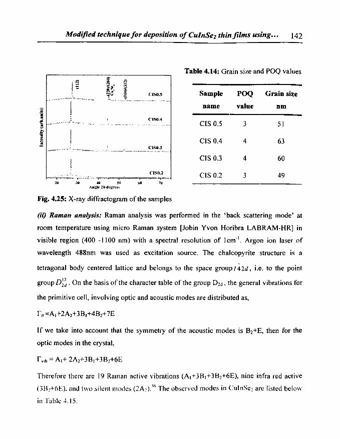
(i) XRD: Fig 4.25 shows the XRD pattern of the samples. Peaks were observed in the
(112), (220)/(204) and (116)/(312) planes with preferential orientation along (112)
dir~ction as observed earlier. As Cu concentration increased, the crystallinity also
increased. Cu-rich films are generally more crystalline than In-rich films. In the case of
Cu rich films, there occurs a liquid phase of CuxSe which enhances the grain growth.
Crystallinity was better for CISO.4 and decreased with further increase in Cu
concentration. In the case of CISO.5, for which Cu concentration was the maximum,
secondary phase of CU3Se2 was observed. However grain size and POQ value were high
for CISO.4 and the values are listed in the table 4.14
The XRD profile contained only the common peaks corresponding to sphalerite and
chalcopyrite structures as obtained earlier. To confirm the structure of the CulnSe2 films,
Raman analysis was carried out on these samples.
Modified technique for deposition of CulnSel thin films using... 142
10
i !:: ~,,= ~ ~~; CfSO.~
' ..... _. -"'-'--~-'-. ,~""".~ .. "
CISO."
nSII.2
.\8 -HI ~o 7U .\n~l~ "!o d,~~rt'~~
Fig. 4.25: X-ray diffractogram of the samples
Table 4.14: Grain size and POQ values
Sample POQ Grain size
name value nm
CIS 0.5 3 51
CIS 0.4 4 63
CIS 0.3 4 60
CIS 0.2 3 49
(U) Raman analysis: Raman analysis was performed in the 'back scattering mode' at
room temperature using micro Raman system [Jobin Yvon Horibra LABRAM-HR] in
visible region (400 -1100 nm) with a spectral resolution of I cm' I. Argon ion laser of
wavelength 488nm was used as excitation source. The chaIcopyrite structure is a
tetragonal body centered lattice and belongs to the space group 142d, i.e. to the point
group D~~ . On the basis of the character table of the group D2d , the general vibrations for
the primitive cell, involving optic and acoustic modes are distributed as,
If we take into account that the symmetry of the acoustic modes is B2+E, then for the
optic modes in the crystal,
Therefore there are 19 Raman active vibrations (A1+3B 1+3B2+6E), nine infra red active
(3B2+6E). and two silent modes (2A 2 ).11> The observcU modes ill CulnSc2 are listed belo ....
ill Table .. L 15.
Chapter 4
Table 4.15: The different vibrational modes observed in CulnSe2
Frequency(cm-1)
Approximate relative Assignment
strength (%)
259 15 E
231 8 B2,E
215 22 B2,E
206 10 E
174 100 AI
124 20 BI ,
76 35 BI
61 30 B2
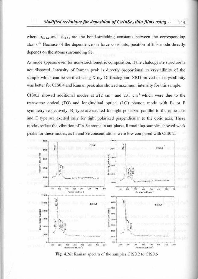
Figure 4.26 shows the Raman spectra of the samples. All the samples showed a
prominent peak at 174 cm-I, which is the characteristic peak of chalcopyrite structure.
This peak corresponds to Al mode in which Se atoms vibrate in the x-y plane with Cu
and In atoms at rest. Hence frequency of this mode is associated with Se mass and the
cations-Se bond stretching forces, describing the interaction between nearest neighbors.
The frequency of the Al mode is given by
( k )11 Z
V = -M Se
where k is the force constant and Msc, mass of Se atom.36 Dependence ofv on these force
constants can be expressed as
1 2(a,... ~ + at s') Ir (AI) = L 11-.'" ll-d
Ms,.
Modified technique for deposition ofCuhiSe, thin films using;i, 144
where Clcu-Se and Uln- Se are the bond-stretching constants between the corresponding
atoms." Because of the dependence on force constants, position of this mode directly
depends on the atoms surrounding Se.
AI mode appears even for non-stoichiometric composition, if the chalcopyrite structure is
not distorted. Intensity of Raman peak is directly proportional to crystallinity of the
sample which can be verified using X-ray Diffractogram. XRD proved that crystallinity
was better for CISO.4 and Raman peak also showed maximum intensity for this sample.
CISO.2 showed additional modes at 212 cm-I and 231 cm" which were due to the
transverse optical (TO) and longitudinal optical (La) phonon mode with B2 or E
symmetry respectively. 8 2 type are excited for light polarized parallel to the optic axis
and E type are excited only for light polarized perpendicular to the optic axis. These
modes reflect the vibration of In-Se atoms in anti phase. Remaining samples showed weak
peaks for these modes, as In and Se concentrations were low compared with CISO.2.
, j I
JOOl I+h) ~on
I-bmall 'l.hi(fjem·')
CIStU
I600
3~OO l
,'~ J~';
i'''....! .:::
.=. 1$011
."'..JIW, ~no .~i"' -.100 ff~l M~) ":'if(l
Raman ~b ihf(~m -I)
LW{)O, ············ ··················· ········· ········· ,.~(IO ,.---------------,
101".10 C1S0.~ C ISO.5
f l' l' j
Il~ l !I Mt .~I M . ~lJn 10,;(1 NKl ':Illt t
Raman shih( CiO'!)
I , I I,l Ofl UH) .otIlO M II
H:lm an "hinl,-m-Ill ll ll
i.Ii
:f 8000=~.:~ hUOt)
i ''''"11
2""·1e .L.,.--r-~.-----,r----r~--,--r-o--.
lHo
Fig. 4.26: Raman spectra of the samples CISO.2 to CISO.5
Chapter 4 145
With the increase in Cu concentration (CISOo4), B2 mode showed a slight shift to 226 cm
I and this may be due to vacancy of Indium or stress in the sample_ For CISO.3 and
CISO.4, an additional mode at 260cm-1 could be seen. This peak is assumed to be the
highest frequency mode in CulnSe2' This mode is reported to be due to Cu,Se binary
phase by many authors.38,39 In the present case, this peak disappeared for the Cu-rich
sample CISO.S which contained CU3Se2 phase. Hence it was concluded that this peak was
not due to any CuxSe phase and could be attributed to B2+E mode. Intensity of the AI
mode was better for CISOo4 which also shows that it is the most ordered stnlcture.
Raman spectra 0 f Cl SO A showed a shoulder at ISO cm -I. wh ich corresponds to the
highest frequency BI mode. This peak showed a slight decrease from the original value of
160cm- l_ This may be due to stress in the sample_ The BI mode corresponds to the
frequency of vibration of Cu and In atoms in antiphase. In this case, the polarizability
changes during the vibration due to the stretching of the Cu-In bond are partially
compensated by the compression of the In-Se bond and hence this mode is very weak_
Frequency of this mode is given bi6
k(M +M )112 Y = Cu In
( )11'
M CI/NIIII -
Mode at 150cm-1 is also reported to be due to In-Se compounds. As the composition was
Cu-rich, in the present case, this possibility could be avoided.
From the Raman analysis of the samples, we could confirm that the structure was
chalcopyrite which was the most favorable stnlcture for solar cell fabrication. The
compositional variation was reflected in the Raman spectrum also. Intensity of the AI
mode was directly linked with the crystallinity. Hence from the FWHM of the Raman
peak, one could have an idea about the crystallinity of the films.
Modified technique for deposition of Cull,Sez thin films using... 146
4.8.2 Compositional analysis
(i) EDAX measurements: Elemental concentrations were determined using EDAX and
depth-wise analysis of the sample was carried out using XPS measurements. The atomic
concentrations in percentage are given in the table 4.16. CISO.5 has Cu concentration of
32.79% for which CU3Se2 phase was observed. From the table, it is clear that on
decreasing Cu concentration, In and Se concentrations increase correspondingly. On
reaching CISO.3, the concentration of In remained almost steady and hence for CISO.2,
Se concentration increase sharply to 60.04%.
Table 4.16 Atomic concentration and deviation from stoichiometry and molecularity
Sample Atomic concentration in percentage ~m ~s
name Cu In Se
CIS 0.5 32.79 13.82 53.39 1.37 0.44
CIS 0.4 27.04 18.29 54.67 0.48 0.33
CIS 0.3 22.84 20.19 56.97 0.13 0.37
CIS 0.2 19.75 20.21 60.04 -0.022 0.49
The deviation from molecularity (~m) and stoichiometry (~s) of the samples were also
listed in the table. CISO.2 showed a slight negative value for ~m.
(ii) XPS analysis: XPS analyses were performed for the samples CISO.2 and CISO.4.
Depth-wise XPS analysis was done, employing argon ion sputtering. Figures 4.27-4.28
show the XPS profile of CISO.2. The shift in the binding energy (BE) of In and Se at the
surface layers could clearly be seen. On comparing the binding energies it was observed
that In1SeJ was formcd at the surface. After two layers, the formation of CuInSe2 was
evident from the binding energy shift. In the case of CulnSe2, binding energies of Cu, In
and Se are Se-54.6 eV and In-444.7 eV respectively. From EDAX, the sample \vas
identified as highly Se-rich. This may be the reason fix thc flmnation of In2ScJ. However,
(i·om the XRD analysis. we could get only the CulnSe2 phase.
Chapter 4 147
';;- 'A .. " 5 .~ ~
'" ~ '" ...l .-! u t >' t.-
930 9·10 950 91>0 970 440 445 450 455 460 BINDING ENERGY (cV) BINDING ENERGY (cV)
(a) (b)
Fig. 4.27: XPS depth profile of (a) Cu in CISO.2 (b) In in CISO.2
Figure 4.27(a) shows the depth-wise analysis of Cu concentration. It can be seen that, Cu
was absent in the surface layers of the sample. The peak intensity was high after two
cycles of etching. Binding energies of 932 and 952.2eV were corresponding to CU2Pl12
and CU2P3/2 states in CulnSe2 respectively.
The depth-wise analysis of In (Fig. 4.27(b» shows a shift in binding energy for the two
layers at the surface. The binding energies of 445.5 and 453.5eV were corresponding to
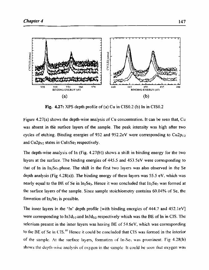
that of In in In2Se3 phase. The shift in the first two layers was also observed in the Se
depth analysis (Fig 4.28(a». The binding energy of these layers was 55.5 eV, which was
nearly equal to the BE of Se in InzSe3' Hence it was concluded that In2Se3 was fonned at
the surface layers or-the sample. Since sample stoichiometry contains 60.04% of Se, the
formation of In1Se3 is possible.
The inner layers in the 'In' depth profile [with binding energies of 444.7 and 4S2.1eV]
were corresponding to In3d3l2 and In3ds/2 respectively which was the BE of In in CIS. The
selenium present in the inner layers was having BE of 54.6eV, which was corresponding
to the BE of Se in eIS. 1n Hence it could be concluded that ClS was formed in the interior
of the sample. At the surface layers, fOl1l1ation of In,se; was prominent. Fig 4.28(b)
shows the depth-\vise analysis or OXygL'J1 in the sal11pk. It could be seen that oxygen was
Modified technique for deposition of CulnSel thin films using... 148
absent in the bulk of the sample. Oxygen occurred as a surface contamination at the top
layer of the sample.
55 60 65 70 525 510 535 540 545 BINDING FNERGY(eY) BINDING ENERGY (cV)
(a) (b)
Fig 4.28: XPS depth profile of (a) Se in CISO.2 (b) of 0 in CI~0.2
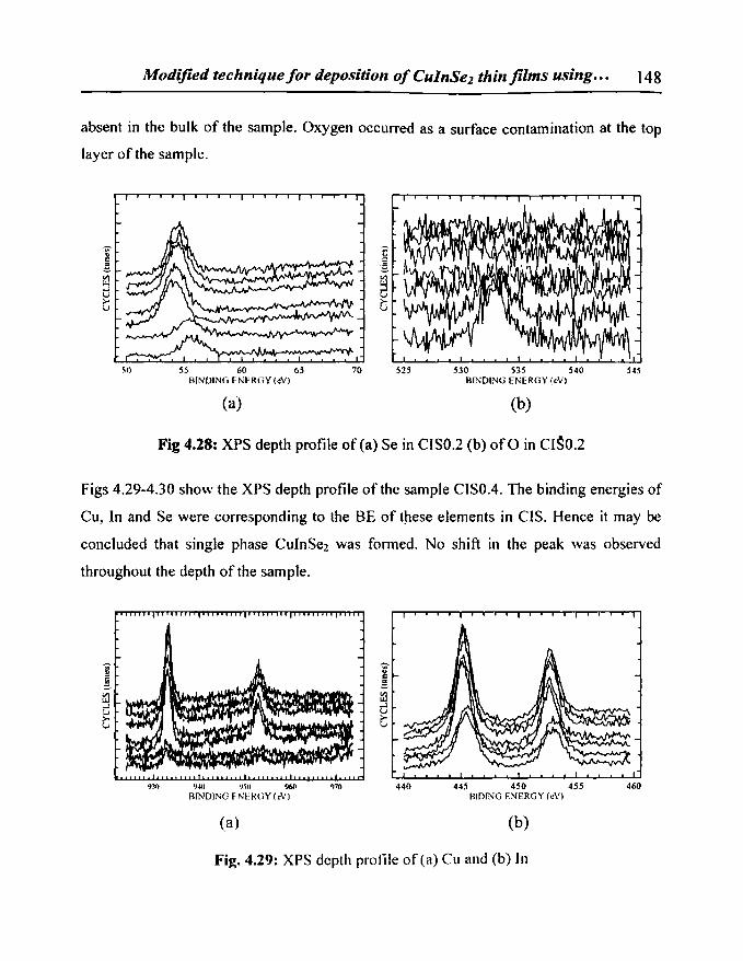
Figs 4.29-4.30 show the XPS depth profile of the sample CISOA. The binding energies of
Cu, In and Se were corresponding to the BE of tpese elements in CIS. Hence it may be
concluded that single phase CuInSe2 was fonned. No shift in the peak was observed
throughout the depth of the sample.
9)0 1)40 9~O 960 440 445 450 455 460 BINDlNG Fi'iERGY«V) BIf)(NG ENERGY (cV)
(a) (b)
Fig. 4.29: XPS depth profile of (a) ClI and (b) In
Chapter 4 149
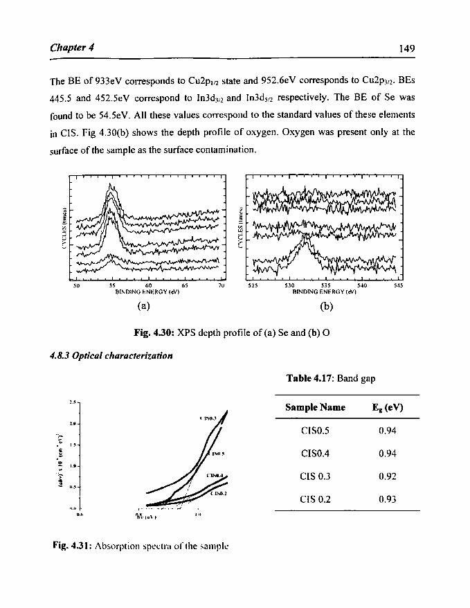
The BE of 933eV corresponds to Cu2Pln state and 9S2.6eV corresponds to CU2P3/2' BEs
445.5 and 4S2.5eV correspond to In3d3i2 and In3dsI2 respectively. The BE of Se was
found to be S4.SeV. All these values correspond to the standard values of these elements
in CIS. Fig 4.30(b) shows the depth profile of oxygen. Oxygen was present only at the
surface of the sample as the sUlface contamination.
50 55 60 65 70 525 530 535 540 5·15 BINDING ENERGY (cV) BINDING ENERGY (e\')
(a) (b)
Fig. 4.30: XPS depth profile of (a) Se and (b) 0
4.8.3 Optical characterization
Table 4.17: Band gap
!.~
Sample Name
1 .•
.~ CISO.S 0.94
.. I.~
~ CISO.4 0.94 ~ I.D .. . ~
i I •. ~
CIS 0.3 0.92
...• 1 CIS 0.2 0.93 •.. 'tt~·I.\ I
I.u
Fig. 4.31: Absorption spectra of the sample
Modified technique for depos'ition of CulnSez thin films using... 150
Optical absorption of the sample CISO.2-CIS 0.5was measured in the range from SOOnm
to IS00nm. [Fig 4.31 ].There was no significant variation in the band gap of the samples.
However, there was a visible change in the value of the absorbance of these samples.
CISO.3 showed higher absorbance and CISO.2, the least. The Eg values are listed in table
4.17
4.8.4 Electrical characterization
All the samples showed p-type conductivity. Even though there was deviation from
molecularity [tlm<O] for CISO.2, the sample showed p-type conductivity. This may be
due to the increased Se concentration. Resistivity and photosensitivity were high for
CISO.2. The photosensitivity of the sample gradually changed from positive to negative
on increasing the Cu concentration. The high resistivity for CISO.2 may be due to the
presence ofIn2Se3 phase as observed in XPS analysis.
Table 4.18: Resistivity and photosensitivity variation in the samples
Sample p(ficm) Photosensitivity
name
CIS 0.5 3.2 X 10.3 Negative
CIS 0.4 SX 10.2 Negative
CIS 0.3 8X 10.2 0.001
CIS 0.2 8X 10² 4
For device fabrication, both high and low resistivity CIS are needed as Copper cones will
be formed at the junction, when low resistivity CIS is used throughout. This will provide
shunting paths. destroying junction properties.
Chapter 4 151
4.8.5 Discussion
Highly resistive and highly conductive CuInSe2 samples could be prepared using the
technique developed in the present work. CISO.2 was the most photosensitive sample.
However, this sample contained secondary phase of In2Se3 which made it unsuitable for
solar cell fabrication. CISO.3 can be used as the conductive bottom layer of the solar cell
because of its low resistivity. For device fabrication, a slightly resistive layer should be
used at the junction. To find this Se concentration was varied slightly.
4.9 Variation of Se concentration
Concentration of Se was varied slightly, keeping the concentrations of Cu and In fixed at
20 and 100 mg respectively. 165 and 185 mg of Se were evaporated for further
optimization. These samples were named as CIS 165, CIS 175 and CIS 185 with masses of
Se as 165, 175 and 185 mg respectively.
4.9.1 Structural Characterization
XRD analysis of CIS J 65, CIS 175 and CIS 185proved the existence of single phase CIS
preferentially oriented along (112) plane [Fig.4.32]. (220)/(204) and (312)/(116) planes
were also identified from XRD, as in the earlier case.
I CISI85 , ... ,-~'-----".-'.--"-,-------"; " of ~
N i =-i ... :r .., c s;: ...
:! C1S175 t!
nS16$
-~~-----""----.-------' la lit 70
Fig. 4.32: X-ray diffractogram of the Se varied samples

Modified technique for deposition of CulnSe2 thin films using... 152
Among these, crystallinity was high for Se concentration of 165mg and it decreased
sharply for CIS 185. The grain sizes together with the quality factors are given in the
Table 4.19. Maximum grain size and POQ were obtained for Se concentration of 165mg
and it decreases with increase in Se concentration.
Table 4.19 Grain size and POQ variation
Sample name
CIS165
CISI75
CISl85
4.9.2 EDAX measurements
POQ
4.6
4.5
3.8
Grain size (nm)
54
51
45
Atomic concentration was determined using EDAX analysis. Table 4.20 gives the atomic
concentration and deviation from molecularity and stoichiometry. CIS 165 was In-rich,
which had a suitable value for device fabrication. In CuInSe2 based solar cells, the layer
used near the junction ha~ In concentration -26%. Hence the layer of CIS 165 can be used
in solar cells. With the increase in mass of Se, the atomic percentage was also found to
increase. For CIS 175, the Se concentration reached 60.04%.
Table 4.20 Atomic concentration and deviation from molecularity and stoichiometry
Sample Atomic concentration in percentage ~m
name Co In Se
CIS165 21.55 26.21 52.24 -0.18 0.043
CISI75 19.75 20.21 60.04 -0.022 0.5
CISI85 18.62 27.13 54.25 -0.34 0.085
On increasing Se concentration to 1 85mg, the EDAX results did not show the same trend.
A n:ductioll in Se concentration was observed in this case. Rc-evaporation of Se may be

Chapter 4 153
the reason for this reduced Se concentration. In all the cases, deviation from molecularity
showed a negative value, since Cu concentration was less than the In concentration in
these samples. Still, ~s was greater than zero for all the samples.
4.9.3 Optical characterization
The band gap of the film showed a slight variation with change in Se concentration. The
band gap was found to be least for the Se-rich sample (0.93eV). [Table 4.21 ]
Table 4.21: Band gap variation with Se concentration
Sample name Band gap eV
CIS 165 0.95
CIS 175 0.93
CIS185 0.95
The rest of the two samples showed same band gap of - 0.95 eV. In CISI65 and CISI85,
In concentration was also high, which leads to the increase in band gap of the films.
Figure 4.33 and Fig. 4.34 shows the absorption spectra of the Se varied samples. The
absorbance was high for CIS 185.
o.~
tI.O+---....---.....--:=--,....-,'-+-.----~
1.0
Fig. 4.33 Absorption spectra of C I S 175 and Cl S 185
Modified technique for deposition of Cu/t,Se2 thin films using... 154
1.411
'_15
;... ~ us '11
~ Ut
! -c. D.I!' > 1 ...., 0.18
'"+-----T-----r-----~~~----~ U U
bye\'
Fig. 4.34 Absorption spectra of CIS 165
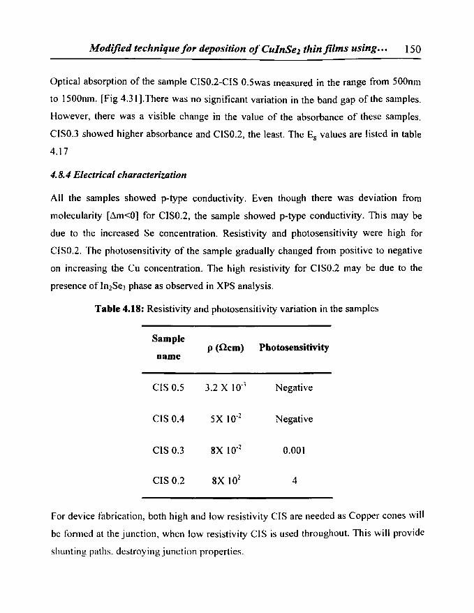
4.9.4 Electrical characterization
Hot probe measurement proved that all the samples were p-type. Electrical resistivity and
photosensitivity are depicted in Table 4.22. With increase in Se concentration, the
resistivity shows a decrease. Increase in Se will increase acceptor concentration making
the conductivity also high. The photosensitivity increased to 7.7, on decreasing the Se
concentration.
Table 4.22 Resistivity and photosensitivity variation in the samples
Sample name Resistivity p (Gem) Photosensitivity
CIS165 7916 7.7
CISI75 SOO 3.7
CISIS5 720 2.S
From the above analysis, it could be concluded that CIS 165 possessed suitable resistivity
and photosensitivity for device fabrication and hence this layer could be lIsed near the
junction. The sample CIS 165 was prepared repeatedly to ensure consistency in the
prope11ies.
CI.apter4 155
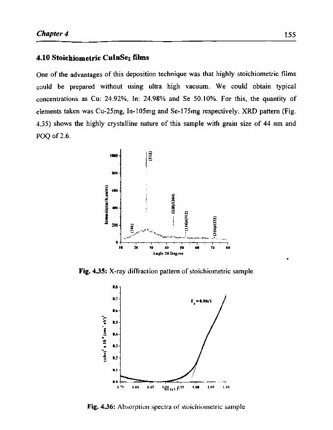
4.10 Stoichiometric CuInSez rtIms
One of the advantages of this deposition technique was that highly stoichiometric films
could be prepared without using ultra high vacuum. We could obtain typical
concentrations as Cu: 24.92%, In: 24.98% and Se 50.10%. For this, the quantity of
elements taken was Cu-25mg, In-I05mg and Se-175mg respectively. XRD pattern (Fig.
4.35) shows the highly crystalline nature of this sample with grain size of 44 nm and
POQ of2.6.
1-
'+.---r~-r~-.~-r~~~~~~ n ~ ~ ~ ~ ~ ~ h
..\"111. 211 D.,.r ••
Fig. 4.35: X-ray diffraction pattern of stoichiometric sample
0.8
D.7 f. ,. '.98<:V • 0 ••
. ~ U ..
~
E ~ u . ! .. 8.J
-; .c: fU ~
0.1
Fig. 4.36: Absorption spectra of stoichiometric sample
Modified technique/or deposition o/CulnSel thin films using... 156
Band gap (Fig 4.36) of this ideal sample was 0.98 eV and thickness was 0.58 J.1m. The
sample was p-type in nature and had a resistivity of 2 Qcm. The sample exhibited very
poor photosensitivity of 0.024, probably due to low resistivity of the sample.
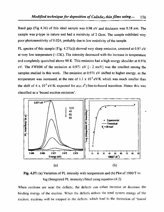
PL spectra of this sample (Fig. 4.37(a» showed very sharp emission, centered at 0.97 eV
at very low temperature (-12K). The intensity decreased with the increase in temperature
and completely quenched above 90 K. This emission had a high energy shoulder at 0.976
eV. The FWHM of the emission at 0.971 eV [~ 2 meV] was the smallest among the
samples studied in this work. The emission at 0.971 eV shifted to higher energy, as the
temperature was increased, at the rate of 1.1 x 10,5 e V IK which was much smaller than
the shift of 4 x 10,5 eV/K expected for a(e.Ao) free-ta-bound transition. Hence this was
classified as a 'bound exciton emission'.
• 12 K • 40 f S 60 80 J • i - • Experimental
~ r. - Theoretical • I c E =20meV
~ .
.J I (L
~ ..J
•
0.966 0.969 0972 0975 0978 10 20 30 40 50 eo 70 80 90
Energy (eVI 10001T(K')
(a) (b)
Fig. 4.37: (a) Variation ofPL intensity with temperature and (b) Plot of 1000rr vs
log (Integrated PL intensity) fitted using equation (4.2)
0
When excitons are near the defects. the defects can either increase or decrease the
binding energy of the exciton. When the defects reduce the total system energy of the
exciton. excitons will be trapped in the defects. which lead to the formation of 'bound

Chapter 4 157
excitons'. This gives rise to PL emission at lower energy than that of free excitons. TIlis
could be the reason to the absence of FE line was not observed in this sample. Bound
exciton emission lines exhibit narrower line-widths than free exciton emissions due to
increased localization. This supported our observation as to why the emission at 0.971 eV
exhibited very low FWHM. Since most semiconducting materials contain significant
amount of impurities and/or defects which can trap excitons, the identification of the
bound exciton states provides an important characterization of impurities, which control
the electra-optic properties of semiconductors. Neutral and ionized donors and acceptors
can trap excitons and form bound excitons.
The bound exciton emission from the sample was quenched above 80 K. In order to
calculate the PL quenching energy, a plot between logarithmic value of integrated PL
intensity versus 1000rr was fitted (Fig. 4.37(b» using the equation (4.2). The activation
energy (6E) of the impurity was obtained to be 20 meV. TIlis was in good agreement
with the reported activation energy of the doubly ionized In~,: donor level.42. 43 As
temperature was raised, the localization decreased due to the thermal ionization of the
defect center. This caused the bound exciton to become free, resulting in increase of
FWHM and PL peak energy. Thus it could be concluded that this was the 11(,: donor
bound exciton (BX:D2 (Illcu» emission in this sample.
4.11 DoubJ.e layer CulnSel
As the thickness of single layer was nearly 0.55 ~un, a double layer CIS was prepared
for cell fabrication. For this, a highly conductive bottom layer and highly resistive top
layer were selected. From the above optimizations, CIS 0.3 with a resistivity of 0.080cm
was ideal for the bottom layer and CIS 165 with a resistivity of 7916 Qcm was ideal as the
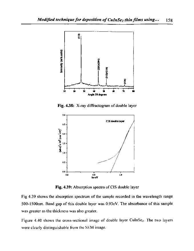
top layer. The thickness of this double layer was 0.9 J,l.ITI. X-ray diffractogram (Fig. 4.38)
proved the existence of single phase CulnSe1' Grain size was calculated to be 52 nm.
Modified technique/or deposition o/CulnSe2 thin films using... 158
,:r-e
3 § .cS ~ ~
f ~ B 'it ...
.5i i ... G
•
Fig. 4.38: X-ray diffractogram of double layer
3.D,-----------------,
.~
)U ", ~ I.!
1 I.D
D.!
Cls double layer
0.0 +---.....---~--.........,..-___,r__---.
u 0.' hveV
1.0
Fig. 4.39: Absorption spectra of CIS double layer
Fig 4.39 shows the absorption spectrum of the sample recorded in the wavelength range
SOO-ISOOnm. Band gap of this double layer was O.93eV. The absorbance of this sample
was greater as the thickness was also greater.
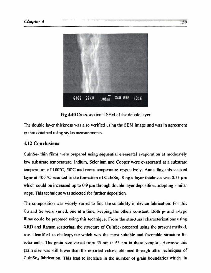
Figure 4.40 shows the cross-sectional image of double layer CulnSe2' The two layers
were clearly distinguishable from the SEM image.
Chapter 4 159
Fig 4.40 Cross-sectional SEM of the double layer
The double layer thickness was also verified using the SEM image and was in agreement
to that obtained using stylus measurements.
4.12 Conclusions
CulnSe2 thin films were prepared using sequential elemental evaporation at moderately
low substrate temperature. Indium. Selenium and Copper were evaporated at a substrate
temperature of 10O"C. 50"C and room temperature respectively. Annealing this stacked
layer at 400 "C resulted in the fonnation of CulnSez. Single layer thickness was 0.55 ~m
which could be increased up to 0.9 J.Utl through double layer deposition, adopting simi lar
steps. This technique was selected for further deposition.
The composition was widely varied to find the suitability in device fabrication. For this
Cu and Se were varied, one at a time, keeping the others constant. Both p- and n·type
films could be prepared using this technique. From the structural characterizations using
XRD and Raman scanering, the structure ofCu lnSe2 prepared using the present method.
was identified as chalcopyrite which was the most suitable and favorable structure for
solar cells. The grain size varied from 35 nm to 63 nm in these samples. However this
grain size was still lower than the reported values. obtained through other techniques of
CulnSez fabrication . This lead to increase in the number of grain boundaries which, in
Modified technique for deposition of CulnSel thin films using... 160
some cases, has beneficial effects on CulnSe2 devices. Interestingly, the grain size of the
samples prepared using this technique was three times larger than that prepared using
CBD Se(as described in chapter4).
The band gap varied from 0.93 to 0.99 eV in the samples with variation in elemental
concentrations. The AFM analysis of the sample showed that the geometry of the sample
changed from spherical to triangular on going from In-rich to Cll-rich. The resistivity
varied in the range of 0.002 o.cm to 7916 Qcm, from which highly conductive alld highly
resistive samples could be selected for the device fabrication. The sample with resistivity
of 0.08 Qcm can be used as the conductive bottom layer and sample with a resistivity of
7916 Qcm can be used as the resistive top layer for device fabrication. The
photosensitivity of the highly resistive sample was 7.7. Highly stoichiometric tilm could
be prepared without using ultra high vacuum which is still a major challenge for many
researchers working in ternary chalcopyrites. Typical concentration of the stoichiometric
sample is Cu: 24.92%, In: 24.98% and Se 50.10%. Hence this technique was proved to be
useful for the fabrication of solar cells.
Chapter 4 161
References
1. Markus Gloeckler and J.R.Sites, J.AppI.Phy.98 (2005) 103703
2. M.L.Chenene, V.Alberts, J.Phys.D:AppI.Phys.36(2003)56
3. S.M. Firoz Hasan, M.A. Subhan, Kh.M. Mannan, Optical Materials 14 (2000) 329
4. A.H.Moharram, M.M.Hafiz, A.Salem, AppI.Surf.Sci.172(2001) 61
5. 000 Youl Lee, Byung Tae AIm, Kyung Hoon Yoon, Jin 500 Song, Sol. Energy Mater.
Sol. Cells 75 (2003) 73
6. Yoshio Hachiuma, Atsushi Ashida, nobuyuki Yamamoto, Taichiro Ito, Yoshio Cho, Sol.
Energy Mater. Sol. Cells 35(1994) 247
7. NREL, S Baldwin, Office of Energy Etliciency & Renewable Energy, U.S. DOE, June2,
2005
8. X-ray methods, Clive Whiston, John Wiley and sons, New york, 1987
9. V.Alberts, S.Zweigaet and H.W.Schock, Semicond.Scie. and Tech. 12 (1997) 217
10. C.Guillen, J.Hen·ero, Sol. Energy Mater. Sol. Cells 73 (2002) 141
11. F. Paraguay D., J.Morales, W. Estrada L., E. Andrade, M. Miki-Yoshida
12. F.Moulder, W.F.Stickle, P.E.Sobol and K.D. Bomben: Handbook of X-ray Photoelectron
Speclroscopy, Perk in- ElmerCo., Eden Praire, MN, 1992
13. S.M. Firoz Hasan, L. Quadir, Kh.S. Begum, M.A. Subhan,Kh.M. Mannan, Sol. Energy
Mater. Sol. Cells 58 (1999) 349
14. J E Rowe, J L Shay, Phys.Rev.H 3(2) (1971)
15. J Noolandi, Physical Review B 10(6) (1974)
16. J E Jaffe, Alex Zunger, Physical Review B 29(4) (1983)
17. S Chichibu, T Murakami, T Shioda, T Kurafuji, H Nakanishi, S Niki, P J Fons, A
Yarnada, J. Appl. Phys. 83 (7) (\998)
18. J. Schmidt, 1-1. H. Roscher, R. Labusch, Thin Solid Films 251 (1994) 116
19. C.Rincon, R.Marquez, Journal of Physics and Chemistry of Solids 60 (1999) 1865
20. S.M.Wasim, Solar Cells 16(1986)289
21. David.J.Schroeder, Gene.D.Beny and Angus A.Rockett, AppI.Phys.Lett. 69(26) (1996)
4068
22. P. M. Varghesc, D. R. Clarkc . .J. Mater. Res. 14(3) (1999) I03!)
23. J.Muller. J.N()woc:tin. 1I Schlllill,"' hin Solid l-'illlls 496 (20()(»36·1
Modified technique for deposition of CulnSe2 thin films using... 162
24. c.-S Jiang, R.noufi, K.Ramanathan, J.a.AbuShama, H.R.Moutinho and M.M.AI-Jassim,
AppLPhys.Lett 85(13) (2004) 2625
25. Yanfa Van, R.Noufi and M.M.AI lasim, Phys. Rev. Lttr.96 (2006) 205501
26. Doron Azulay, Oded Millo, Isaac Balberg, Hans-Wemer Schock,lris Visoly-Fisher,
David Cahen, Sol. Energy Mater. Sol. Cells 91 (2007) 85
27. A Rckett, R W Birkmire, J. Appl. Phys. 70(7) (1991) R81
28. H Neumann, Solar Cells, 16( 1(86) 317
29. J A Groenink, P H lanse, Z.Phys.Chem.ll0(1978)17
30. 1.Muller, J.Nowoczin, H. Schmitt, Thin Solid Films 496 (2006)364
31. SchOn, HI. Alberts, V. and Bucher, E. 1. Appl. Phys. 81(6) (1997) 2799
32. Ph D Thesis. R Jayakrishnan. Cochin University of Science and Technology, 2008
33. SchOn, J. H.; Bucher, E. Appl. Phys. Lett., 73(2) (1998) 21l
34. S. Niki, H. Shibata, P . .I. Fons, A. Yamada. A. Obara, and Y. Makita, T. Kurafuji, S.
Chichibu, and H. Nakanishi Appl. Phys. Lett. 67 (1995) 289
35. Zott, S. Leo, K. Ruckh, M. and Schock, tl.-W. Proceedings of the 25th pvse,
(Washington, D.e. 1996), p.817
36. Rincol1, C" Arsenc, M. A., Wasim, S. M., Voillot, F., Peyrade, .I. P., Bocaranda. P. and
Albacete, A., Mater. Lett. 29 (1996) 87
37. C. Rincon, F. J. Ramirez, J. Appl. Phys., 72(9) (1992) 4321
38. C. Rincon, S.M.Waso, G.Martin, J.R.Huntzinger, A.Zwick, J.Galibert, .I. t\ppl.
Phys.85(7) (1998) 3925
39. E.P. Zaretskaya, V.F. Gremenok, V.Riede, W.Schmitz, K.Bente, V.B.Zalesski,
O.V.Ermakov, .l.Phys and Chem of solids 64(2003) 1989
40. Shigetaka Nomura, Kazuhiko Nishiyama, Kenji Tanaka, Motoya Sakakibara. Masatoshi
Oshtsubo, Nobuyuki Furutani and Saburo Endo, JpnJ.AppI.Phys.37(l998) 3232
4 I. F.Molllder, W.F.Stickle, P.E.Sobol and K.O. Bomben: Handbook of X-ray Photoelectron
Spectroscopy, Perkin-ElmerCo., Eden Praire, MN, (1992)
42. R Jayakrishnan. KG Oeepa, C. Sudha Kartha,. and K P Vijayakumar, . .I.App1.Phys.l00
(2006) 046104
43. C. Rincon, R Marquo, Journal or Physics and Chemistry of Solids, 60( 1(99) 1865