Embed Size (px)
Citation preview

ELEN-325. Introduction to Electronic Circuits Jose Silva-Martinez
- - Confidential 3/25/2009
1
Chapter 5 Bi-polar Junction Transistor
Introduction. The operation, small signal model and use of the BJT transistor are the topics discussed in this chapter. 5.1. BJT Fundamentals. In this section we discuss the main principles behind the operation of the BJT. The NPN bipolar transistor consists of 2 NP-PN junctions, as depicted in Fig. 5.1.a. The bipolar device is composed of two diodes back to back with different doping profiles; the BJT has 3 terminals labeled as E(Emitter), B(Base) and C(Collector). The emitter is the most doped terminal and emits the majority of the carriers to flow through the base-emitter junction, for that reason this is the most doped terminal. The base-emitter diode is usually forward biased such that large amount of current can be flow through this junction. The base is a very thin layer such that most of the carriers being injected from the emitter into the base have enough energy to travel throughout the base and are collected at the collector terminal if this terminal has enough potential energy; for that purpose, the potential at the collector terminal must be more positive than the emitter’s potential (typically > 0.3 V). A small number of carriers are recombined in the base generating a small base current, but the idea is that most of the carriers reach the collector terminal generating enough output current. The number of electrons reaching the collector terminal is determined by the base-emitter potential (similarly to the current generated in a forward biased diode). Thus the output current (ic) is controlled by the base-emitter voltage, leading to an operation similar to a voltage controlled current source, or transconductance amplifier: input is voltage and output is current.
iC
iE
iB- - - - -- - - - -- - - - -- - - - -- - - - -
- -- - -
- -
+ + ++ + ++ + +
Electrons
Holes
+VBE
-
+VCE
-
E
B
C
iB
iC
(a) (b)
Figure 5.1. a) NPN Transistor and b) its symbol. The base-emitter voltage applied to the diode determines the current flowing throughout the emitter-base junction; the current is mainly due to the electrons injected from the emitter since emitter concentration (> 1017 electrons/cm3) is much greater than base (around 100 times) concentration. Since we are not discussing the physics behind the operation of the BJT, those interested into this topic can find excellent explanations in several text books. The emitter current follows the same v-i relationship of the typical diode, and it is computed as follows

ELEN-325. Introduction to Electronic Circuits Jose Silva-Martinez
- - Confidential 3/25/2009
2
−= η1eIi th
BE
V
v
SEE (5.1)
where ISE is the saturation current for the emitter terminal, η is a fitting factor (usually between 1 and 2) and Vth is the thermal voltage (26 mV at room temperature), proportional to the temperature in Kelvin degrees. The saturation current is determined by the emitter area and other physical parameters, and its value is strongly affected by temperature variations; typical ISE values are in the order of 10-12-10-15 A. ISE increases by factor of two when the temperature increases by 10 degrees. The thermal voltage is temperature dependent as well, and it can be computed by using the following expression
q
kTVth = (5.2)
where k is the Boltzmann constant (=1.38e-23 Joule/Kelvin); T is the temperature in kelvin degrees (300° K = 27° centigrade degrees), and q is the fundamental charge of the electron (=1.602x10⁻¹⁹ Coulomb). At room temperature (300° K), the thermal voltage is roughly 26 mV. The symbol for the NPN-transistor is shown in figure 5.1b; the arrow indicates the direction of the current at the emitter’s terminal. The collector current presents a similar behavior as equation 5.1; equation 5.3 shows us this relationship.
−= 1eIi th
BE
V
v
SC (5.3)
The only difference is the slightly different value of the saturation current IS. The emitter and collector current are very similar; we use a factor alpha (α ~ 1) for denoting this relationship as follows:
1I
I
E
C <=α (5.4)
The thinner the base the smaller the carriers recombination and smaller the base current, therefore α approaches to 1 (collector current and emitter current are the same in case base current is zero). It should also be noticed that the transistor is not generating any energy by itself; hence the current flowing through the emitter must be equal to the addition of the base and collector currents, as stated in the following equation:

ELEN-325. Introduction to Electronic Circuits Jose Silva-Martinez
- - Confidential 3/25/2009
3
BCE iii += (5.5) According to equations 5.4 and 5.5, we can find the relationship between base current and collector current as
11I
I
B
C >>−
==α
αβ (5.6)
This expression is known as the common-emitter current gain factor. For the case the input signal is applied to the base terminal and we collect the current at the collector of the transistor while the emitter terminal is grounded, β represents the current gain of the amplifier. 5.2. DC Characteristics of the BJT The transistor’s IC-VBE curve is obtained by sweeping the base-emitter voltage; this plot is known as the DC input characteristics of the bipolar transistor. For negative voltages, the emitter-base diode is reverse biased and it operates as a very large resistor; the emitter current is around -IS (less than -0.1 pA). If the diode is forward biased then the collector current is determined by expression 5.3, as depicted in the following figure.
iC
VBE0.6 0.8
QΙCQ
VBEQ
0.40.20.0-0.2-0.4
Fig. 5.2. Input characteristics for the BJT.
For base-emitter voltages below 0.5 V the collector current is very small, typically less than 1 µA. It will be evident in the next sections that the BJT is often operated with large collector current and base-emitter voltages VBE>0.5 V. Once a base-emitter voltage is selected, the collector current is also selected, and the operating point Q (Quiescent) is therefore determined by VBEQ and ICQ. For a given VBEQ, the collector-emitter voltage VCE can be swept leading to the transistor’s output characteristics shown in Figure 5.3. For small VCE (< 300 mV), the potential at the collector terminal is not large enough to attract the carriers traveling from the emitter to the collector; the collector current is very small in this case; this region of operation is known as saturation region. If the transistor is operating in saturation region, the collector’s current relationship given by equation 5.3 is not valid. For higher collector-emitter voltages (> 0.5 V) most of the minority carriers (electrons) flowing through the emitter-base junction are attracted to the collector terminal. If VBE increases, the collector current increases following the exponential rule given by equation 5.2.

ELEN-325. Introduction to Electronic Circuits Jose Silva-Martinez
- - Confidential 3/25/2009
4
ΙC
VBE1
VCE
VBE4
VBE2
VBE3
VBE0
Fig. 5.3. Transistor’s output characteristics for a family of VGS voltages. VBE0<VBE1<..<VBE4.
Notice in equation 5.3 that the fundamental transistor’s equation is non-linear and the resulting equations for a real circuit usually do not have a closed form solution. Even if the solution can be found, the resulting equations are quite complex, and it is very difficult to get any insight on circuit’s behavior. In most of the cases computer based methods are used for plotting the output voltage as function of the input voltage. 5.3. Small signal model for the BJT: linear approximation. Since the complexity of the non-linear system increases by the use of several transistors, we have to limit our analysis to the simplest case of small input signals. The idea is to make reasonable approximations that give us more insight on the operation of the circuits. Although the accuracy of the results will be limited, that solution is reasonably close to our targets (errors around ±10 %). Once the circuit is designed we have to simulate the circuit and re-adjust some of the parameters to get more accurate results. The design of circuits is usually an iterative process due to the limited accuracy of the equations used. The typical amplifier combines DC and AC signals at the input of the transistor. The circuits used for this operation will be discussed later on, but for the following analysis we assume that the base-emitter voltage has two components as shown in the following figure.
VCC
RC
vbe
VBE+-
vCE
+
-
iC
Fig. 5.4. Typical common-emitter amplifier. The base-emitter voltage has both DC (operating
point) and AC (signal) components.
The voltage applied to the base-emitter terminal (VBE+vbe) is converted into a current iC by the transistor. Notice that the transistor is a base-emitter voltage to collector current converter. Since the relationship is exponential, any small signal applied to the base-emitter terminals is mapped into large collector current variations, as shown in the figure 5.4. This is the main principle behind the BJT. It is worth to make a couple of important observations at this stage: i) The larger the (time-invariant) bias current ICQ selected, the larger the AC current
generated by the input signal.
ELEN-325. Introduction to Electronic Circuits Jose Silva-Martinez
- - Confidential 3/25/2009
5
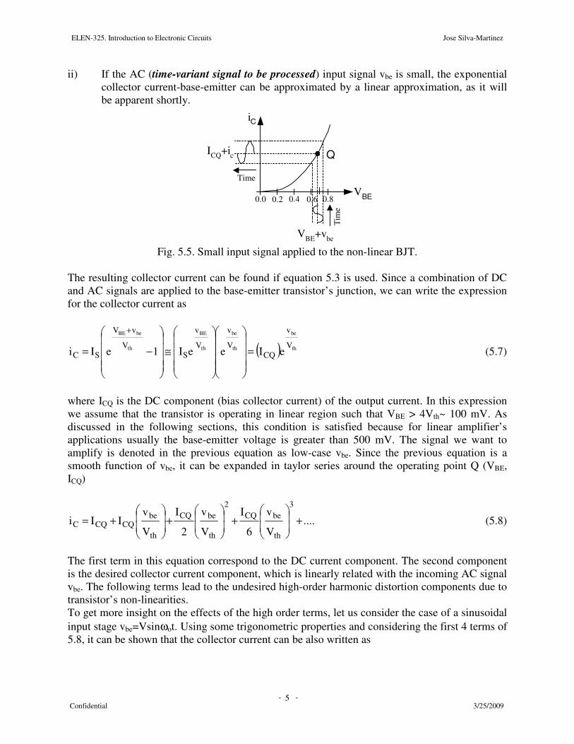
ii) If the AC (time-variant signal to be processed) input signal vbe is small, the exponential collector current-base-emitter can be approximated by a linear approximation, as it will be apparent shortly.
Q
VBE+vbe
ICQ+ic
Tim
e
Time
iC
VBE0.6 0.80.40.20.0
Fig. 5.5. Small input signal applied to the non-linear BJT.
The resulting collector current can be found if equation 5.3 is used. Since a combination of DC and AC signals are applied to the base-emitter transistor’s junction, we can write the expression for the collector current as
( ) th
be
th
be
th
BE
th
beBE
V
v
CQV
v
V
v
SV
vV
SC eIeeI1eIi =
≅
−=
+
(5.7)
where ICQ is the DC component (bias collector current) of the output current. In this expression we assume that the transistor is operating in linear region such that VBE > 4Vth~ 100 mV. As discussed in the following sections, this condition is satisfied because for linear amplifier’s applications usually the base-emitter voltage is greater than 500 mV. The signal we want to amplify is denoted in the previous equation as low-case vbe. Since the previous equation is a smooth function of vbe, it can be expanded in taylor series around the operating point Q (VBE, ICQ)
....V
v
6
I
V
v
2
I
V
vIIi
3
th
beCQ2
th
beCQ
th
beCQCQC +
+
+
+= (5.8)
The first term in this equation correspond to the DC current component. The second component is the desired collector current component, which is linearly related with the incoming AC signal vbe. The following terms lead to the undesired high-order harmonic distortion components due to transistor’s non-linearities. To get more insight on the effects of the high order terms, let us consider the case of a sinusoidal input stage vbe=Vsinωot. Using some trigonometric properties and considering the first 4 terms of 5.8, it can be shown that the collector current can be also written as

ELEN-325. Introduction to Electronic Circuits Jose Silva-Martinez
- - Confidential 3/25/2009
6
( )
( )
( )tsinVV
VI
tsinVV
V
V
I
tsinVV
VI
V
I
V
VIIi
opkth
pkCQ
opkth
pk
th
CQ
opkth
pkCQ
th
CQ
th
pkCQCQC
ω
+
ω
−
ω
++
+=
324
24
8
4
2
2
2
(5.9)
The transistor non-linearities result in a small variation of the DC component (first term of the previous equation) and the generation of undesirable signals (harmonic distortion components) located at multiple frequencies of the fundamental signal. The ratio of the amplitude of these unwanted signals to the desired component, proportional to the input signal, is defined as the harmonic distortion components. The first two harmonics are defined as
2
2
2
2
241
8
2433
41
8
422
≅
−
=ωω
=
≅
−
=ωω
=
th
pk
pkth
pk
th
CQ
th
CQ
pkth
pk
th
CQ
o
o
th
pk
pkth
pk
th
CQ
th
CQ
pkth
pk
th
CQ
o
o
V
V
VV
V
V
I
V
I
VV
V
V
I
@Amplitude@Amplitude
HD
V
V
VV
V
V
I
V
I
VV
V
V
I
@Amplitude@Amplitude
HD
(5.10)
The unwanted harmonic distortions reduce the quality of the output signal. Although the largest harmonic distortion is HD2, it can usually by suppressed by designing properly the system architecture (for instance this distortion is cancelled in fully-differential systems) but that is not the case of the third harmonic distortion. Notice that if we want to reduce the third harmonic component down to 1% of the fundamental component, then the peak value of the incoming signal Vpk must be limited to Vth/2=13 mV. For this reason we will limit the signals applied to the base-emitter terminal to vbe>10 mV, hence the circuit can be considered as a “linear” system. Using this approximation, the resulting transistor model is termed small signal model.

ELEN-325. Introduction to Electronic Circuits Jose Silva-Martinez
- - Confidential 3/25/2009
7
ICQ
ω0 2ω0 3ω0
ω
HD2HD3
0
Fig. Typical output current harmonic components. If the magnitude of the harmonic components are plotted in dB, HD2,3 can be easily found as the difference of the fundamental and the
component at 2,3ω0. Very simple but useful equations result if we assume that the magnitude of the AC signal is smaller than 0.4Vth (=10 mV). For this case, according to equation 5.8 the collector current can be approximated by a linear function of the AC base-emitter voltage given by
beth
CQCQC v
V
IIi
+= (5.11)
The collector current has fundamentally two components: the bias current ICQ and the AC current component that is linearly related to the base-emitter voltage signal. The parameter that is mapping the AC input voltage vbe (usually the information you want to process) into the output current is the first derivative of the IC-VBE curve evaluated at the operating point (ICQ, VBEQ), and it is given by ICQ/Vth. This parameter is defined as the small signal transconductance gain,
th
CQ
QBE
Cm V
I
vi
g =∂∂
= (5.12)
The small signal transconductance represents the slope of the linear approximation at the operating point, as shown in the following figure.
.
Q
VBEQ
ICQ
iC
VBE0.6 0.80.40.20.0
QBE
Cm v
ig
∂∂=
Fig. 5.7. Linear approximation for the transistor’s input characteristics at the operating point Q.
Around Q, the iC-vBE non-linear characteristic is approximated by a straight line with a slope given by ICQ/Vth.

ELEN-325. Introduction to Electronic Circuits Jose Silva-Martinez
- - Confidential 3/25/2009
8
The simplest transistor model can be obtained now. In the actual BJT, there is a forward biased diode connected between base and emitter. The base-emitter voltage controls the collector current that can be modeled as a voltage controlled current source; the resulting small signal model of the BJT is depicted in figure 5.8a. As aforementioned, the output current has both DC and AC components. The input’s diode can also be modeled as a DC voltage source in series with the diode’s resistance rπ. The base-emitter resistance rπ is determined by the base current as follows:
E
IC+gmvbeiB
B
C
iE
iC
E
IC+gmvbeiB
B
C
ie
ic
rπ
+ 0.7-
Fig. 5.8. Small signal model for the BJT: a) the base-emitter diode is shown and b) input’s diode
is represented by a DC voltage source and diode’s resistance.
th
BQ
QBE
B
V
I
v
i
r
1g =
∂
∂==
ππ (5.13)
Notice that both DC and AC signals are applied to the BJT’s input at the same time, and that the small signal parameters rπ and gm are determined by the DC operating point since these parameters are determined by the collector and base current derivatives evaluated at Q. For small signal conditions (amplitude of the base-emitter voltage |vbe|<10 mV) the transistor operates as a quasi-linear device. Under these conditions, we can use the superposition principle that applies to all linear systems, and analyze the circuit for two different cases: DC signals only and AC signals only. Although the analysis is split in two parts, it is worth mentioning that the output voltage consists of the two components. 5.4. Transistor Model and design considerations. DC analysis: Operating point and definition of the small signal parameters. The first analysis is carried out for DC signals only; hence the AC signals are made zero (short circuit the AC voltage sources and open the AC current sources) and the voltages and currents that define the operating point Q are obtained. The small signal parameters (e.g. rπ and gm) are determined from the DC operating point. The DC analysis of the circuit shown in figure 5.4 is carried out by making vbe=0, leading to the following results:
th
BEQ
V
V
SCQ eII = (5.14)

ELEN-325. Introduction to Electronic Circuits Jose Silva-Martinez
- - Confidential 3/25/2009
9
From this equation the VBEQ voltage determines the collector current, determining the operating point on the input characteristics; usually VBE is in the range 0.5-0.8 V. The collector-emitter voltage VCE is determined by both collector current and RC; from the circuit shown in fig. 5.4 with vbe=0 we can find that
VCC
RC
VBEQ+-
vCE0
+
-
iCQ
CCQCEQCC RIVV += (5.15) This is a linear relationship between VCE and IC, and static termed load line. For a given VBEQ, both equations 5.14 and 5.15 define the operating point Q (VBEQ, ICQ and VCEQ) of the amplifier, as shown in the figure 5.9a.
iC
VCE
QICQ VBEQ
VCC
VCC/RC
0.3 VCEQ
Load line
iC
VCE
Q2VBEQ
VCC
VCC/RC
0.3
RC increases
Q1Q3
(a) (b)
Fig. 5.9. Transistor’s output characteristics and load line: a) The operating point Q is defined by the selected VBEQ, ICQ and VCEQ; b) Effect of different load resistors RC for a fixed VBE.
Since both equations 5.14 and 5.15 determine the operation of the amplifier, the operating point Q is determined by the intersection of the transistor output characteristic associated with VBEQ and the line load. The load line is further determined by the power supply VCC and RC; the crossing point on the x-axis is in fact VCC. The slope of the linear equation 5.15 in the IC-VCE plane is given by -1/RC, therefore, the larger the resistor the smaller VCEQ is, as depicted in figure 5.9b. Notice that increase in RC decreases the slope pushing the operating point Q closer to the non-linear regime of the iC-vCE plane; this is not a good approach since the overall system could be very non-linear. It is always good practice to have the operation point Q within the flat region of the red curve in Figure 5.9b where VCE>0.3V. When an AC signal is added to the DC base-emitter voltage, the overall input voltage is modulated by that signal, as shown in Fig. 5.10. The operating point moves accordingly through the load line following the signal. The signal variations at the base-emitter junction are mapped to the VCE-axis generating the collector-emitter voltage. Since slope of the load line is given by 1/RC, hence the larger the collector resistor the larger the output signal is. RC however can not be

ELEN-325. Introduction to Electronic Circuits Jose Silva-Martinez
- - Confidential 3/25/2009
10
unconditionally increased because the operating Q moves to the saturation (very non-linear) region, and huge harmonic distortion components might be generated.
iC
VCE
Q
VCEQ
ICQ VBEQ
VCC
VCC/RC
0.3
linear range
vbe-peak
vce-peak
Fig. 5.10. The base-emitter voltage applied to the base-emitter junction modulates the operating
point, which moves over the load line as indicated by the blue arrow.
The selection of a proper operating point is one of the most critical design issues when designing linear amplifiers. The operating point Q must be selected based on the following observations: i) The operating point must be able to accommodate the signal variations. Since both DC
and AC signals are present at the same time, the overall collector-emitter voltage must operate such that 300 mV< VCEQ-vce-peak) and VCEQ+vce-peak)<VCC, otherwise the transistor might enter in the saturation region or the signal will be limited (clipped) by the supply voltage VCC.
ii) The AC parameters rπ and gm are determined by IBQ (=ICQ/β) and ICQ, respectively. The larger the DC current gain of the transistor (β) the smaller the base current is and the larger the base-emitter resistance rπ is. The collector current ICQ is computed from the required small signal transconductance gm which determines the amount of AC collector current generated by the AC input signal.
AC analysis: Transistor's ππππ-hybrid model. The second analysis is carried out for the AC signals only. The AC signals are applied to the circuit while the DC voltage sources are shorted and the DC current sources are considered as open circuits. This is the analysis that defines all AC system parameters such as input and output impedance, current and voltage gain and power gain. The simplified AC small signal model of the amplifier of fig. 5.8b is then simplified as shown in Figure 5.11a.
RC
vbe
v0
+
-
ic
E
rπgmvbeib
B
RC
ie
v0C
vbe
(a) (b)
Fig. 5.11. Equivalent circuit for AC analysis: a) AC equivalent short circuiting all DC voltage sources and opening the DC current sources and b) equivalent π-hybrid equivalent circuit.

ELEN-325. Introduction to Electronic Circuits Jose Silva-Martinez
- - Confidential 3/25/2009
11
The solution of this circuit can be obtained by using fundamental circuit analysis. The AC output voltage is given by the collector current times the load resistance RC. The base-emitter voltage is defined by the AC input signal then the computation for the voltage gain yields,
th
CCQCm
be
0
V
RIRg
v
v−=−= (5.15a)
Notice that the voltage gain is determined by the DC voltage drop (ICQRC) of the load resistor RC. As aforementioned, the larger the load resistor RC, the larger the small signal voltage gain is, but notice that what really matters is the product ICQRC. At room temperature, the thermal voltage is around 25 mV, hence previous equation can be simplified as
CCQth
CCQ
be
0 RI40V
RI
v
v−=−= (5.15b)
This result will be routinely used in the following sections. On the other hand, it should be noticed that the input impedance at the base terminal is equal to rπ(=Vth/IBQ). The smaller the base current the larger the input impedance is. Transistor's Output Impedance. Another effect present in the BJT is the collector current modulation due to the collector-emitter voltage. The collector current increases for large collector-emitter voltages because more carriers are attracted to the collector due to the higher electric field. If the base-emitter voltage is fixed, and the collector-emitter voltage is swept, we obtain the transistor’s output characteristics of the BJT. Extrapolating the current-voltage characteristics for negative collector-emitter voltages give us the so-called early voltage Vearly. The early voltage (crossing by zero voltage) is little sensitive to the bias conditions, and strongly depends on the technology used. Typical early voltages are in the range of 50-100 for standalone devices. The slope of the IC-VCE characteristics is defined as the transistor’s output conductance given by
iC
vCE-Vearly
g0
ICQ
0.3 vCEQ
QICQ/vearly
Fig. 5.12. iC-vCE characteristics of th BJT. The slope of the curves represents the transistor’s
output conductance go.

ELEN-325. Introduction to Electronic Circuits Jose Silva-Martinez
- - Confidential 3/25/2009
12
( ) early
CQ
earlyCEQ
CQ
QCE
C0
V
I
VV
I
v
ig ≅
−−=
∂
∂= (5.16)
In the previous equation we assume that the VCEQ << Vearly, which is a realistic assumption if discrete transistors are used, but this is not necessarily the case for integrated circuits. Taking the effect of the current modulation due to VCE into account, a more realistic model valid for AC signals only is depicted in Fig. 5.13a. The collector emitter resistor, given by rce=1/g0=Vearly/ICQ, is added. It will be evident in the following sections that this model is very useful for the analysis of common-emitter topologies wherein the emitter is connected to a DC voltage source or ground. However, for the analysis of other topologies is more convenient to use the T-model.
E
rπgmvbeib
B
C
rce
ie
ic
E
re
ie
αieibB
C
rce
ic
(a) (b)
Fig. 5.13. a) π-hybrid model for the BJT and b) T-model. Transistor's T-model. The T-model shown in Fig. 5.13b is based on the emitter terminal current representation rather than on the base terminal as the case of the π-model. If the transistor is analyzed from the emitter now, the current flowing through the emitter-base diode is the emitter current which is beta times the base current. Therefore the diode’s conductance seen from the emitter terminal is given by
th
EQ
QBE
Ee
V
I
v
ig =
∂
∂= (5.17a)
and the emitter resistance is
( ) ( )ββπ
+=
+==
1
r
I1
V
I
Vr
BQ
th
EQ
the (5.17b)
The collector current must be modeled as current-controlled current source iC=αiE. Another condition that must be added to this model is the KCL condition iE=iC+iB. By taking these equations into account, the equivalent T-model shown in Figure 5.13b results. The collector-emitter resistance is also included. Both models will be extensively used in the following sections. The models represent the same set of equations, and then the final results will be independent of the model used. The π-hybrid

ELEN-325. Introduction to Electronic Circuits Jose Silva-Martinez
- - Confidential 3/25/2009
13
model is very popular, but for some topologies it is easier to visualize circuit’s performances if the T-model is used. Practical Transistor Limitations. The models aforementioned are valid if and only if the transistor is operating in linear region. Some practical limits of the transistor model are: i) Transistor operating with very small collector emitter voltage (<300 mV) might operate in
the non-linear saturation region. Under this condition and if the base emitter voltage is large enough (~ 0.5 – 0.8 V), the input diode is on and huge base emitter can be generated. The collector current however is almost linearly related with VCE since the electric field between base and emitter terminals is not strong enough to attract the minority carriers that are traveling throughout the base. As a result, the collector current can be very small compared with the emitter current; both α and β current gain factors reduce drastically when the transistor is operated in saturation region. The transistor is quite inefficient if operated in that region; it is always recommended to maintain VCE > 300 mV under all possible operating conditions.
ii) Although the exponential behavior of the collector current is valid for several decades (in many cases from 0.1 µA till 10 mA) the collector current is limited due to second order effects such as parasitic resistor embedded in the transistor, velocity saturation of the carriers, and other second order effects. These effects reduce the current efficiency of the BJT at high current levels, limiting the current-gain factor especially for power amplifier applications. Current gain factors are also sensitive to temperature variations; the current-gain factor of the BJT looks as follows:
β
IC(mA)0.01
270
0.1 1.0 10 100
250
200
150
1100
-500
350
300
Fig. 5.14. Typical beta variations as function of collector current. Note that β is sensitive to
temperature variations. iii) Since all AC parameters rπ, gm and β are quite sensitive to temperature variations, it is critical
for most of the practical applications to reduce at much as possible these variations. Normalized sensitivity of the function H due to variations in T is defined as
T
TH
H
T
H
H
TSH
T ∆
∆
≅∂
∂= (5.18)

ELEN-325. Introduction to Electronic Circuits Jose Silva-Martinez
- - Confidential 3/25/2009
14
Therefore, the sensitivity function represents the ratio of the normalized variations of both H and T. Sensitivity of 1 means that the normalized variations on T affect in the same portion to the normalized transfer function H. 10 % normalized temperature variations will generate 10% normalized variation in the function H. iv) Very large base-emitter voltages lead to very large collector currents and huge temperature
gradients. Breakdown voltages in the junctions lead to drastic increments of the collector currents as well; the breakdown voltage VCE0 depends on the technology used, and the value can be found in the device data sheet provided by transistor’s manufacturer. It is strongly advisable not to reach the limits of power and voltages breakdown.
iC
VCEVCE0 Fig. 5.15. Transistors’ output characteristics; breakdown voltage effects are shown.
5.5. Basic amplifier configurations and equivalent circuits. 5.5.1. Common-emitter amplifier including the loading effects. The circuit shown in Figure 5.16a is known as the common-emitter amplifier, since the emitter is connected to a terminal with DC voltage signal only. When the AC analysis is carried out, as shown in Fig. 5.16b, that terminal does not play any role in AC circuit’s performance. The DC analysis of the circuit is similar to the one carried out for the previous example; make the AC signal zero (AC voltage sources are replaced by a short circuit and AC current source are considered open circuits). The fundamental equations to be solved are: For DC (operating point) analysis
th
BEQ
V
V
SCQ eII = (5.19) Solving the circuit for ICQ and VCE, the following equation results
CCQCEQCC RIVV += (5.20) This equation shows a linear relationship between ICEQ and VCEQ, and can plot on top of the transistor output characteristics, and define the static load line shown in fig. 5.17a. As aforementioned, for a given VBEQ, these equations define the operating point Q (VBEQ, ICQ and VCEQ) of the amplifier, as depicted in the figure 5.17a.

ELEN-325. Introduction to Electronic Circuits Jose Silva-Martinez
- - Confidential 3/25/2009
15
VCC
RC
vi
v0iC
CC
RL
VBEQ+- E
rπgmvbeib
B
RC
ie
C
vbe
v0
CC
RL
(a) (b)
Fig. 5.16. a) Common-emitter amplifier with load resistor and b) small signal equivalent circuit. For the AC analysis, the transistor must be replaced by the small signal model while the DC voltage and current sources are made zero; by doing that and according of the superposition principle, we can identify the AC response of the device without the effects of the DC sources. The small signal model of the amplifier including the load resistor RL and the coupling capacitor CC is depicted in fig. 5.16b. The equivalent circuit can be solved using the traditional circuit analysis methods; for instance, it can be shown that the output voltage is given by
( ) beCLC
CLCm0 v
CRRs1
CsRRgv
++−= (5.21)
The voltage gain transfer function shows a zero at DC and a pole determined by the addition of the two resistors RC+ RL and the series capacitor. Thus all low frequency signals will be attenuated by the zero until the pole’s frequency, as discussed in chapter II. For frequencies above the pole’s frequency, the voltage gain can be approximated by a simplified solution as follows
mLC
LC
beg
RRRR
vv
+−≅0 (5.22a)
Notice that the equivalent load impedance is given by the parallel of RC and RL; in fact, at high frequencies the capacitor presents very small impedance and can be replaced as a short circuit if its impedance is smaller than that of the resistors. Therefore the load impedance reduces the gain according to 5.22. Notice that 5.22a can also be expressed as
cLC
LCbem
LC
LC0 i
RRRR
vgRR
RRv
+−=
+−= (5.22b)
The implications are shown in figure 5.17b; the slope of the static load line (DC analysis) is defined by 1/RC but the AC voltage gain is defined by the slope of the dynamic load line, determined by 1/RC||RL according expression 5.22b. The load impedance RL reduces the voltage gain, therefore when cascading amplifiers for the design of very high gain solutions, it is important to increase as much as possible the input impedance of the next amplifier in order not to drastically reduce the gain of the precedent stage. Notice in Fig. 5.17 that the same base-

ELEN-325. Introduction to Electronic Circuits Jose Silva-Martinez
- - Confidential 3/25/2009
16
emitter voltage produces different output signal amplitude: while the blue lines in 5.17a are mapped into collector-emitter voltage by 1/RC, the dynamic load produces less amplitude variations due to the effect of RL.
iC
VCE
QICQ
VCC
VCC/RC
0.3
Static Loadline (1/RC)
VCEQ
VBEQ
iC
VCE
QICQ
VCC
VCC/RC
0.3 VCEQ
Static Loadline (1/RC)
Dynamic Loadline (1/RC||RL)
VBEQ
(a) (b)
Fig. 5.17. Transistor’s output characteristics and load line: a) The operating point Q is defined by the selected VBEQ, ICQ and VCEQ; b) Effect of different the load resistor RL for a fixed VBE.
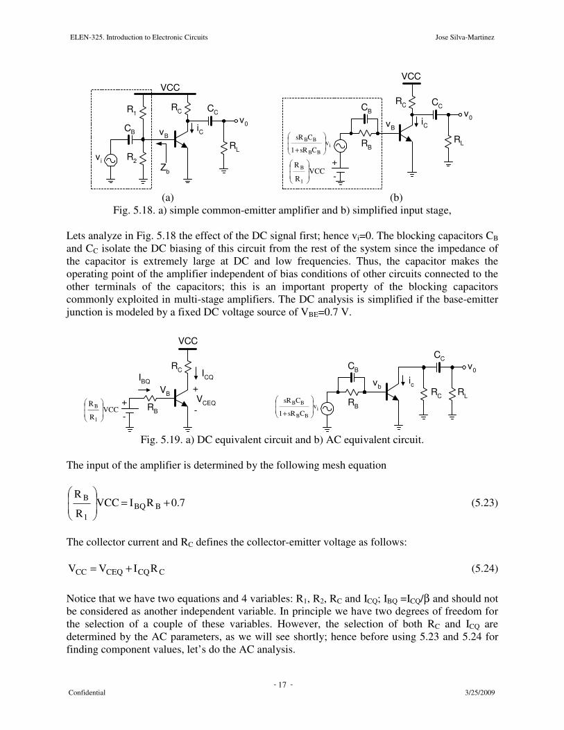
5.5.2. Common-emitter amplifier with resistive biasing. For the simplest common-emitter amplifier, the emitter terminal is connected to ground, while the incoming signal is applied to the base terminal as depicted in Fig. 5.18a. The DC base-emitter voltage is determined by the resistors R1 and R2, while the input signal is AC coupled through the use of CB. As a result, vB has two components: DC signal generated due to VCC and AC due to vi. To facilitate the analysis of this circuit, the input stage can be slightly modified using an equivalent circuit as shown in figure 5.18b. The equivalent thevenin’s voltage can be obtained by removing the BJT, and finding the voltage at node vB. To this end, and assuming that the circuit is quasi-linear, we can use superposition considering first the effect of VCC on that node; the AC signal vi must be short circuited. Since VCC is a pure DC signal, the capacitor operates as an open circuit and the equivalent voltage at the base terminal is given by VCC*R2/(R1+R2)= VCC*RB/R1 with RB=R1||R2. For the AC signal, we have to ground VCC and find the equivalent voltage at node vB; the resulting thevenin’s voltage is the result of a voltage divider between the blocking capacitor CB and RB. The equivalent impedance is computed by evaluating the impedance Zb seen from the base in the direction of the input signals; both vi and VCC must be grounded leading to an impedance consisting of RB||1/sCB. The resulting circuit is depicted in fig. 5.18b. Notice in this schematic that the effective voltage at the base of the transistor has in fact two components: one due to the VCC that defines transistor’s operating point, and a second one that is function of the AC signal vi to be processed. As discussed in the previous section, the superposition principle can be applied to any linear system; hence assuming that we operate the transistor in neighborhood around the operating point, the amplifier can be approximated in that vicinity as a quasi-linear device and the DC and AC operating modes can be independently analyzed. Notice that the output signal will be composed by both DC and AC components. Let’s split the analysis of the circuit considering each signal at a time.
ELEN-325. Introduction to Electronic Circuits Jose Silva-Martinez
- - Confidential 3/25/2009
17
VCC
vi
R1
R2
vBCB
Zb
RC
v0iC
CC
RL
VCC
RCv0iC
RB
vB
CBCC
RL
+
-
iBB
BB vCsR1
CsR
+
VCCR
R
1
B
(a) (b)
Fig. 5.18. a) simple common-emitter amplifier and b) simplified input stage,
Lets analyze in Fig. 5.18 the effect of the DC signal first; hence vi=0. The blocking capacitors CB and CC isolate the DC biasing of this circuit from the rest of the system since the impedance of the capacitor is extremely large at DC and low frequencies. Thus, the capacitor makes the operating point of the amplifier independent of bias conditions of other circuits connected to the other terminals of the capacitors; this is an important property of the blocking capacitors commonly exploited in multi-stage amplifiers. The DC analysis is simplified if the base-emitter junction is modeled by a fixed DC voltage source of VBE=0.7 V.
VCC
RC ICQ
RB
VB+
-VCC
R
R
1
B
+
-VCEQ
IBQ
RC
v0
ic
RB
vb
CB
CC
RL
iBB
BB vCsR1
CsR
+
Fig. 5.19. a) DC equivalent circuit and b) AC equivalent circuit.
The input of the amplifier is determined by the following mesh equation
7.0RIVCCR
RBBQ
1
B +=
(5.23)
The collector current and RC defines the collector-emitter voltage as follows:
CCQCEQCC RIVV += (5.24) Notice that we have two equations and 4 variables: R1, R2, RC and ICQ; IBQ =ICQ/β and should not be considered as another independent variable. In principle we have two degrees of freedom for the selection of a couple of these variables. However, the selection of both RC and ICQ are determined by the AC parameters, as we will see shortly; hence before using 5.23 and 5.24 for finding component values, let’s do the AC analysis.

ELEN-325. Introduction to Electronic Circuits Jose Silva-Martinez
- - Confidential 3/25/2009
18
The AC analysis is carried out by shorting the DC voltage sources (and opening the DC current sources if any). The resulting circuit is shown in Fig. 5.19b. The transistor can be replaced now by the small signal model; e.g. the model shown in Fig. 5.9b for first order computations. The analysis of the resulting circuit is straightforward: the base-emitter junction is modeled by the small signal resistor rπ, and then the voltage vbe is computed from Fig. 5.20 as:
RC
v0RB +
vbe-
CBCC
RL
iBB
BB vCsR1
CsR
+
E
rπ gmvbe
ie
CB
Fig. 5.20. Small signal model for the common-emitter amplifier.
( ) iBB
BB
Bi
BB
BB
BB
Bbe v
CR||rs1CsR
Rrr
vCsR1
CsR
CsR1R
r
rv
+
+=
+
++
=ππ
π
π
π (5.25)
This equation shows that the circuit behaves as a high-pass transfer function due to the zero located at ω=0 and the pole at ω=1/(rπ||RB)CB. The pole’s frequency is determined by the product of the blocking capacitor and the parallel of RB and the transistor’s input impedance rπ. For frequencies higher than the pole’s frequency, the transfer function tends to be 1; hence the base voltage becomes very similar to the input signal. Notice that the blocking capacitor blocks the DC voltage but also attenuates the signals with frequencies below the pole’s frequency. The pole’s frequency is given by 1/(rπ||RB)CB; since RB is usually much bigger than rπ, its value does not have too much effect on the pole’s location and pole is typically approximated as 1/rπCB, However, the bigger the blocking capacitor the lower the pole’s frequency is. As a result, very large capacitors are used to push down the pole’s frequency in order not to block important low frequency components. Notice that
( )
( ) BBBp
iiB
B
Bbe
CrCR||r
vvR||r
RRr
rv
p
ππ
ππ
πω>ω
≅=ω
=
+=
11
The output voltage is determined by the small signal transconductance and load impedance composed by the load resistors RL and RC as well as the coupling capacitor CC. The output voltage is found by solving the two nodal equations resulting at each side of CC ; since the analysis is straightforward, we do not provide the details here but it is advisable to solve the circuit and verify the following result.
ELEN-325. Introduction to Electronic Circuits Jose Silva-Martinez
- - Confidential 3/25/2009
19
( )( )
( ) ( )( ) iCm
BBB
BB
CLC
CL
beCmCLC
CL0
vRgRr
r
CR||rs1
CsR
CRRs1
CsR
vRgCRRs1
CsRv
+
+
++−=
++−=
π
π
π
(5.26)
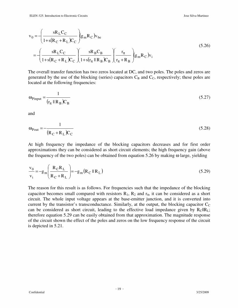
The overall transfer function has two zeros located at DC, and two poles. The poles and zeros are generated by the use of the blocking (series) capacitors CB and CC, respectively; these poles are located at the following frequencies:
( ) BBPinput
CR||r
1
π
=ω (5.27)
and
( ) CLCPout
CRR
1
+−=ω (5.28)
At high frequency the impedance of the blocking capacitors decreases and for first order approximations they can be considered as short circuit elements; the high frequency gain (above the frequency of the two poles) can be obtained from equation 5.26 by making ω large, yielding
( )LCmLC
LCm
i
0 R||RgRR
RRg
v
v−=
+−= (5.29)
The reason for this result is as follows. For frequencies such that the impedance of the blocking capacitor becomes small compared with resistors R1, R2 and rπ, it can be considered as a short circuit. The whole input voltage appears at the base-emitter junction, and it is converted into current by the transistor’s transconductance. Similarly, at the output, the blocking capacitor CC can be considered as short circuit, leading to the effective load impedance given by RC||RL; therefore equation 5.29 can be easily obtained from that approximation. The magnitude response of the circuit shown the effect of the poles and zeros on the low frequency response of the circuit is depicted in 5.21.

ELEN-325. Introduction to Electronic Circuits Jose Silva-Martinez
- - Confidential 3/25/2009
20
20 dB/dec
40 dB/dec
gmRC||RL
ωP1ωP2
ω
Fig. 5.21. Magnitude response for the common-emitter amplifier with blocking capacitors. Two poles are introduced: one defined by the input time constant, and the second one lumped to the
output’s time constant. To minimize the low-frequency bandwidth limitation, the blocking capacitors must be increased as much as possible. In case CB and CC are huge (infinite in the ideal case), the frequency of the poles is very small; hence the voltage gain is obtained replacing the capacitors by short circuits, and solving the reduced equivalent circuit. 5.6 Design example: A common-emitter amplifier. Design Example: Let’s consider the design of an amplifier with a high frequency gain of 34 dB. Let us to use the Q2N222 bipolar transistor; its small signal model is available on the SPICE parts. Some of the parameters of this transistor are: Beta (AC)= 150 (from BJT data sheet) Beta (DC)~ 150. These parameters can be extracted from spice simulations, but lets assume they are equal to 150 from previous characterization. Take these values as a reference, but make your own transistor characterization as follows. DC transistor’s characterization. Let us start with the characterization of the BJT. An easy setup based on two voltage sources is shown in the following figure.

ELEN-325. Introduction to Electronic Circuits Jose Silva-Martinez
- - Confidential 3/25/2009
21
Basic setup used for transistor’s characterization. For VCE> 0.3 V, sweeping VBE and measuring
IC, the output characteristics are generated. The input characteristics can be obtained by fixing the collector-emitter voltage VCEQ to a reasonable value such that the transistor operates in linear region (VCEQ > 300 mV). For this case, VCEQ = 1 V. The base-emitter voltage is swept from 0 up to 700 mV or more, then the input characteristics are obtained. The small signal transconductance can be obtained from this plot by finding the slope around the operating point, as shown in the following plot. Please compare the value obtained from the plot and the one computed as gm=40 ICQ (=48 mA/V @) ICQ=1.2 mA).
V_vbe
500mV 550mV 600mV 650mV 700mV IC(Q8)
0A
4.0mA
8.0mA
Input characteristics for the selected BJT: IC vs. VBE; VCEQ = 1 V for this case.
gm
ELEN-325. Introduction to Electronic Circuits Jose Silva-Martinez
- - Confidential 3/25/2009
22
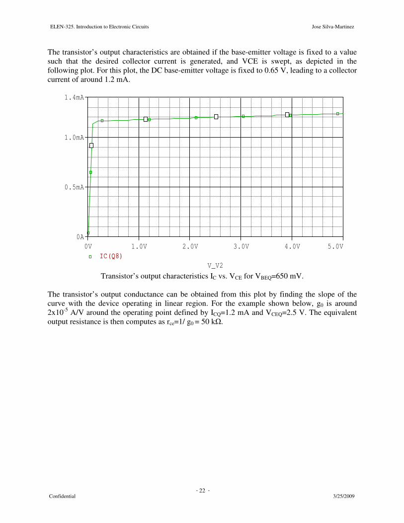
The transistor’s output characteristics are obtained if the base-emitter voltage is fixed to a value such that the desired collector current is generated, and VCE is swept, as depicted in the following plot. For this plot, the DC base-emitter voltage is fixed to 0.65 V, leading to a collector current of around 1.2 mA.
V_V2
0V 1.0V 2.0V 3.0V 4.0V 5.0V IC(Q8)
0A
0.5mA
1.0mA
1.4mA
IC(Q8)
Transistor’s output characteristics IC vs. VCE for VBEQ=650 mV.
The transistor’s output conductance can be obtained from this plot by finding the slope of the curve with the device operating in linear region. For the example shown below, g0 is around 2x10⁻⁵ A/V around the operating point defined by ICQ=1.2 mA and VCEQ=2.5 V. The equivalent output resistance is then computes as rce=1/ g0 = 50 k.

ELEN-325. Introduction to Electronic Circuits Jose Silva-Martinez
- - Confidential 3/25/2009
23
V_V2
0V 1.0V 2.0V 3.0V 4.0V 5.0V IC(Q8)
1.10mA
1.15mA
1.20mA
1.25mA
1.30mA
IC(Q8)
Output Characteristics Zoom-in: Output resistance/conductance can be extracted from this plot.
The input impedance is obtained by plotting iB vs. vBE, as shown in the following simulation. The transistor’s input resistance rπ is (=Vth/IBQ) is obtained by finding the slope of the curve at the proper base-emitter voltage (0.65 V for this example).
V_vbe
600mV 620mV 640mV 660mV 680mV 700mV IB(Q8)
0A
25uA
50uA
IB(Q8)
go
gππππ

ELEN-325. Introduction to Electronic Circuits Jose Silva-Martinez
- - Confidential 3/25/2009
24
IB-VBE characteristics for the selected BJT: Input conductance gπ and input impedance rπ (= 1/ gπ)can be obtained from this plot.
Other important parameters are the static current gain β-DC and the dynamic current gain gain β-AC. The former parameter must be used for the computation of the DC-operating point, and it is defined as the ratio of ICQ to IBQ; in the following simulation, at ICQ=5 mA β-DC is approximately given by 5mA/30 µA=166. The dynamic current gain relates the AC collector current and the AC base current, therefore it has to be used whenever AC analysis is carried out. β-AC (=∆ICQ/∆IBQ) around ICQ=5 mA is computed as 0.7mA/0.4 µA=175.
IB(Q8)
0A 10uA 20uA 30uA 40uA 50uAIC(Q8)
0A
4.0mA
8.0mA
IC-IB characteristics: β-DC (=ICQ/IBQ) and β-AC (=∆ICQ/∆IBQ) can be obtained from this plot.
5.6.2. Example: DESIGN PROCEDURE. A particular case of the common-emitter amplifier previously discussed is shown below. Let’s use this topology for the design on an amplifier: the required voltage gain is 34dB (53.8). In a first approximation the voltage gain is given by equation 5.29: |AV|=gmR4=ICQ*R4/Vth, therefore
V4.1mV26*8.53RI 4CQ == For a collector current of 1.4 mA, the required output impedance is around 1K. Although the selection of the collector current is arbitrary in this example, the selection of the load impedance is quite critical and it should be selected based on the value of the input impedance of the following stage. The selection of the collector current and transistor’s β defines the base current and the input resistance rπ, however, at this stage of the discussion we would like to focus the attention on the use of the equations aforementioned.
ββββ_AC

ELEN-325. Introduction to Electronic Circuits Jose Silva-Martinez
- - Confidential 3/25/2009
25
For a collector current ICQ=1.4 mA, and if βDC is around 150, then A33.9I
IDC
CQBQ µ=
β= . In a
first approximation, the resistance R1connected at the transistor’s base can be computed as:
Ω=−
= − K46210x3.9
7.051R
6
Let us simulate the circuit in SPICE and analyze the operating point (DC currents and voltages). The results are depicted in the previous schematic.
Common-emitter amplifier selected for this example
Important Observations:
1. Voltage drop across R4 is 1.5V and we were expecting 1.4 V; then the expected voltage gain, (= 40ICQR4) could be slightly greater (35.2 dB) than required.
2. The actual VBE =0.655 is less than the 0.7 V used in our previous computations. Then obviously we have to re-calculate R1 accordingly.
3. Since the voltage across R1 is greater than expected, the base current is greater than computed and this is the reason for the larger collector current. Before we re-calculate the amplifier’s components, le us simulate the circuit and find-out circuit’s response.

ELEN-325. Introduction to Electronic Circuits Jose Silva-Martinez
- - Confidential 3/25/2009
26
Using the SPICE AC analysis option, the following results were obtained. The circuit has a low-frequency pole; according to our previous discussion it is defined by the capacitor C1 and the parallel of R1 and rπ. The base resistance rπ is around 2.6 k and dominates the value of the input impedance, thus the location of the pole is around 1/ rπC1=370 rad/sec (= 60 Hz). The medium-band frequency gain is around 35 dB; not bad at all but the ideal gain= 34.6 dB. Let’s find out the reasons of this discrepancy.
Frequency
100Hz 1.0KHz 10KHz 100KHz 1.0MHz 10MHz 100MHzVDB(R4:1)
20
25
30
35
VDB(R4:1)
For the second iteration it is IMPERATIVE that you check the transistor’s parameters. This can be done in PSPICE if you analyze the OUTPUT FILE. UNDER ANALYSIS YOU CAN SELECT THE OPTION “EXAMINE OUTPUT”. This option is quite important since precise AC and DC parameters are given there! The following is a piece of the information you can find in that option.
NAME Q_Q8 MODEL Q2N2222
IB 9.40E-06 IC 1.49E-03
VBE 6.55E-01 VBC -2.85E+00 VCE 3.51E+00
BETADC 1.59E+02 GM 5.74E-02 RPI 3.04E+03 RX 1.00E+01 RO 5.15E+04

ELEN-325. Introduction to Electronic Circuits Jose Silva-Martinez
- - Confidential 3/25/2009
27
CBE 6.02E-11 CBC 4.28E-12 CJS 0.00E+00
BETAAC 1.74E+02 CBX/CBX2 0.00E+00
FT/FT2 1.42E+08
Use the proper ββββ_DC and VBEQ, and find the value for R1. Collector current is defined by base-emitter current, then the priority is to adjust base current based on R1, VBE and DC-β. In the DC-simulation that adjusting R1, the collector current and collector voltage are closer to the expected DC value (VCEQ_ideal =3.6 V). It is expected to have more accurate results this time. The circuit was re-simulated in SPICE, and the AC results are shown in the following plot; the AC-gain is 34.6 dB, which is close enough to our expected results.

ELEN-325. Introduction to Electronic Circuits Jose Silva-Martinez
- - Confidential 3/25/2009
28
Frequency
100Hz 1.0KHz 10KHz 100KHz 1.0MHz 10MHz 100MHzVDB(R4:1)
20
25
30
35
VDB(R4:1)
Second iteration: Ideal gain= 34.6 dB; we are really close to the expected results.
5.6.3 Characterization procedure using SPICE and design examples. To design a good amplifier is not an easy task, since it depends on many factors. Usually there is not a universal solution but a good engineer must be able to find a good trade-off between performances and cost in terms of power and silicon area. In most of the practical cases the solution must be tailored according to system specifications. The amplifier’s design procedure involves several fundamental steps: i) Understand the problem and obtain the specifications for your design. Before you start
your design, obtain the most important amplifier specs: required input impedance, required output impedance, required voltage/current/power gain, and estimate the expected signal swing at various amplifier stages. This step is fundamental for the selection of components and technologies to be used.
ii) Characterization of transistors. The component vendors provide the technical information of the devices; please check the specs of all components to be used. It is advisable to make a rough SPICE characterization of your active devices using the proper models.
iii) Select proper components and devices. This is an application dependant selection. You must be sure that both passive and active devices operate properly for the given specs; e.g. maximum frequency of operation, power dissipation, supply voltages, expected signal swing, impedance matching, etc.
iv) THE MOST CRITICAL DECISION IS THE SELECTION OF THE OPERATING POINT. The amplifier’s gain, frequency response and power dissipation are determined by the selected operating point; be sure that the transistor operates properly when you connect it to the previous and next stage. Very often the stand alone circuit works fine but due to finite impedances of previous and next stages the performance of the circuit is degraded

ELEN-325. Introduction to Electronic Circuits Jose Silva-Martinez
- - Confidential 3/25/2009
29
when it is incorporated to the whole system; both DC and AC characteristics might be affected.
v) First approximation (hand calculations). This is the starting point for the design. We first assume a very simple model for the active devices such as VBEQ=0.7 V for the BJT. The main goal at this stage of the design is to have a first approximation to our main target. Write down the fundamental AC equations for the selected amplifier:
a. Input impedance b. Output impedance c. Transmission gain d. Poles and zeros (if needed)
vi) Check your first design in SPICE. Since the models we used for the hand calculations, we have to simulate our circuit in SPICE and compare both simulations and hand calculations. Check transistor’s parameters for the selected operating point, and identify the critical deviations. In case your final solution is not correct, think about the following issues:
a. Is the selected transistor good enough for your application? b. Are your assumptions reasonable? c. Where is the main design issue? d. How to overcome it?
vii) Re-evaluate your specs/assumptions/architecture. Re-calculate all your amplifier’s components. Check the real VBEQ voltage for the transistor(s) and current gain (beta). Use the values given by SPICE and re-calculate all components.
viii) Check your final design with SPICE. You need at least 2 iterations to come up with a reasonable solution.
5.7. Common-emitter amplifier with emitter degeneration resistors. The most general common-emitter configuration is shown below in Fig. 5.22. The DC operating point is more robust if additional resistors are added at the emitter terminal. As will be evident in the following discussion, these resistors make the circuit less sensitive to temperature variations and allow us to have full control on the operation point. A drawback of this topology is that the resistors RE1 and RE2 decrease the small signal voltage gain. A large capacitor (CE) eliminates the effect of RE2 on the voltage gain but it is used for DC stabilization. As discussed in previous sections, the AC input resistance is increased due to emitter resistance added.
VCC
RC
vi
vC
RB1
RB2
vB
RE1
RE2 CE
CBRS
RL
V0
CL
Fig. 5.22. General configuration of the common-emitter amplifier.

ELEN-325. Introduction to Electronic Circuits Jose Silva-Martinez
- - Confidential 3/25/2009
30
5.7.2. DC and AC equations. The DC-equivalent circuit of the general common-emitter amplifier is shown in Fig. 5.23a. Similarly to the previous circuits, the operating point is determined by the following set of equations
( ) ( )
( )
α+
++=+++=
=
+
α+
β+=+++=
2E1ECCQCEQ2E1EEQCCQCEQ
2B1BB
2E1EB
CQ2E1EEQBBQ1B
B
RRRIVRRIRIVVCC
R||RR
RR1R
I7.0RRI7.0RIVCCRR
(5.30)
VCC
RCRB1
RB2
vB
RE1+RE2
VCEQ
ICQ
IEQ
+
-
vi
RE1
reie
αieZi RCIIRL
V0
RB
ib
(a) (b)
Fig. 5.23. Common-emitter amplifier with source degeneration: a) DC equivalent circuit and b) small signal model for AC analysis. The source resistance RS is considered very small and it is
ignored in the AC analysis. The AC analysis of the topology is a bit more complex due to the resistor RE1 connected at the emitter of the transistor; just not to complicate the analysis of this topology, we consider the case RS=0, but it will be apparent at the end of this subsection that its effect can be easily incorporated to our results. It is easier to analyze the circuit if the T-model is used; the small signal circuit is shown in Fig. 5.23b; for first order computations we ignore the effect of the collector-emitter resistance. To get more insight on the benefits of adding RE1, let us compute the input impedance of this topology. The input impedance seen through the base of the amplifier can be computed as
( )( ) ( ) 1E1Eee
i
b
ii R1rRr1
1
iv
i
vZ β++=+β+=
β+
== π (5.31)
A very desirable effect of the resistor RE1 is the increment of the impedance seen from the base by a factor (1+β)RE1; input impedance is further increased by adding more emitter degeneration. If large input impedance is required, the resistors RB1 and RB2 must be increased as well because the total impedance seen by the input voltage source vi is the parallel of Zi and RB. From the small signal equivalent circuit, the amplifier’s voltage gain is determined by the following expressions

ELEN-325. Introduction to Electronic Circuits Jose Silva-Martinez
- - Confidential 3/25/2009
31
( )LCe0 RRiv α−= (5.32) and the AC emitter current is computed as
i1Em
m
1Em
i
1Ee
ie v
Rg
g
Rg
v
Rr
vi
+α=
+α
=+
= (5.33)
Therefore, the overall voltage gain is obtained as
( )1Em
LCm
i
0V
Rg
RRg
v
vA
+α
α−== (5.34)
A drawback of the emitter degeneration (resistor RE1) is that the voltage gain is reduced due to the term gmRE1. Whenever we use the emitter degeneration resistor, there is a design trade-off: the larger the resistor RE1 the larger the input impedance is, as shown by equation 5.31, but the smaller the voltage gain is as well, as can be seen in equation 5.33. This trade-off is unavoidable in BJT based circuits, and the emitter resistance RE1 must be judiciously selected to satisfy input impedance constraints without too much degradation in the voltage gain. Another benefit of the emitter degeneration is its low sensitivity to temperature variations: remember that β, gm, rπ and re are temperature sensitive parameters. At room temperature we have the following simplified expression
( )1ECQ
LCCQV
RI*401
RRI*40A
+−≅ (5.35)
Where we assume that α is very close to 1. If a robust solution is required, it is advisable to design the circuit such that 40*ICQRE1 >>1 (actually 4-8 times larger than 1 is often used); in that case this expression can be further reduced, leading to the following reduced equation
1E
LCV
R
RRA −≅ (5.36)
This result shows that if enough emitter degeneration is used, the voltage gain is not very sensitive to the temperature’s sensitive transistor parameters such as rπ, re or gm. The voltage gain mainly depends on the ratio of the load impedance RC||RL and the emitter degeneration resistance RE1. Although it is not clear at this stage of the course, the emitter degeneration is a kind of feedback similar to the one used in OPAMP based circuits, that leads to an overall voltage gain that depends on the ratio of auxiliary elements (feedback and input impedances attached to the OPAMP) used rather than on the parameters of the OPAMP. A design example based on this circuit is discussed in the next section.
![Junction Transistor (Revision with Ques.) · [9 ] BJT FET BJT (bipolar junction transistor ) is the bipolar device FET (field effect transistor) is a uni - polar device Its operation](https://img.pdfslide.net/doc/110x75/5e080e954f3d5f6410302f8e/junction-transistor-revision-with-ques-9-bjt-fet-bjt-bipolar-junction-transistor.jpg)