Embed Size (px)
Citation preview

93
Abstract A comprehensive overview of density functional theory simulations of high-k oxide/III-V semiconductor interfaces is presented. The methodologies of realistic amorphous high-k oxide generation by hybrid classical-DFT molecular dynamics are compared. The simulation techniques, oxide/semiconductor model designs and rules for formation of unpinned high-k oxide/semiconductor interfaces are discussed. The density-functional theory molecular dynamics simulations of a-Al 2 O 3 /InGaAs and a-Al 2 O 3 /InAlAs/InGaAs stacks are presented and analyzed.
5.1 Introduction
5.1.1 High-k Oxides
The rapid scaling of complementary metal oxide semiconductor (CMOS) technol-ogy requires substituting the traditional gate oxide, silicon dioxide (SiO 2 ), with high-k dielectrics, which can maintain the same capacitance with much lower leak-age current. Silicon dioxide was the major gate oxide material for decades. Since transistors have been rapidly decreasing their lateral sizes to increase surface den-sity of microelectronic elements on the chip area, the gate oxide had to decrease its thickness to scale the capacitance, drive current, and device performance. However, decreasing SiO 2 thickness below 7–13 Å is not feasible since it leads to signifi-cant tunneling leakage, increased power consumption, and deterioration of device reliability [ 1 , 2 ]. Replacement of SiO 2 oxide by high-k materials would allow an increase in gate oxide capacitance while diminishing the gate leakage.
The gate oxide in a Metal-Oxide-Semiconductor-Field-Effect-Transistor (MOSFET) can be considered as a parallel plate capacitor. Ignoring quantum
S. Oktyabrsky, P. D. Ye (eds.), Fundamentals of III-V Semiconductor MOSFETs , DOI 10.1007/978-1-4419-1547-4_5 , © Springer Science+Business Media LLC 2010
Chapter 5 Density Functional Theory Simulations of High-k Oxides on III-V Semiconductors
Evgueni A. Chagarov and Andrew C. Kummel
E. A. Chagarov ( � ) Department of Chemistry and Biochemistry , University of California , San Diego, La Jolla, California 92093 , USA e-mail: [email protected]

94 E. A. Chagarov and A. C. Kummel
mechanical interaction and depletion effects at the oxide/semiconductor and oxide/electrode interfaces, the capacitance C of the gate oxide approximated as the paral-lel plate capacitor can be given by:
C = kε0S
d, (5.1)
where S is a capacitor plate area, d is a distance between capacitor plates (equal to capacitor oxide material thickness), k is a relative dielectric constant, and � 0 is the electrical permittivity of vacuum. As follows from Eq. (5.1), using a material with high dielectric constant k would allow an increase of oxide thickness while avoiding the problem of oxide current leakage and maintaining the same capacitance per unit area required for a high density of MOSFET devices on the chip surface.
Replacing SiO 2 by high-k gate oxide materials adds a whole plethora of new tech-nological challenges to the device manufacturing process. Besides a high dielectric constant, the selected high-k gate oxide material should satisfy a whole range of additional requirements, such as proper band alignment to the semiconductor sub-strate, thermal stability, low interface roughness and associated with it high mobility of charge carriers, and low density of electrical defects in the oxide/semiconductor interface.
Currently, the most promising high-k gate oxide materials are hafnium diox-ide (HfO 2 ), zirconium dioxide (ZrO 2 ), alumina (Al 2 O 3 ), hafnium silicate (HfSiO 4 ), and zirconium silicate (ZrSiO 4 ) [ 3 – 6 ]. In the real-world oxide gate/semiconductor stacks, these materials are often found in amorphous phases due to deposition and post-deposition processing.
5.1.2 III-V Semiconductors
The III-V semiconductors are very promising materials for microelectronic and optoelectronic applications. They can provide much higher low field carrier mobil-ity than Si-based devices and, therefore, are potentially beneficial for high-speed applications. The III-V semiconductors are compound semiconductors formed by chemical elements from groups III and V. In the crystal structure of III-V semicon-ductors, every atom of group III is bound to four group V atoms while every group V atom is bound to four group III atoms. The bonding model of III-V semiconduc-tors is mainly covalent with moderate bond ionicity due to the modest electronega-tivity difference between group III and V elements. The III-V semiconductors can form binary, ternary, quaternary and even higher-order compounds mixing different number of III and V group elements. The mixing of various III and V group ele-ments in one semiconductor compound provides wide possibilities for engineering of the semiconductor band-gap and the associated emission/adsorption wave-length, which are critically important properties for microelectronic and optoelectronic applications. Among binary III-V semiconductors, the most widely investigated are InAs, GaAs, InP, GaP, and their ternary alloys. Among III-V semiconductors,

955 Density Functional Theory Simulations of High-k Oxides on III-V Semiconductors
the typical technologically promising compounds include In x Ga 1�x As, In x Al 1�x As, Al x Ga 1�x As, and In x Ga 1�x P.
5.1.3 Density-Functional Theory
The Density-Functional Theory (DFT) is an extremely successful quantum-mechanical first-principles technique capable of modeling the electronic structure of many-body atomic, molecular and condensed matter systems. DFT is based on the Kohn-Sham theorems and equations [ 7 , 8 ], which reduce the many-body prob-lem for N particle system to a one-parameter problem using the density-functional approach when the energy functional of the system can be described in terms of charge density as follows:
E[ρ] = T [ρ]+∫
Vext(r)ρ(r)dr + VH [ρ]+ Exc[ρ] , (5.2)
where T is the kinetic energy of the system, V ext is the external potential acting on the system (e.g., due to ions), E xc is the exchange-correlation energy, and V H is the Hartree (electron-electron interaction) energy given by:
VH[ρ(r)
] = 1
2
∫ρ(r)ρ(r′)|r − r′| drdr′. (5.3)
In practical applications, DFT codes use the variational approach: the wavefunction representation is varied to minimize the system total energy until it is numerically converged to the ground state energy and charge density. The major problem of DFT is that the exchange-correlation functionals, E xc are known exactly only for the free electron gas, but in all other more general cases, they have to be approximated. One of the classical approximations is the local-density approximation (LDA), where the exchange-correlation functional is determined only locally by the electron den-sity at the given spatial point. The generalized gradient approximation (GGA) is the next refinement of LDA; while GGA is still a local approximation, it takes into account the gradient of the charge density at the given spatial point thereby making it more accurate for systems with steep spatial charge-density variations. Although for the majority of cases, DFT results show strong correlation to experimental data, standard DFT approaches (including LDA and GGA) still demonstrate problems with reproduction of the true band-gaps of solid phases, intermolecular interactions (especially van der Waals interaction), transition states and charge transfer excita-tions. To overcome these limitations, a set of improvements has been proposed for the standard DFT methodology. An excellent in-depth overview of DFT and other electronic structure methods can be found elsewhere [ 9 ].

96 E. A. Chagarov and A. C. Kummel
5.2 Methodology of DFT Simulations of High-k Oxides on Semiconductor Substrates
Si has been the major semiconductor substrate for several decades which made it the focus of active DFT research for potential high-k oxide/semiconductor stack applications [ 3 – 5 , 10 – 35 ]. Ge due to its high hole mobility and similarity to Si was also actively investigated as a potential substrate for high-k oxides [ 6 , 36 – 38 ]. This chapter will give brief overview of DFT simulations of high-k oxides on Si or Ge concentrating mainly on methodology. The DFT simulations of oxide/semiconduc-tor interfaces can be performed using different computational approaches to initial system design and different simulation algorithms.
5.2.1 Oxide Deposition Technique in DFT Simulations
The initial system configuration is extremely important factor which can signifi-cantly influence the final outcome of oxide/semiconductor simulations. There are several computational techniques for oxide deposition on the semiconductor sub-strate which can be employed to devise the initial interfacial structure.
1. Kinetic Monte-Carlo (KMC) simulations [ 39 – 41 ]. KMC simulations can model the time evolution of physical and chemical processes occurring with a given rate. These rates are input variables for KMC simulations and are often obtained from DFT simulations of the energy barriers for certain system transitions.
2. Density-Functional Theory Molecular Dynamics (DFT MD) simulations can be employed to simulate oxide molecules randomly bombarding the semiconduc-tor surface simulating experimental molecular beam, e-beam, or sputter deposi-tion. Since nearly all oxides including Al 2 O 3 and ZrO 2 evaporate incongruently, this approach can only provide very approximate description of oxide molecular beam deposition.
3. Artificial layer-by-layer deposition of oxide atoms without any correlation to real deposition speed followed by molecular dynamics annealing and/or relaxa-tion can be used to simulate reactive oxide formation on semiconductors. For example, to investigate thermal oxidation by O 2 , DFT can be used to simulate a very rapid reaction with atomic oxygen.
4. DFT molecular dynamics simulations with previously prepared bulk oxide sam-ple stacked to the semiconductor surface and relaxed or annealed-cooled-relaxed can be employed to simulate experimental postdeposition-annealed oxide/semi-conductor interfaces. The oxide bulk sample can be thoroughly tested prior to main oxide-semiconductor simulations. This method is the most realistic for sys-tems in which the oxide and semiconductor are weakly interacting.
5. Hybrid methods mixing molecular dynamics and Monte-Carlo techniques can be employed to simulate different processes with various rates during deposition by different approaches.

975 Density Functional Theory Simulations of High-k Oxides on III-V Semiconductors
Each of these methods has its own advantages and disadvantages, which should meet certain strict criteria of applicability, such as realism, computational efficiency, and achievable simulated timescale.
Method A: Kinetic Monte-Carlo simulations are computationally efficient and can simulate atom-by-atom deposition at long timescale. However in comparison with DFT MD, KMC simulations provide lower accuracy for atomistic modeling of oxide-semiconductor interface evolution because KMC simulations replace the true atomic dynamics with statistically-equivalent MC kinetics. The KMC simulations are based on a set of energy barrier calculations and associated rates for various configurations and transitions between the configurations. The computer simula-tions of oxide/semiconductor interfaces often involve significant deformation in the substrate, interface, and oxide regions with a very large number of degrees of freedom. An attempt to reproduce the realism of such oxide-semiconductor simu-lations with 3D KMC would require taking into account an unrealistic number of atomic configurations, transition barriers between the numerous configurations, and multiple DFT-calculated activation energies.
Method B: DFT-MD simulations modeling oxide atoms randomly bombarding the semiconductor surface cannot accurately reproduce experimental oxide-semi-conductor interface growth for three reasons: (a) Most gate oxides are deposited by atomic layer deposition (ALD), not molecular beam deposition. (b) The times-cale needed to deposit 100 atoms of oxide at realistic experimental deposition rate requires many orders of magnitude longer timescale than picoseconds, which mod-ern DFT MD can afford. The typical MBE deposition rate is ~1.0 ML/s [ 42 ], the fastest MOCVD is ~3 ML/s [ 43 ] and the fastest sputtering deposition is ~1 ML/s [ 44 ]. (c) With the exception of LaAlO 3 , nearly all common gate oxides evaporate incongruently; therefore, to form stoichiometric films using molecular beam depo-sition, a second oxygen source or post-deposition annealing must be employed.
Method C: Artificial layer-by-layer deposition of oxide atoms without any cor-relation to real deposition speed followed by molecular dynamics annealing and/or relaxation somewhat circumvents the problem of deposition speed. The technique works best when certain general bonding rules for the given chemical species are employed. This approach was successfully used by Hakala et al. for modeling of HfO 2 growth on Si substrate [ 24 ].
Method D: DFT molecular dynamics simulations with a previously prepared bulk oxide sample stacked to the semiconductor surface and relaxed or annealed-cooled-relaxed, provides much more elaborate system of checks to verify high quality of the crystalline or amorphous oxide sample prior to bonding to the semiconductor. Although methods (A), (B), and (C) are able to simulate atom-by-atom deposition they raise significant concerns about oxide film realism, especially if amorphous oxide films are investigated. The random deposition of atoms for relatively small atomistic system and limited statistical ensemble can produce significant devia-tions in oxide sample properties. Because of the checks to verify the quality of the amorphous oxide samples, method (D) often provides a realistic affordable compu-tational alternative to methods (A), (B), and (C) for simulating amorphous oxide-semiconductor interfaces when the interfacial reactions are limited. The technique

98 E. A. Chagarov and A. C. Kummel
has been successfully used by many groups for atomistic simulations of oxide-semi-conductor interfaces. Tse et al. successfully utilized this approach for modeling of ZrO 2 /Ge [ 6 ]. Peacock et al., Puthenkovilakam et al., Fonseca et al. and Dong et al. successfully applied it to simulations of ZrO 2 /Si, ZrSiO 4 /Si and HfO 2 /Si interfaces [ 4 , 13 , 16 , 18 , 45 , 46 ]. Zhang et al., Peacock et al., Robertson et al., and Forst et al. used it for modeling of SrTiO 3 /Si interface [ 14 , 20 , 47 , 48 ]. Broqvist et al. and Capron et al. used it for simulations of a-HfO 2 /a-SiO 2 /Si and HfO 2 /SiO 2 stacks [ 11 , 33 , 34 ], Chagarov et al. used it for simulations of a-Al 2 O 3 /Ge, a-ZrO 2 /Ge, a-Al 2 O 3 /InGaAs and a-Al 2 O 3 /InAlAs/InGaAs [ 36 , 37 , 49 , 50 ].
Method E tries to combine best of molecular dynamics and Monte-Carlo approaches. In this approach, all processes in the system are classified by their characteristic times (rates). The low barrier processes, which typically involve bulk and surface relaxations are described by MD simulations (classical or first-principle), while high-barrier processes like surface reactions, activation diffu-sion and similar are treated by Monte-Carlo family approaches. Knizhnik et al. successfully applied such hybrid approach to simulations of ZrO 2 deposition on Si(100) surface [ 29 ]. In their study, the system relaxation was modeled by classi-cal MD with empirical potentials, while high-barrier processes were simulated by Kinetic Monte-Carlo approach. The Ng et al. used a similar technique to model oxidation kinetics of Si(100)-SiO 2 interface [ 51 ]. In the latter case, the system relaxation processes were simulated by DFT while high-barrier processes were modeled using the Metropolis algorithm. Hybrid methods (E) can simulate much longer timescales than standard molecular dynamics and better handle systems with high lattice irregularities like amorphous films; however, they still inherit original problems of the underlying techniques such as replacement of the true atomic dynamics with statistically-equivalent MC kinetics which inevitably intro-duces additional error in the final configuration. Although it is able to provide high degree of realism, molecular dynamics with its typical timestep of ~1 fs still has serious limitations on simulated timescale. The final choice of the oxide/semi-conductor deposition technique remains a difficult compromise between accu-racy, timescale, and computational efficiency.
5.2.2 Oxide-Semiconductor Stack Design
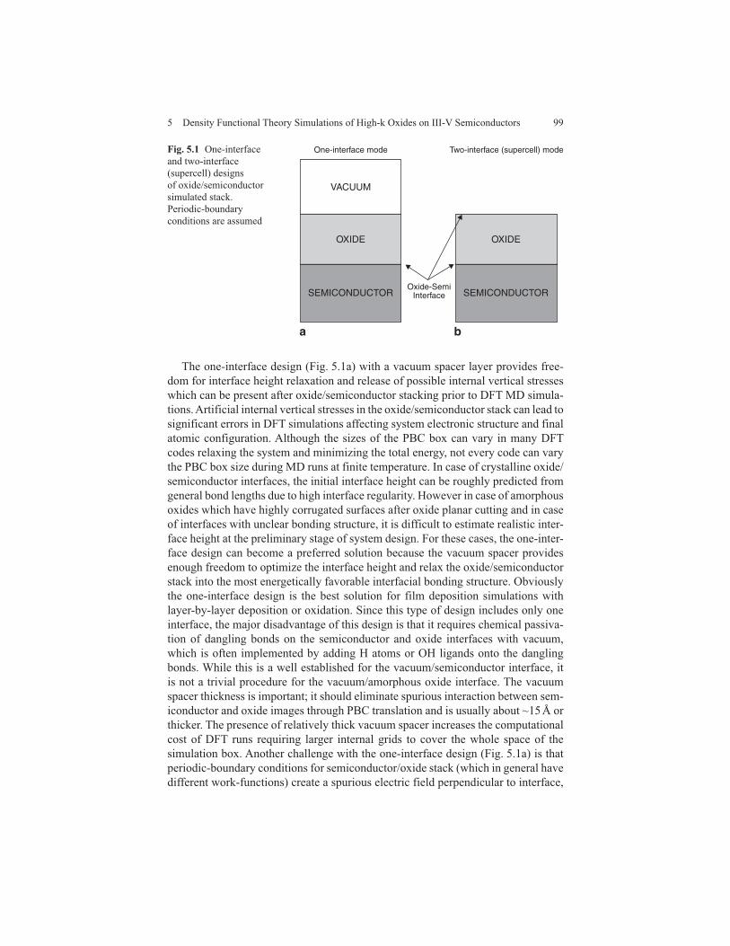
Another variation of oxide/semiconductor system simulations comes from differ-ent ways to arrange oxide and semiconductor slabs in periodic boundary condi-tion (PBC) box. Figure 5.1 presents two possible designs for oxide/semiconductor stack arrangement with periodic-boundary conditions. The design represented in Fig. 5.1a has only one oxide-semiconductor interface with a vacuum spacer above oxide; conversely design in Fig. 5.1 b has two oxide-semiconductor interfaces and no vacuum layer. Very often simulations incorporate interfacial layer between oxide and semiconductor which can be trivially incorporated into both Fig. 5.1 designs. Each of these two designs has its own advantages and disadvantages.
995 Density Functional Theory Simulations of High-k Oxides on III-V Semiconductors
The one-interface design (Fig. 5.1a ) with a vacuum spacer layer provides free-dom for interface height relaxation and release of possible internal vertical stresses which can be present after oxide/semiconductor stacking prior to DFT MD simula-tions. Artificial internal vertical stresses in the oxide/semiconductor stack can lead to significant errors in DFT simulations affecting system electronic structure and final atomic configuration. Although the sizes of the PBC box can vary in many DFT codes relaxing the system and minimizing the total energy, not every code can vary the PBC box size during MD runs at finite temperature. In case of crystalline oxide/semiconductor interfaces, the initial interface height can be roughly predicted from general bond lengths due to high interface regularity. However in case of amorphous oxides which have highly corrugated surfaces after oxide planar cutting and in case of interfaces with unclear bonding structure, it is difficult to estimate realistic inter-face height at the preliminary stage of system design. For these cases, the one-inter-face design can become a preferred solution because the vacuum spacer provides enough freedom to optimize the interface height and relax the oxide/semiconductor stack into the most energetically favorable interfacial bonding structure. Obviously the one-interface design is the best solution for film deposition simulations with layer-by-layer deposition or oxidation. Since this type of design includes only one interface, the major disadvantage of this design is that it requires chemical passiva-tion of dangling bonds on the semiconductor and oxide interfaces with vacuum, which is often implemented by adding H atoms or OH ligands onto the dangling bonds. While this is a well established for the vacuum/semiconductor interface, it is not a trivial procedure for the vacuum/amorphous oxide interface. The vacuum spacer thickness is important; it should eliminate spurious interaction between sem-iconductor and oxide images through PBC translation and is usually about ~15 Å or thicker. The presence of relatively thick vacuum spacer increases the computational cost of DFT runs requiring larger internal grids to cover the whole space of the simulation box. Another challenge with the one-interface design (Fig. 5.1a ) is that periodic-boundary conditions for semiconductor/oxide stack (which in general have different work-functions) create a spurious electric field perpendicular to interface,
Fig. 5.1 One-interface and two-interface (supercell) designs of oxide/semiconductor simulated stack. Periodic-boundary conditions are assumed
VACUUM
OXIDE
SEMICONDUCTOR
OXIDE
Oxide-SemiInterface
One-interface mode
a b
Two-interface (supercell) mode
SEMICONDUCTOR

100 E. A. Chagarov and A. C. Kummel
with the field mainly localized in the least-screened region (vacuum) and requiring compensation to avoid computational errors. Fortunately majority of modern DFT codes provides automatic correction/compensation of such artificial electric fields [ 52 – 54 ]. The one-interface design was successfully applied by Puthenkovilakam et al. for simulations of ZrO 2 /Si and ZrSiO 2 stacks [ 4 ], by Monaghan et al. for simula-tions of Hf silicates on Si [ 23 ], by Hakala et al. for simulations of HfO 2 on Si [ 24 ], by Gavartin et al. for simulations of HfO 2 /SiO 2 /Si stacks [ 26 ], by Chagarov et al. for simulations of a-Al 2 O 3 /Ge, a-ZrO 2 /Ge, a-Al 2 O 3 /InGaAs and a-Al 2 O 3 /InAlAs/InGaAs interfaces [ 36 , 37 , 49 , 50 ], and by other authors.
The two-interface (supercell) design (Fig. 5.1b ) has its own advantages and dis-advantages. It provides two oxide-semiconductor interfaces in one model with one additional interface coming from periodic-boundary condition translation. It has reduced computational cost due to absence of a vacuum spacer and a smaller system size. It also avoids the need to passive the vacuum/oxide interface and does not cre-ate artificial electric fields. However, its fixed structure in direction perpendicular to interface does not provide the system with enough freedom to release internal interfacial stresses which can form either during initial system design or during DFT MD annealing and/or relaxation. Although majority of DFT codes can vary the box size during relaxation, not all of them can not do it during DFT MD annealing. In case of unclear bonding structure in interface region and highly corrugated oxide and/or semiconductor surface (like in case of amorphous oxides), this type of design can lead to presence of significant stresses in the system distorting electronic struc-ture and final atomic geometry. However this type of design can be satisfactory in case of pre-determined bonding structure and previously well estimated interfacial bond-lengths. The two-interface (supercell) design was successfully used by Tse et al. for simulations of ZrO 2 /Ge interfaces [ 6 ], by Peacock et al. and by Ha et al. for simulations of ZrO 2 /Si and HfO 2 /Si stacks [ 16 , 27 ], by Broqvist et al. for modeling of HfO 2 /SiO 2 /Si and by other authors [ 11 , 32 , 33 ].
The different choice of the semiconductor/oxide stack design leads to different evaluation of some of its major properties. For example, for two-interface (super-cell) design (Fig. 5.1b ), the interface formation energy can be determined by:
Eform = Etot − (nEoxide + mEsemi + lμN )
2S, (5.4)
where E tot is a total energy of the relaxed system, n and E oxide are the number of oxide units and the total energy of such unit, m and E semi are the number of semicon-ductor units and the total energy of each unit, l and � N are the number of additional atomic species (like extra O or H for example) and their chemical potential, and S is an interface area. In case of one-interface design with vacuum spacer (Fig. 5.1a ), the Eq. (5.4) requires modification to take into account surface energies of passi-vated or unpassivated oxide and semiconductor surfaces.
The final choice of the oxide-semiconductor system design is determined by specific research goals, interface to be investigated, and the computational cost.

1015 Density Functional Theory Simulations of High-k Oxides on III-V Semiconductors
5.2.3 Crystalline vs. Amorphous Oxides in DFT Simulations
Experimentally, amorphous oxides for gate dielectrics are considered to be supe-rior to crystalline/polycrystalline ones since grain boundaries and dislocations in polycrystalline oxide films can lead to increased current leakage through the oxide. In addition, highly-ordered polycrystalline oxide/crystalline semiconductor inter-faces usually have lattice mismatch which results in a high density of dangling bonds acting as interfacial electrical defects. Some amorphous oxides, such as ZrO 2 and HfO 2 , can crystallize at relatively low temperatures ( < 500 ° C) [ 55 ]. Crystalline oxides tend to have higher dielectric constants so sometimes nanocrystalline materi-als are experimentally employed.
DFT simulations have different issues with modeling crystalline and amorphous oxide samples. Although for many perspective high-k oxide/semiconductor stacks such as HfO 2 /Si or ZrO 2 /Si, amorphous oxides are the most promising, there are many simulations of these stacks with crystalline oxides instead of amorphous ones [ 3 , 4 , 6 , 13 , 14 , 16 , 18 , 27 , 28 ]. The validity of approximation of amorphous oxides by crystalline systems in oxide/semiconductor stacks is not obvious; however, it has been very successful for simulating oxide defects [ 56 – 66 ].
One of the main reasons why crystalline oxide models are often used in DFT simulations of oxide/semiconductor stacks is that generation of realistic amorphous oxide models is a much more complicated task than building crystalline oxide sam-ples from well-known crystallographic information. The overview of techniques for computational generation of amorphous oxides will be provided later. The substi-tution of amorphous oxides in oxide/semiconductor DFT simulations by crystal-line systems can be problematic for modeling some interface properties. Crystalline oxide/semiconductor lattice mismatch can lead to artificial oxide compression/elon-gation in DFT models to match semiconductor area. Due to high computational cost of DFT runs, the typical atomic system size is usually limited to several hundred atoms thereby limiting the area of the oxide/semiconductor interface. The problem of lattice mismatch could be alleviated by employing larger interfacial areas and larger numbers of unit cells along the interfacial plane. However, this is not always feasible with typical computational resources. Since in DFT simulations both oxide and sem-iconductor share the same lateral sizes (parallel to the interface), the small interface area and lattice mismatch often require substantial oxide compression/elongation to match the semiconductor substrate area. This artificial oxide compression/elonga-tion can lead to sensible electronic structure distortions such as deformation of band structure, introduction of gap states, changing of band offsets and bond lengths [ 4 , 6 , 16 , 18 ]. The presence of vacuum spacer over the stack and system relaxation in vertical direction can provide only a partial reduction of these problems.
Another challenge of substituting amorphous oxides by crystalline ones comes from the enhanced risk of formation of partially filled dangling bonds in the inter-face region or distortion of substrate lattice positions during DFT-MD annealing. This can occur because of the lattice mismatch between the oxide and semiconduc-tor. The amorphous oxide surface with its atomic long-range disorder in contact with semiconductor has more homogeneous sampling of the ordered semiconductor

102 E. A. Chagarov and A. C. Kummel
surface patterns minimizing the risk of dangling form formation and substrate lat-tice distortion if the bonding between the amorphous oxide and semiconductor is weak. However, if the bonding is strong between the oxide and semiconductor, there will be dangling bond formation and substrate lattice distortion at the interface for both types of oxides.
Besides purely technical problems such as oxide-semiconductor lattice mis-match and dangling bond formation in interface region, substitution of amorphous high-k oxides in simulations of oxide/semiconductor interfaces by crystalline sys-tems changes some oxide properties particularly coordination numbers which in turn affects the band gap.
One of the major differences between the crystalline and amorphous high-k oxides comes from very different coordination distributions. Figure 5.2 presents atomic coordination distributions for crystalline Al 2 O 3 (corundum) and amorphous Al 2 O 3 generated by computer simulations [ 37 , 67 ]. It can be seen that the crystalline and amorphous Al 2 O 3 phases demonstrate very different coordination distributions. While crystalline Al 2 O 3 has 4-coordinated O and 6-coordinated Al with no coor-dination broadening, the coordination distribution for amorphous Al 2 O 3 introduces significant broadening, lowers Al coordination maximum to 4 and O coordination to 3 (Fig. 5.2 ). This comparison of coordination distributions for amorphous and crys-talline Al 2 O 3 samples (Fig. 5.2 ) indicates that despite chemical similarity, the amor-phous phase can have a different chemical environment of atoms which may affect some physical properties of the oxide. Momida et al. performed theoretical investi-gation of dielectric response of amorphous alumina and calculated that the difference in band gap between amorphous Al 2 O 3 in comparison with crystalline Al 2 O 3 was 2.8–3.9 eV (DFT value), which is in good correlation with the experimental band gap difference of 1.9–3.7 eV with the amorphous having a smaller bandgap than crystal-line oxide [ 68 – 70 ]. The more detailed theoretical research of Momida et al. indicated that the band-gap reduction in a-Al 2 O 3 was caused by the local potential changes on Al and O sites due to their lower coordination in comparison with crystalline poly-morphs correlating well with experimental measurements proposing roughly linear
Fig. 5.2 Coordination distribution for a amorphous Al 2 O 3 , b crystalline Al 2 O 3 (corundum) (Origi-nal figure used with permission of American Institute of Physics. E. Chagarov, A.C. Kummel, J. Chem. Phys. 130, 124717 (2009))
Par
titio
n (%
)
Par
titio
n (%
)
45
50
a b
Amorphous Al2O3
O Our SampleO by GutierrezAl Our SampleAl by Gutierrez
Crystalline Al2O3
40
35
30
25
20
15
10
5
01 2 3 4 5 6 1 2 3 4 5 6
100
90
80
70
60
50
40
30
20
10
0
OAl

1035 Density Functional Theory Simulations of High-k Oxides on III-V Semiconductors
relation between Al 2 O 3 bandgap and Al average atomic coordination [ 68 , 69 ]. Some amorphous oxides such as a-SiO 2 have the same coordination distribution as their crystalline polymorphs such as α -quartz due to their covalent bonding. However most high-k oxides such as a-Al 2 O 3 , a-ZrO 2 , a-HfO 2 have ionic bonding and their amorphous phases have different coordination distributions than crystalline poly-morphs, which can significantly affect physical properties such as band gaps.
5.2.4 The Oxide-Semiconductor Stack Simulation Techniques: DFT Relaxation vs. Molecular Dynamics
After high-k oxide is deposited on the semiconductor substrate (with or without an interfacial layer), there are two major computational approaches to simulate inter-face evolution to the final configuration: geometry optimization (relaxation) and molecular dynamics (annealing). Although there are other simulation techniques such as Monte-Carlo and hybrid MC-Molecular Dynamics approaches, the relaxa-tion and molecular dynamics annealing remain to be the most widely used compu-tational techniques for oxide/semiconductor interface research.
The goal of geometry optimization is to generate the lowest energy structure of an atomic system starting from an arbitrary initial configuration. Following the Born-Oppenheimer approximation, the motion of nuclei and electrons can be sepa-rated; therefore, geometry optimization typically includes a series of self-consistent single point energy calculations and adjustments of atomic positions. The forces on the nuclei can be calculated from the converged wavefunction using the Hellmann-Feynman theorem [ 71 ]:
FXγ= − ∂E
∂Xγ
= −⟨ψ
∣∣∣∣∣ ∂H
∂Xγ
∣∣∣∣∣ψ⟩
, (5.5)
where H –system Hamiltonian, � –system wavefunction, and � –parameter cor-responding to the coordinates of the nuclei. From the calculated forces acting on the atoms, the atomic coordinates are adjusted to minimize the system total energy by applying various relaxation algorithms. One of the most popular relaxation algo rithms is Broyden–Fletcher–Goldfarb–Shanno (BFGS) method developed for solving an unconstrained nonlinear optimization problem [ 72 , 73 ]. There are two sets of computational problems associated with geometry relaxation. The first set of problems includes Pulay force, which is an error introduced into the Hellman-Feynman forces if the basis set is incomplete, and a Pulay stress, which arises if the simulation cell shape changes during the simulation [ 74 , 75 ]. The second set of prob-lems results from the geometry optimization performed at zero kinetic (thermal) energy; this can lead to system relaxation into the closest configuration with zero forces, which can be a local, not the global minimum of the system. This feature makes geometry optimization very sensitive to the choice of initial configuration.

104 E. A. Chagarov and A. C. Kummel
The common approaches to avoid such problem is either to carefully choose initial configuration (this is not always possible) or to perform an initial energy minimiza-tion using molecular dynamics simulations at finite temperature to obtain the vicin-ity of the global minimum and then to perform a full geometry relaxation.
Molecular dynamics (MD) is a simulation technique, which in the most classical form is described by the following algorithm:
1. Choose the initial atomic positions R(0)i and choose a short timestep Δ t ;
2. Calculate the forces acting on atoms using certain forcefield (first-principle or empirical);
3. Evolve system in time moving atoms applying various integration algorithms, which approximate the expansion: R( j+1) = R( j) + V ( j)�t + 1
/2a �t2 + · · · 4. Update time: t = t +�t ;
5. Repeat steps (2)–(4) as long as necessary.
In case of DFT molecular dynamics simulations the forces in step (2) are often obtained by using the Hellmann-Feynman theorem (Eq. 5.5). There are various atom motion integration algorithms. The classical atom integration algorithms are Verlet and “leap-frog” (which is a modified version of Verlet algorithm) [ 76 – 80 ].
In Verlet algorithm, the atom positions are updated according to the following expression:
R(t +�t) = 2 ∗ R(t)− R(t −�t)+ a(t) ∗ �t2. (5.6)
The Verlet algorithm is straightforward, has modest memory demands, but moder-ate precision.
In the “leap-frog” algorithm, the atomic coordinate and velocities are updated according to different expressions:
R(t +�t) = R(t)+ v(t + 1
2�t) ∗ �t, (5.7)
v(t + 1
2�t) = v(t − 1
2�t)+ a(t) ∗ �t. (5.8)
In this algorithm, the velocities leap over the positions; afterwards, the positions leap over the velocities. In the leap-frog algorithm, the velocities are calculated explicitly, however, they are not calculated at the same time as atomic coordinates. In this case, the velocities at any moment of time t can be approximated by the fol-lowing relationship:
v(t) = 1
2∗[
v(t − 1
2�t)+ v(t + 1
2�t)
]. (5.9)
In modern classical MD simulations, old atom integration algorithms such as Ver-let or “leap-frog” are often substituted by more sophisticated and more efficient

1055 Density Functional Theory Simulations of High-k Oxides on III-V Semiconductors
algorithms such as r-RESPA, which implements a multi-timestep scheme applied differently to integration of short- and long-range interactions in the system provid-ing significant boost to the computational efficiency [ 81 – 83 ].
The timestep in molecular dynamics simulations is chosen to provide satisfac-tory accuracy of atom motion integration and energy conservation in an adiabatic ensemble. If the timestep is too long, the violation of energy conservation becomes very severe. A typical timestep for molecular dynamics simulations is about 1 fs = 1.0 × 10 �15 (s). However in case of very high temperatures or the presence of very light elements such as H, the timestep of MD simulations is often reduced to 0.1–0.5 fs to maintain proper level of energy conservation and integration accuracy. The relatively short typical timestep of ~1 fs and significant computational cost of DFT calculations for one atomic configuration limit the typical simulated time-span for DFT MD simulations to ~1–100 ps.
One of the major differences between geometry relaxation and molecular dynamic simulations is that many algorithms for geometry relaxation, such as BFGS or Conjugate Gradient (CG), are not bound to a real time frame and include only artificial atom movements, while the molecular dynamics and its system evolution are always logically connected to the real time frame. Another major difference is that many relaxation techniques, such as BFGS or Conjugate-Gradient, imply zero temperature (zero thermal energy) of the system and have an internal propensity to converge to the local minima. Conversely, molecular dynamics simulations are generally performed at finite temperature, which allows the system to pass over modest energy barriers and evolve to the global minimum. MD simulation can be performed as a function of temperature and annealing time to optimize the evo-lution to the global minimum. In general, finite-temperature molecular dynamics simulations of the oxide/semiconductor interfaces are finalized by cooling-relaxa-tion or relaxation to converge to the ground state atomic configuration. Contrary to relaxation by GC and BFGS, DFT MD simulations can be performed as a function of temperature and annealing time to analyze system behavior. Although molecular dynamics simulations can be performed for different numbers of timesteps (sim-ulated time span), in general, DFT geometry relaxations of oxide/semiconductor interfaces are computationally cheaper while DFT MD runs are generally much more computationally expensive.
The geometry relaxation and molecular dynamics approaches have been used for multiple simulations of high-k oxide/semiconductor interfaces. Peacock et al., Tse et al., Robertson et al., and Xiong et al. successfully applied DFT geometry relaxation approach to the investigation of ZrO 2 /Si, HfO 2 /Si, and ZrO 2 /Ge inter-faces [ 6 , 13 – 16 ]. Giorgi et al., Kawamoto et al., Puthenkovilakam et al., Dong et al., and Zhang et al. applied geometry relaxation to the investigation of SrTiO 3 /Si, ZrO 2 /Si, HfO 2 /Si, ZrSiO 4 /Si, and HfSiO 4 interfaces [ 4 , 5 , 18 , 20 , 28 ]. In these cases, geometry relaxation was preferred over molecular dynamics since initial interfaces in these studies were designed to have very specific configurations; molecular dynamics with its kinetics at finite temperature would bring significant chaos to the atomic configurations. Broqvist et al. and Ha et al. successfully applied geometry relaxation to the investigation of defects in HfO 2 /Si and a-HfO 2 /Si systems creating defects and relaxing the interfaces [ 11 , 27 ].

106 E. A. Chagarov and A. C. Kummel
Although geometry relaxation can be a preferred technique when interface con-figuration is roughly known a priori, in situations when the oxide/semiconductor interface configuration is not known, molecular dynamics at finite temperature becomes a preferred technique since it can sample many atomic configurations both in local and global minima. Monaghan et al., Hakala et al., Gavartin et al., Broqvist et al., and Chagarov et al. successfully applied DFT molecular dynamics simula-tions to the investigation of HfSiO 4 /Si, HfO 2 /Si, HfO 2 /SiO 2 /Si, a-HfO 2 /SiO 2 /Si, a-Al 2 O 3 /Ge, a-ZrO 2 /Ge, a-Al 2 O 3 /InGaAs and a-Al 2 O 3 /InAlAs/InGaAs interfaces [ 23 , 24 , 26 , 32 , 33 , 36 , 37 , 49 , 50 ].
The geometry relaxation and molecular dynamics techniques have their own advantages and disadvantages; therefore, the final choice of technique is usually dictated by specifics of the research goals and affordable computational cost.
5.3 DFT Simulations of High-k Oxides on Si/Ge Substrates
Although DFT simulations of high-k/III-V semiconductor stacks are different from simulations of high-k/Si or high-k/Ge interfaces, they can naturally inherit many useful methodological and research solutions previously developed and successfully employed for investigation of high-k/Si stacks. This chapter will provide overview of some DFT approaches and results on high-k/Si and high-k/Ge systems useful for modeling of the next generations of high-k/III-V oxide-semiconductor interfaces.
The main reason high-k oxides have become a necessity in commercialMOSFETs is that the scaling of the traditional SiO 2 oxide below 7–13 Å is fundamen-tally impossible due to the direct tunneling through the oxide [ 1 , 2 ]. Furthermore, at oxides thickness of only a few atomic monolayers, the oxide properties begin to significantly deviate from the traditional bulk values. This problem is important even for high-k/Si devices because ultra-thin a-SiO 2 layers are often spontaneously formed between high-k dielectrics and Si substrates [ 84 ]. Although the dielectric constant of the bulk a-SiO 2 oxide ( ε 0 = 3.9) is often used for estimations of the oxide electrical properties in the a-SiO 2 /semiconductor stacks, there are significant concerns about validity of this assumption since experimental measurements report unusual electronic and structural properties for the first few angstroms of SiO 2 such as reduced band-gap and higher dielectric constant values [ 2 , 84 , 85 ].
To clarify this effect, Giustino et al. performed DFT simulations of Si-SiO 2 stacks varying the SiO 2 thickness from 0 to 20 Å and calculating the static ( ε 0 ) and high-frequency ( ε � ) dielectric constants for the ultra-thin SiO 2 layers as a function of the film thickness [ 25 ]. The oxide was modeled by �-cristobalite using two inter-face models with various ratios of silicon to oxygen with all the oxygen in an O �2 state. In model I, the interfacial layer was formed by 1 ML of Si +1 and 1/2 ML of Si +2 [ 25 , 86 ]. In model II, the interfacial layer was formed by equal amounts with 1/2 ML of Si +1 , Si +2 , and Si +3 atoms [ 25 , 87 , 88 ]. The static and high-frequency per-mittivities were calculated by the standard Berry-phase approach [ 89 ]. As shown in Fig. 5.3 , the static and high-frequency dielectric permittivities of SiO 2 increase as the oxide thickness decreases, indicating significant deviation from the bulk-type
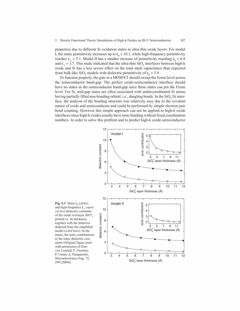
1075 Density Functional Theory Simulations of High-k Oxides on III-V Semiconductors
properties due to different Si oxidation states in ultra-thin oxide layers. For model I, the static permittivity increases up to ε 0 = 10.1, while high-frequency permittivity reaches ε � = 5.1. Model II has a smaller increase of permittivity reaching ε 0 = 6.8 and ε � = 3.7. This study indicated that the ultra-thin SiO 2 interlayer between high-k oxide and Si has a less severe effect on the total stack capacitance than expected from bulk-like SiO 2 models with dielectric permittivity of ε 0 = 3.9.
To function properly, the gate in a MOSFET should sweep the Fermi level across the semiconductor band-gap. The perfect oxide-semiconductor interface should have no states in the semiconductor band-gap since these states can pin the Fermi level. For Si, mid-gap states are often associated with undercoordinated Si atoms having partially filled non-bonding orbital, i.e., dangling bonds. In the SiO 2 /Si inter-face, the analysis of the bonding structure was relatively easy due to the covalent nature of oxide and semiconductor and could be performed by simple electron-pair bond counting. However this simple approach can not be applied to high-k oxide interfaces since high-k oxides usually have ionic bonding without fixed coordination numbers. In order to solve this problem and to predict high-k oxide-semiconductor
Fig. 5.3 Static ε 0 ( disks ) and high-frequency ε � ( open circles ) dielectric constants of the oxide overlayer SiO* 2 plotted vs. its thickness, together with the behavior deduced from the simplified model ( solid lines ). In the insets, the ionic contributions to the static dielectric con-stants (Original figure used with permission of Else-vier Limited. F. Giustino, P. Umari, A. Pasquarello, Microelectronics Eng. 72, 299 (2004))
3 4 5
SiO2* layer thickness (Å)
SiO2* layer thickness (Å)
3
3
25
5
4
7 9 11
6 7 8 9 10 11 12
12
10
8
6
4
2
diel
ectr
ic c
onst
ant
ioni
c co
ntrib
utio
nmodel II
12
10
8
6
4
23 4 5
SiO2* layer thickness (Å)
6 7 8 9 10 11 12
diel
ectr
ic c
onst
ant
SiO2* layer thickness (Å)
3
3
25
5
4
7 9 11
ioni
c co
ntrib
utio
nmodel I

108 E. A. Chagarov and A. C. Kummel
insulating interfaces, Peacock et al. formulated the following electron counting rules for ionic oxide/covalent semiconductor substrate interfaces [ 13 ]:
1. terminate with faces with enough excess oxygen so that the interfacial Si dan-gling bonds (DBs) are formally Si+ and empty, or
2. terminate with excess metal so the Si DBs are formally Si− and filled.
These rules are quite general and can be applied to the bonding between high-k (crystalline or amorphous) oxide and III-V semiconductors.
To test and verify these set of electron counting rules, Peacock et al. performed set of DFT relaxation calculations for various O- and Zr-terminated ZrO 2 /Si inter-faces (Fig. 5.4 ) [ 13 ]. The O 4V configuration (Fig. 5.4 a ) has fourfold coordinated interfacial O atoms and leaves the Si dangling bonds to be half-filled predicting the interface to be metallic in full agreement with DFT calculations. The interface in Fig. 5.4 b (O 4 ) in its initial state has twice as many interfacial oxygens with sixfold Si’s and fourfold O’s. After relaxation to the configuration presented in Fig. 5.4 c with fourfold interfacial Si’s, it is predicted to be an insulating interface confirmed by DFT calculations; by insulating Peacock et al. imply the valence and conduc-tion bands are well separated with no midgap states, and, therefore consistent with unpinning. The third type of interface (named O 3 ) is presented in Fig. 5.4d and relaxes to the state with fivefold coordinated interfacial Si atoms, while half the interfacial O atoms bond to two Si’s and one Zr, and the other half bonds to two Zr’s and one Si atom. According to the proposed electron counting rules, this interface
Fig. 5.4 Atomic configurations of various unrelaxed [( b ) only] and relaxed Si:ZrO 2 interfaces, viewed in the (110) plane (Original figure used with permission of American Physical Society. P.W. Peacock and J. Robertson, Phys. Rev. Lett. 92, 057601 (2004))

1095 Density Functional Theory Simulations of High-k Oxides on III-V Semiconductors
should be insulating in complete agreement with DFT calculations [ 13 ]. The last O-terminated interface among investigated is presented in Fig. 5.4e (named O 3B ). For this configuration one of the Si dangling bonds is accommodated in the Si–O–Si bridge, while the second dangling bond is bonded to the OZrO unit. However since OZrO unit has a closed shell, Si dangling bond needs an extra O half-monolayer to donate an electron resulting in configuration Si + (O 2� ) 0.5 OZrO. The formulated elec-tron counting rules predict this interface to be insulating in complete agreement with performed DFT calculations. The O 3 , O 3B , and O 4 interfaces have the same number of O atoms, and the O 3 interface (Fig. 5.4d ) is the most stable configuration.
One of the possible Zr-terminated interfaces (Zr 6 ) is presented in Fig. 5.4g . In this interface, there are two Zr–Si bonds per interfacial Si, and Zr is in the Zr +4 state satisfying bonding rules and predicting the interface to be insulating. The DFT simulations show a band-gap in agreement with the prediction; however, there are gap states (i.e., pinned) due to the Zr electronegativity, which makes this interface not usable for microelectronics applications. The second Zr-terminated interface (Zr 10 ) is presented in Fig. 5.4h and has tenfold coordinated Zr atoms. According to the electron counting rules, this interface should be insulating, however DFT simu-lations find it to be metallic (i.e., pinned) due to the high Zr coordination number causing band overlap. In addition Peacock et al. investigated O 4V structure with half-monolayer of Zr substituted for Si in the interfacial layer (Fig. 5.4f ) as sug-gested by Fiorentini et al. and found it to be metallic consistent with the electron counting rules [ 13 , 19 ]. The two Zr-terminated interfaces (Zr 6 and Zr 10 ) emphasize the general validity of the electron counting predictions while demonstrating that they can be violated by the electron structure nuances of the particular oxide/semi-conductor stacks. Nevertheless, the formulated electron counting rules proved to be valuable tool for predicting the high-k oxide/semiconductor stack properties and can be extrapolated to the amorphous high-k oxides and III-V semiconductors [ 32 ].
When applying the electron counting rules, two technical aspects should be taken into account: first, engineering of the initial interface to satisfy these rules does not guarantee that the final ground state bonding configuration will be insulating since geometry relaxation can distort the interface geometry resulting in unsatisfied bonding rules and a metallic interfacial electronic structure; secondly, the geometry relaxation of the manually designed interfaces performed at zero temperature have a significant propensity to converge to the local (not global) minima; this problem can be solved by applying molecular dynamics simulations at finite temperature capable of sampling many interface configurations and predicting the most energetically favorable one.
Another important aspect of high-k/Si DFT simulation heritage that is useful for future modeling of high-k/III-V stacks is a modeling of defects in high-k oxides. The problem of defects (vacancies or interstitials) in high-k dielectrics and their passivation has tremendous technological importance, since unpassivated defects can create pinning states in the bandgap region having detrimental effect on the total device performance. The DFT with its microscopic, atomistic approach can provide detailed insight into the major aspects of the defect problem in high-k oxides such as energy levels in the bandgap, formation energies, defect migration energy barri-ers and their passivation [ 11 , 12 , 26 , 27 , 32 – 35 , 56 , 90 – 93 ].

110 E. A. Chagarov and A. C. Kummel
The defect formation energy in a charge state q can be expressed via the electron chemical potential � referred to the valence band maximum ε � [ 94 ]:
Eqf (μ) = Eq
tot − Ebulktot −
∑α
nαηα + q(μ+ ευ), (5.10)
where Eqtot is a total energy of the defect system, Ebulk
tot the total energy of the unperturbed system, nα the number of extra atoms of species � needed to create the defect, and ηα the corresponding atomic chemical potential.
The defects can demonstrate different properties in crystalline and amorphous polymorphs of high-k oxides. Broqvist et al., and Capron et al. performed compre-hensive studies of oxygen vacancies in crystalline, amorphous HfO 2 systems and a-HfO 2 /SiO 2 /Si interfaces [ 11 , 32 – 34 ]. These studies provided comparison between defect properties in crystalline and amorphous high-k oxides. In addition, defect tracking in an amorphous system with its more disordered network becomes a non-trivial issue, which makes these studies interesting from methodological point of view. For monoclinic HfO 2 , the formation energies for three- and fourfold coordi-nated neutral oxygen vacancies are 9.1 eV and 8.9 eV (endothermic) respectively agreeing well with the previously published data [ 11 ]. Besides coordination, the vacancy formation energy depends on vacancy charge state. For monoclinic HfO 2 , the threefold oxygen vacancy in positively charged states (+1 and +2) has a lower energy, while fourfold oxygen vacancy is a more favorable for the neutral and nega-tively charged states (�1 and �2) [ 11 ]. For amorphous HfO 2 , the reported DFT-cal-culated vacancy formation energy has an average value of 8.85 eV (with standard deviation of 0.29 eV), which is lower than for the monoclinic phase [ 11 ]. The DFT MD annealing at 2000 K demonstrated the stability of the neutral oxygen vacancy in amorphous HfO 2 network and stability of its formation energy. However the DFT MD annealing of the doubly-positively charged vacancy V 2+ in a-HfO 2 dem-onstrated different behavior with the formation energy decreasing by 2.6 eV making the system more stable [ 11 ].
The defect energy levels and their location relative to the band gap are very important for technological applications to avoid pinning states. For monoclinic HfO 2 , the energy levels of the neutral (V 0 ) and doubly-positively charged vacancies (V 2+ ) for three- and fourfold coordinations were calculated; the neutral vacancies created occupied states in the middle of the HfO 2 band gap, while the V 2+ vacancies created states in the band gap closer to the conduction band [ 11 ]. The energy level for the three-coordinated oxygen vacancy is closer to the conduction band than the four-coordinated vacancy by ~0.2 eV for the neutral vacancy and by ~0.3 eV for the V2+ charged vacancy. The vacancy energy levels in amorphous HfO 2 demonstrate certain similarity in comparison with the monoclinic phase: the neutral vacancy V 0 levels are located in the band gap middle (2.7 eV from the valence band), while V 2+ vacancy levels are a little closer to the conduction band than the corresponding levels in the monoclinic phase. After DFT MD annealing of the amorphous HfO 2 , the energy levels of the neutral V 0 and charged V 2+ vacancies shift to the conduction band with V 2+ level getting very close to the conduction band edge [ 11 ]. Although

1115 Density Functional Theory Simulations of High-k Oxides on III-V Semiconductors
the annealing shifts these levels towards the conduction band, they still remain in the band gap thereby pinning it.
In the high-k oxide/semiconductor stacks, the vacancies can have different for-mation energies in different parts of the stack indicating propensity for vacancy migration in heterojunctions. To investigate this effect, Broqvist et al. modeled the HfO 2 /SiO 2 /Si stack calculating the formation energies for the oxygen vacancy in the middle of the a-HfO 2 layer vs. the vacancy in the a-HfO 2 /SiO 2 interfacial region [ 11 ]. While the vacancy in the middle of the a-HfO 2 layer had a formation energy (9.3 eV) close to the in-bulk a-HfO 2 value, the vacancy in the a-HfO 2 /SiO 2 interface had for-mation energy of 8.1 eV, or by 1.2 eV lower than the in-bulk value clearly indicating the oxygen vacancy propensity to migrate from the a-HfO 2 bulk to the a-HfO 2 /SiO 2 interface which was reported in previous theoretical studies [ 24 , 95 ]. However, the computational propensity for vacancy migration is insufficient to insure experimental diffusion at finite temperature and should be complemented by the energy barriers low enough to be overcome at typical processing temperatures. Capron et al. per-formed DFT simulations of oxygen vacancy migration in neutral V 0 and charged V 2+ states in monoclinic HfO 2 and through HfO 2 /SiO 2 interface reporting that in mono-clinic HfO 2 the activation barriers for the long-range diffusion are 2.4 eV and 0.7 eV for the neutral V 0 and charged V 2+ vacancies respectively [ 34 ]. These DFT predic-tions of the vacancy thermodynamic driving force towards the SiO 2 interface and low V 2+ vacancy migration barriers are in good agreement with reported experimental measurements [ 96 – 99 ].
The fact that defects in high-k oxides or their interfaces with semiconductors can form pinning states in the band gap region logically leads to the necessity of interface passivation to reduce pinning states. Ha et al. performed DFT simulations of HfO 2 /SiO 2 interface suggesting several possible mechanisms of the interface passivation [ 27 ]. In these modeling studies, the interface was formed by crystal-line (cubic) HfO 2 and crystalline SiO 2 (low-cristobalite). Although the ideal abrupt HfO 2 /SiO 2 interface was simulated, the density of states revealed pinning states coming from under-coordinated interfacial Hf atoms. In the bulk, Hf has at least 7 oxygen neighbors, while in the simulated interface, Hf was bonded only to 5 or 6 oxygen atoms. As a result, nonbonding Hf d-orbital produced pinning state in the band gap. The similar oxygen under-coordination problem was found by Kralik et al. for ZrO 2 [ 100 ]. Ha et al. investigated usage of O interstitials to passivate Hf under-coordinated defects [ 27 ]. The DFT calculations indicate that O has a binding energy about 2 eV more favorable to segregate at the interface rather than to stabilize inside HfO 2 or SiO 2 regions [ 27 ]. When O interstitials are included into the interface region, they bind Hf nonbinding states, restore Hf normal coordination, and remove pinning states from the band gap. However, for practical applications, this method is not very useful since high concentration of oxygen will lead to Si subsurface oxi-dation decreasing gate capacitance and deteriorating stack properties. The chlorine (Cl) was investigated among other possible passivation chemicals [ 27 ]. Chlorine has a useful propensity to segregate in HfO 2 /SiO 2 interface region where its binding energy is ~4 eV higher than in HfO 2 bulk [ 27 ]. While oxygen can accommodate two nonbonding electrons, Cl can accommodate just one electron of under-coordinated
112 E. A. Chagarov and A. C. Kummel
interfacial Hf. Similar to oxygen passivation, passivation by Cl requires very well controlled Cl dosing because excessive amounts of Cl will remain as interstitials defects, trapping electrons, and producing negative fixed charge. The oxygen and chlorine are not the only possible passivants. For a long time H has been used for passivation of defects in Si-based devices and has been a focus of active research [ 101 – 132 ].
5.4 Generation of Amorphous High-k Oxide Samples by Hybrid Classical-DFT Molecular Dynamics Computer Simulations
Experimentally, amorphous high-k oxide/semiconductor interfaces are expected to be superior to crystalline oxide-semiconductor counterparts due to the lack of lat-tice mismatch at amorphous oxide-semiconductor interfaces that can induce a high density of interface defects and the absence of grain-boundaries that can act as cur-rent leakage pathways. Despite their chemical composition similarity to crystalline polymorphs, amorphous high-k oxides demonstrate quite different microstructures, coordination distributions, and atomistic chemical environments.
The generation of realistic amorphous oxide samples is a non-trivial research task since contrary to crystalline samples, amorphous oxides do not have well-defined atomic structure. In case of high-k oxides, this problem is particularly challeng-ing since, unlike covalent oxides, the high-k oxides very often have ionic bonding which gives broad coordination distributions. The one of the most robust compu-tational techniques for generation of amorphous samples is a hybrid classical-DFT molecular dynamics “melt-and-quench” approach, which found many applications in generation of amorphous high-k oxides [ 11 , 33 , 36 – 38 , 133 – 144 ]. This hybrid approach starts with classical molecular dynamics annealing after which the sam-ple is transferred to DFT code and annealed for some additional time in the DFT forcefield. Sometimes sample transfer from classical to DFT code includes sample volume rescaling to reflect small difference of the sample density in the classical and DFT forcefields [ 36 – 38 ]. Usually the classical molecular dynamics has lower accuracy than DFT simulations, but classical MD is much more computationally efficient and can simulate much longer timescales than DFT MD. Conversely, DFT MD has higher accuracy (especially for irregular atomic systems as amorphous samples), but is much more computationally expensive and has limited affordable simulated timescales. The hybrid classical-DFT MD technique tries to combine the best features of the classical and DFT MD approaches. Figure 5.5 presents two possible hybrid classical-DFT MD approaches successfully applied to atomistic generation of realistic high-k oxides such as a-Al 2 O 3 , a-ZrO 2 , and a-HfO 2 [ 11 , 33 , 36 – 38 , 142 – 144 ].
The first sequence (Fig. 5.5a ) starts from ordered system at artificially low clas-sical density (such as ρ norm / ρ low ~ 3.38 [ 36 – 38 ]); annealing with classical MD at

1135 Density Functional Theory Simulations of High-k Oxides on III-V Semiconductors
very high temperature (high-T) for a long time results in significant system inter-mixing which erases the original ordered geometry. Afterwards, the high-T melt is instantaneously rescaled from low to normal density, annealed at high temperature for an additional period of time to equilibrate it at the new normal classical density, and linearly cooled from high to room temperature (RT) passing through the amor-phization stage. The cooled sample is equilibrated at RT finalizing the classical MD stage. Due to low computational cost, classical amorphous samples can be produced in batches varying annealing time and/or temperatures and choosing the most real-istic sample [ 36 – 38 , 145 ].
Published studies show that the classical molecular dynamics simulations with accurate interatomic potentials alone are able to produce amorphous high-k samples such as a-Al 2 O 3 [ 133 – 138 ]. However, since DFT force-field generally provides a more accurate interaction model than empirical interatomic potentials of classical MD, the sequence in Fig. 5.5a introduces further sample refinement by performing subsequent DFT annealing, cooling, and relaxation to tune the sample to the more accurate DFT force-field. To bridge between classical and DFT MD, the selected
Fig. 5.5 Hybrid classical-DFT molecular dynamics generation of amorphous oxide samples
Temp
Time
Low-ρ oxide Density Rescaling(low ρ→normal ρ)
High-T annealat low-ρ
High-T annealat normal-ρ
Coolingto RT
Equilibrationat RT
Coolingto 0K
Relaxation
Anneal belowmelting T
Density Rescaleclassical →DFT
Classical MD DFT MD
Time
Low-ρ oxide Density Rescaling(low ρ→normal ρ)
High-T annealat low-ρ
High-T annealat normal-ρ
Coolingto ~1000K
Density RescaleClassical →DFT
Classical MD DFT MD
Relaxation
Temp
a
b
114 E. A. Chagarov and A. C. Kummel
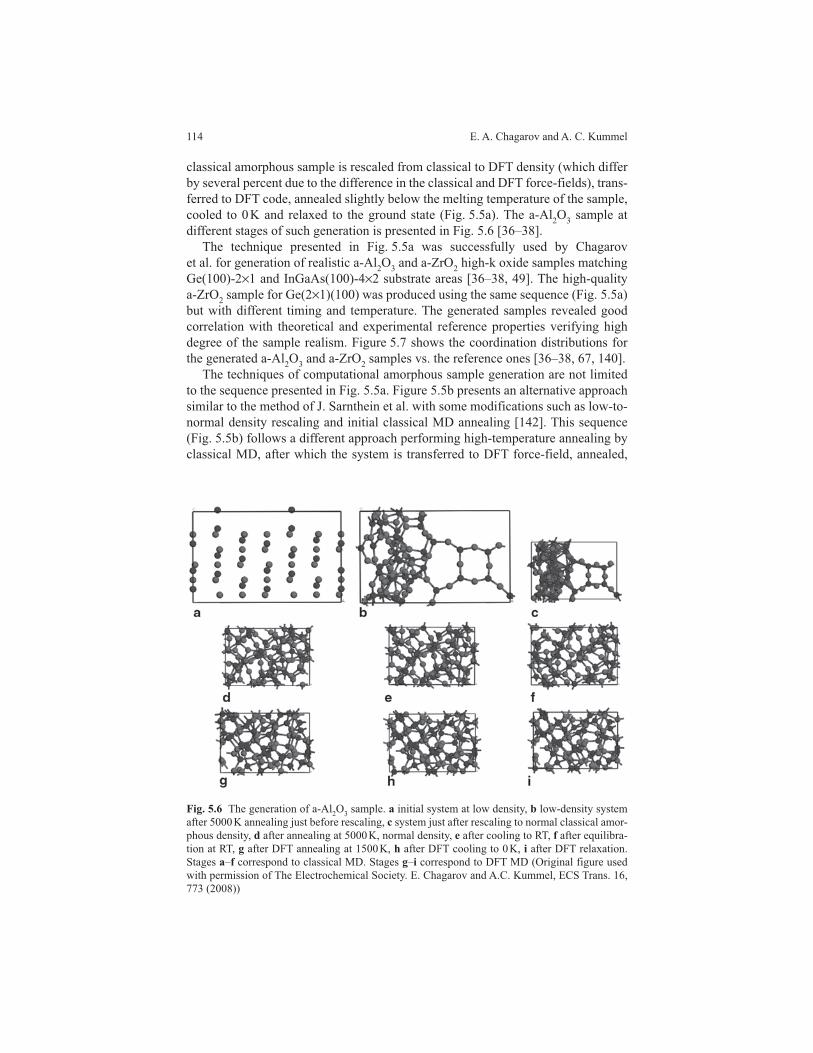
classical amorphous sample is rescaled from classical to DFT density (which differ by several percent due to the difference in the classical and DFT force-fields), trans-ferred to DFT code, annealed slightly below the melting temperature of the sample, cooled to 0 K and relaxed to the ground state (Fig. 5.5a ). The a-Al 2 O 3 sample at different stages of such generation is presented in Fig. 5.6 [ 36 – 38 ].
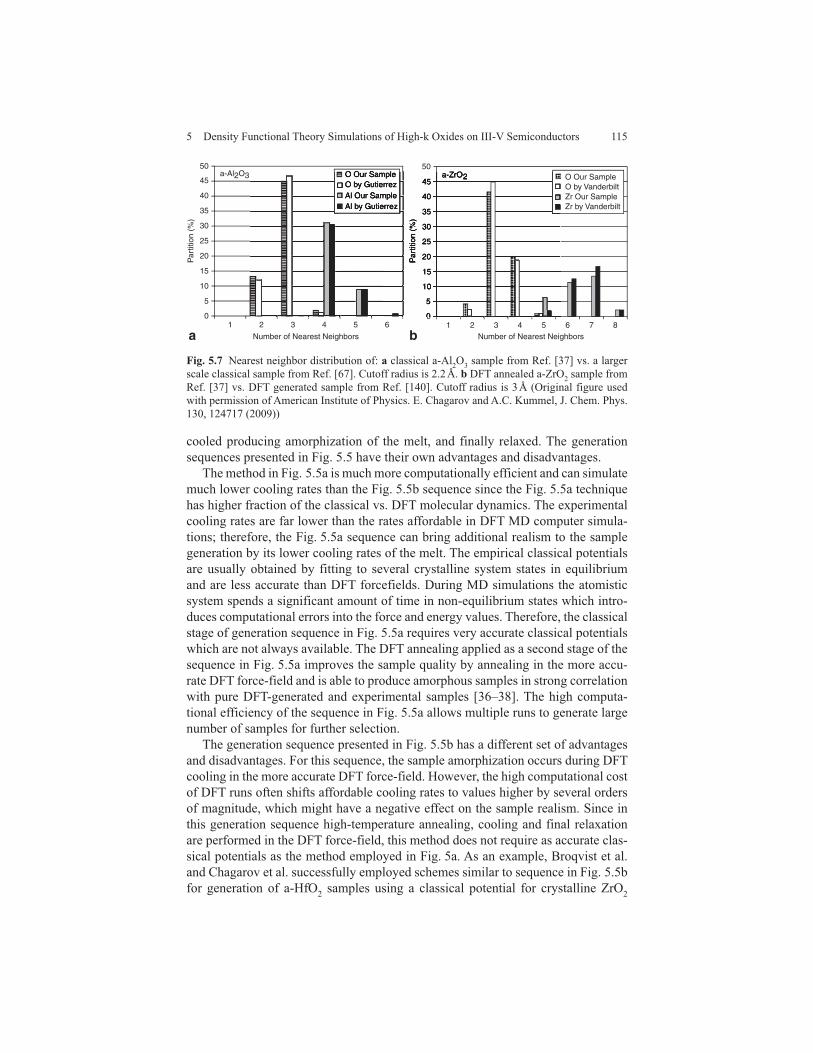
The technique presented in Fig. 5.5a was successfully used by Chagarov et al. for generation of realistic a-Al 2 O 3 and a-ZrO 2 high-k oxide samples matching Ge(100)-2 × 1 and InGaAs(100)-4 × 2 substrate areas [ 36 – 38 , 49 ]. The high-quality a-ZrO 2 sample for Ge(2 × 1)(100) was produced using the same sequence (Fig. 5.5a ) but with different timing and temperature. The generated samples revealed good correlation with theoretical and experimental reference properties verifying high degree of the sample realism. Figure 5.7 shows the coordination distributions for the generated a-Al 2 O 3 and a-ZrO 2 samples vs. the reference ones [ 36 – 38 , 67 , 140 ].
The techniques of computational amorphous sample generation are not limited to the sequence presented in Fig. 5.5a . Figure 5.5b presents an alternative approach similar to the method of J. Sarnthein et al. with some modifications such as low-to-normal density rescaling and initial classical MD annealing [ 142 ]. This sequence (Fig. 5.5b ) follows a different approach performing high-temperature annealing by classical MD, after which the system is transferred to DFT force-field, annealed,
Fig. 5.6 The generation of a-Al 2 O 3 sample. a initial system at low density, b low-density system after 5000 K annealing just before rescaling, c system just after rescaling to normal classical amor-phous density, d after annealing at 5000 K, normal density, e after cooling to RT, f after equilibra-tion at RT, g after DFT annealing at 1500 K, h after DFT cooling to 0 K, i after DFT relaxation. Stages a – f correspond to classical MD. Stages g – i correspond to DFT MD (Original figure used with permission of The Electrochemical Society. E. Chagarov and A.C. Kummel, ECS Trans. 16, 773 (2008))
1155 Density Functional Theory Simulations of High-k Oxides on III-V Semiconductors
cooled producing amorphization of the melt, and finally relaxed. The generation sequences presented in Fig. 5.5 have their own advantages and disadvantages.
The method in Fig. 5.5a is much more computationally efficient and can simulate much lower cooling rates than the Fig. 5.5b sequence since the Fig. 5.5a technique has higher fraction of the classical vs. DFT molecular dynamics. The experimental cooling rates are far lower than the rates affordable in DFT MD computer simula-tions; therefore, the Fig. 5.5a sequence can bring additional realism to the sample generation by its lower cooling rates of the melt. The empirical classical potentials are usually obtained by fitting to several crystalline system states in equilibrium and are less accurate than DFT forcefields. During MD simulations the atomistic system spends a significant amount of time in non-equilibrium states which intro-duces computational errors into the force and energy values. Therefore, the classical stage of generation sequence in Fig. 5.5a requires very accurate classical potentials which are not always available. The DFT annealing applied as a second stage of the sequence in Fig. 5.5a improves the sample quality by annealing in the more accu-rate DFT force-field and is able to produce amorphous samples in strong correlation with pure DFT-generated and experimental samples [ 36 – 38 ]. The high computa-tional efficiency of the sequence in Fig. 5.5a allows multiple runs to generate large number of samples for further selection.
The generation sequence presented in Fig. 5.5b has a different set of advantages and disadvantages. For this sequence, the sample amorphization occurs during DFT cooling in the more accurate DFT force-field. However, the high computational cost of DFT runs often shifts affordable cooling rates to values higher by several orders of magnitude, which might have a negative effect on the sample realism. Since in this generation sequence high-temperature annealing, cooling and final relaxation are performed in the DFT force-field, this method does not require as accurate clas-sical potentials as the method employed in Fig. 5a . As an example, Broqvist et al. and Chagarov et al. successfully employed schemes similar to sequence in Fig. 5.5b for generation of a-HfO 2 samples using a classical potential for crystalline ZrO 2
Fig. 5.7 Nearest neighbor distribution of: a classical a-Al 2 O 3 sample from Ref. [ 37 ] vs. a larger scale classical sample from Ref. [ 67 ]. Cutoff radius is 2.2 Å. b DFT annealed a-ZrO 2 sample from Ref. [ 37 ] vs. DFT generated sample from Ref. [ 140 ]. Cutoff radius is 3 Å (Original figure used with permission of American Institute of Physics. E. Chagarov and A.C. Kummel, J. Chem. Phys. 130, 124717 (2009))
Par
titio
n (%
)45
50
a b
O Our Samplea-Al2O3O by GutierrezAl Our SampleAl by Gutierrez
O Our SampleO by VanderbiltZr Our SampleZr by Vanderbilt
40
35
30
25
20
15
10
5
01 2 3 4 5 6
Par
titio
n (%
)
45
50a-ZrO2
40
35
30
25
20
15
10
5
0
Number of Nearest NeighborsNumber of Nearest Neighbors1 2 3 4 5 6 7 8

116 E. A. Chagarov and A. C. Kummel
[ 11 , 50 ]. The main disadvantage of the scheme in Fig. 5.5b is the high computational cost, which limits achievable simulation timescale as well as the number of prepared samples; having just few prepared samples restricts subsequent selection of the most realistic one.
The two amorphous sample generation sequences presented in Fig. 5.5 do not cover all possible amorphous sample generation solutions and can be significantly modified depending on particular simulation goals. For modern computational facilities, there is no universal solution for amorphous sample generation, and there is no universal recipe for selection the best method. In each particular case, the choice of amorphous sample generation procedure is dictated by particular system properties, required accuracy and affordable computational efficiency.
The computational generation of amorphous oxide samples requires elaborate tests to verify the quality of the samples. The choice of particular sample tests depends on the available reference properties and may be based upon both experi-mental and simulated data. Among the most frequently used sample quality tests are the calculations of radial-distribution functions (RDF), angular-distribution func-tions (ADF), coordination distributions, average coordination numbers, neutron scattering static structure factors and their comparison to the reference data.
The radial-distribution function (RDF) for atomic pair � - � is calculated accord-ing to Eq. (5.11), where nα,β(r, r +�r) is a number of � atoms within cutoff radius/shell (r, r +�r) from � -type atom, ρβ = Nβ/V is the number density of atoms � , and N � is the total number of � atoms. To make the RDF curves smoother, they are often calculated for a series of atomic configurations spanned by certain time inter-val (e.g., 10 fs), and finally averaged to minimize statistical noise. The typical RDF curves for classically generated a-Al 2 O 3 sample are presented in Fig. 5.8 .
gαβ(r) =⟨nα,β(r, r +�r)
⟩4πr2ρβ�r
. (5.11)
Fig. 5.8 RDF curves for a-Al 2 O 3 sample generated by classical MD
12
14
10
8
6
4
2
01 2 3 4 5
R (A)6 7 8
Al-OAl-AlO-O

1175 Density Functional Theory Simulations of High-k Oxides on III-V Semiconductors
The calculated RDF curve can be quantified via the main peak position and its full width at half maximum (FWHM).
Another useful computational metric, average nearest neighbor number nαβ(R)
(Eq. 5.12), can be obtained by integrating the corresponding RDF curve up to the cutoff radius R , which is usually the position of the first minimum after the main RDF peak:
nαβ(R) = 4πρβ
R∫0
gαβ(r)r2dr. (5.12)
One of the major metrics to characterize amorphous sample quality is the coordina-tion distribution. In computer simulations the “coordination” value is determined by the number of nearest neighbors within a certain cutoff radius (Figs. 5.2 and 5.7 ). This can result in small differences in coordination number distributions determined by direct experimental imaging of electron density. Contrary to RDF curves, coordi-nation distribution often demonstrates much greater variability from one simulated sample to another, providing clear venue for sample evaluation and selection.
The RDF curves provide radial distribution for specific � - � atomic pairs, ADF curves provide the angular distributions for specific � - � - � atom type triples and can be useful for sample characterization.
Another useful metric to characterize generated amorphous sample is a neutron scattering static structure factor, which can be experimentally measured and theo-retically calculated for atomistic models. The neutron scattering static structure fac-tors ( S N ( q )) (Eq. 5.13) are obtained from the partial static structure factors ( S �� ( q )) (Eq. 5.14), which are calculated from RDF curves g �� (r) (Eq. 5.11), where b � is the coherent neutron scattering length of species � and c �(�) = N �(�) /N is the concentra-tion of � ( � ) species [ 38 , 67 ].
SN (q) =∑αβ
bαbβ(cαcβ)1/2 [Sαβ(q)− δαβ + (cαcβ)1/2](∑
α
bαcα
)2 (5.13)
Sαβ(q) = δαβ + 4πρ(cαcβ)1/2
R∫0
r2 [gαβ(r)− 1] sin(qr)
qr
sin(πr/R)
πr/Rdr (5.14)
Although other metrics can be used for screening simulated amorphous samples, the described analysis based on RDF, ADF curves, coordination distributions, average coordination numbers, and neutron scattering static structure factor is able to provide a very detailed estimate of the generated amorphous sample qual-ity and validity. Since for many amorphous systems, the available experimental data are very much limited, this can impose additional limitations on applicable sample tests.

118 E. A. Chagarov and A. C. Kummel
5.5 The Current Progress in DFT Simulations of High-k Oxide/III-V Semiconductor Stacks
The III-V semiconductors due to their very promising properties have been a focus of active DFT research for a long time. The III-V’s were theoretically investigated for bulk properties [ 146 – 150 ], growth mechanisms [ 151 – 158 ], surfaces and pas-sivation [ 159 – 163 ], defects [ 164 – 166 ], and various III-V/III-V junctions [ 167 – 172 ]. There are certain methodological differences in modeling of high-k/III-V vs. high-k/Si: (a) III-V’s do not tend to form thick interfacial layers with oxides but instead interdiffuse; (b) III-V’s tend to have higher mobility and smaller bandgaps; (c) oxide deposition on III-V’s is done at lower temperatures. Although amorphous high-k oxide/III-V interfaces are very important from technological point of view, the comprehensive DFT studies of these systems are just emerging and are very limited in number [ 49 , 50 ].
The a-Al 2 O 3 interfaces with InGaAs(4 × 2) and InAlAs(4 × 2)/InGaAs substrates were investigated by DFT molecular dynamics at 800 K which is a realistic post-deposition annealing temperature (PDA) [ 49 ]. To artificially accelerate atomic kinetics, elongate the DFT MD simulated timescale, and investigate the effect of temperature, the a-Al 2 O 3 /InGaAs interface was also investigated at the artificially high 1100 K annealing temperature. The a-Al 2 O 3 /InGaAs(4 × 2) stack was inves-tigated in two designs discussed previously: one-interface (with vacuum spacer) (Fig. 5.9 ) and two-interface (supercell with no vacuum) (Fig. 5.10 ). For better sta-tistics, the one-interface a-Al 2 O 3 /InGaAs stack was investigated with two different initial a-Al 2 O 3 cuts in interface region (Fig. 5.9a , b ).
These simulations were performed with high-quality amorphous Al 2 O 3 samples generated by hybrid classical–DFT MD “melt and quench” approach discussed pre-viously. The oxide samples perfectly matched In 0.5 Ga 0.5 As and In 0.5 Al 0.5 As substrate surface areas to avoid artificial internal stresses [ 36 – 38 , 49 ]. The oxide sample high realism and quality were verified by a set of tests including the RDF main peak positions and FWHM’s, coordination distributions, average nearest neighbor num-bers, neutron scattering static structural factors, and band gaps demonstrating good correlation to previously simulated and experimentally measured reference proper-ties [ 67 , 68 , 173 ]. In particular, the defect-free band gap of the a-Al 2 O 3 samples (~3.7 eV) was in a good agreement with previously reported bandgaps of 3.8 eV and 3.77 eV [ 37 , 68 ]. The In 0.5 Ga 0.5 As substrate had the 4 × 2 surface reconstruction. To mimic continuous semiconductor bulk, the 3 bottom layers of InGaAs slab were fixed in their bulk positions and As dangling bonds at the bottom were passivated by 3/4 |e| charge H’s [ 174 ]. The initial In 0.5 Ga 0.5 As bulk unit cell had a DFT optimized lattice constant and was built from GaAs by substituting half of the Ga atoms by In following checkerboard pattern.
The InAlAs/InGaAs semiconductor stack was formed by 7 layers of In 0.5 Al 0.5 As and 6 layers of In 0.5 Ga 0.5 As with bottom As passivated by 3/4 |e| H atoms in order to simulate infinite InGaAs bulk [ 174 ]. The In 0.5 Al 0.5 As bulk unit cell had a DFT optimized lattice constant and was formed from GaAs by substituting half of the Ga by Al and the other half by In following checkerboard pattern. The DFT optimized

1195 Density Functional Theory Simulations of High-k Oxides on III-V Semiconductors
Fig. 5.9 DFT MD a-Al 2 O 3 /InGaAs interface annealed at 800 K. a a-Al 2 O 3 Cut I. b a-Al 2 O 3 Cut II (Original figure used with permission of Elsevier Limited. E.A. Chagarov and A.C. Kummel, Surf. Sci. 603, 3191 (2009))
Fig. 5.10 a-Al 2 O 3 /InGaAs two-interface (supercell) model after final relaxation. Annealing tem-perature is 800 K. The model ( b ) is obtained from model ( a ) by 90 ° rotation around vertical axis. The dashed boxes indicate interface regions in correct spatial projection (Original figure used with permission of Elsevier Limited. E.A. Chagarov and A.C. Kummel, Surf. Sci. 603, 3191 (2009))

120 E. A. Chagarov and A. C. Kummel
InAlAs and InGaAs unit cells have lattice constants differing by only 0.3%, and in the stack they share the same cross-sectional area without creating significant lateral stresses. The initially formed a-Al 2 O 3 /InGaAs and a-Al 2 O 3 /InAlAs/InGaAs stacks were DFT-MD annealed according to the following procedure:
1. Initial partial relaxation. The oxide was partially relaxed releasing initial artifi-cial interface stresses and conforming to the non-planar semiconductor substrate topography while the semiconductor substrate was fixed in space;
2. Annealing. The whole system was annealed at 800 K (corresponding to standard PDA) for 1000 fs with 1.0 fs timestep with the substrate atoms unfixed except for the three bottom layers;
3. Cooling. The system was linearly cooled to 0 K for 200 fs; 4. Final relaxation, which relaxed the system below a 0.05 eV/Å force tolerance
level.
To investigate an effect of temperature and to artificially extend the simulated timescale the a-Al 2 O 3 /InGaAs stack was in addition annealed at higher temperature of 1100 K.
5.5.1 Interfacial Bonding Structure
The DFT-MD simulated a-Al 2 O 3 /In 0.5 Ga 0.5 As(100)-4 × 2 interfaces annealed at 800 K for two cases of one-interface design (Fig. 5.9 ) and one case of two-interface design (Fig. 5.10 ) demonstrated strong similarity in interface bonding represented by polar As–Al and In/Ga–O bonds of opposite dipole direction with no O–As bonds. The a-Al 2 O 3 /InGaAs stack (Fig. 5.9a ) after final relaxation had several dangling bonds at the a-Al 2 O 3 /vacuum interface (upper oxide surface) which originally were local-ized on Al under-coordinated atoms; these dangling bonds were passivated by 8 additional OH groups removing states in the band-gap region [ 49 ].
The high-temperature (1100 K) annealing of a-Al 2 O 3 /In 0.5 Ga 0.5 As interface of one-interface design produced complete interface delamination consistent with gen-erally weak oxide-semiconductor bonding. This delamination resulted in a physical separation of oxide and semiconductor slabs with no signs of intermixing, complete breaking of oxide-semiconductor bonds, and relaxation of oxide/vacuum and semi-conductor/vacuum interfaces. This probably would not happen in real experimental systems with much bigger system sizes containing step-edges.
The bonding structure of DFT-MD simulated a-Al 2 O 3 /In 0.5 Ga 0.5 As(100)-4 × 2 interfaces (Figs. 5.9 and 5.10 ) demonstrated the absence of the three major phe-nomena leading to creation of midgap states between high-k oxide and III-V sem-iconductor, which are a high density of As–O bonds, interface intermixing, and disruption of the substrate lattice to form new dangling bonds [ 175 ].
The a-Al 2 O 3 /InAlAs interface of the a-Al 2 O 3 /InAlAs/InGaAs stack demonstrated different behavior with signs of intermixing during annealing when a few Al atoms were pulled out of InAlAs into the oxide forming single Al–In bonds. The interfacial

1215 Density Functional Theory Simulations of High-k Oxides on III-V Semiconductors
bonding was formed by the low density of Al–O, Al–As, and O–In bonds with mod-erately compensating bond-dipoles (Fig. 5.11 ).
5.5.2 Density of State Analysis
The electronic structure of the a-Al 2 O 3 /InGaAs and a-Al 2 O 3 /InAlAs interfaces was investigated by calculating the density of states (DOS) for the interface regions, semiconductor channels below interfaces, and clean semiconductor substrates with-out oxide (Fig. 5.12 ) [ 49 ]. Note that in comparison with experimental data, standard DFT underestimates calculated band gaps for a-Al 2 O 3 , InGaAs and InAlAs due to approximated nature of implemented exchange interaction.
The a-Al 2 O 3 /InGaAs interface demonstrates DOS free of pinning states with the Fermi level positioned in the middle of the band gap region (Figs. 5.9a and 5.12a ). This result is consistent with the hypothesis than an unpinned interface between the highly ionic metal oxide and semiconductor channel can be formed if the interac-tion is weak similar to observations for gate oxides on carbon nanotubes [ 176 ].
Fig. 5.11 DFT MD a-Al 2 O 3 /InAlAs/InGaAs interface annealed at 800 K (Original figure used with permission of Elsevier Limited. E.A. Chagarov and A.C. Kummel, Surf. Sci. 603, 3191 (2009))

122 E. A. Chagarov and A. C. Kummel
The DOS calculations for the a-Al 2 O 3 /InAlAs interface of the a-Al 2 O 3 /InAlAs/InGaAs stack demonstrate new states created in the band-gap region after inter-face formation (Fig. 5.11 and 5.12b ). The 3D visualization of the band-decomposed charge density corresponding to these newly created states indicates that they are dangling bonds localized on two interfacial As atoms in InAlAs row which were previously bonded to the substrate Al atom pulled into the oxide. Therefore, these newly created states resulted from interface intermixing when the substrate Al atoms were pulled into the oxide creating In–Al metal-metal bonds (Fig. 5.11 ) [ 49 ]. In real processing with much longer annealing, this intermixing could be more extensive. The presented a-Al 2 O 3 /InAlAs interface is pinned due to dangling bonds produced by intermixing instead of large changes in the charge state of the interface atoms due to ionic bonding alone [ 49 ]. It is noted that due to the wider bandgap of the InAlAs compared to InGaAs and due to the local nature of the pinning states, the midgap defect states at the oxide/InAlAs interface induce almost no midgap states in the InGaAs channel; this may be very helpful in buried channel MOSFETs as predicted by Ayubi-Moak et al. [ 177 ].
5.5.3 Semiconductor Substrate Deformation
The intermixing and deformation are highly undesirable for oxide-semiconductor interfaces since they have significant negative impact on interface physical and elec-trical properties, such as formation of interfacial layer, decrease of carrier mobility, and creation of midgap pinning states.
To estimate average layer-by-layer deformation in semiconductor substrate after interface formation the following norm is employed:
�Ri = 1
Ni
∑j
∣∣Rj − R0j
∣∣, (5.15)
Fig. 5.12 Density of states for a-Al 2 O 3 /InGaAs and a-Al 2 O 3 /InAlAs/InGaAs stacks. The Fermi level is at 0.0 eV (Original figure used with permission of Elsevier Limited. E.A. Chagarov and A.C. Kummel, Surf. Sci. 603, 3191 (2009))
20
16
12
8
4
0–2 –1.6 –1.2 –0.8 –0.4
Energy (eV) Energy (eV)
0 0.4 0.8 1.2 1.6 2 –2 –1.6 –1.2 –0.8 –0.4 0 0.4 0.8 1.2 1.6 2
20Interface Region a-Al2O3/InAlAs Interface Region
InAlAs Channel Below InterfaceChannel Below InterfaceClean InGaAs(100)–4x2 Clean InAlAs/InGaAs(100)–4x216
12
8
4
0
a-Al2O3/InGaAs
a b
a-Al2O3/InAlAs/InGaAs

1235 Density Functional Theory Simulations of High-k Oxides on III-V Semiconductors
where Rj and R0j are coordinates of atom j belonging to the horizontal layer i after the interface relaxation and in the initial relaxed clean substrate slab, while index j goes along every substrate atom in horizontal layer i , and Ni is the number of atoms in horizontal layer i [ 49 ]. The average layer-by-layer deformation for the a-Al 2 O 3 /InGaAs (Fig. 5.9a ), and a-Al 2 O 3 /InAlAs/InGaAs (Fig. 5.11 ) stacks is presented in Fig. 5.13 .
The a-Al 2 O 3 /InGaAs interfaces for the investigated one-interface (Fig. 5.9 ) and two-interface models (Fig. 5.10 ) have practically no intermixing, and small dis-placements of InGaAs interface atoms relative to the initial atomic positions in the InGaAs slab (Figs. 5.9 , 5.10 , and 5.13 ). Conversely, the a-Al 2 O 3 /InAlAs interface of the a-Al 2 O 3 /InAlAs/InGaAs stack undergoes medium intermixing with an Al atom pulled from the InAlAs row into the oxide creating a metal-metal Al-In bond (Figs. 5.11 and 5.13 ). The a-Al 2 O 3 /Ge interface (annealed at 700 K and 1100 K) clearly demonstrates that the largest deformation and intermixing consistent with the group IV semiconductor surfaces being more reactive than III-V surfaces because of the half filled dangling bonds on surface tri-coordinated group IV atoms [ 37 ].
5.5.4 Bader Charge Analysis
The interface charge transfer and polarity are very important properties of oxide/semiconductor stacks since too high charge transfer through interface can have a negative impact on device performance. To investigate charge transfer and interface polarity on atomistic level, a Bader charge analysis was employed [ 178 , 179 ].
For the a-Al 2 O 3 /InGaAs interface (Fig. 5.9a ), the Bader charge analysis of the interfacial InGaAs atoms relative to the clean In 0.5 Ga 0.5 As(100)-4 × 2 surface demon-strated weakly polar bond formation with no ionic bonding. Interfacial semiconduc-tor atoms in an unpinned interface should have near bulk-like charges. To verify this the Bader charge of the interfacial InGaAs atoms was compared with in-bulk InGaAs
Fig. 5.13 Average layer deviation starting with uppermost semiconductor layer (layer 0) and down into the bulk (layer �3) (Original figure used with permission of Elsevier Limited. E.A. Chagarov and A.C. Kummel, Surf. Sci. 603, 3191 (2009))
Average Layer Deviation
a-Al2O3/Ge (700K)a-Al2O3/Ge (1100K)a-Al2O3/InGaAs (800K)a-Al2O3/InAlAs (800K)2.4
2.8
1.6
1.2
0.8
0.4
00
Layer Number
Ave
rage
Lay
er D
evia
tion
(A)
–2–1 –3
2

124 E. A. Chagarov and A. C. Kummel
atoms indicating that the relative to bulk atoms, the As bonded to Al had excessive charge of ~0.26 |e|, the Ga atoms bonded to one O were depleted by ~0.08 |e|, the In atoms bonded to one O atom were depleted by ~0.18 |e|, and the In atoms bonded to two O’s were depleted by ~0.40 |e|. The analysis of the total Bader charge transfer through the interface indicates that after interface formation the InGaAs substrate was depleted by ~1.23 |e| leading to a limited normalized charge transfer of �8.6 × 10 �3 |e|/Å 2 consistent with the good interface for microelectronic applications [ 49 ].
The comparative analysis of the two investigated high-k/III-V semiconduc-tor interfaces indicates that the a-Al 2 O 3 /InGaAs demonstrates the lowest absolute charge transfer through the interface (�8.6 × 10 �3 |e|/Å 2 ), and the charge transfer through the a-Al 2 O 3 /InAlAs interface is �1.08 × 10 �2 |e|/Å 2 or ~1.3 times higher in absolute value than in a-Al 2 O 3 /InGaAs [ 49 ].
5.5.5 Comparison to Experimental Data
The presented DFT-MD simulations of a-Al 2 O 3 /InGaAs and a-Al 2 O 3 /InAlAs/InGaAs stacks demonstrated good correlation to experimental measurements. Note that while computer simulations often consider ideal interfaces, experimental measurements usually introduce various collateral deviations due to oxide deposi-tion and stack processing. In addition, DFT MD due to its high computational cost typically limits investigated system size to few hundreds of atoms and simulated timescale to ~1–100 ps. These two DFT MD limitations and experimental data non-ideality do not allow straightforward comparison between DFT MD results and experimental measurements.
5.5.5.1 a-Al 2 O 3 /InAlAs
The experimental data on a-Al 2 O 3 bonding to Al-V semiconductor substrates are very limited. Yasuda et al. performed C-V studies of a-Al 2 O 3 interfaces with GaAs(100), In 0.53 Ga 0.47 As(100), In 0.52 Al 0.48 As, and Al 0.5 Ga 0.5 As substrates [ 180 ]. In their studies the oxide was grown by ALD with preliminary wet-cleaning in NH 3 solution. The studies demonstrated the best C-V curves (modest frequency disper-sion and low hysteresis) for InGaAs samples, the higher dispersion and hysteresis for GaAs(100) and In 0.52 Al 0.48 As substrates, while the Al 0.5 Ga 0.5 As substrate dem-onstrated almost no capacitance modulation.
Although the presented DFT-MD simulations investigated ideal interfaces while experimentally measured stacks had some preexisting oxides, the intermix-ing observed during DFT-MD studies can be roughly compared with experimen-tally measured substrate oxide formation. Yasuda et al. observed that the amount of post-ALD As oxide was almost six times greater on InAlAs(100) substrate than on InGaAs, while for In and Ga post-ALD oxides the difference between the two substrates was very modest [ 180 ]. The enhanced interfacial intermixing was also

1255 Density Functional Theory Simulations of High-k Oxides on III-V Semiconductors
reported for HfO 2 ALD deposition on InAlAs substrate in comparison with InGaAs [ 181 ]. These experimental data correlate very well with the presented DFT-MD simulations predicting higher degree of intermixing for a-Al 2 O 3 /InAlAs interface in comparison with a-Al 2 O 3 /InGaAs stack demonstrating no intermixing.
5.5.5.2 a-Al 2 O 3 /InGaAs
The a-Al 2 O 3 /In 0.2 Ga 0.8 As interface bonding structure was investigated by XPS to analyze chemical shifts with high accuracy [ 182 ]. For XPS shifts, the bulk oxide and semiconductor bulk states were used as reference states; InGaAs would be assigned as In +0 , Ga +0 , and As +0 while Al 2 O 3 would be assigned as Al +3 and O �2 . The samples were wet-cleaned in NH 4 S and TMA, and although TMA reduces the Ga 2 O 3 , a remaining Ga +1 peak indicated either residual sulfur or Ga–O bonding [ 183 ]. The As was found in As +0 state indicating absence of arsenic oxides and Al peaks pointed to an O–Al–O atomic environment. A similar experiment was performed by Aquirre-Tostado et al. on samples using atomic hydrogen to remove native oxides instead of NH 4 S wet cleaning [ 184 ]. A Ga +1 XPS peak found at the interface was assigned to Ga–O bonding since no sulfur was present. The Ga–O bonds at the interface can be assigned either to residual substrate oxides or bonding between a-Al 2 O 3 and the substrate. This surface can not be directly compared to DFT-MD simulations since cleaning by atomic hydrogen depletes the surface of In and creates As–As bonds. However, these experiments correlate well with DFT-MD predictions that the bonding between a-Al 2 O 3 and InGaAs is sufficiently weak that the As, Al, and O charge states are bulk-like and the Ga is slightly shifted to the loss of a partial charge [ 49 ].
Kim et al. have obtained a chemically abrupt interface of a-Al 2 O 3 /In 0.53 Ga 0.47 As(100) observed by HR-TEM, high-angle annular dark-field (HAADF) TEM and prepared by in-situ decapping of As 2 -capped In 0.53 Ga 0.47 As(100) followed by a-Al 2 O 3 ALD [ 185 , 186 ].
The angle-resolved XPS spectra demonstrated no chemical shifts for the inter-facial Ga, In, and As atoms. However that XPS spectrometer had lower resolu-tion than previously employed by Shahrjerdi et al., therefore a small chemical shift could still be present [ 183 ]. These data correlate well with the presented DFT-MD simulations demonstrating abrupt interface with no intermixing, weak nearly cova-lent bonding between a-Al 2 O 3 and InGaAs(100) with chemical shifts of less than one electron for all interfacial atoms.
Cheng and Fitzgerald performed TEM studies of Al 2 O 3 /GaAs MOCVD grown interfaces on As-rich substrate, which makes it different from DFT-MD simula-tions using In/Ga rich InGaAs(100)-4 × 2 surface [ 49 , 187 ]. TEM images demon-strated a completely abrupt interface, while XPS showed the absence of any arsenic oxides. These TEM results are similar to the results by Shahrjerdi et al. and byHong-Liang for ALD deposited a-Al 2 O 3 on HF cleaned GaAs(100) [ 183 , 188 ]. These experiments were performed on GaAs(100) substrate while DFT-MD investigated InGaAs(100); however, this comparison can be made due to chemical similarity
126 E. A. Chagarov and A. C. Kummel
between InGaAs and GaAs substrates. Huang et al. reported HR-TEM measured a sharp interface between ALD-grown a-Al 2 O 3 and wet-cleaned InGaAs both for as-deposited and nitrogen annealed at 500°C stacks [ 180 ]. The C-V measurements of Al 2 O 3 /In 0.53 Ga 0.47 As stacks demonstrated significant inversion at elevated tempera-tures, consistent with an unpinned Al 2 O 3 /InGaAs interface and correlating well with DFT density of states (Fig. 5.12 ) [ 185 , 186 ].
The a-Al 2 O 3 /InGaAs interface implemented in transistors prepared by wet clean-ing of the substrate demonstrated very high output current, low threshold voltages, reasonable subthreshold slopes, and reasonably low off current for submicron devices [ 189 ]. However, the better device performance was obtained with higher indium content [ 190 ]. These experimental device data correlate well with DFT calculated density of states for the a-Al 2 O 3 /InGaAs interface region consistent with unpinned interface ( 5.12 ). The better device performance might be obtained with decapped samples and in-situ oxide deposition after heterostructure growth since the studies cited above indicated that the wet cleaning leaves some gallium oxides/sulfites likely creating some interface states, and UHV MBE deposited oxides on in-situ regrown semiconductor surfaces have the lowest reported subthreshold swings [ 191 ].
5.6 Summary
In summary, the presented DFT MD simulations of a-Al 2 O 3 /InGaAs and a-Al 2 O 3 /InAlAs interfaces indicated different degree of interface intermixing, electronic structure and Bader charge transfer for 800 K annealing temperature. The a-Al 2 O 3 /InGaAs interfaces demonstrated no intermixing, good electronic structure consist-ent with unpinned Fermi level (Figs. 5.9a and 5.12a ), low interface polarity, and low charge transfer. Conversely, the a-Al 2 O 3 /InAlAs interface of the a-Al 2 O 3 /InAlAs/InGaAs stack annealed at 800 K showed moderate interface intermixing with Al atoms pulled from the InAlAs substrate into the oxide creating dangling bonds on row As which contribute states in the band-gap region [ 49 ].
From the presented DFT-MD simulations, it follows that the weak bonding between the oxide and the semiconductor substrate is the best predictor of an unpinned interface between a highly ionic metal oxide and a compound semicon-ductor. In practical ULSI manufacturing this can be achieved only if the oxide deposition does not perturb the substrate and if the semiconductor surface has few partially filled dangling bonds which are far more reactive than filled or empty dangling bonds [ 49 ].
References
1. M. Schulz, Nature (London) 399, 729 (1999). 2 . D. Muller, T. Sorsch, S. Moccio, F. Baumann, K. Evans-Lutterodt, G. Timp, Nature 399, 758
(1999). 3 . P.W. Peacock and J. Robertson, J. Appl. Phys. 92, 4712 (2002).
1275 Density Functional Theory Simulations of High-k Oxides on III-V Semiconductors
4 . R. Puthenkovilakam, E. Carter, J.P. Chang, Phys. Rev. B 69, 155329 (2004). 5. A. Kawamoto, K.J. Cho, R. Dutton, J. Comput. Aided Mater. Des. 8, 39 (2002). 6 . K.-Y. Tse and J. Robertson, J. Appl. Phys. 100, 093713 (2006). 7. P. Hohenberg and W. Kohn, Phys. Rev. 136, 864 (1964). 8. W. Kohn and L.J. Sham, Phys. Rev. 140, 1133 (1965). 9. R.M. Martin, Electronic Structure: Basic Theory and Practical Methods (Cambridge Univer-
sity Press, 2004). 10. G. Lucovsky and J.C. Phillips, Thin Solid Films 486, 200 (2005). 1 1 . P . B r oqvist and A. Pasquarello, Microelectronics Eng. 84, 2022 (2007); A.S. Foster, F.L. Gejo,
A.L. Shluger, R.M. Nieminen, Phys. Rev. B 65, 174117 (2002). 12. M. Houssa, G. Pourtois, M.M. Heyns, A. Stesmans, J. Phys. Condens. Matter 17, S2075 (2005). 1 3 . P.W. Peacock and J. Robertson, Phys. Rev. Lett. 92, 057601 (2004). 14. J. Robertson and P.W. Peacock, Physica Status Solidi (b) 241, 2236 (2004). 15. K. Xiong, P.W. Peacock, J. Robertson, Appl. Phys. Lett. 86, 012904 (2005). 1 6 . P.W. Peacock, K. Xiong, K. Tse, J. Robertson, Phys. Rev. B 73, 075328 (2006). 17. J. Robertson, J. Vac. Sci. Technol. B 18, 1785 (2000). 1 8 . Y.F. Dong, Y.P. Feng, S.J. Wang, A.C.H. Huan, Phys. Rev. B 72, 045327 (2005). 19. V. Fiorentini and G. Gulleri, Phys. Rev. Lett. 89, 266101 (2002). 20. X. Zhang, A.A. Demkov, H. Li, X. Hu, Y. Wei, J. Kulik, Phys. Rev. B 68, 125323 (2003). 21. F. Sacconi, J.M. Jancu, M. Povolotskyi, A.D. Carlo, IEEE Trans. Electron Devices 54, 3168
(2007). 22. C.J. Forst, P.E. Blochl, K. Schwarz, Comput. Mater. Sci. 27, 70 (2003). 23. S. Monaghan, J.C. Greer, S.D. Elliott, Phys. Rev. B 75, 245304 (2007). 2 4 . M.H. Hakala, A.S. Foster, J.L. Gavartin, P. Havu, M.J. Puska, R.M. Nieminen, J. Appl. Phys.
100, 043708 (2006). 2 5 . F. Giustino, P. Umari, A. Pasquarello, Microelectronics Eng. 72, 299 (2004). 2 6. J.L. Gavartin and A.L. Shluger, Microelectronics Eng. 84, 2412 (2007). 2 7 . J.-H. Ha, P.C. McIntyre, K.J. Cho, J. Appl. Phys. 101, 033706 (2007). 28. G. Giorgi, A. Korkin, K. Yamashita, Comput. Mater. Sci. 43, 930 (2008). 29. A.A. Knizhnik, A.A. Bagaturyants, I.V. Belov, B.V. Potapkin, A.A. Korkin, Comput. Mater.
Sci. 24, 128 (2002). 30. C.J. Forst, C.R. Ashman, K. Schwarz, P.E. Blochl, Microelectronics Eng. 80, 402 (2005). 31. A. Alkauskas, P. Broqvist, F. Devynck, A. Pasquarello, Phys. Rev. Lett. 101, 106802 (2008). 3 2 . P. Broqvist, A. Alkauskas, J. Godet, A. Pasquarello, J. Appl. Phys. 105, 061603 (2009). 3 3 . P. Broqvist, A. Alkauskas, A. Pasquarello, Appl. Phys. Lett. 92, 132911 (2008). 3 4. N. Capron, P. Broqvist, A. Pasquarello, Appl. Phys. Lett. 91, 192905 (2007). 35. A. Alkauskas, P. Broqvist, A. Pasquarello, Phys. Rev. Lett. 101, 046405 (2008). 3 6 . E . C hagarov and A.C. Kummel, Surf. Sci. 602, L74 (2008). 3 7 . E. Chagarov and A.C. Kummel, J. Chem. Phys. 130, 124717 (2009). 3 8 . E . Chagarov and A.C. Kummel, ECS Trans. 16(10), 773 (2008). 39. W. Young and E. Elcock, Proceedings of the Physical Society of London 89 (565P), 735
(1966). 40. D.R. Cox and H.D. Miller, The Theory of Stochastic Processes (Methuen, London, 1965). 41. A. Bortz, M. Kalos, J. Lebowitz, J. Comput. Phys. 17(1), 10 (1975). 42. Y. Liang, J. Kulik, Y. Wei, T. Eschrish, J. Curless, B. Craigo, S. Smith, Presented at the MRS
Symposium Proceedings, (2004). 43. S. Pasko, A. Abrutis, L. Hubert-Pfalzgraf, Mater. Lett. 59(2, 3), 261 (2005). 44. Y. Zhou, N. Kojima, K. Sasaki, J. Phys. D Appl. Phys. 41(17), 175414 (2008). 45. R. Puthenkovilakam and J.P. Chang, J. Appl. Phys. 96, 2701 (2004). 46. L. Fonseca, A. Demkov, A. Knizhnik, Physica Status Solidi B 239, 48 (2003). 47. P. Peacock and J. Robertson, Appl. Phys. Lett. 83, 5497 (2003). 48. C. Forst, C. Ashman, K. Schwarz, P. Blochl, Nature 427, 53 (2004). 4 9 . E . A . C h a g a r o v and A.C Kummel, Surf. Sci. 603, 3191 (2009). 5 0 . E.A. Chagarov and A.C. Kummel, Surf. Sci. (submitted).
128 E. A. Chagarov and A. C. Kummel
51. K.-O. Ng and D. Vanderbilt, Phys. Rev. B 59, 10132 (1999). 52. G. Kresse and J. Furthmuller, Comput. Mater. Sci. 6(1), 15 (1996). 53. G. Kresse and J. Furthmuller, Phys. Rev. B 54(16), 11169 (1996). 54. J. Neugebauer and M. Scheffler, Phys. Rev. B 46(24), 16067 (1992). 55. A.A. Demkov and A. Navrotsky (editors), Materials Fundamentals of Gate Dielectrics
(Springer, New York, 2004), p. 77. 56. K. Xiong, J. Robertson, M.C. Gibson, S.J. Clark, Appl. Phys. Lett. 87, 183505 (2005). 57. J.T. Ryan, P.M. Lenahan, J. Robertson, G. Bersuker, Appl. Phys. Lett. 92, 123506 (2008). 58. K. Xiong, Y. Du, K. Tse, J. Robertson, J. Appl. Phys. 101, 024101 (2007). 59. K. Tse and J. Robertson, Microelectronics Eng. 84, 663 (2007). 60. J. Robertson, O. Sharia, A.A. Demkov, Appl. Phys. Lett. 91, 132912 (2007). 61. J. Robertson, K. Xiong, S.J. Clark, Thin Solid Films 496, 1 (2006). 62. K. Tse and J. Robertson, Appl. Phys. Lett. 89, 142914 (2006). 63. K. Xiong, J. Robertson, S.J. Clark, Physica Status Solidi B 243, 2071 (2006). 64. J. Robertson, K. Xiong, B. Falabretti, IEEE Trans. Device Mater. Reliab. 5, 84 (2005). 65. P.W. Peacock and J. Robertson, Appl. Phys. Lett. 83, 2025 (2003). 66. J. Robertson, J. Appl. Phys. 93, 1054 (2003). 6 7 . G. Gutierrez and B. Johansson, Phys. Rev. B 65, 104202 (2002). 6 8 . H. Momida, T. Hamada, Y. Takagi, T. Yamamoto, T. Uda, T. Ohno, Phys. Rev. B 73, 054108
(2006). 69. S. Miyazaki, J. Vac. Sci. Technol. B 19, 2212 (2001). 70. A.M. Goodman, J. Appl. Phys. 41, 2176 (1970). 71. R.P. Feynman, Phys. Rev. 56, 340 (1939). 72. C.G. Broyden, J. Inst. Math. Appl. 6, 76–90 (1970). 73. R. Fletcher, Comput. J. 13, 317–322 (1970). 74. P. Pulay, Molec. Phys. 19, 197 (1969). 75. G.P. Francis and M.C. Payne, J. Phys. Condens. Matter 2, 4395 (1989). 76. L. Verlet, Phys. Rev. 159, 98 (1967). 77. L. Verlet, Phys. Rev. 165, 201 (1967). 78. M.P. Allen and D.J. Tildesley, Computer Simulation of Liquids (Oxford, 1987). 79. J.M. Haile, Molecular Dynamics Simulation (Wiley, 1992). 80. D.C. Rapaport, The Art of Molecular Dynamics Simulation (Cambridge Univ. Press, 1995). 81. M. Tuckerman, B. Berne, A. Rossi, J. Chem. Phys. 94, 1465 (1990). 82. S. Stuart, R. Zhou, B. Berne, J. Chem. Phys. 105, 1426 (1996). 83. P. Procacci and M. Marchi, J. Chem. Phys. 104, 3003 (1996). 84. D.A. Muller and G.D. Wilk, Appl. Phys. Lett. 79, 4195 (2001). 85. C.M. Perkins, B.B. Triplett, P.C. McIntyre, K.C. Saraswat, S. Haukka, M. Tuominen, Appl.
Phys. Lett. 78, 2357 (2001). 86. N. Tit and M.W.C. Dharma-Wardana, J. Appl. Phys. 86, 387 (1999). 87. A. Pasquarello, M.S. Hybertsen, R. Car, Phys. Rev. B 53, 10942 (1996). 88. A. Pasquarello, M.S. Hybertsen, R. Car, Appl. Surf. Sci. 104, 317 (1996). 89. P. Umari and A. Pasquarello, Phys. Rev. Lett. 89, 157602 (2002). 90. J.M. Knaup, P. Deak, T. Frauenheim, A. Gali, Z. Hajnal, W.J. Choyke, Phys. Rev. B 72, 115323
(2005). 91. J.L. Gavartin, D. Muñoz Ramo, A.L. Schluger, G. Bersuker, B.H. Lee, Appl. Phys. Lett. 89,
082908 (2006). 92. S. Ismail-Beigi and S.G. Louie, Phys. Rev. Lett. 95, 156401 (2005). 93. M. Hedstrom, A. Schindlmayr, G. Schwarz, M. Scheffler, Phys. Rev. Lett. 97, 226401
(2006). 94. C.G. Van de Walle and J. Neugebauer, J. Appl. Phys. 95, 3851 (2004). 95. W.L. Scopel, A.J.R. da Silva, W. Orellana, A. Fazzio, Appl. Phys. Lett. 84, 1492 (2004). 96. M. Copel and M.C. Reuter, Appl. Phys. Lett. 83, 3398 (2003). 97. S.J. Wang, P.C. Lim, A.C.H. Huan, C.L. Liu, J.W. Chai, S.Y. Chow, J.S. Pan, Q. Li, C.K. Ong,
Appl. Phys. Lett. 82, 2047 (2003).

1295 Density Functional Theory Simulations of High-k Oxides on III-V Semiconductors
98. G. Bersuker, J. Barnett, N. Moumen, B. Foran, C.D. Young, P. Lysaght, J. Peterson, B.H. Lee, P.M. Zeitzoff, H.R. Huff, Jpn. J. Appl. Phys. Part 1 43, 7899 (2004).
99. D.Y. Cho, S.J. Oh, Y.J. Chang, T.W. Noh, R. Jung, J.C. Lee, Appl. Phys. Lett. 88, 193502 (2006).
100. B. Kralik, E.K. Chang, S.G. Louie, Phys. Rev. B 57, 7027 (1998). 101. R.Q. Wu, M. Yang, Y.P. Feng, Y.F. Ouyang, Appl. Phys. Lett. 93, 082107 (2008). 102. P.J.H. Denteneer, C.G. Van de Walle, S.T. Pantelides, Phys. Rev. Lett. 62, 1884 (1989). 103. C.G. Van de Walle, P.J.H. Denteneer, Y. Bar-Yam, S.T. Pantelides, Phys. Rev. B 39, 10791
(1989). 104. C.S. Nichols, D.R. Clarke, C.G. Van de Walle, Phys. Rev. Lett. 63, 1090 (1989). 105. P.E. Blöchl, C.G. Van de Walle, S.T. Pantelides, Phys. Rev. Lett. 64, 1401 (1990). 106. C.G. Van de Walle, Physica B 170, 21 (1991). 107. C.G. Van de Walle and R.A. Street, Phys. Rev. B 49, 14 766 (1994) (RC). 108. C.G. Van de Walle and R.A. Street, Phys. Rev. B 51, 10 615 (1995). 109. N.H. Nickel, N.M. Johnson, C.G. Van de Walle, Phys. Rev. Lett. 72, 3393 (1994). 110. C.G. Van de Walle and N.H. Nickel, Phys. Rev. B 51, 2636 (1995) (RC). 111. J. Neugebauer and C.G. Van de Walle, Phys. Rev. Lett. 75, 4452 (1995). 112. C.G. Van de Walle and J. Neugebauer, Phys. Rev. B 52, R14 320 (1995) (RC). 113. J. Neugebauer and C.G. Van de Walle, Appl. Phys. Lett. 68, 1829 (1996). 114. C.G. Van de Walle, Phys. Rev. B 56, R10 020 (1997). 115. C.G. Van de Walle, J. Non Cryst. Solids 227–230, 111 (1998). 116. C.G. Van de Walle, Phys. Rev. Lett. 80, 2177 (1998). 117. C.G. Van de Walle, C. Stampfl, J. Neugebauer, J. Cryst. Growth 189/190, 505 (1998). 118. C.G. Van de Walle, J. Vac. Sci. Technol. A 16, 1767 (1998). 119. B. Tuttle, C.G. Van de Walle, J.B. Adams, Phys. Rev. B 59, 5493 (1999). 120. C.G. Van de Walle and J. Goss, Mater. Sci. Eng. B 58, 17 (1999). 121. B. Tuttle and C.G. Van de Walle, Phys. Rev. B. 59, 12884 (1999). 122. C.G. Van de Walle and B. Tuttle, IEEE Trans. Electron Devices 47, 1779 (2000). 123. C. Herring, N.M. Johnson, C.G. Van de Walle, Phys. Rev. B 64, 125209 (2001). 124. C.G. Van de Walle and J. Neugebauer, Phys. Rev. Lett. 88, 066103 (2002). 125. S. Limpijumnong and C.G. Van de Walle, Physica Status Solidi B 228, 303 (2001). 126. C.G. Van de Walle, Physica Status Solidi B 235, 89 (2003). 127. B. Szûcs, A. Gali, Z. Hajnal, P. Deák, C.G. Van de Walle, Phys. Rev. B 68, 085202 (2003). 128. C.G. Van de Walle and J. Neugebauer, Nature 423, 626 (2003). 129. C.G. Van de Walle, J. Vac. Sci. Technol. A 21, S182 (2003). 130. C.G. Van de Walle, Physica B 376–377, 1 (2006). 131. J. Weber, A. Janotti, P. Rinke, C.G. Van de Walle, Appl. Phys. Lett. 91, 142101 (2007). 132. C.G. Van de Walle, J. Alloys Compd. 446–448, 48 (2007). 133. G. Gutierrez and B. Johansson, Phys. Rev. B 65, 104202 (2002). 134. S.P. Adiga, P. Zapol, L.A. Curtiss, Phys. Rev. B 74, 064204 (2006). 135. H. Momida, T. Hamada, Y. Takagi, T. Yamamoto, T. Uda, Phys. Rev. B 73, 054108 (2006). 136. V.V. Hoang, Phys. Rev. B 70, 134204 (2004). 137. V.V. Hoang and N.H. Hung, Physica Status Solidi B 243, 416 (2006). 138. V.V. Hoang and S.K. Oh, Phys. Rev. B 72, 054209 (2005). 139. X. Zhao, D. Ceresoli, D. Vanderbilt, Phys. Rev. B 71, 085107 (2005). 140. D. Vanderbilt, X. Zhao, D. Ceresoli, Thin Solid Films 486, 125 (2005). 141. D. Ceresoli and D. Vanderbilt, Phys. Rev. B 74, 125108 (2006). 142. J. Sarnthein, A. Pasquarello, R. Car, Phys. Rev. Lett. 74, 4682 (1995). 143. P. Broqvist and A. Pasquarello, Appl. Phys. Lett. 90, 082907 (2007). 144. J. Godet, P. Broqvist, A. Pasquarello, Appl. Phys. Lett. 91, 262901 (2007). 145. E. Chagarov, J.B. Adams, J. Kieffer, Model. Simul. Mater. Sci. Eng. 12, 337 (2004). 146. I.N. Remediakis and E. Kaxiras, Phys. Rev. B 59, 5536 (1999). 147. S. Li and C. Ouyang, Phys. Lett. A 336, 145 (2005). 148. A.H. Reshak, Eur. Phys. J. B 47, 503 (2005). 149. D.C. Gupta and S. Kulshrestha, J. Phys. Condens. Matter 20, 255204 (2008).

130 E. A. Chagarov and A. C. Kummel
150. Q.Y. Chen, M. Xu, H.P. Zhou, M.Y. Duan, W.J. Zhu, H.L. He, Physica B 403, 1666 (2008). 151. A. Palma, E. Semprini, A. Talamo, N. Tomassini, J. Cryst. Growth 150, 180 (1995). 152. K. Seino, A. Ishii, T. Aisaka, Prog. Theor. Phys. Suppl. 138, 164 (2000). 153. K. Seino, A. Ishii, T. Kawamura, Jpn. J. Appl. Phys. 39, 4285 (2000). 154. P. Kratzer, E. Penev, M. Scheffler, Appl. Phys. A 75, 79 (2002). 155. A. Ishii, K. Fujiwara, T. Aisaka, Appl. Surf. Sci. 216, 478 (2003). 156. P. Kratzer, C.G. Morgan, M. Scheffler, Prog. Surf. Sci. 59, 135 (1998). 157. P. Kratzer, E. Penev, M. Scheffler, Appl. Surf. Sci. 216, 436 (2003). 158. P. Kempisty and S. Krukowski, J. Cryst. Growth 303, 37 (2007). 159. G-X Qian, R.M. Martin, D.J. Chadi, J. Vac. Sci. Technol. B 5, 933 (1987). 160. J. Northrup and C.G.V. der Walle, Appl. Phys. Lett. 84, 4322 (2004). 161. S. Wang, Y. Song, X. Zhao, J. Li, J. Liu, Y. Jia, Mod. Phys. Lett. B 20, 1275 (2006). 162. B. Szucs, Z. Hajnal, Th. Frauenheim, C. Gonzalez, J. Ortega, R. Perez, F. Flores, Appl. Surf.
Sci. 212, 861 (2003). 163. A.L. Rosa and J. Neugebauer, Phys. Rev. B 73, 205346 (2006). 164. A. Gulans, R.A. Evarestov, I. Tale, C.C. Yang, Physica Status Solidi C 2, 507 (2005). 165. A. Janotti, S.B. Zhang, S.-H. Wei, C.G. Van de Walle, Opt. Mater. 25, 261 (2004). 166. H. Williams, W.A. Hofer, E. Cavar, A. Mikkelsen, E. Lungren, Phys. Rev. B 78, 205309
(2008). 167. R.G. Dandrea and C.B. Duke, J. Vac. Sci. Technol. A 11, 848 (1993). 168. A. Kley and J. Neugebauer, Phys. Rev. B 50, 8616 (1994). 169. S.-F. Ren and J. Shen, J. Appl. Phys. 81, 1169 (1996). 170. C.-F. Shih, N.-C. Chen, P.-H. Chang, K.-S. Liu, Jpn. J. Appl. Phys. 44, 7892 (2005). 171. R. Choudhury, D.R. Bowler, M.J. Gillan, J. Phys. Condens. Matter 20, 235227 (2008). 172. B.K. Agrawal, S. Agrawal, R. Srivastava, Physica E 33, 17 (2006). 173. P. Lamparter and R. Kniep, Physica B 234, 405–406 (1997). 174. K. Shiraishi, J. Phys. Soc. Jpn. 59, 3455–3458 (1990). 175. D. Winn, M. Hale, T. Grassman, J. Sexton, A. Kummel, J. Chem. Phys. 127, 134705 (2007). 176. A. Javey, H. Kim, M. Brink, Q. Wang, A. Ural, J. Guo, P. McIntyre, P. McEuen, M. Lundstrom,
H. Dai, Nat. Mater. 1, 241 (2002). 177. J. Ayubi-Moak, B. Benbakhti, G.W. Paterson, R. Hill, M. Passlack, I. Thayne, A. Senov,
Microelectronic Eng. 86, 1564 (2009). 178. G. Henkelman, A. Arnaldsson, H. Jonsson, Comput. Mater. Sci. 36, 354–360 (2006). 179. E. Sanville, S. Kenny, R. Smith, G. Henkelman, J. Comput. Chem. 28, 899–908 (2007). 1 80. T. Yasuda, N. Miyata, H. Ishii, T. Itatani, O. Ichikawa, N. Fukuhara, M. Hata, A. Ohtake,
T. Haimoto, T. Hoshii, M. Takenaka, S. Takagi, SISC 2008 (San Diego, IEEE, 2008), p. 41. 181. S. Oktyabrsky, V. Tokranov, S. Koveshnikov, M. Yakimov, R. Kambhampati, H. Bakhru,
R. Moore, W. Tsai, J. Cryst. Growth 311, 1950 (2009). 182. M. Milojevic, F.S. Aguirre-Tostado, C.L. Hinkle, H.C. Kim, E.M. Vogel, J. Kim, R.M. Wallace,
Appl. Phy. Lett. 93, 202902 (2008). 1 83. D. Shahrjerdi, D.I. Garcia-Gutierrez, E. Tutuc, S.K. Banerjee, Appl. Phys. Lett. 92, 223501
(2008). 184. F.S. Aguirre-Tostado, M. Milojevic, B. Lee, J. Kim, R.M. Wallace, Appl. Phy. Lett. 93,
172907 (2008). 185. E. Kim, E.A. Chagarov, J. Cagnon, Y. Yuan, A.C. Kummel, P.M. Asbeck, S. Stemmer, K.C.
Saraswat, P.C. McIntyre, J. Appl. Phys. (in press). 186. P.C. McIntyre, Y. Oshima, E. Kim, E. Chagarov, J. Cagnon, K.C. Saraswat, S. Stemmer, A.C.
Kummel, SISC 2008 (San Diego, IEEE, 2008). 187. C.-W. Cheng and E.A. Fitzgerald, Appl. Phy. Lett. 93, 031902 (2008). 188. L. Hong-Liang, L. Yan-Bo, X. Min, D. Shi-Jin, S. Liang, Z. Wei, W. Li-Kang, Chin. Phys.
Lett. 23, 1929 (2006). 189. Y. Xuan, Y.Q. Wu, P.D. Ye, Electron Device Lett. 29, 294 (2008). 190. Y. Xuan, T. Shen, M. Xu, Y.Q. Wu, P.D. Ye, IEDM 2008 (San Fransisco, 2008), 371. 191. R.J.W. Hill et al., IEEE Electron Device Lett. 28, 1080 (2007).