Embed Size (px)
Citation preview
75
CHAPTER 5
MITIGATION OF VOLTAGE SAG AND SWELL USING
DIRECT CONVERTERS WITH MINIMUM
SWITCH COUNT
5.1 INTRODUCTION
Though many DVR topologies have been proposed based on direct
converters, in the literature survey it is found that minimum number of
switches used in each phase for compensation is four. In order to reduce the
number of switches a new simplified topology with a series centre tapped
transformer at the output side of the direct converter is presented. The direct
converter is fabricated using only three bi-directional controlled switches. The
DVR can properly compensate long-duration, balanced and unbalanced
voltage sag and swell by taking power from the grid. The switches are driven
by Pulse Width Modulation (PWM) signals. The simulation and the hardware
results validate the idea that the proposed topology can mitigate sag and swell
effectively.
5.2 PROPOSED TOPOLOGY WITH MINIMUM SWITCH
COUNT
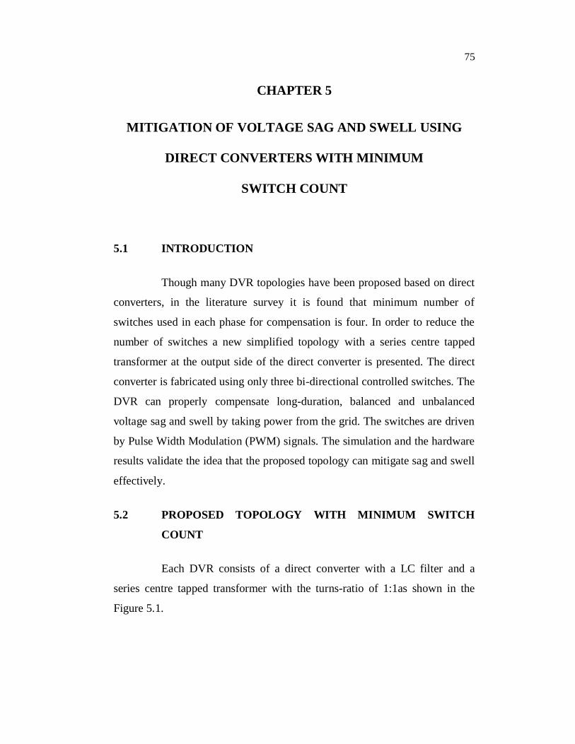
Each DVR consists of a direct converter with a LC filter and a
series centre tapped transformer with the turns-ratio of 1:1as shown in the
Figure 5.1.
76
Figure 5.1 Proposed topology with minimum switches
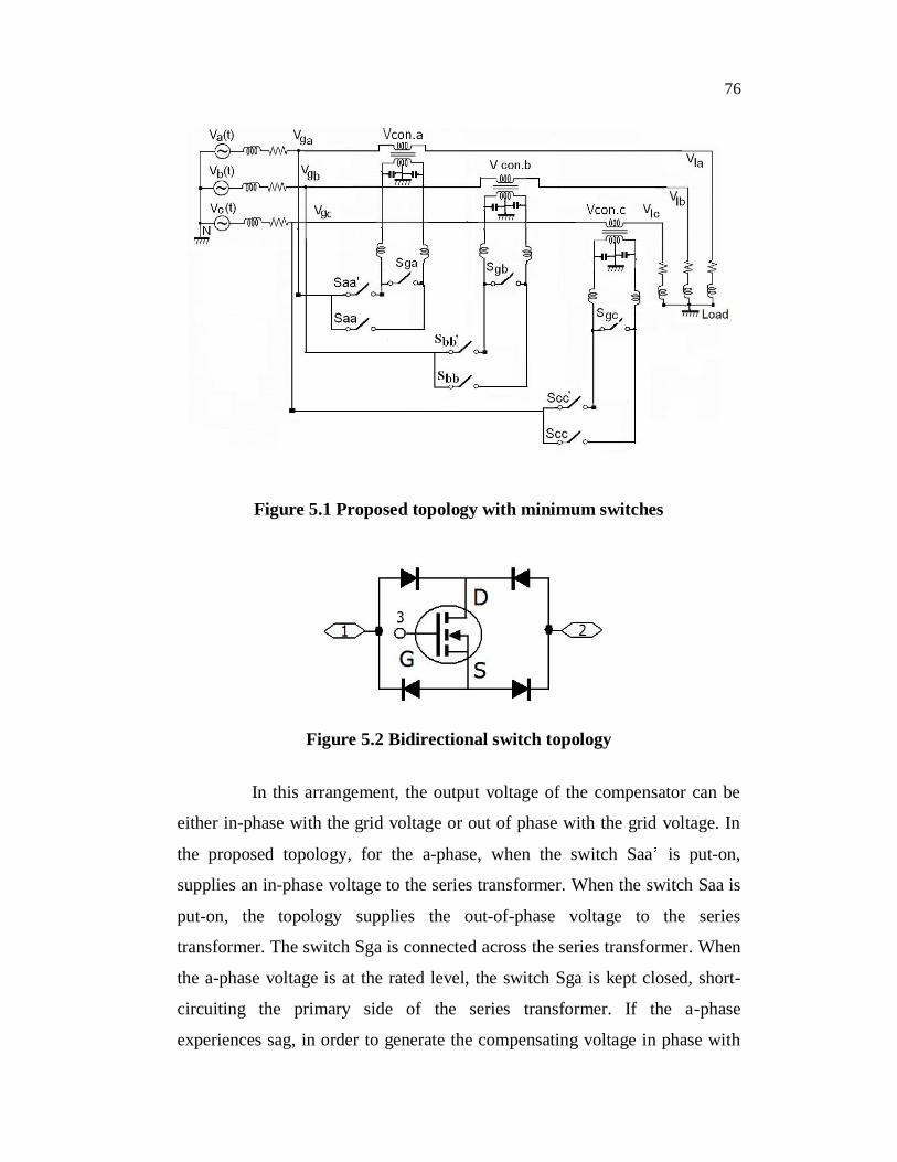
Figure 5.2 Bidirectional switch topology
In this arrangement, the output voltage of the compensator can be
either in-phase with the grid voltage or out of phase with the grid voltage. In
the proposed topology, for the a-phase, when the switch Saa is put-on,
supplies an in-phase voltage to the series transformer. When the switch Saa is
put-on, the topology supplies the out-of-phase voltage to the series
transformer. The switch Sga is connected across the series transformer. When
the a-phase voltage is at the rated level, the switch Sga is kept closed, short-
circuiting the primary side of the series transformer. If the a-phase
experiences sag, in order to generate the compensating voltage in phase with
77
the grid voltage, rnatively modulated. If it
has swell, then in order to generate the compensating voltage out of phase
with the grid voltage, the switches Saa and Sga are alternatively modulated.
The compensating voltage is added to the grid voltage through the
series transformer. Each DVR is structured by three bidirectional power
switches. The topology of the bidirectional switch used is shown in the
Figure 5.2. The switches are controlled by a simple PWM technique.
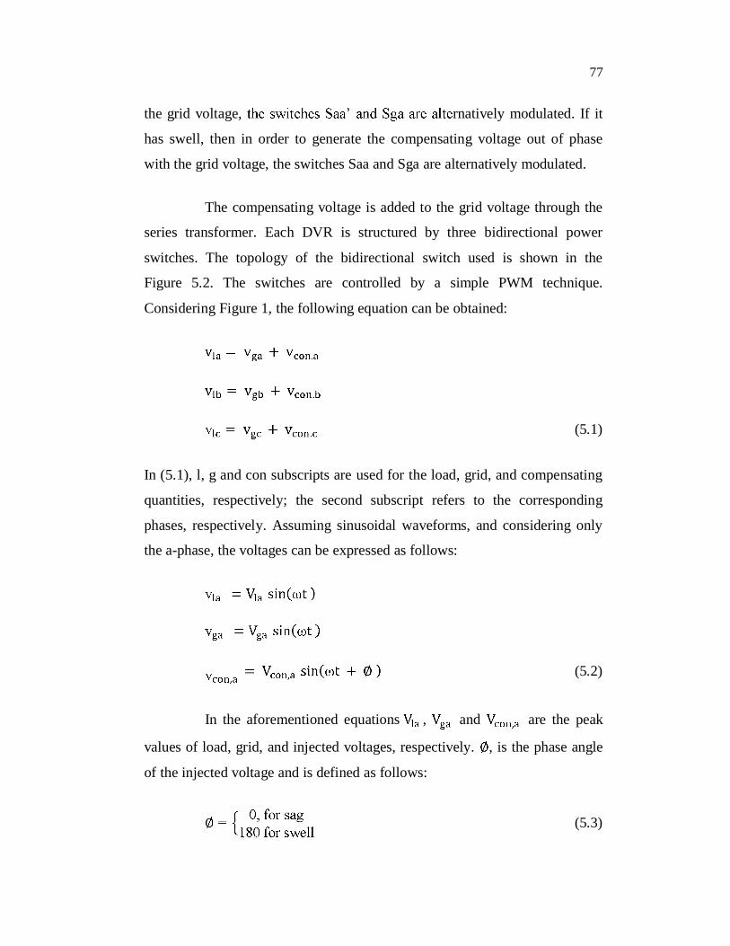
Considering Figure 1, the following equation can be obtained:
(5.1)
In (5.1), l, g and con subscripts are used for the load, grid, and compensating
quantities, respectively; the second subscript refers to the corresponding
phases, respectively. Assuming sinusoidal waveforms, and considering only
the a-phase, the voltages can be expressed as follows:
(5.2)
In the aforementioned equations , and are the peak
values of load, grid, and injected voltages, respectively. , is the phase angle
of the injected voltage and is defined as follows:
(5.3)

78
5.3 CONTROL PROCEDURE
As mentioned in the first chapter, the voltage sag and swell is
identified using single phase d-q theory. In this section switching pulse
generation for the mitigation of sag and swell is explained in detail.
5.3.1 Voltage Sag Mitigation
In order to compensate the voltage sag, it is necessary to inject
voltage in-phase with the grid voltage. As the centre tapped series transformer
gives output voltages of different polarity, the voltage which is in-phase with
the grid voltage is chosen. This voltage is modulated using bi-directional
switches and added in-phase with the grid voltage through a series
transformer.
Figure 5.3 Block diagram of switching pulse generation
So if the voltage sag has occurred in a-phase, then the bidirectional
A
detailed block diagram for switching pulse generation to mitigate the voltage
sag is shown in Figure 5.3. Ugmax has been obtained from single phase d-q
transform as explained in the first chapter. Uref is the desired terminal voltage,
which is a user specified constant value set in the micro controller program.

79
The difference between the reference voltage Uref and the peak value of the
grid voltage Ugmax gives the amount of voltage sag or swell in the grid. The
error signal is compared with the triangular carrier signal to generate the
switching pulses. The pwm pulses are given to the corresponding switches
through the logic gates as shown in the Figure 5.3.
5.3.2 Voltage Swell Mitigation
In order to compensate the voltage swell, it is necessary to inject
voltage out of phase with the grid voltage. So if there is voltage swell in phase
modulated to mitigate the swell. Switching pulse generation is same as that of
sag.
5.4 COMPENSATION RANGES OF THE DVR
In this section, the voltage sag and swell compensation ranges for
the proposed topology are calculated. It is assumed that the phase shift from
Vg to Vcon as well as the phase shift from Vcon to Vl are negligible. The
relationship between Vg and Vcon (the filtered output voltage of the converter)
can be expressed as
(5.4)
In (5.4
The above equation is valid because the transformation ratio of the series
transformer is 1:1.
5.4.1 Voltage Sag Compensation Range
According to Figure 1, for voltage sag condition:
(5.5)

80
Considering (5.4), (5.5) can be rewritten as follows:
(5.6)
The voltage sag percentage is defined by
(5.7)
Considering (5.6) and (5.7), the voltage sag percentage can be simplified to
(5.8)
It is seen that the maximum value of sag that can be compensated is
50% for D=1.
5.4.2 Voltage Swell Compensation Range
According to Figure 1, for voltage swell condition:
(5.9)
Considering (5.4), (5.9) can be simplified to
(5.10)
The voltage swell percentage is defined as follows:
(5.11)
Considering (5.10) and (5.11), the voltage swell percentage is
simplified as follows:
(5.12)

81
In this method the swell has been compensated by feeding the
voltage from the same phase. From (5.12) it is observed that for D = 0.5,
100% voltage swell can be compensated. As the value of D is increased the
topology can mitigate a greater amount of swell. It is not required to choose D
=1 to mitigate large swells since sufficient voltage is available in the phase
where swell is occurred.
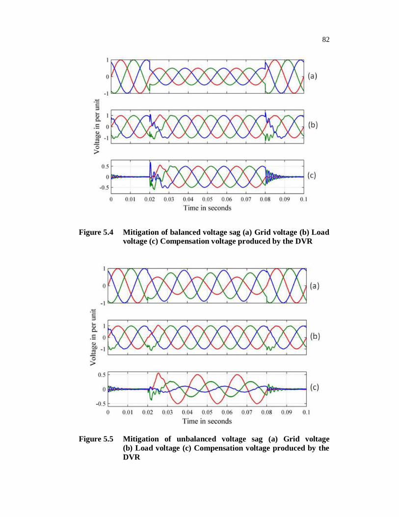
5.5 SIMULATION RESULTS
The MATLAB/SIMULINK software has been used for simulation.
Three phase RL load (0.8 power factor lag, 240VA per phase,) were
connected to the lines. The desired terminal voltage has been set at 60 V rms
(1p.u), 50 Hz. The switching frequency of the converters is 8 kHz. The filter
is designed for a cut off frequency of 1000Hz with the value of inductance
1.732mH and the capacitance of 15uF according to the formula f = 1/
The ability of the DVR to mitigate balanced voltage sag of 50% in
all the phases is shown in Figure 5.4.
Mitigation of unbalanced voltage sag
Figure 5.5.
The compensation of balanced swell of 100% is illustrated in
Figure 5.6.
The ability of the DVR to mitigate unbalanced voltage swell of
100% in a-phase, 50% in b-phase, and 25% in c-phase can be observed in
Figure 5.7.
82
Figure 5.4 Mitigation of balanced voltage sag (a) Grid voltage (b) Load voltage (c) Compensation voltage produced by the DVR
Figure 5.5 Mitigation of unbalanced voltage sag (a) Grid voltage (b) Load voltage (c) Compensation voltage produced by the DVR

83
Figure 5.6 Mitigation of balanced voltage swell. (a) Grid voltage (b) load Voltage (c) compensation voltage
Figure 5.7 Mitigation of unbalanced voltage swell (a) Grid voltage (b) Load voltage (c) Compensation voltage produced by the DVR

84
5.6 EXPERIMENTAL RESULTS
A three-phase DVR described in this chapter has been fabricated in
order to verify the design procedure. A photograph of the experimental
prototype is shown in the Figure 5.8. The PIC16F877A microcontroller has
been used to generate the switching pulses. The rating of the centre tapped
series transformer is 720VA, 120V with the transformation ratio of 1:1.
IRFP460 power MOSFET switches of rating 500V, 20A were used to
synthesize the direct converter. The hardware prototype has been designed for
a rated voltage of 60V.
Figure 5.8 Hardware prototype

85
The ability of the DVR to mitigate balanced voltage sag of 50% in all the
phases is shown in Figure 5.9.
Figure 5.9 Balanced Sag Compensation (a) Grid voltage (b) Compensated load voltage (c) Compensating voltage produced by the DVR

86
The compensation of unbalanced voltage sag of 50% in a-phase, 25% in b-
phase, and 10% in c-phase can be seen in Figure 5.10.
Figure 5.10 Unbalanced sag compensation (a) Grid voltage (b) Compensated load voltage (c) Compensating voltage produced by the DVR

87
The compensation of voltage swell of 90% in a-phase, 100% in b-phase, and
115% in c-phase can be seen in Figure 5.11.
Figure 5.11 Swell compensation (a) Grid voltage (b) Compensated load voltage (c) Compensating voltage produced by the DVR
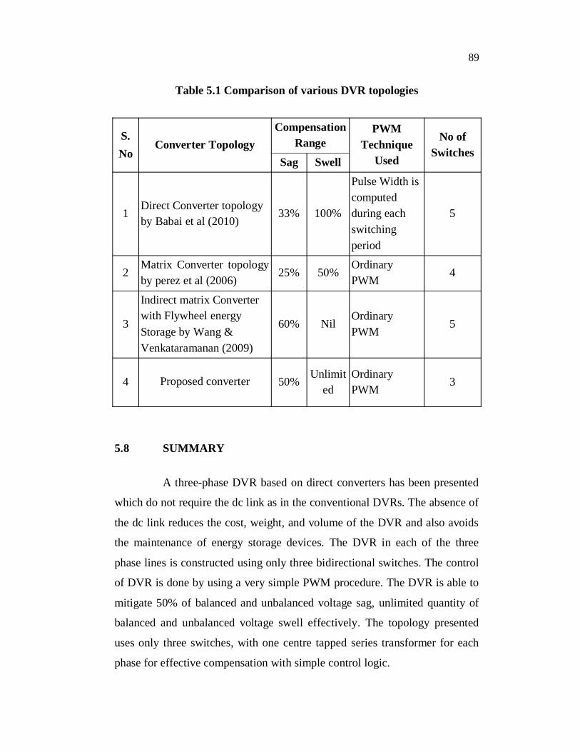
5.7 PERFORMANCE ANALYSIS
Babai et al (2010) proposed a topology based on direct converter,
with 5 switches per phase in which switches are controlled based on sampling
process and it needs computations throughout a cycle. Using the control
88
algorithm explained, the compensation range of voltage sag is 0-33% and of
the range for the voltage swell is 0-100%.
Perez et al (2006) presented a topology for a single-phase DVR
based on a single phase matrix converter with 4 switches per phase and the
compensation range is 25% for voltage sags and 50% for swells. In this
topology, during compensation 3 switches are modulated. So generation of
switching pulses is complicated.
Wang & Venkataramanan (2009) designed a DVR based on an
indirect matrix converter for balanced voltage sags compensation of 60%.
This topology needs flywheel energy storage element and the capability of the
topology in voltage swell compensation has not been investigated.
In this work, a centre tapped series transformer is used only with
3 bi-directional switches such that the only 2 switches are modulated
during compensation. So the switching loss is less and switching pulse
generation is also easier. In this topology switches are controlled by ordinary
PWM. As a result, computation is avoided, control is simpler and 50% of
voltage sag and unlimited quantity of voltage swell is compensated as
mentioned in Table 5.1.
89
Table 5.1 Comparison of various DVR topologies
S. No
Converter Topology Compensation
Range PWM
Technique Used
No of Switches
Sag Swell
1 Direct Converter topology by Babai et al (2010)
33% 100%
Pulse Width is computed during each switching period
5
2 Matrix Converter topology by perez et al (2006)
25% 50% Ordinary PWM
4
3
Indirect matrix Converter with Flywheel energy Storage by Wang & Venkataramanan (2009)
60% Nil Ordinary PWM
5
4
Proposed converter
50% Unlimit
ed Ordinary PWM
3
5.8 SUMMARY
A three-phase DVR based on direct converters has been presented
which do not require the dc link as in the conventional DVRs. The absence of
the dc link reduces the cost, weight, and volume of the DVR and also avoids
the maintenance of energy storage devices. The DVR in each of the three
phase lines is constructed using only three bidirectional switches. The control
of DVR is done by using a very simple PWM procedure. The DVR is able to
mitigate 50% of balanced and unbalanced voltage sag, unlimited quantity of
balanced and unbalanced voltage swell effectively. The topology presented
uses only three switches, with one centre tapped series transformer for each
phase for effective compensation with simple control logic.
![Enhancement of Power Quality by Optimal Placement of ...harmonics, unbalance and voltage sag using DVR has been suggested in [12]. Placement of DSTATCOM for mitigation of voltage sag](https://img.pdfslide.net/doc/110x75/5ed3304bf7f9301169375c90/enhancement-of-power-quality-by-optimal-placement-of-harmonics-unbalance-and.jpg)