Embed Size (px)
Citation preview

Chapter 5
PEDOT/Si/TiO2 Heterojunction
Solar Cells
5.1 Introduction
The work presented thus far has discussed the properties of two heterojunctions on
n-type silicon; PEDOT/Si and Si/TiO2. The data presented in Chapter 3 have shown
the PEDOT/Si heterojunction acts as an electron-blocking, hole-selective contact that
can be used in place of a p-n junction. The dark current in the PEDOT/Si device
is observed to be dominated by hole injection into the n-type silicon, which leads
to the need of a back-surface field for further J0 reduction. In Chapter 4, the band
alignments and surface passivation of the Si/TiO2 heterojunction were shown to fit the
requirements of a hole-blocking, electron selective contact which can potentially act
as a BSF for an n-type solar cell. The symmetry of these heterojunctions is valuable
in that they present two complementary contacts, which can combine to increase the
efficiency of a photovoltaic device. Furthermore, both heterojunctions were fabricated
without the use of any high-temperature diffusion steps as are typically required in
forming a p-n junction or n+-n BSF. Therefore, the use of a Si/TiO2 heterojunction
86

as a back surface field for a PEDOT/Si device to form a PEDOT/Si/TiO2 (PST)
solar cell represents the logical continuation of the work presented in the preceding
chapters.
The PST solar cell can be considered analogous to the HIT solar cell discussed in
Chapter 2. Figure 5.1 shows the band offsets of the PEDOT/Si and Si/TiO2 hetero-
junctions to the conduction and valence bands of silicon. Both rely on heterojunc-
tions to a lightly doped, high-quality wafer (rather than diffusing a conventional p-n
junction), however the HIT solar cell requires a plasma deposition process to form
amorphous-silicon heterojunctions. The growth of these amorphous silicon hetero-
junctions must be done carefully to avoid the formation of a heavily doped crystalline
layer [144]. Therefore, the PST not only represents a heterojunction solar cell fabri-
cated without a p-n junction, but also without any plasma deposition processes. In
addition, all processing temperatures used were below 250 C. In this chapter, the
dark current characteristics, photovoltaic performance, external quantum efficiency,
and charge storage behavior of the PST cell are presented and compared to those of
the single-sided PEDOT/Si device.
PEDOT
Silicon
LUMO
HOMO
∆ EC < 0.2 eV
∆ EV > 2.0 eV
∆ EV < 0.2 eV
TiO2
∆ EC = 0.5 eV
EC
EV
Figure 5.1: Band offsets of PEDOT:PSS and Titanium dioxide to crystalline siliconas measured by photoemission spectroscopy.
87

Blocked electron dark current
Photocurrent
Cathode(-)
n-SiAnode
(+)
PEDOT
Hole dark current
PhotocurrentLight
∆EC
VA
(a)
Blocked electron dark current
Photocurrent
Cathode(-)
n-SiAnode
(+)
PEDOT
Blocked hole dark current
Photocurrent
TiO2
Light
VA
(b)
Figure 5.2: Band diagrams of (A) single-sided PEDOT/Si photovoltaic device underillumination with small forward bias compared to a (B) PST device under similarconditions.
The introduction of a titanium dioxide hole blocker serves to reduce the dark
current in a PEDOT/Si device. As shown in Chapter 3, the current in a PEDOT/Si
device is dominated by hole current injected into the body of the n-type silicon from
the PEDOT:PSS. These injected holes can then recombine due to bulk recombination
or diffuse to the back at the back interface and recombine at the metal cathode. For
the high-lifetime silicon substrates used for the PST devices, the bulk recombination
time is long (≥1.0 ms) and the hole diffusion length Lp,N is much longer than the width
of the n-type quasi-neutral region W (Lp,N/W > 3). As a result, the device can be
considered to be in the short-base regime, and the majority of the injected holes from
the PEDOT:PSS will reach the cathode and recombine. The carrier paths within
such a device are presented in the band diagram of Figure 5.2a. By incorporating
a TiO2 hole-blocking layer at the cathode, these injected holes are presented with
an energetic barrier due to the valence band offset of the TiO2. Therefore, the dark
current flow due to these injected holes is reduced, as illustrated in Figure 5.2b.
In this chapter the effects of using TiO2 as a BSF to complement the PEDOT/Si
solar cell are presented. Section 5.2 discusses the fabrication of the PST solar cell.
Section 5.3 presents experimental data from the PST solar cells compared to PE-
DOT/Si devices, including dark current-voltage measurements (section 5.3.1), illu-
88

minated current-voltage measurements (section 5.3.2), external quantum efficiency
(section 5.3.3), and minority carrier storage (section 5.3.4). Section 5.4 shows the
effect that the thickness of the TiO2 has on the PST devices, and section 5.5 draws
conclusions form the experimental data presented.
5.2 Fabrication
Solvent Clean5 m Acetone + US5 m Methanol + US
5 m IPA + US
HF etch1 m in 20:1 H2O:HF
SC-115 m at 70ºC 5:1:1H2O:NH4OH:H2O2
HF etch1 m in 20:1 H2O:HF
SC-215 m at 70ºC 5:1:1
H2O:HCl:H2O2
CVD TiO2 deposition
HF etch1 m in 20:1 H2O:HF
Evaporate Al/Agback metal
Evaporate Ag top metal grid
Spin PEDOT:PSS210 s at 4300 rpm
FZ n-Si (300µm)
PEDOT (70nm)
Al/Ag (20/200nm)
TiO2 (4nm)
Ag grid (300nm)
1-sided HF etch1 m in 20:1 H2O:HF
Figure 5.3: Fabrication process and structure of PST solar cell.
The fabrication process of the PEDOT/Si/TiO2 Solar Cell is shown in Figure 5.3.
For the double-sided heterojunction solar cells, in order to reduce losses due to bulk
recombination, float-zone wafers with high bulk-lifetime were used, which had a phos-
phorus doping concentration of 1015 cm−3. These wafers had a thickness of 300 µm
and were double-side polished. The initial dicing and cleaning procedure of a solvent
clean with ultrasonic (US) agitation and RCA clean is identical to that of the single
sided PEDOT/Si device described in Section 3.2.
89

Immediately following the final HF dip of the cleaning procedure, the 16 mm×16 mm
silicon samples are placed into the TiO2 deposition chamber. The thin films are
deposited using the cycled growth method described in Section 4.2. For the devices
fabricated and discussed within this chapter a standard deposition of 3 cycles was
used (unless specified otherwise, as in section 5.4). Following the deposition of TiO2
the samples received evaporation of aluminum and silver metal to form the contact
on the cathode side of the device.
As described in Chapter 4, TiO2 is deposited on both sides (anode and cathode) of
the silicon samples during the low-temperature CVD process. The TiO2 on the anode
side of the sample is etched away with the use of a PDMS mold, which allows the
application of 20:1 H2O:HF acid to only one side of a 16 mm×16 mm sample (shown
schematically in Figure 5.4). This allows the TiO2 on the cathode side to remain
while the anode side is etched. Immediately following the HF acid etch, the sample is
rinsed with deionized water, blown dry using N2, and the anode side of the device is
spin-coated with PEDOT:PSS at 4300 rpm. After PEDOT:PSS coating the samples
are then placed under vacuum for thermal evaporation of the front side metal grid.
Three grid designs were used that covered 5.4 %, 9.7 %, and 16.2 % of the top surface
area of the device. The grid layouts are shown in section A.1.
FZ n-Si
TiO2
PDMSHF
Solution
TiO2
Figure 5.4: Schematic of PDMS mold used to etch TiO2 from only one side of thesilicon sample.
90

- 0 . 4 - 0 . 2 0 . 0 0 . 2 0 . 4 0 . 6 0 . 8 1 . 01 0 - 9
1 0 - 7
1 0 - 5
1 0 - 3
1 0 - 1
T i O 2Cu
rrent
Dens
ity (A
cm-2 )
V o l t a g e ( V )
N o T i O 2
(a)
4 8 0 5 0 0 5 2 0 5 4 0 5 6 0 5 8 0 6 0 0 6 2 0
1 0 - 3
1 0 - 2
2 0 m V
Curre
nt De
nsity
(A cm
2 )
V o l t a g e ( m V )
T i O 2
N o T i O 2
(b)
Figure 5.5: (A) Current-density vs voltage characteristics of single-sided and PSTsolar cell in the dark. (B) Close-up of ideal (n=1) exponential region showing ∼20 mVshift
5.3 Performance of TiO2 Hole Blocker as a Back-
Surface-Field
The following sections seek to experimentally demonstrate the performance of TiO2
as an effective hole blocker in photovoltaic devices. To that end, the double-sided het-
erojunction device (PEDOT/Si/TiO2) is compared to a single-sided heterojunction
device (PEDOT/Si). Section 5.3.1 looks at the effect that TiO2 has on the current-
voltage characteristics of solar cells in the dark, while Section 5.3.2 presents the data
obtained under AM1.5G illumination. Section 5.3.3 shows the effect of TiO2 on ex-
ternal quantum efficiency (EQE) measurements. Section 5.3.4 presents the effect that
TiO2 has on the stored charge within the device as measured by reverse recovery.
5.3.1 Dark Current-Voltage Characteristics
The current density-voltage (J-V) characteristics of a PEDOT/Si and PEDOT/Si/TiO2
(PST) device as measured in the dark are presented in Figure 5.5a. Both devices
show some non-ideal (n>1) current in reverse and low forward bias (<0.4 V). The
91
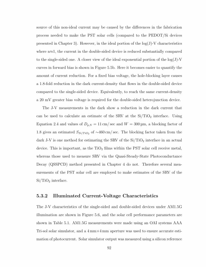
source of this non-ideal current may be caused by the differences in the fabrication
process needed to make the PST solar cells (compared to the PEDOT/Si devices
presented in Chapter 3). However, in the ideal portion of the log(J)-V characteristics
where n≈1, the current in the double-sided device is reduced substantially compared
to the single-sided one. A closer view of the ideal exponential portion of the log(J)-V
curves in forward bias is shown in Figure 5.5b. Here it becomes easier to quantify the
amount of current reduction. For a fixed bias voltage, the hole-blocking layer causes
a 1.8-fold reduction in the dark current-density that flows in the double-sided device
compared to the single-sided device. Equivalently, to reach the same current-density
a 20 mV greater bias voltage is required for the double-sided heterojunction device.
The J-V measurements in the dark show a reduction in the dark current that
can be used to calculate an estimate of the SRV at the Si/TiO2 interface. Using
Equation 2.4 and values of Dp,N = 11 cm/ sec and W = 300 µm, a blocking factor of
1.8 gives an estimated SSi/T iO2 of ∼460 cm/ sec. The blocking factor taken from the
dark J-V is one method for estimating the SRV of the Si/TiO2 interface in an actual
device. This is important, as the TiO2 films within the PST solar cell receive metal,
whereas those used to measure SRV via the Quasi-Steady-State Photoconductance
Decay (QSSPCD) method presented in Chapter 4 do not. Therefore several mea-
surements of the PST solar cell are employed to make estimates of the SRV of the
Si/TiO2 interface.
5.3.2 Illuminated Current-Voltage Characteristics
The J-V characteristics of the single-sided and double-sided devices under AM1.5G
illumination are shown in Figure 5.6, and the solar cell performance parameters are
shown in Table 5.1. AM1.5G measurements were made using an OAI systems AAA
Tri-sol solar simulator, and a 4 mm×4 mm aperture was used to ensure accurate esti-
mation of photocurrent. Solar simulator output was measured using a silicon reference
92

cell (PV Measurements Inc.) that was calibrated using Newport Corporations PV
Cell Lab. All calculations use total device area (4 mm×4 mm), including the metal-
ized grid, which covered about 16 % of the device surface for the data shown Figure 5.6
and Table 5.1. The double-sided device shown exhibits a significant improvement over
the single-sided device of over 30 mV in VOC . This is further evidence that the dark
current is reduced at the Si/TiO2 interface due to the hole-blocker, as this increase in
VOC agrees to first order with the shift observed in the dark current characteristics.
- 0 . 4 - 0 . 2 0 . 0 0 . 2 0 . 4 0 . 6 0 . 8- 4 0- 3 0- 2 0- 1 0
01 02 03 04 0
A M 1 . 5 G
T i O 2
Curre
nt De
nsity
(mA c
m-2 )
V o l t a g e ( V )
N o T i O 2
Figure 5.6: Current-voltage characteristic of a PEDOT/Si solar cell with and withoutTiO2 hole blocker under AM1.5G illumination.
Table 5.1: Performance parameters of PEDOT/Si and PEDOT/Si/TiO2 solar cells
Device VOC(mV) JSC(mA cm−2) FF (%) η(%)
No TiO2 583 22.9 77.1 10.3
With TiO2 614 24 76.2 11.2
∆ +31 +1.1 -0.9 +0.9
93

The measured improvement in open-circuit voltage ∆VOC can also provide an
estimate of the SRV at the Si/TiO2 interface. Using the observed open-circuit voltages
of the devices presented in Table 5.1 and Equation 2.7, the SRV at the Si/TiO2
interface can be estimated to be ∼170 cm s−1. However, this contrasts to the value
estimated from dark J-V measurements of ∼460 cm/ sec for the Si/TiO2 interface.
It is useful to also consider the average values of VOC of the devices. The average
and standard deviation of VOC for eighteen PEDOT/Si devices and eighteen PST
devices are (588± 4) mV and (613± 5) mV, respectively, which provides an average
value of ∆VOC of (25± 7) mV. This leads to an estimate of SRV between 150 cm s−1
to 360 cm s−1, a range which is closer to the value estimated from the dark J-V
measurement.
It is also possible that the disagreement in the SRV estimation may be due in part
to the control device suffering from a parasitic barrier at the back contact. The par-
asitic back contact and the backside scribing used to mitigate its effect are discussed
in Section A.2. However, it is possible that even with the backside scribing, there
is a finite parasitic barrier still present at the back contact. This would artificially
lower the VOC of the single sided device, increasing ∆VOC and decreasing the calcu-
lated value of the SRV. This is further discussed within the experimental conclusions
presented in section 5.5.
The hole-blocking TiO2 layer also improves the short-circuit current density
in the PST device. The single-sided device exhibits a short-circuit current of
22.9 mA cm−2, while the double-sided device achieved a JSC of 24.0 mA cm−2, an
increase of 1.1 mA cm−2. On average (for 16 % coverage of the top metal grid), the
JSC of single-sided devices was (22.8± 0.5) mA cm−2 and of double-sided devices
was (23.6± 0.4) mA cm−2, a difference of 0.8 mA cm−2. The increase in short-circuit
current density can be attributed to reduced recombination at the rear interface of
94

the solar cell due to the TiO2 hole blocker, which will be discussed in the following
section.
Overall, the PST device shows an absolute improvement of 0.9 % (8.7 % relative)
in power conversion efficiency over the device without any TiO2 hole blocker. The
small decrease in FF observed is a relative change of just −1.2 %, and while this may
be due to the incorporation of the TiO2 layer, it does not significantly hamper the
performance of the PST device.
5.3.3 External Quantum Efficiency
The external quantum efficiency measurements also demonstrate the ability of the
TiO2 to reduce hole recombination at the back interface. The EQE spectra for a
single-sided device and double-sided device are shown in Figure 5.7. It is clear from
the optical modeling presented in Section 3.6 that PEDOT:PSS does not serve as an
ideal anti-reflective coating. There is loss in the EQE spectra due to both surface
reflection and absorption in the PEDOT:PSS, as predicted by the modeling performed
in section 3.6. However, of the most interest is the difference in the spectra of the
PST device and the single-sided device towards longer wavelengths (from 700 nm to
1050 nm).
Lower energy photons – those with longer wavelengths– are absorbed poorly in
silicon. Figure 5.8 shows the absorption depth vs wavelength for silicon [145]. As
the wavelength of light increases, so does the absorption depth, meaning that the
profile of absorbed carriers in silicon extends further into the silicon. Since optical
absorption directly leads to carrier generation in the silicon, for a given intensity,
longer wavelength light is more likely to generate carriers at the back of the solar
cell, near the Si/TiO2 interface. The optical generation in the silicon can be written
as in Equation 5.1, where G0 is the generation rate at the surface of the absorber
material, and αabs is the inverse of the absorption depth, also known as the absorption
95

3 0 0 4 0 0 5 0 0 6 0 0 7 0 0 8 0 0 9 0 0 1 0 0 00 . 00 . 10 . 20 . 30 . 40 . 50 . 60 . 70 . 80 . 9
EQE
W a v e l e n g t h ( n m )
N o T i O 2
T i O 2
Figure 5.7: External quantum efficiency spectra of double sided and single-sideddevices.
coefficient.
Glight(x) = G0 exp (−xαabs) (5.1)
The normalized generation rate is plotted as a function of depth in the silicon
for several wavelengths in Figure 5.9, and illustrates how longer wavelength light
4 0 0 6 0 0 8 0 0 1 0 0 0 1 2 0 0 1 4 0 01 0 - 61 0 - 51 0 - 41 0 - 31 0 - 21 0 - 11 0 01 0 11 0 21 0 31 0 41 0 51 0 61 0 7
Abso
rption
depth
(cm)
W a v e l e n g t h ( n m )Figure 5.8: Absorption depth versus wavelength for crystalline silicon [145]
96

0 5 0 1 0 0 1 5 0 2 0 0 2 5 0 3 0 00 . 0
0 . 5
1 . 0
Norm
alized
Gen
eratio
n Rate
(cm-3 )
D e p t h ( m i c r o n s )
λ = 9 0 0 n mλ = 1 0 0 0 n m
λ = 8 0 0 n mλ = 8 0 0 n m
Figure 5.9: Normalized generation rate as a function of depth in silicon for severalwavelengths
generates more carriers deeper in the silicon. Thus, these wavelengths will be more
sensitive to reduced recombination due to the TiO2 hole-blocker.
The EQE of the double-sided device is shown normalized to the EQE of the single-
sided device in Figure 5.10. It is clear that for wavelengths >800 nm, the EQE of the
double-sided device is higher than that of the single-sided device. The improvement in
the EQE of the double sided device increases as the wavelength increases, as is made
apparent by the normalized EQE. The normalized EQE can also be used to calculate
the difference in JSC for the two devices, or ∆JSC . The calculation is performed by
using Equation 5.2, where ∆EQE(λ) is the difference in EQE between the single
sided and double sided devices and S(λ) is the spectral irradiance, in this case the
AM1.5G spectrum. The spectral irradiance represents the energy per square meter
per wavelength which is incident on the solar cell. This is divided by the energy per
photon at each wavelength to give the number of photons absorbed per wavelength.
The ∆EQE(λ) represents the percentage of these photons which generate carriers
97

7 0 0 8 0 0 9 0 0 1 0 0 01 . 0
1 . 1
1 . 2
1 . 3
1 . 4
1 . 5
S = 3 0 0D e v i c e
S = ∞S = 1 0 0 0No
rmaliz
ed EQ
E
W a v e l e n g t h ( n m )
S = 0S = 1 0 0
Figure 5.10: EQE of double-sided device normalized to the single-sided device. Datais compared to modeled spectra with various SRV or S values for the Si/TiO2 interface.
which are collected and contribute to photocurrent in the double sided device which
are not collected by the single sided. Therefore, integrating over all wavelengths yields
a ∆JSC of 1.1 mA cm−2, in agreement with the observed increase in photocurrent
measured in Figure 5.6.
∆JSC =q
hc
∫∆EQE(λ)S(λ)λ∂λ (5.2)
The improvement in the EQE, ∆EQE, depends on the SRV or S at the Si/TiO2
interface. The optical generation profile can be used along with the continuity equa-
tion to calculate how many carriers will be collected at the front junction in the EQE
measurement. For the single-sided device, recombination at the rear interface is es-
sentially infinite. Therefore the boundary condition here is that the recombination
current is limited by how fast the carriers can diffuse to the interface. For the double-
sided device, the boundary condition is determined by the surface recombination at
that interface. This is modeled numerically for several values of SRV of the Si/TiO2
98

interface in figure 5.10. As Figure 5.10 shows, the data agree best with a modeled
SRV of 300 cm s−1.
5.3.4 Stored Minority Carrier Charge
The effectiveness of the TiO2 hole-blocking layer can also be determined by measuring
the stored minority hole charge Qstored in the neutral n-type silicon of the device under
forward bias. For the same current in forward bias, and thus the same slope of the
hole concentration profile, the double-sided device will contain a greater Qstored as
indicated by the crosshatched area in Figure 2.3b. The reverse recovery method [78–
85] was used to estimate Qstored in the PST and single-sided devices. As described
in Chapter 3, the reverse recovery measurement is performed by alternately forward
biasing and reverse biasing the device. Under reverse bias, a transient reverse current
IR can be observed.
The reverse current is due to the holes leaving the silicon back to the PEDOT and
will continue to flow up to a time tstore, at which point the hole concentration at the
edge of the depletion region reaches equilibrium value, and IR begins to fall. Qstored
is approximated by the product of IR and tstore.
Figure 5.11 shows IR as a function of time for a single-sided and a double-sided
device. The double-sided device maintains a flow of IR for a three-fold longer tstore,
and therefore contains approximately a three-fold greater initial Qstored compared to
the single-sided device without TiO2.
The stored charge measurement can also provide an estimate of the surface re-
combination velocity. Assuming minimal bulk recombination, the stored charge of
the single sided device Qstore,SS is represented by the area under the minority carrier
profile shown in Figure 2.3b and is given by Equation 5.3
Qstore,SS =p′SS(0)W
2(5.3)
99

- 5 0 0 5 0 1 0 0 1 5 0 2 0 0- 5- 4- 3- 2- 10
1 01 52 02 53 0
Curre
nt (m
A cm-2 )
T i m e ( µ s )
N o T i O 2 T i O 2
Figure 5.11: Reverse current as a function of time for the PST and single-sided solarcell in the reverse recovery experiment
Similarly, the stored charge within the double-sided device Qstore,DS is given by Equa-
tion 5.4.
Qstore,DS = Wp′DS(W ) +p′SS(0)W
2(5.4)
Taking the ratio of the stored charge yields Equation 5.5.
Qstore,DS
Qstore,SS
= 2p′DS(W )
p′SS(0)+ 1 (5.5)
The forward current in the single sided device is dependent on the diffusion profile
of holes in Equation 2.2 must equal the current due to holes recombining at the
Si/TiO2 interface given by Equation 2.3. Combining Equation 2.2 and Equation 2.3
yields an expression for p′DS(W )/p′SS(0), and substituting this into Equation 5.5 yields
Equation 5.6, in which the ratio of stored charge depends directly on the SRV of the
TiO2 hole-blocker.
SSi/T iO2 =Dp,N
2W
(Qstore,DS
Qstore,SS
− 1
)(5.6)
100

Using the data from Figure 5.11, the ratio of the stored charge is 2.72 and the
estimated SRV from the charge storage measurement is 345 cm s−1. It should be noted
that this is only a first order estimate, as it neglects the effect of recombination at the
back and front interfaces during both the forward bias and reverse bias phase. More
precise modeling incorporating recombination during the reverse bias phase is being
carried out by Alexander Berg in our lab and will be reported elsewhere.
5.4 Thickness effects of TiO2 films
Thus far, the discussion of PST solar cells has not considered the effect of the TiO2
thickness. As this section will show, the thickness of the TiO2 film can have a signif-
icant impact on performance of the PST solar cells. Initial attempts at fabricating
PST solar cells with thin (< 2.5 nm) films of TiO2 were observed to be insufficient
to provide good hole-blocking properties. The poor performance of thin TiO2 films
motivated the growth thicker films of TiO2. However, the TiO2 thickness obtained
from the method introduced in Chapter 4 was observed to saturate with multiple de-
position cycles around 4 nm. Modified deposition methods were therefore developed
for obtaining thicker (> 4 nm) TiO2 films, and these films were incorporated into PST
devices.
The modification of the growth process in order to achieve thicker TiO2 layers
is presented in section 5.4.1. The mechanisms underlying the poor performance of
thin TiO2 films in PST solar cells are presented in section 5.4.2. The mechanisms
underlying the performance of thick (> 4 nm) TiO2 films are presented in section 5.4.3.
5.4.1 Modified Growth Process for Thick TiO2
The first approach to grow thicker layers was to simply increase the number of adsorp-
tion and thermolysis cycles used in the low-temperature CVD process described in
101

TimeTe
mp.
Adsorption
Thermolysis
1 cycle Repeat for N-cycles
Remove samples
-10ºC
100ºC
(a)
3 cycles Additional cycles
Remove samples
Time
Tem
p.
-10ºC
100ºC
Vent Chamber
Vent Chamber
Additional cycles
(b)
Figure 5.12: (A) standard TiO2 deposition process using multiple cycles and (B)modified process with chamber vent between additional cycles. All adsorption andthermolysis times were kept constant at 10 min, and the chamber vent was typically1 min to 5 min
Chapter 4. The hypothesis was that more of the titanium alkoxide precursor would
adsorb and thermolyze with each subsequent cycle, increasing the thickness of the
overall film. This process is shown schematically in Figure 5.12a. In this approach,
samples are placed into the chamber and undergo a set amount of repeated cycles
before removal.
However, the thickness of TiO2 layers obtained by simply increasing the number of
cycles was observed to saturate, as shown by Figure 5.13. These data points represent
samples that underwent multiple cycles (with the exception of the 1-cycle data point)
before removal from the chamber. It is hypothesized that the presence of unreacted
organic groups left from incomplete decomposition of the titanium(IV) tetra-(tert-
butoxide) precursor on the surface of the TiO2 film can prevent the adsorption of
more precursor. If no precursor molecules adsorb to the surface of the film, then
there is no TiO2 created during the thermolysis step and the thickness of the film
does not increase with further cycling. As a result, the growth of the TiO2 films is
observed to saturate at ∼3 nm to 4 nm, as shown.
To facilitate decomposition of the organic groups that may be present on the
surface of the TiO2 film, the introduction of oxygen and water vapor from laboratory
ambient was investigated. Since the titanium(IV) tetra-(tert-butoxide) precursor is
102

0 1 2 3 4 5 6 7 8 9 1 012345678
TiO2 T
hickn
ess (
nm)
N u m b e r o f C y c l e s
W i t h V e n t i n g
N o V e n t i n g
Figure 5.13: Thickness of TiO2 films versus number of cycles using venting process(hollow circles) and without venting (filled circles).
quickly broken down upon exposure to oxygen and water vapor, it was hypothesized
that exposure to laboratory ambient would allow unreacted organic groups on the
surface of the TiO2 film to decompose. By reacting the surface organic groups, the
titanium alkoxide should then able to adsorb to the TiO2 surface, resulting in more
TiO2 deposition upon further cycling.
Laboratory ambient was introduced by venting the deposition chamber between
cycles, as shown schematically in Figure 5.12b. After a number of cycles (typically 3),
the chamber is vented and exposed to laboratory ambient for 1 min to 5 min. Then
the chamber is pumped back down and additional cycles are run to add thickness to
the TiO2 film. Venting the chamber was observed to prevent the saturation of TiO2
thickness with additional cycles, as shown in Figure 5.13. For the data shown, 3 cycles
were run for the inital TiO2 film, which resulted in ∼2.7 nm thickness. By venting
the chamber and then running an additional 2 cycles, the thickness was increased to
∼3.8 nm, then ∼5.5 nm, and finally a ∼6.8 nm film was achieved.
103

Another growth method (which was developed by Gabriel Man) was investigated
which uses a controlled pulse of vapor pressure from the precursor vial to obtain
thicker TiO2 growth. The process nominally follows the same procedure as the stan-
dard method described in Chapter 4, yet with a precursor valve that can be carefully
controlled (The chamber used also has a slightly different geometry, however this is
not anticipated to cause a difference). This method controls the opening speed of
the precursor bulb in order to obtain a spike in the chamber base pressure. It is
hypothesized that the spike in pressure is due to a burst of precursor vapor entering
the chamber, which results in a thick coating of adsorbed precursor onto the samples.
As a result, this method is observed to obtain TiO2 films that are 5 nm to 12 nm
thick, depending on location within the chamber.
0 1 2 3 4 5 6 7 8 9 1 0 1 1 1 2- 2 0- 1 5- 1 0- 505
1 01 52 02 53 03 54 0
P u l s e dm e t h o d
S t a n d a r d m e t h o d
∆VOC
(mV)
T i O 2 T h i c k n e s s ( n m )
V e n t i n gm e t h o d
Figure 5.14: ∆VOC as a function of the thickness of the TiO2 hole blocking film in PSTsolar cells for various growth methods. Error bars represent the standard deviationof a batch of nine devices
The various growth methods discussed were used to deposit TiO2 films for in-
corporation into PST solar cells, and the improvement in VOC over the PEDOT/Si
104

control devices is shown in Figure 5.14. For TiO2 films deposited using the standard
growth procedure, a problem is observed in which TiO2 films that are too thin do not
demonstrate improvement in VOC . Another issue is observed for TiO2 films obtained
using the venting growth process, in which the improvement in VOC is observed to
decrease with thicker films. Finally, experiments with the pulsed vapor deposition
method show encouraging results for thick TiO2 films, in contrast to the venting
method. The mechanisms behind these observations are discussed in the following
sections.
5.4.2 ‘Thin’ TiO2 and Aluminum Interaction
The requirements of a hole-blocking heterojunction, as outlined in Chapter 2, are hav-
ing the correct band alignments and providing good surface passivation of crystalline
silicon. The photoemission spectroscopy (PES) and Quasi-Steady State Photocon-
ductance Decay (QSSPCD) measurements presented in Chapter 4 show that TiO2
satisfies both of these requirements. Therefore, one would predict good performance
from these films when incorporated into PST solar cells as BSFs. However, the fabri-
cation process of a PST solar cell differs from that of a PES or QSSPCD measurement
sample in that the TiO2 is metalized. Metal deposition on top the TiO2 film is re-
quired in order to form the cathode contact of the PST solar cell, whereas for PES
or QSSPCD measurements the sample is comprised of a bare TiO2 film on silicon.
The metalization process can have a significant effect on the performance of the
PST solar cells. This is not surprising considering the impact that metalization had
on the performance of the p-type Si/TiO2 diodes discussed in Chapter 4. As is the
case with the p-type diodes, in the PST devcies, the metal used to contact the TiO2 is
aluminum and is deposited via thermal evaporation. The evaporator used to deposit
the aluminum for all devices presented in this chapter was the Edwards 306 system,
which was shown to provide good p-type diodes. However, in a PST solar cell there
105

4 6 8 4 6 4 4 6 0 4 5 64 06 08 0
1 0 01 2 01 4 01 6 01 8 0 X P S o f T i 2 p c o r e l e v e l : T i O 2 / n - S i
Photo
electr
on co
unt (c
ps)
B i n d i n g e n e r g y ( e V )
T i 4 + a t4 5 9 . 5 6 e V
T i 0 +T i 2 +T i 3 +T i 4 +
(a)
4 6 8 4 6 4 4 6 0 4 5 63 54 04 55 05 56 06 57 0
T i 0 +T i 2 +T i 3 +T i 4 +
X P S o f T i 2 p c o r e l e v e l : A l / T i O 2 / n - S i
Photo
electr
on co
unt (c
ps)
B i n d i n g e n e r g y ( e V )
T i 4 + a t4 5 9 . 7 2 e V
T i 3 + a t4 5 7 . 9 7 e V
(b)
Figure 5.15: XPS scan of the titanium 2p core levels in a TiO2 films on siliconsubstrate (A) without metal and (B) with thin (1 nm to 2 nm) film of Al. Dottedlines indicate measured spectra, solid lines indicate fitted Gaussian-Lorentz peaks, andthin dashed line indicated background noise. A range of binding energies is shownfor the Ti2p3/2 level for Ti in the Ti4+, Ti3+, Ti2+, and Ti0+ oxidation states, fromthe NIST database (Such reported values are useful only as a rough guide, as theyare taken from measurements of bulk films, the binding energies of which can differsignificantly from those of thin films, such as in this work). Measurement courtesy ofGabriel Man.
is no band-bending at the Si/TiO2 interface as in the p-type diode, and therefore this
interface is more sensitive to recombination.
X-Ray Photoemission Spectroscopy measurements revealed the effects of alu-
minum metalization on the TiO2 films. The thermal evaporation process facilitates
an interaction between the aluminum film and the TiO2 in which the Al is oxidized
and a mixed oxide is formed. Evidence for this reaction can be seen by scanning the
titanium 2p core levels. A typical TiO2 film deposited via low-temperature CVD only
shows titanium in the Ti4+ state, as shown in Figure 5.15a. This is indicative of a
stoichiometric TiO2 film, as discussed in Chapter 4 and in previous work [39].
However, Figure 5.15b shows that after aluminum evaporation, the composition of
the TiO2 film changes. In addition to the Ti4+ peaks, an additional peak is observable
at lower binding energy. The peak is located at ∼2 eV lower binding energy (a very
106

significant shift in the binding energy), and therefore indicates that this peak arises
from titanium in the Ti3+ oxidation state. Therefore the XPS data provides evidence
that the stoichiometric TiO2 film changes chemically into a mixed AlxTiyOz oxide. In
the formation of such a mixed oxide, if the aluminum reacts with the TiO2 film it may
also consumes a portion of it. It is speculated that the consumption of the TiO2 film
results in a thinner film, which leads to degraded hole-blocking of the heterojunction
due to tunneling, and poorer PST devices.
5.4.3 Properties of ‘Thick’ TiO2
The achievement of thicker TiO2 films using the venting growth process was envisioned
to enhance the open-circuit voltage achieved by the double-sided heterojunction de-
vices. However, as Figure 5.14 shows, as the thickness of the TiO2 films is increased
with the venting method, the open-circuit voltage gain of the PST devices decreases
to the point of becoming negative. The fact that VOC begins to decrease below that
of the control devices suggests that there is a parasitic effect happening due to the
thicker films. One hypothesis is that the films may contain some form of trapped
charge which causes a parasitic barrier, similar to that discussed in Section A.2. In
this hypothesis, negative charges in the TiO2 film would cause a shift downward in
the Fermi level and upwards in the conduction band. Therefore, while there is no
barrier to electrons in the silicon conduction band normally, negative charges in the
TiO2 may cause band-bending that results in a barrier. When excess electrons are
generated due to photocurrent, they would normally simply diffuse to the cathode.
However if a barrier is present in the conduction band of the TiO2, a voltage drop
would form in order to lower the barrier presented by the electric field of the conduc-
tion band, as is illustrated in Figur 5.16. This voltage would lower the open-circuit
voltage achieved by the device just as in the case of the parasitic Schottky barrier
contact discussed in Section A.2.
107

Voc loss
Photo-current
n-SiAnode(+)
PEDOT Photo-currentLight
Parasitic barrier
Cathode(-)
e-e-
e-
e-
Acceptor defects
TiO2
Figure 5.16: Band diagram illustration of a PEDOT/Si/TiO2 solar cell showing neg-ative charges causing a barrier for electrons at the cathode contact.
1 8 1 6 1 4 1 2 1 0 8 6 4 2 0
Photo
electr
on co
unt (c
ps)
B i n d i n g e n e r g y w . r . t . E F ( e V )
E V = 3 . 1 6 e V w . r . t . E F
U P S H e I I o f ~ 2 . 5 n m T i O 2
(a)
1 8 1 6 1 4 1 2 1 0 8 6 4 2 0
Photo
electr
on co
unt (c
ps)
B i n d i n g e n e r g y w . r . t . E F ( e V )
E V = 2 . 9 9 e V w . r . t . E F
U P S H e I I o f ~ 5 n m T i O 2M u l t i - c y c l e w i t h v e n t i n g
(b)
Figure 5.17: UPS HeII scans showing valence band of (A) ∼2.5 nm TiO2 and (B)∼5 nm TiO2 grown by venting process.
To study the mechanism behind the open-circuit voltage loss, photoemission spec-
troscopy was used to compare thick (5.2 nm) TiO2 and thin (2.4 nm) TiO2 films. UPS
measurements showed that the valence band edge in the case of the thick TiO2 films
were shifted by 0.17 eV closer to the Fermi level than the case of the thin TiO2, as
shown by the HeII spectra shown in Figure 5.17. This ∼0.2 eV shift was mirrored
in the IPES spectra of the conduction band states, the XPS spectra of the titanium
2p levels, and the oxygen 1s levels. This spectroscopy data show that the band
alignments have not changed, rather the band bending in the silicon has changed.
108

The band bending of the silicon upwards at the Si/TiO2 interface increases as a
result of the thick TiO2 film by ∼0.1 eV. A comparison of the band bending resulting
from the different films is illustrated in Figure 5.18. These measurements support
the stated hypothesis that there is a detrimental barrier being formed in the silicon
conduction band due to thicker films of TiO2.
n-Si
∆EV > 2.0 eV
∆EC < 0.2 eV
EC
EV
TiO2
SiBB 0.3 eV
n-Si
∆EV > 2.0 eV
∆EC < 0.2 eV
EC
EV
Thick TiO2
SiBB 0.4 eV
Figure 5.18: Comparison of band alignment for thin and thick TiO2 films on n+
silicon as measured by PES techniques by Gabriel Man. The band alignment of theThick TiO2 films show an increase the bending of the conduction band upwards,which supports the theory of thick TiO2 films leading to a parasitic barrier at theback contact.
While the PST device data and photoemission spectroscopy data both support the
hypothesis regarding negative charge, the source of these negative charges is not clear.
One possibility is that the venting process introduces contaminants to the surface of
the TiO2 that become trapped as subsequent layers are grown. This hypothesis is also
supported when considering the data from the PST solar cells which are fabricated
using the pulsed vapor method. This method also achieves thick layers of TiO2,
however, improvement in the VOC of PST devices which use these thick films is also
observed and is shown in Figure 5.14. This shows that the ∆VOC loss is not inherently
due to thick TiO2, but rather the method in which the thick layers are deposited.
This therefore supports the possibility that the laboratory ambient is introducing
contamination into the venting method.
109

5.5 PEDOT/Si/TiO2 Solar Cell Conclusions
5.5.1 Summary of SRV Estimates
The data from the four measurements presented in Sections 5.3.1 through 5.3.4 show
that the TiO2 hole-blocker at the cathode serves to reduce recombination and dark
current. The J-V characteristics in the dark and under illumination, the EQE, and
the stored charge measurements all indicate that TiO2 serves as a BSF to improve the
PEDOT/Si solar cell. However, there is some disagreement between the magnitude
of the effect between measurements. The estimated SRV values from the various
measurements are summarized in Table 5.2.
Table 5.2: Summary of Si/TiO2 SRV estimates
Measurement Estimated SRVcm s−1
Dark J-V 460
Light J-V 150-360
EQE 400
Stored Charge 345
The value of SRV obtained from ∆VOC stands out as the lowest estimate obtained,
and merits further discussion. Due to the float zone silicon being double-side polished,
the evaporation of aluminum onto the n-type silicon can form a electron Schottky
barrier rather than an ohmic contact. Under illumination the parasitic Schottky
barrier becomes forward biased and results in a voltage loss, reducing the open-
circuit voltage observed. As discussed in section A.2, scribing of the silicon backside
was employed to mitigate this effect at the back contact of the PEDOT/Si control
device, however, it is possible that a small barrier still exists. If this is the case, the
VOC of the single-sided PEDOT/Si control device would be artificially lowered and
110

∆VOC would be artificially raised, resulting in an underestimation of the SRV at the
Si/TiO2 interface.
Effect of a Parasitic Barrier at the Cathode
To better illustrate the effect that a parasitic barrier can have, a PEDOT/Si device
with a large parasitic barrier (no backside scribing at all) is presented and compared to
a PST device with a ∼4 nm. Equation A.1 shows that the VOC loss due to a parasitic
Schottky barrier increases linearly with the photocurrent. Therefore, the effect of the
back contact becomes apparent by comparing the dark current characteristics to a
plot of VOC for various levels of illumination. Ideally, the open-circuit voltage should
be exactly where a given short-circuit current intersects with the dark J-V plot. Thus,
when comparing a single-sided PEDOT/Si device to a PST device, the ∆VOC should
ideally agree exactly with the observed shift in the dark current. However, due to the
presence of a parasitic Schottky barrier in the control device, the measured VOC can
deviate from this ideal behavior.
Figure 5.19 presents the dark current-voltage characteristics (solid lines and cir-
cles) of a PEDOT/Si solar cell with a large parasitic barrier, compared to those of
a PST device in Figure 5.19. Also plotted in Figure 5.19 are the VOC and JSC ob-
tained from measuring the same devices under various levels of illumination (filled
and hollow diamonds represent the PEDOT/Si and PST devices, respectively). The
PST device exhibits a lower dark current than the PEDOT/Si device, as expected,
due to the inclusion of the TiO2 back-surface field (section 5.3.1). The VOC and
JSC data at lower illumination intensity (1/160 and 1/40 suns) show good agreement
with the dark current-voltage curves. However, as the illumination level increases to
1-sun, the measured VOC deviates from that which would be predicted by the dark
current-voltage measurement for the PEDOT/Si unscribed device. This large VOC
loss is observed for the PEDOT/Si device with no backside scribing, but not for the
111

PST device. This suggests that the TiO2 passivation de-pins the silicon surface at
the cathode and thereby eliminates any parasitic Schottky barrier.
0 . 4 0 . 5 0 . 6 0 . 7 0 . 81 0 - 4
1 0 - 3
1 0 - 2
1 0 - 1
D a r k J V1 s u n
Curre
nt De
nsity
(A cm
-2 )
V o l t a g e ( V )
N o T i O 2 T i O 2
1 / 4 s u n1 / 1 0 s u n
1 / 4 0 s u n1 / 1 6 0 s u n
Figure 5.19: Dark current characteristics for a PEDOT/Si (solid line with filled cir-cles) and PST solar cell (solid line with hollow circles), compared to the VOC measuredat various levels of illumination (filled diamonds for PEDOT/Si device and hollowdiamonds for PST device).
The devices shown in Figure 5.19 represent an extreme case in which the observed
∆VOC can be overestimated due to a large parasitic barrier at rear contact of the
control PEDOT/Si device. The large ∆VOC in this case is on the order of ∼80 mV,
much larger than the ∼10 mV discrepancy in the dark and illuminated current-voltage
measurements of Sections 5.3.1 and 5.3.2. However, this discussion serves to maintain
the hypothesis that a smaller parasitic barrier may be present even after backside
scribing of the PEDOT/Si devices and accounts for a small yet significant ∼10 mV
loss in VOC of these devices.
112

Recombination at PEDOT/Si Interface
The estimation of SRV also makes assumptions regarding the front interface that may
benefit from refinement. In the case of the dark current reduction, the estimation of
SRV is made with the assumption that all of the dark current is comprised of holes
injected from the PEDOT into the n-type silicon (α = 1). This is also assumed when
calculating the SRV based on the open-circuit voltage under illumination. However,
if a significant component of the dark-current is due to recombination at the front
interface (α < 1), then the effect of the hole-blocking TiO2 will be reduced, and
the calculation of SRV from dark and illuminated measurements and may be an
overestimate.
This can be seen by modifying Equation 2.7 to account for an α < 1. An α < 1
means that there is an electron component of the dark current at the PEDOT/Si
junction. Since the total current is simply the sum of the electron and hole compo-
nents, the electron current component can be expressed as a function of alpha and
J0,holes, and is shown in Equation 3.7.
J0,electron = J0,total − J0,holes =J0,holesα
− J0,holes = J0,holes1− αα
(5.7)
The total current for single-sided PEDOT/Si device can then be written as shown in
Equation 5.8.
J0,total,SS = J0,holes + J0,electrons = J0,holes + J0,holes1− αα
(5.8)
In a PST device, however, the blocking factor of the rear heterojunction will reduce
the hole current, and the total current is given by Equation 5.9.
J0,total,SS = J0,holes + J0,electrons = J0,holesBF + J0,holes1− αα
(5.9)
113

Substituting Equations 5.8 and 5.9 into Equation 2.6 (assuming that JSCJ0 1 for
both the single and double-sided devices, JSC,DS ≈ JSC,SS) and simplifying, a new
expression for ∆VOC is obtained, as shown by Equation 5.10. Figure 5.20 shows that
for α < 1, the improvement in VOC expected from the hole-blocker is substantially
reduced.
∆VOC =nkT
qln
(1
α(BF − 1) + 1
)(5.10)
1 0 0 1 0 1 1 0 2 1 0 3 1 0 402 04 06 08 0
1 0 01 2 01 4 0
α = . 6α = . 8α = . 9
∆ VOC
(mV)
S u r f a c e R e c o m b i n a t i o n V e l o c i t y ( c m / s )
α = 1α = . 9 7
Figure 5.20: Dependence of ∆VOC on the SRV of the rear BSF, for various values ofα of the front junction.
The assumption that all dark current in the PEDOT/Si solar cell is due to injected
holes (α = 1) is supported by the reverse recovery measurements in Chapter 3.
However, the modeling as presented assumes no recombination at the PEDOT/Si
interface during the reverse current phase of the measurement. The analysis of reverse
recovery measurements of stored charge in the single-sided and PST devices presented
in section 5.3.4 also makes this assumption. In both analyses, including the effect of
recombination at the PEDOT/Si interface during the reverse phase will provide a
114

clearer picture of α of the PEDOT/Si heterojunction and the SRV of the Si/TiO2
interface in a PST device.
5.5.2 Conclusions
Overall, however, the experimental observations from the dark J-V, illuminated J-V,
EQE, and stored charge measurements all indicate that the TiO2 serves as an effective
hole-blocking heterojunction. The dark J-V, EQE, and stored charge measurements
all suggest that the SRV obtained at the rear interface is on the order of 150 cm s−1 to
460 cm s−1. While acknowledging that these analyses could be refined, the agreement
is good to first-order. The successful demonstration of a low-temperature, plasma-free
heterojunction solar cell was accomplished and represents promise for future devices.
The thickness of the TiO2 layer has a significant effect on the performance of the
PST solar cell. It was observed that if the TiO2 film is too thin, metalization can
render the film ineffective at preventing hole recombination at the cathode. It was also
observed that the manner of depositing thicker TiO2 films can influence whether the
TiO2 acts in a beneficial manner as a BSF or causes a parasitic barrier at the cathode
contact. Two modifications from the standard method for growing TiO2 presented
in Chapter 4 were compared. Further investigation of the thick TiO2 films obtained
from these methods via photoemission spectroscopy will likely be very useful.
In summary, the data presented in this chapter represents the first demonstration
of the use of TiO2 as a selective heterojunction to form a BSF on a crystalline silicon
solar cell. The use of a PEDOT/Si heterojunction as the front junction of the device
makes the entire solar cell follow a low-temperature process which does not require any
thermal diffusion or plasma processing steps. The PST solar cell therefore represents
a promising architecture for future heterojunction solar cells.
115
Chapter 6
Silver Nanowire Networks on
PEDOT/Si Solar Cells
6.1 Introduction
One approach to solving the issue of the limited conductivity of PEDOT:PSS films
is to make use of another transparent conductor. While the standard for transparent
conductors has been Indium Tin Oxide (ITO), deposition of ITO films requires a
plasma deposition process. Because the motivation of the low-temperature hetero-
junction solar cell is to minimize processing complexity, this is not ideal. Additionally,
the ITO plasma would likely result in damage or modification of the PEDOT:PSS
film. As an alternative to ITO, silver nanowire (AgNW) networks are gaining inter-
est due to their conductive and transparent properties. In comparison to ITO, the
AgNW networks offer better mechanical robustness [146] as well as compatibility with
facile deposition methods such a spray coating and spin-coating [147, 148]. Because
of this, AgNW networks are promising for application in large-scale, roll-to-roll man-
ufacturing processes [149] and are well suited to complement the low-temperature
heterojunction solar cells developed in this work.
116

Much of the current work on AgNW networks is focused on post-processing meth-
ods that enhance their conductivity. This is accomplished by reducing contact re-
sistance between the individual nanowires that comprise the network. The contact
area between individual nanowires is generally small, so the contact resistance can
be reduced by simply increasing this area. Other approaches seek to remove residues
which may remain on the surface of the nanowires as a byproduct of synthesis [150].
Several methods of post-processing AgNW networks have been demonstrated that
are effective at enhancing conductivity, yet are unsuitable for application to a PE-
DOT/Si solar cell. One common method is a furnace anneal of 100 C to 200 C for
about an hour [151, 152]. This is not ideal as the PEDOT/Si interface would likely
degrade in such conditions. Another simple approach is to use mechanical stress in
order to fuse the nanowires in the network together [153, 154]. While these methods
are both simple and effective, they are either time consuming or may be too aggressive
for delicate substrates and films.
For these reasons, optical post-processing methods are attractive for application
on PEDOT/Si devices. Optical methods are both fast and scalable, and can be very
effective at welding nanowire junctions. The sources used can range from broadband
halogen lamps [155], high-intensity lamps [156–158], and pulsed lasers [159]. However,
the use of broadband lamps will result in heating of the entire sample, which may
be non-ideal. Laser processing is particularly attractive due to the highly efficient
coupling of 355−nm light directly into a plasmon resonance of the nanowire junctions
[159]. Because of this coupling, the energy from the laser is concentrated at the
junctions and not along the length of the nanowires or transferred to the bottom
substrate.
The work in this chapter was done in collaboration with Joshua Spechler, and
presents the use of laser annealing to reduce the resistance of silver nanowire networks
deposited on PEDOT/Si solar cells. Section 6.2 presents the fabrication process of
117

the AgNW/PEDOT electrodes and the lasering process. Sections 6.3 and 6.4 discuss
effect of laser sintering on the conductivity and transparency of the AgNW/PEDOT
films. Section 6.5.3 presents the results of using such laser-processed AgNW networks
on PEDOT/Si solar cells.
6.2 Fabrication and Processing of AgNW Net-
works
For measurements of optical transparency and sheet resistance, AgNW/PEDOT:PSS
filsm were fabricated on 1 inch×1 inch glass slides. The glass slides were cleaned using
a solvent clean, which involved a baths of acetone, methanol, and isopropanol with
ultrasonic agitation for 5 minutes each before drying using nitrogen gun. PEDOT:PSS
films were spin-coated onto the glass slides at 4000 rpm for 210 s. PEDOT:PSS was
purchased as 1.4 % dispersion by weight in water (Clevios PH1000) and 10 % w/w
dimethyl sulfoxide (DMSO) was added to enhance the conductivity of the film and
0.25 % Zonyl FS-300 surfactant was added to facilitate adhesion [55–57].
The AgNWs used in this work have a mean length of 15 µm and a mean diameter
of 90 nm. They were purchased from Blue Nano Inc. and dispersed in methanol at
a concentration of 2 mg/mL. Coating is performed by mounting the glass slides on a
motorized stage that was heated to 65 C. The stage is scanned underneath a spray
nozzle that uses 35 psi nitrogen to spray the AgNW/methanol solution at a rate of
∼2 mL/min. Eight passes of the spray resulted in the ∼10 % area coverage AgNW
films. Thermally evaporated silver contact pads spaced 8 mm apart are deposited to
form 4-point test structures.
The PEDOT/Si solar cells were fabricated in the manner described in Chapter 3
up to and including the spin-coating of the PEDOT:PSS. After coating of the PE-
DOT:PSS, the solar cells received AgNW deposition via the same method used to
118

fabricate samples for optical transparency and sheet-resistance measurements. To
complete fabrication of the solar cell a thermally-evaporated silver busbar with a
small contact pad for probing was deposited on top of the AgNW/PEDOT:PSS lay-
ers. The busbar was used was 100 µm wide and 3 mm long, with a contact pad 200 µm
by 200 µm located in the center of the device. The area of the busbar was 2 % of the
total device area of 4 mm×4 mm. On average, current has to flow laterally about 1 mm
in the AgNW/PEDOT network. The fabrication process is shown in Figure 6.1.
Figure 6.1: Schematic of the fabrication process for the hybrid organicPEDOT:PSS/n-Si heterojunction cell. A) PEDOT:PSS is deposited onto n-Si viaspin coating. B) A coating of AgNW is spray coated on top of the PEDOT:PSS toserve as the transparent electrode. C) A front contact busbar and back electrode areadded via evaporation. D) The AgNW network is laser processed in a raster fashion.E) A photograph of the top side of a completed cell, showing the shape of the contactbusbar.
The post-processing of the AgNW networks is performed using a Coherent AVIA:
355-nm diode-pumped solid-state Nd:YVO4 laser, with 27-ns pulses. The laser is
focused through a 5× objective (NA = 0.13) and spot size is kept constant at a diam-
eter of 500 µm. Each area of the sample received 625 pulses, and the laser is rastered
using an XY translation stage at a speed of 1200 mm/min. For all experiments ex-
cept where otherwise noted, a fluence of 23.5 mJ cm−2 was used. When optimizing for
fluence we change the laser energy via active Q-switching while leaving the spot size
119

unchanged. The post-processing of both AgNW/PEDOT/Si solar cells and optical
transparency/sheet resistance samples occurred at room temperature in laboratory
ambient.
6.3 Conductivity of AgNW/PEDOT:PSS Films
The conductivity of the AgNW networks depends on the density of the network and
contact resistance between individual nanowires. By density, we refer to how many
nanowires are present in a given area, as more nanowires per area will result in
parallel conduction pathways and a better conductivity. The amount of surface area
that is covered by the AgNW network is roughly quantified by using scanning electron
microscopy imaging. The sheet resistances of various coverage AgNW networks are
shown compared to a thin PEDOT:PSS film on glass in Figure 6.2. The AgNW
films as deposited offer a significant reduction in sheet resistance in comparison to
the PEDOT:PSS film. As the AgNW coverage increases, so does the number of
conductive current paths in the network increases and therefore the sheet resistance
decreases.
The sheet resistance of the films after laser processing is also shown in Figure 6.2.
While the sheet resistance of the PEDOT:PSS is not observed to change because of
the laser treatment, the contact resistance is observed to decrease significantly. The
fractional change in sheet resistance is greater for less dense networks of AgNW, and
this is attributed to the number of contact points in the network. For sparse networks,
there are few overlaps between individual nanowires, so the contact resistance at these
points influences the resistance of the network greatly. As more AgNWs are added to
the network the number of contact points increases and act in parallel, so a reduction
in the contact resistance has a smaller effect on the resistance of the overall network.
120

- 55%
- 50%
- 46%
- 38%
Area coverage of nanowires (%)
shee
t res
ista
nce
in Ω
/
25 µm
500 nm
0 5 10 15 20 25 30
10
100
PEDOT:PSS only
before laser
after!laser
25 µm
Figure 6.2: Sheet resistance before and after laser processing of various area cover-ages of AgNWs, as measured via 4-point measurements and SEM image thresholding.Insets show (clockwise from top) SEM image of low (10 %) and high (26 %) AgNWnetworks, and close up SEM image of AgNWs before and after laser processing show-ing junction fusing.
6.4 Transparency of AgNW/PEDOT:PSS
Increasing the conductivity of AgNW films comes with the familiar tradeoff of de-
creasing the transmission through the film. The transmittance (averaged from 400 nm
to 700 nm) for AgNW films of various densities are presented in Figure 6.3. The data
for specularly transmitted light are shown compared to the total (specular + diffuse)
transmitted light as measured using a Hitachi U-3410 recording spectrophotometer
with an integrating sphere. As expected, denser AgNW networks result in more shad-
ing and less light transmission. However, such nanometer scale nanowires also serve
to scatter the transmitted light, resulting in more diffuse transmission.
121

Table 6.1: Effect of lasering on sheet resistance of AgNW networks (23.5 mJ cm−2
laser fluence)
Film ∆RSΩ/2 %
PEDOT:PSS only <1 %
AgNW (11± 2) %/PEDOT:PSS −55 %
AgNW (14± 2) %/PEDOT:PSS −50 %
AgNW (22± 1) %/PEDOT:PSS −46 %
AgNW (26± 3) %/PEDOT:PSS −38 %
While decreased light transmission is obviously detrimental for solar cell perfor-
mance, diffuse transmission can serve to benefit light absorption in the absorber
material. By increasing the angle of transmission into the absorber, the scattering
of light effectively increases the path length of transmitted light, allowing more light
to be absorbed. The amount of diffuse or scattered light in Figure 6.3 also increases
along with the nanowire density, as is expected.
6.5 Lasered AgNWs on PEDOT/Si Solar Cells
In this work, AgNW networks were applied directly onto a SOH solar cell and sintered
via laser processing. Laser processing is shown not to detrimentally affect the SOH
device, and helps to improve the sheet resistance of the AgNW network serving as
the top transparent conductor. All devices were measured after deposition of the
nanowire networks, and then remeasured after laser treatment. This method was
employed to eliminate batch-to-batch variation in the nanowire coatings. Therefore
the changes due to laser treatment represent a measurement on the same device before
and after laser treatment. This section presents the effect of laser power and AgNW
density on the PEDOT/Si solar cells.
122

5 10 15 20 25 30Area coverage of nanowires (%)
15.9 Ω/
6.25 Ω/
4.57 Ω/60
70
80
90 T
(%) a
vera
ge 4
00-7
00nm
29.4 Ω/
Total = Specular + DiffuseSpecular only
0wavelength (nm)
Spec
ular
+ D
iffus
e T
(%)
AgNW/glass
PEDOT:PSS/glass
AgNW/PEDOT:PSS/glass
100
PEDOT:PSS !360 Ω/
Figure 6.3: Optical properties of the AgNW/PEDOT:PSS/glass electrodes as afunction of the nanowire area coverage in average transmission from 400nm-700nm(roughly the visible spectrum) after laser processing. The horizontal error bars, as wellas the sheet resistance numbers (after laser sintering with fluence of 23.5 mJ cm−2),are those from Figure 6.2. Inset is a sample spectrum through the visible (400-800nm)comparing the PEDOT:PSS/glass, AgNW/glass, and AgNW/PEDOT:PSS/glasselectrodes for 26 % nanowire coverage. All the values have the glass substrate sub-tracted.
6.5.1 Laser power effects
An initial study was conducted on SOH devices to find the optimal power for the laser
treatment. For this optimization, low density ((6± 1) %) AgNW films were utilized in
order to maximize the observed affect of the laser treatment on performance. A range
of laser fluence from ∼5 mJ cm−2 to 34 mJ cm−2 was used. The absolute values of solar
cell performance from these devices are poor due to the low density AgNW films used.
However, this provides a large change in the parameters that is easily observed to peak
for laser fluences of 20 mJ cm−2 to 25 mJ cm−2, as shown in Figure 6.4.
123

Figure 6.4: Relative change in solar cell parameters (VOC , JSC , FF , η) versus laserfluence for a AgNW/PEDOT/Si device with a low ((6± 1) %) coverage AgNW elec-trode.
6.5.2 AgNW density effects
Solar cells were fabricated with top electrodes of low, medium, and high densities
of nanowires, corresponding to (6± 1) %, (16± 2) %, and (25± 3) % area coverages.
The metal busbar (dimensions specified in Section 6.2) was located in the middle of the
device as shown in Figure 6.1. All devices were measured before and after treatment
of the optimal laser fluence. It is important to note here that the substrate used in the
case of the high density coverage was a 0.5−Ωcm phosphorus-doped (1× 1016 cm−3)
silicon wafer, while the medium and low devices were made on 2−Ωcm phosphorus
doped (1× 1015 cm−3) substrates. While this affects the open-circuit voltage of the
devices, the relative changes observed in fill factor and short-circuit current are at-
tributed to the laser processing. The solar cell parameters are summarized in Table 6.2
and the J-V characteristics under illumination are presented in Figure 6.5
124

0 . 0 0 . 2 0 . 4 0 . 6- 3 0
- 2 0
- 1 0
0
1 0
Curre
nt De
nsity
(mAc
m-2 )
V o l t a g e ( V )
N o L a s e r
L a s e r e d
(a)
0 . 0 0 . 2 0 . 4 0 . 6- 3 0
- 2 0
- 1 0
0
1 0
Curre
nt De
nsity
(mAc
m-2 )
V o l t a g e ( V )
N o L a s e r
L a s e r e d
(b)
0 . 0 0 . 2 0 . 4 0 . 6- 3 0
- 2 0
- 1 0
0
1 0Cu
rrent
Dens
ity (m
Acm-2 )
V o l t a g e ( V )
N o L a s e r
L a s e r e d
(c)
Figure 6.5: Current-Voltage characteristics of AgNW/PEDOT/Si solar cells with(A) 6 % (low), (B) 16 % (medium), and (C) 25 % (high) nanowire coating density.Filled circles and hollow circles show device data before and after laser processing,respectively.
The high coverage devices exhibit minimal changes as a result of the laser process-
ing. This observation suggests that since the AgNW coating is so dense, the limiting
factor of series resistance in this device is not the sheet resistance of top electrode.
The sheet resistance of a high coverage AgNW coating is shown in Figure 6.2 to re-
duce from ∼7 Ω/ to 4 Ω/. Since high coverage AgNW coatings have a very low
sheet resistance to start with, the change due to lasering therefore does not reduce
the overall resistance of the device very significantly. The medium coverage devices,
in contrast, are observed to benefit significantly from the laser processing. The im-
provement in the FF from 56 % to 66 % contributes to a gain of 1.9 % in absolute
125

Table 6.2: Performance parameters for PEDOT/Si solar cells with laser processedAgNW films
AgNW coverage and treatment VOC(mV) JSC(mA cm−2) FF (%) η(%)
25 % before laser 620± 1 20.4± 0.1 76± 1 9.0± 0.1
25 % after laser 630± 5 20.8± 0.1 69± 1 9.0± 0.1
16 % before laser 580± 4 22.4± 0.7 56± 3 7.3± 0.4
16 % after laser 590± 5 23.7± 1.1 66± 3 9.2± 0.2
6 % before laser 584± 1 17.8± 3.6 34± 2 3.6± 0.9
6 % after laser 590± 3 23.5± 3.7 35± 3 5.0± 1.1
PCE. The other solar cell parameters are not observed to change significantly, as
is expected. Finally, the low coverage devices also showed significant improvement.
However these devices benefited primarily through an increase in the short-circuit
current, which is expected for devices with very high series resistance.
The effect of high series resistance on the short-circuit current density of low-
coverage nanowire devices can be understood via the non-ideal solar cell model pre-
sented in Chapter 1. The non-ideal solar cell model in Figure 1.8 can be considered
with an infinite shunt resistance. Therefore the only elements considered here are the
series resistance RS, the diode I0, and the photocurrent Iphoto. We can normalize the
series resistance to the ‘natural’ resistance as given by equation 6.1. In this manner
the series resistance effect can be compared regardless of the absolute parameters of
the device.
Rnorm = RSIphotoVOC
(6.1)
Figure 6.6 shows the change in the normalized solar cell parameters as a function
of changing the normalized series resistance. In the regime where Rnorm < 0.8, the
main effect of increased series resistance is to decrease the fill factor of the solar cell.
This is the expected effect of losing power due to the generation of a voltage across
126

RS, and the medium coverage devices are operating within this regime. As the series
resistance continues increasing pastRnorm < 0.8, the effect on the fill factor begins to
diminish and the short-circuit current begins to suffer. This explains the JSC effect
that is observed with the low coverage density nanowire networks.
0 0.2 0.4 0.6 0.8 1 1.2 1.4 1.6 1.8 200.10.20.30.40.50.60.70.80.9
1
normalized maximum power
normalized short circuit current
normalized fill factor
R
Iphoto
normalized open circuit voltage
R (Voc / Iphoto)
Cha
nge
rela
tive
to R
=0
RSeries
IDarkIPhotoV_
+
I
Cha
nge
Rel
ativ
e to
Rno
rm=
0
Rnorm
Figure 6.6: Relative change in solar cell parameters (VOC , JSC , FF , η) versus nor-malized series resistance.
Overall, it can be seen that AgNWs can be laser processed on top of a SOH solar
cell to improve the conductivity of the network without adverse effects. The laser
processing did not affect the open-circuit voltage of the devices, and therefore did not
damage the blocking PEDOT/Si interface. However, sintering did achieve the desired
effect of reducing sheet resistance of the AgNW networks and thereby increased the
performance of the solar cells. Therefore, solution processed AgNW networks are
promising as a complementary transparent conductor for use with PEDOT/Si and
PST solar cells.
127

6.5.3 AgNW/PEDOT:PSS solar cells on textured silicon
Silver nanowire networks have also been of interest as a transparent conductor on top
of textured PEDOT/Si devices [58]. As the optical modeling in Section 3.6.2 shows,
the PEDOT:PSS absorption in textured/Si devices can be minimized by making the
PEDOT:PSS layer thin. By employing a transparent conductor such as AgNW on
top of the PEDOT:PSS layer, the distance that current must travel laterally in the
PEDOT:PSS is greatly reduced (depending on the AgNW density). Therefore, the
thickness of the PEDOT:PSS layers can be reduced to increase short-circuit current
without sacrificing fill factor.
20 μm
Figure 6.7: Scanning electron microscope image of randomly pyramidal textured Sicoated with PEDOT:PSS and AgNW network.
Figure 6.9 shows the current-voltage characteristics of two PEDOT/Si solar cells
made with textured silicon. One of the devices employs a typical finger and busbar
pattern for the top metallization. The metal grid uses seven parallel 50−µm by
3.5−mm fingers spaced 515−µm apart, which are joined using a central 100−µm by
3.5−mm busbar which terminates in a 200−µm by 200−µm contact pad. The total
metal grid results in a total coverage area of 9.7 %, and is shown in Figure 6.8a.
128

515 μm
2 mm
200 μm
(a)
2 mm
4 mm
(b)
Figure 6.8: The (A) metal grid with 515 µm finger spacing compared to the (B) busbarused on the AgNW devices.
In contrast, the AgNW devices use a single 100 µm by 3 mm busbar with a central
200 µm by 200 µm contact pad for current collection. This results in a total cover-
age area of 2 %, and is shown in Figure 6.8b. The photocurrent collected by the
PEDOT/Si solar cell with AgNWs must travel through the AgNW network on aver-
age ∼1 mm before being collected by the central busbar. The current in the device
without AgNW travels on average ∼129 µm laterally through the PEDOT:PSS.
The solar cell parameters of the two devices is summarized in Table 6.3 The
data show that the textured device with a conventional metal grid achieves a very
good short-circuit current of 28.7 mA cm−2. The device which makes use of a AgNW
top electrode achieves an even higher JSC of 29.9 mA cm−2. On top of that, the
AgNW solar cell also achieves a better fill factor. These data suggest that AgNW
networks can clearly outperform a conventional grid approach and may be promising
for furthering the efficiency of SOH solar cells.
129

- 0 . 4 - 0 . 2 0 . 0 0 . 2 0 . 4 0 . 6 0 . 8- 4 0- 3 0- 2 0- 1 0
01 02 03 04 0
Curre
nt De
nsity
(mAc
m-2 )
V o l t a g e
M e t a l g r i dA g N W
Figure 6.9: Illuminated AM1.5G current-voltage characteristics of PEDOT/Si solarcells on randomly pyramidal textured silicon comparing conventional 9.7 % metal gridand AgNW top electrode.
Table 6.3: Performance parameters for textured PEDOT/Si solar cells with gridversus AgNW contact
Top electrode VOC(mV) JSC(mA cm−2) FF (%) η(%)
9.7 % grid 561± 13 29.0± 0.5 56.0± 2.0 9.1± 0.4
AgNW 576± 4 29.5± 0.4 66.8± 1.6 11.3± 0.4
6.6 Conclusions
In conclusion, the deposition and laser-processing of percolating networks of AgNW
films on PEDOT/SI solar cells has been successfully demonstrated. As discussed
in Chapter 3, the non-ideal optical properties of PEDOT:PSS lead to reflection and
absorption losses and limit the maximum attainable JSC using PEDOT:PSS as a top
electrode. The use of solution processed AgNW networks may offer an alternative
transparent conductor to use in conjunction with PEDOT:PSS as a top electrode for
SOH devices. Such AgNW films may benefit the overall efficiency and usefulness of
130

PEDOT/Si/TiO2 devices as well. However, the absorption issues of PEDOT:PSS
that have been discussed are not trivial, and solving them may require significant
engineering. The solutions may require innovative changes to the device structure,
surface treatments, thermal treatments, or even new materials development. Some
possible avenues for improvements to the double heterojunction solar cell will be
outlined in the following chapter.
131

Chapter 7
Conclusions and Future Work
7.1 Summary of Results
The key findings from the experimental results presented in Chapters 3, 4, 5 and 6
are summarized here. In Chapter 3, spectroscopic measurements showed that PE-
DOT:PSS had the necessary band alignments and work-function to form a hole-
selective contact to silicon. The spectroscopic data suggested that the PEDOT/Si
heterojunction could be used as a replacement for a diffused p+-n junction in order
to make an n-type silicon solar cell, and this was successfully demonstrated. The
PEDOT/Si heterojunction was found to be similar to the p+-n junction in that the
dark current flow was dominated by minority carrier injection into the n-type sili-
con base. This was an important result, as it showed that further improvement of
the device VOC would require a back surface field to reduce the hole dark current.
Additionally, the limitations of the PEDOT/Si solar cell were discussed. PEDOT is
not an ideal transparent conductor or anti-reflection coating, and this leads to optical
losses in the PEDOT/Si solar cell. These limitations motivate a search for a better
low-temperature, hole-selective contact material for crystalline silicon.
132

In Chapter 4 we reviewed a new method for depositing TiO2 with a maximum
temperature of 100 C, with a single precursor, and without any plasma enhancement.
The properties of Si/TiO2 heterojunctions formed using this low-temperature method
were found to be suitable for a BSF to n-type silicon. The band alignments of the
Si/TiO2 heterojunction were shown to be suitable for blocking holes, and the TiO2
was also shown to offer excellent surface passivation of crystalline silicon (surface
recombination velocity as low as 20 cm s−1). These properties show that Si/TiO2
heterojunctions hold great potential for use in crystalline silicon photovoltaic devices.
Chapter 5 presented the first time that TiO2 was utilized as a selective contact
in a crystalline silicon-based solar cell (either with a p-n junction or in a double
heterostructure implementation). The addition of a TiO2 BSF to the PEDOT/Si solar
cell successfully reduced the dark current, raised the open-circuit voltage, raised the
external quantum efficiency, and thereby improved the overall efficiency of the device.
The dark current-voltage, VOC , EQE, and charge storage measurements offered an
estimation of the SRV at the Si/TiO2 heterojunction in a fully fabricated device.
The effects that TiO2 thickness has on the PST solar cell were presented, along
hypotheses of the underlying physical mechanisms and some supporting spectroscopic
data. These mechanisms must be understood and addressed if the PST device is to
be improved further.
Chapter 6 presented the performance of silver nanowire networks used as trans-
parent conductors. The resistivity of these AgNW networks is lowered by laser post-
processing, and laser-processed AgNWs are demonstrated as a top electrode on a
PEDOT/Si device. This served as a route towards higher efficiency PEDOT/Si de-
vices, as well demonstrating the versatility of laser-processed AgNW networks.
The demonstration of the PST solar cell is encouraging as it represents an alter-
native to the HIT cell. Since the HIT solar cell holds the record for power conversion
efficiency of a silicon solar cell at 25.6 %, the performance ceiling for such silicon
133

heterojunction solar cells is very high. Low-temperature heterojunctions such as PE-
DOT/Si and Si/TiO2 may even hold an advantage over amorphous silicon by not
relying on plasma deposition processes, thereby potentially lowering manufacturing
costs. However, in order to reach the same levels of performance as the HIT solar
cell, significantly more work is needed.
7.2 Future work
To advance low-temperature silicon heterojunction solar cells will involve a variety of
different innovations. The long-term solution for the PST solar cell will require im-
provements and innovations in three areas: interface passivation; device architecture;
and development of alternative materials. Alternative methods of surface passiva-
tion can be incorporated to enhance the performance of both the PEDOT:PSS and
TiO2 interfaces. Section 7.2.1 discusses the possibility of using tunneling oxides for
enhanced passivation at the PEDOT/Si and Si/TiO2 interfaces. As the optical mod-
eling in Sections 3.6.1 and 3.6.2 shows, using PEDOT:PSS as a top contact is not
ideal. Section 7.2.2 presents alternative device architectures for the PST solar cell
that offer higher performance. Finally, Section 7.2.3 discusses some other materials
for use as selective contacts to crystalline silicon which may offer better performance
than PEDOT:PSS or TiO2.
7.2.1 Tunneling oxides
Section 3.6.3 discussed the use of native silicon oxide as a tunneling passivation layer
situated between the PEDOT and silicon. While this has been shown to improve
the VOC of PEDOT/Si solar cells [95], the data presented in this work suggested
that it is difficult to obtain a native oxide thin enough to maintain a good fill factor.
Investigation of growth process parameters, such as time, temperature, and ambient
134

humidity, is likely worthwhile to controllably achieve a native oxide layer that is thin
enough to facilitate tunneling.
There are a few other methods for obtaining tunneling oxides on silicon that
have recently been demonstrated. One method, developed at the National Renewal
Energy Laboratory, involves a conventional thermal oxidation followed by a dilute
hydrofluoric acid etch to thin the oxide [160] to form passivated contacts on crystalline
silicon. Such a process, while allowing for reproducible oxide properties and good
surface passivation, still requires high-temperature processing. Another interesting
method involves the use of HNO3 to form an oxide [161]. In contrast to the previously
mentioned thermal process, this method forms a tunnel oxide at temperatures as
low as 20 C. These methods for growing tunnel oxides should prove interesting for
incorporation into a low-temperature heterojunction solar cell, and is a good avenue
for future research.
7.2.2 Inverted Double-Heterojunction Solar Cells
One approach to mitigate the trade-offs among absorption, resistive and reflective
losses of a PEDOT:PSS top contact is to use PEDOT:PSS as a back contact instead.
This approach requires a high-quality top passivation at the top surface to ensure
low recombination, since the built-in electric field produced by the PEDOT will be
at the bottom surface. A PEDOT/Si rear junction solar cell has been demonstrated
using a diffused n+ junction as a front surface field [162]. This device employed a
Si/SiOx/PEDOT:PSS heterojunction at the rear of the solar cell combined with a
diffused n+ front-surface-field, which achieved a VOC of 663 mV [162]. More recently
a Si/PEDOT:PSS device with such diffused front surface fields was demonstrated
with over 20 % PCE [163]. While moving the Si/PEDOT:PSS heterojunction to the
rear of the solar cell can offer significant advantages in short-circuit current, ideally
the top junction would be formed by a low-temperature process as well.
135

A more forward-thinking option is to use a low-temperature TiO2 film to form the
front surface field. TiO2 is a much better choice for a top ARC than PEDOT:PSS, due
to a higher refractive index and low optical absorption. Furthermore TiO2 has already
been shown to provide excellent surface passivation, which is critical for inverted
devices. While the TiO2 is not nearly as conductive as the PEDOT:PSS, it is also
not needed to carry current laterally. As illustrated in Figure 7.1a, the structure of the
inverted PST would require the photogenerated current to flow laterally in the silicon
until reaching the metalized contact areas on the TiO2. This approach is very similar
to that of the passivated emitter and rear cell (PERC) [164] and passivated emitter
rear locally diffused (PERL) solar cell [165]. One advantage of the inverted PST
solar cell is that the TiO2 may replace both the thermally diffused FSF (typically an
n+ diffusion) and the top passivation layer (typically thermally grown silicon dioxide
or silicon nitride by PECVD). Even higher efficiencies could possibly come from an
integrated-back contact approach [166]. In this structure, the top surface of the solar
cell is coated only by a passivating ARC material (this could also be TiO2). All
electrical contacts to the cell are made on the rear of the device, which would have
interwoven electron and hole selective contacts. This architecture would eliminate
any short-circuit current losses due to shading from a top metal grid.
Optical Modeling
Titanium dioxide has exceptional optical characteristics for use as a top layer for an
inverted PST solar cell. Due to its relatively high refractive index and very low optical
absorption, TiO2 functions well as an anti-reflective coating on silicon substrates [167].
Figure 7.3 shows the short-circuit current as a function of the thickness of a TiO2 ARC
on a planar substrates, as modeled by the OPAL2 simulation software [88–94]. The
modeled JSC values peak at 38 mA cm−2 for TiO2 thicknesses around 60 nm on planar
136

Ag
TiO2
FZ n-Si
PEDOT
Metal grid
(a)
Ag
TiO2
FZ n-Si
PEDOTAl
TiO2
(b)
Figure 7.1: Proposed structures for (A) inverted and (B) all-back contactPEDOT/Si/TiO2 solar cells with surface texturing.
substrates. This is much higher than the maximum attainable JSC of 28 mA cm−2
using PEDOT:PSS as a top ARC on planar silicon, as shown in Chapter 3.
Figure 7.5 shows the modeling of a randomly pyramidal textured silicon substrate
with TiO2 as the top ARC. The optical losses due to reflection in the planar case are
reduced, bringing the potential JSC of the textured device up to 42.9 mA cm−2 for a
TiO2 thickness of about 60 nm. Therefore for a device architecture with no top metal
shading losses, such as Figure 7.1b, the model predicts a JSC that is very close to the
highest values demonstrated for crystalline silicon (42.7 mA cm−2 [12]). It should be
noted that for an architecture with top metal contacts is used (as in Figure 7.1a),the
thickness used for an optimal ARC coating need not be the same thickness as the
electrical contact underneath the top metal grid. As discussed in Chapter 5, thicker
(>5 nm) TiO2 layers at the anode contact may cause an open-circuit voltage loss.
However this can be avoided by simply depositing the cathode metalization when the
TiO2 is at optimal thickness for cathode contact formation and depositing thicker
TiO2 layers afterwards for ARC purposes.
137

0 2 0 4 0 6 0 8 0 1 0 0 1 2 0 1 4 005
1 01 52 02 53 03 54 04 5
Photo
curre
nt de
nsity
(mAc
m-2 )
T i O 2 T h i c k n e s s ( n m )
S i l i c o n A b s o r p t i o n
T i O 2 A b s o r p t i o n
R e f l e c t i o n l o s s
Figure 7.2
Figure 7.3: Optical modeling of TiO2 as a top ARC on planar silicon substrateshowing reflection loss, absorption in the TiO2, and silicon absorption.
Surface Passivation for inverted devices
Due to the majority of incoming light being absorbed at the top surface of the silicon
(as described in Chapter 5), surface passivation for the inverted PST solar cell is
extremely important. In the standard PST structure, a high recombination velocity
at the Si/TiO2 interface reduces the hole-blocking effectiveness of the heterojunction.
As a result, the improvement in VOC expected from the TiO2 layer is reduced substan-
tially. For an inverted device structure, however, the SRV of the Si/TiO2 interface
not only affects the VOC of the device, but can reduce the JSC .
Figure 7.6 shows simulated J-V curves of an inverted PST solar cell with various
values of SRV at the Si/TiO2 interface. The simulation is performed for a 300 µm-
thick substrate which is illuminated at normal incidence by a AM1.5G spectrum and
all light is assumed to be absorbed in the substrate. As expected, with increasing
SRV the open-circuit voltage decreases due to the hole-blocking layer functioning less
effectively. The short-circuit current of the device is also observed to decrease sub-
138

0 2 0 4 0 6 0 8 0 1 0 0 1 2 0 1 4 005
1 01 52 02 53 03 54 04 5
Photo
curre
nt de
nsity
(mAc
m-2 )
T i O 2 T h i c k n e s s ( n m )
S i l i c o n A b s o r p t i o n
T i O 2 A b s o r p t i o nR e f l e c t i o n l o s s
Figure 7.4
Figure 7.5: Optical modeling of TiO2 as a top ARC on textured silicon substrateshowing reflection loss, absorption in the TiO2, and silicon absorption.
stantially with the increase of the SRV. Due to the large amount of carrier generation
near the Si/TiO2 interface of the inverted device, surface recombination here has a
drastic effect on both the VOC and JSC of the devices. However, the modeling shows
that an SRV of <50 cm/s will give near-optimal performance. Our lab has achieved
SRV of 20 cm/s using TiO2 on n-type silicon, and other labs have achieved SRV values
as low as 2.8 cm/ sec [117].
In order to achieve the inverted DSH structures illustrated in Figures 7.1a
and 7.1b, the passivating material must work on textured silicon surfaces. As the
optical modeling of Figure 7.5 shows, the amount of light absorption in the silicon is
much greater with a textured surface than with a planar silicon surface. Therefore
the TiO2 must also be able to passivate < 111 > surfaces, which are the exposed
crystal orientations which remain after the texturing process.
Figure 7.7 shows the minority carrier lifetime of an n-type float-zone silicon sample
after 17 repeated TiO2 deposition cycles with venting (expected thickness is ∼13 nm
139
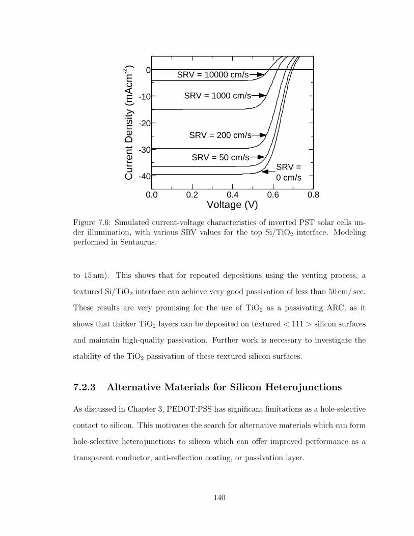
0 . 0 0 . 2 0 . 4 0 . 6 0 . 8- 4 0
- 3 0
- 2 0
- 1 0
0
Curre
nt De
nsity
(mAc
m-2 )
V o l t a g e ( V )
S R V = 0 c m / s
S R V = 5 0 c m / s
S R V = 2 0 0 c m / s
S R V = 1 0 0 0 c m / sS R V = 1 0 0 0 0 c m / s
Figure 7.6: Simulated current-voltage characteristics of inverted PST solar cells un-der illumination, with various SRV values for the top Si/TiO2 interface. Modelingperformed in Sentaurus.
to 15 nm). This shows that for repeated depositions using the venting process, a
textured Si/TiO2 interface can achieve very good passivation of less than 50 cm/ sec.
These results are very promising for the use of TiO2 as a passivating ARC, as it
shows that thicker TiO2 layers can be deposited on textured < 111 > silicon surfaces
and maintain high-quality passivation. Further work is necessary to investigate the
stability of the TiO2 passivation of these textured silicon surfaces.
7.2.3 Alternative Materials for Silicon Heterojunctions
As discussed in Chapter 3, PEDOT:PSS has significant limitations as a hole-selective
contact to silicon. This motivates the search for alternative materials which can form
hole-selective heterojunctions to silicon which can offer improved performance as a
transparent conductor, anti-reflection coating, or passivation layer.
140

1 E + 1 5 1 E + 1 601 02 03 04 05 06 07 08 09 0
1 0 0
SRV (
cm/s)
M i n o r i t y C a r r i e r D e n s i t y ( c m - 3 )1 0 0
2 0 0
3 0 0
4 0 0
5 0 0
Mino
rity Ca
rrier L
ifetim
e (µs
)
Figure 7.7: Surface recombination velocity (filled circles, left axis) and minority carrierlifetime (hollow circles, right axis) vs minority carrier density for a textured float zonesilicon wafer with thick TiO2 deposition.
To this end, some interest has been directed at finding metal oxides which can
form hole-contacts to silicon. Nickel oxide may be suitable, due to the location of
its valence and conduction band relative to those of silicon [52,168,169], however no
such heterojunction has been demonstrated to date. MoO3 has received significant
interest as a high-work-function contact for silicon photovoltaics [170]. MoO3 contacts
with amorphous silicon passivation layers and heterojunction contacts (deposited by
PECVD) have been demonstrated to achieve very high conversion efficiencies [171],
most recently reaching 22.5 % [172]. While these results are promising, ideally such
devices would not require PECVD to deposit the passivation layer. Recent work has
demonstrated the transition metal oxides MoO3, WO3, and V2O5 as hole contacts
directly on n-type silicon [173]. In summary, there are several promising metal oxide
candidates for replacing PEDOT:PSS as a hole selective contact to silicon. Further
141

research regarding these materials on crystalline silicon promises to be an exciting
avenue for future work in this field.
142

Appendix A
Processing Notes
A.1 Top Metal Grid Designs
950 μm
2 mm
200 μm
Figure A.1: 5.4 % area coverage design for top metal grid.
143

515 μm
2 mm
200 μm
Figure A.2: 9.7 % area coverage design for top metal grid.
250 μm
2 mm
200 μm
Figure A.3: 16.2 % area coverage design for top metal grid.
A.2 Parasitic Back Contacts
In conventional silicon solar cells, ohmic contacts are formed by heavily doping the
contact regions by diffusion. However, part of the motivation for low-temperature het-
erojunction solar cells is to eliminate such high-temperature processing steps. There-
144

fore, in fabricating Si/PEDOT:PSS solar cells, care must be taken in order to avoid
the formation of parasitic Schottky barriers at metal-silicon contact regions. The par-
asitic barrier forms due to Fermi-level pinning at the silicon-cathode interface (despite
the choice of a nominally low work-function metal such as aluminum). The effect of
a parasitic Schottky barrier at the rear interface of a solar cell can be described by a
modified Ebers-Moll model as described by Green et. al and others [174–176]. An cir-
cuit diagram of the model (adapted for an n-type base region) is shown in Figure A.4.
IF0IFphotoV
_
+
I
RSh IR0αFIF
αRIR
IRphoto
IF
IR
Figure A.4: Modified Ebers-Moll equivalent circuit for a SOH solar cell [174].
In Figure A.4, there are two diodes which represent the front (Si/PEDOT:PSS)
and rear (parasitic Schottky) junctions formed in the device. IF0 and IR0 represent
the saturation current of the forward and rear junctions, respectively, with the other
junction shorted. αF represents the injection efficiency of the front junction, and IF
is the current flowing through the front junction. Therefore, the current source at
the rear junction αF IF represents the current due to injected holes that reach the
rear junction (and vice versa for αRIR). This represents the current that will flow as
a result of injected holes reaching the rear junction. Also shown are current sources
145

Cathode(-)
n-SiAnode(+)
PEDOTOhmic contact
Hole injection
(a)
Hole injection
Cathode(-)
n-SiAnode(+)
PEDOT Parasitic Schottky barrier
(b)
Figure A.5: Band diagrams of Si/PEDOT:PSS devices with (A) ohmic contact at thecathode and (B) parasitic Schottky back contact in forward bias in the dark.
which represent the photo-generated current collected by each junction. Finally, RSH
represents the shunt resistance associated with the rear junction (The shunt resistance
for the front junction is assumed to be sufficiently high to neglect).
First, the effect of the rear junction in the dark is considered, in which the two
current sources representing photo-current in Figure A.4 are off. If the injection
efficiency of the front junction αF is high (as is the case high quality silicon solar cells),
the current from the front junction IF flows through the current source αF IF , and no
voltage drop occurs across the rear junction. The physical interpretation of the high
injection efficiency means that the majority of the current from the front junction
is from injected holes that reach the back interface and subsequently recombine.
Whether there is an ohmic or parasitic Schottky contact does not matter, as in either
case the holes are able to recombine at the cathode (Figure A.5a and Figure A.5b).
Under illumination, however, the parasitic barrier can have a effect on the VOC
of the device. The open-circuit voltage generated across the device represented in
Figure A.5b is given by Equation A.1.
VOC =nkT
qln
(IF,photoIF,0
+ 1
)− (αF IF,photo + IR,photo)RSH (A.1)
The first term is the expected open-circuit voltage and the second represents the VOC
loss due to the rear junction. Clearly, if the shunt resistance is reduced to zero (as
146

Front Photocurrent
Cathode(-)
n-SiAnode(+)
PEDOT
PhotocurrentBlocked electron
current
Ohmic contact
(a)
Front Photocurrent
Cathode(-)
n-SiAnode(+)
PEDOT
PhotocurrentVOC loss
Blocked electron current
Parasitic Schottky barrier
(b)
Figure A.6: Band diagrams of Si/PEDOT:PSS devices with (A) ohmic contact at thecathode and (B) parasitic Schottky back contact in forward bias and under illumina-tion, showing VOC loss.
in a good ohmic contact), then the loss of VOC will reduced to zero as well. However
if RSH is non-negligible, then the loss of VOC will scale with the photocurrent. The
VOC loss depends on the front junction photocurrent IF,photo and injection efficiency
αF because as the front junction collects a photogenerated hole, the n-type substrate
becomes negatively charged. Similarly, the rear Schottky junction will collect some
amount of photogenerated holes which causes the substrate to become negatively
charged. However, electrons are prevented from leaving via the front of the device
due to the electron blocker (or the p+-n junction of a conventional device), and
therefore must leave via the rear junction. If the rear contact is ohmic, the electrons
are free to reach the cathode, but if a Schottky barrier exists here, then it must be
forward biased in order to allow the electrons to escape. This results in a voltage drop
between the n-Si substrate and the cathode, and a lower VOC as measured measured
between the anode and cathode of the device. This is illustrated in Figure A.6a for a
device with an ohmic contact and Figure A.6b for a device with a parasitic Schottky
contact.
The effect of the parasitic backside contact was observed primarily for double-
side polished n-type substrates. Evaporating the aluminum cathode directly onto a
polished n-type silicon surface resulted in a parasitic back contact. This effect was
147

0 . 3 0 . 4 0 . 5 0 . 6
1 0 - 5
1 0 - 4
1 0 - 3
1 0 - 2
Curre
nt De
nsity
(Acm-2 )
V o l t a g e ( V )
U n s c r i b e dS c r i b e d
(a)
- 0 . 4 - 0 . 2 0 . 0 0 . 2 0 . 4 0 . 6 0 . 8- 4 0- 3 0- 2 0- 1 0
01 02 03 04 0
Curre
nt De
nsity
(mAc
m-2 )
V o l t a g e ( V )
S c r i b e d
U n s c r i b e d
(b)
Figure A.7: Current-density vs voltage characteristics of PEDOT/Si devices with(filled circles) and without (hollow circles) backside scribing. (A) A semi-log plot inthe dark and (B) a linear plot under AM1.5G illumination.
observed to be mitigated by roughening the back (cathode side) surface of the silicon
by diamond scribing prior to aluminum evaporation.
Figure A.7a shows the zoomed in view of the dark current of two Si/PEDOT:PSS
devices, with and without scribing of the silicon before aluminum cathode evapora-
tion. There is no distinguishable difference between the dark current J-V character-
istics of the two devices. This is consistent with the physical picture presented in
Figures A.5a and A.5b which show that the parasitic Schottky barrier will not have
an effect on the dark current compared to a device with an ohmic contact.
Figure A.7b shows the current-voltage characteristics of the same two devices
under illumination. The device without backside scribing exhibits a low VOC of , in
contrast to the achieved by the scribed device. The loss of VOC in the unscribed device
is attributed to formation of a parasitic Schottky barrier as discussed. Introducing
damage intentionally via scribing of the backside helps produce shunt paths [177] at
the aluminum silicon interface, which allow electron current to bypass the Schottky
barrier.
148

Appendix B
List of Publications
B.1 Journal publications
1. “A 12 % efficient silicon/PEDOT: PSS heterojunction solar cell fabricated at
100 C.” Ken A. Nagamatsu, Sushobhan Avasthi, Janam Jhaveri, and James
C. Sturm, Photovoltaics, IEEE Journal of 4.1 (2014): 260-264.
2. “Titanium dioxide/silicon hole-blocking selective contact to enable double-
heterojunction crystalline silicon-based solar cell.” Ken A. Nagamatsu,
Sushobhan Avasthi, Girija Sahasrabudhe, Gabriel Man, Janam Jhaveri,
Alexander H. Berg, Jeffrey Schwartz, Antoine Kahn, Sigurd Wagner, James C.
Sturm, Applied Physics Letters 106.12 (2015): 123906.
3. “Improved efficiency of hybrid organic photovoltaics by pulsed laser sintering
of silver nanowire network transparent electrode.” Joshua A. Spechler, Ken
A. Nagamatsu, James C. Sturm, Craig B. Arnold, ACS applied materials &
interfaces (2015).
149

B.2 Conference Proceedings, Presentations, and
Posters
1. “Current Mechanisms in Silicon-organic Heterojunction Solar Cells with Trans-
fer Printed Metalization” Ken A. Nagamatsu, Joshua Spechler, Sushobhan
Avasthi, Craig Arnold, James C. Sturm, presented at 2012 Materials Research
Society Fall Meeting November 25-30, 2012 Boston, MA
2. “High-Conductivity, High-Transparency PEDOT Films by Direct Application
of Silver Nanowires on 10.6 % Low Temperature Hybrid Photovoltaic Device.”
Ken A. Nagamatsu, Joshua Spechler, Sushobhan Avasthi, Craig Arnold, and
James C. Sturm, poster presented at 2013 Materials Research Society Spring
Meeting April 1-5, (2013) San Francisco, CA
3. “Integrated laser processed silver nanowire transparent electrodes with organic
electronic devices.” Joshua Spechler, Ken A. Nagamatsu, James C. Sturm, and
Craig B. Arnold, CLEO: Science and Innovations. Optical Society of America,
(2013).
4. “Hole-blocking crystalline-silicon/titanium-oxide heterojunction with very low
interface recombination velocity.” Janam Jhaveri, Sushobhan Avasthi, Gabriel
Man, William E. McClain, Ken A. Nagamatsu, Antoine Kahn, Jeffrey Schwartz,
and James C. Sturm. In Photovoltaic Specialists Conference (PVSC), 2013
IEEE 39th, pp. 3292-3296. IEEE, (2013).
5. ”Wide bandgap HBT on crystalline silicon using electron-blocking PEDOT: PSS
emitter.” Janam Jhaveri, Sushobhan Avasthi, Ken A. Nagamatsu, and James
C. Sturm, In Device Research Conference (DRC), 2013 71st Annual, pp. 77-78.
IEEE, (2013).
150

6. “Wide Bandgap Heterojunctions on Crystalline Silicon.” James C. Sturm,
Sushobhan Avasthi, Ken A. Nagamatsu, Janam Jhaveri, William E. McClain,
Gabriel Man, Antoine Kahn, Jeffrey Schwartz, and Sigurd Wagner ECS Trans-
actions 58, no. 9 (2013): 97-105. Invited
7. “Hole-Blocking Metal-Oxide/Crystalline-Silicon Heterojunctions with Recom-
bination Velocity of <100 cm/s.” Sushobhan Avasthi, William E. McClain,
Yasmin Afsar, Gabriel Man, Janam Jhaveri, Ken A. Nagamatsu, Antoine Kahn,
Jeffrey Schwartz, Sigurd Wagner, and James C. Sturm, presented at 2014 Ma-
terials Research Society Spring Meeting April 21-25, 2014 San Francisco, CA.
Invited
8. “Growth Mechanism and Carrier Transport in Hole-Blocking TiO2/Silicon Het-
erojunctions” Sushobhan Avasthi, William E. McClain, Gabriel Man, Janam
Jhaveri, Ken A. Nagamatsu, Antoine Kahn, Jeffrey Schwartz, and James C.
Sturm, poster presented at 2013 Materials Research Society Spring Meeting
April 21-25, 2013 San Francisco, CA
9. “Silicon/Organic Heterojunction Photovoltaic Cell with 12.7 % Efficiency by
Use of Spray-Coated Nanowire Transparent Conductor” Ken A. Nagamatsu,
Joshua Spechler, Sushobhan Avasthi, Craig Arnold, James C. Sturm, presented
at 2013 Materials Research Society Spring Meeting April 21-25, 2013 San Fran-
cisco, CA
10. “Stable low-recombination n-Si/TiO 2 hole-blocking interface and its effect on
silicon heterojunction photovoltaics.” Janam Jhaveri, Sushobhan Avasthi, Ken
A. Nagamatsu, and James C. Sturm, In Photovoltaic Specialist Conference
(PVSC), 2014 IEEE 40th, pp. 1525-1528. IEEE, (2014).
151

11. “Double-heterojunction crystalline silicon solar cell fabricated at 250 C with
12.9 % efficiency.” Sushobhan Avasthi, Ken A. Nagamatsu, Janam Jhaveri,
William E. McClain, Gabriel Man, Antoine Kahn, Jeffrey Schwartz, Sigurd
Wagner, and James C. Sturm, In Photovoltaic Specialist Conference (PVSC),
2014 IEEE 40th, pp. 0949-0952. IEEE, (2014).
12. “Effect of Annealing on Stability of Low Interface Recombination Velocity at
TiO2/p-Silicon Interface.” Janam Jhaveri, Sushobhan Avasthi, Gabriel Man,
Ken A. Nagamatsu, William E. McClain, Jeffrey Schwartz, Antoine Kahn, and
James C. Sturm, presented at 2013 Materials Research Society Spring Meeting
April 21-25, 2014 San Francisco, CA
13. “Double-heterojunction crystalline silicon solar cell with electron-selective
TiO2 cathode contact fabricated at 100C with open-circuit voltage of 640
mV.”Janam Jhaveri, Ken A. Nagamatsu, Alexander H. Berg, Gabriel Man,
Girija Sahasrabudhe, Sigurd Wagner, Jeffrey Schwartz, Antoine Kahn, and
James C. Sturm, In Photovoltaic Specialist Conference (PVSC), 2015 IEEE
42nd IEEE, (2015).
152

Bibliography
[1] R.K. Pachauri Core Writing Team and L.A. Meyer (eds.). IPCC, 2014: ClimateChange 2014: Synthesis Report. Contribution of Working Groups I, II and IIIto the Fifth Assessment Report of the Intergovernmental Panel on ClimateChange. Technical report, IPCC, Geneva, Switzerland, 2014.
[2] Department of Economic United Nations and Population Division Social Affairs.World Population Prospects: The 2015 Revision. http://tools.ietf.org/
html/rfc5246, 2015.
[3] David MacKay. Sustainable Energy-without the hot air. UIT Cambridge, 2008.
[4] Mark J. Kerr and Andres Cuevas. General parameterization of Auger recombi-nation in crystalline silicon. Journal of Applied Physics, 91(4):2473, 2002.
[5] We Shockley and WT Read Jr. Statistics of the recombinations of holes andelectrons. Physical review, 87(5):835, 1952.
[6] Re N Hall. Electron-hole recombination in germanium. Physical Review,87(2):387, 1952.
[7] A. B. Sproul. Dimensionless solution of the equation describing the effect ofsurface recombination on carrier decay in semiconductors. Journal of AppliedPhysics, 76(5):2851, 1994.
[8] Kenneth E Bean et al. Anisotropic etching of silicon. IEEE Transactions onElectron Devices, 25(10):1185–1193, 1978.
[9] H Seidel, L Csepregi, A Heuberger, and H Baumgartel. Anisotropic etching ofcrystalline silicon in alkaline solutions i. orientation dependence and behaviorof passivation layers. Journal of the electrochemical society, 137(11):3612–3626,1990.
[10] Osamu Tabata, Ryouji Asahi, Hirofumi Funabashi, Keiichi Shimaoka, andSusumu Sugiyama. Anisotropic etching of silicon in tmah solutions. Sensorsand Actuators A: Physical, 34(1):51–57, 1992.
[11] Martin A. Green, Keith Emery, Yoshihiro Hishikawa, Wilhelm Warta, andEwan D. Dunlop. Solar cell efficiency tables (Version 45). Progress in Pho-tovoltaics: Research and Applications, 23(1):1–9, January 2015.
153

[12] Jianhua Zhao, Aihua Wang, Martin a. Green, and Francesca Ferrazza. 19.8%efficient honeycomb textured multicrystalline and 24.4% monocrystalline siliconsolar cells. Applied Physics Letters, 73(14):1991, 1998.
[13] Peter J. Cousins, David D. Smith, Hsin-Chiao Luan, Jane Manning, Tim D.Dennis, Ann Waldhauer, Karen E. Wilson, Gabriel Harley, and William P.Mulligan. Generation 3: Improved performance at lower cost. In 2010 35thIEEE Photovoltaic Specialists Conference, pages 000275–000278. IEEE, June2010.
[14] J. Zhao, A. Wang, P. Altermatt, and M. a. Green. Twenty-four percent efficientsilicon solar cells with double layer antireflection coatings and reduced resistanceloss. Applied Physics Letters, 66(26):3636, 1995.
[15] Martin A Green. Solar cells: operating principles, technology, and system ap-plications. Prentice-Hall, Inc., Englewood Cliffs, NJ, 1982.
[16] Jenny Nelson. The physics of solar cells, volume 1. World Scientific, 2003.
[17] Alan Goodrich, Peter Hacke, Qi Wang, Bhushan Sopori, Robert Margolis,Ted L. James, and Michael Woodhouse. A wafer-based monocrystalline siliconphotovoltaics road map: Utilizing known technology improvement opportuni-ties for further reductions in manufacturing costs. Solar Energy Materials andSolar Cells, 114:110–135, jul 2013.
[18] M.A. Green. Limits on the open-circuit voltage and efficiency of silicon solarcells imposed by intrinsic Auger processes. IEEE Transactions on ElectronDevices, 31(5):671–678, may 1984.
[19] M.J. Kerr, P. Campbell, and Andres Cuevas. Lifetime and efficiency limits ofcrystalline silicon solar cells. In Conference Record of the Twenty-Ninth IEEEPhotovoltaic Specialists Conference, 2002., pages 438–441. IEEE, 2002.
[20] JG Fossum, FA Lindholm, and MA Shibib. The importance of surface recom-bination and energy-bandgap arrowing in p-n-junction silicon solar cells. IEEETransactions on Electron Devices, 26(9):1294–1298, sep 1979.
[21] R.M. Swanson. Approaching the 29% limit efficiency of silicon solar cells. InConference Record of the Thirty-first IEEE Photovoltaic Specialists Conference,2005., pages 889–894. IEEE, 2005.
[22] Sushobhan Avasthi, Stephanie Lee, Yueh-Lin Loo, and James C Sturm. Roleof majority and minority carrier barriers silicon/organic hybrid heterojunctionsolar cells. Advanced materials, 23(48):5762–5766, December 2011.
[23] Sushobhan Avasthi. Crystalline-Silicon/Organic Heterojunctions for Solar Pho-tovoltaics. PhD thesis, Princeton University, 2011.
154

[24] Sushobhan Avasthi and James C. Sturm. Charge separation and minority car-rier injection in P3HT-silicon heterojunction solar cells. In 2011 37th IEEEPhotovoltaic Specialists Conference, pages 002487–002489. IEEE, June 2011.
[25] E Yablonovitch, T. Gmitter, R M Swanson, and Y H Kwark. A 720 mV opencircuit voltage SiOx:c-Si:SiOx double heterostructure solar cell. Applied PhysicsLetters, 47(11):1211, 1985.
[26] Keiichiro Masuko, Masato Shigematsu, Taiki Hashiguchi, Daisuke Fujishima,Motohide Kai, Naoki Yoshimura, Tsutomu Yamaguchi, Yoshinari Ichihashi,Takahiro Mishima, Naoteru Matsubara, Tsutomu Yamanishi, Tsuyoshi Taka-hama, Mikio Taguchi, Eiji Maruyama, and Shingo Okamoto. Achievement ofMore Than 25 Percent Conversion Efficiency With Crystalline Silicon Hetero-junction Solar Cell. IEEE Journal of Photovoltaics, 4(6):1433–1435, November2014.
[27] R.a. Sinton, A. Cuevas, and M. Stuckings. Quasi-steady-state photoconduc-tance, a new method for solar cell material and device characterization. InConference Record of the Twenty Fifth IEEE Photovoltaic Specialists Confer-ence - 1996, pages 457–460. IEEE, 1996.
[28] Tracey M. Clarke and James R. Durrant. Charge Photogeneration in OrganicSolar Cells. Chemical Reviews, 110(11):6736–6767, November 2010.
[29] Martin a. Green. Improved value for the silicon free exciton binding energy.AIP Advances, 3(11):112104, 2013.
[30] Sushobhan Avasthi, Yabing Qi, Grigory K. Vertelov, Jeffrey Schwartz, AntoineKahn, and James C. Sturm. Silicon surface passivation by an organic overlayerof 9,10-phenanthrenequinone. Applied Physics Letters, 96(22):222109, 2010.
[31] V Srikant and D. R. Clarke. On the optical band gap of zinc oxide. Journal ofApplied Physics, 83(10):5447, 1998.
[32] L. Kavan, M. Gratzel, S. E. Gilbert, C. Klemenz, and H. J. Scheel. Electrochem-ical and Photoelectrochemical Investigation of Single-Crystal Anatase. Journalof the American Chemical Society, 118(28):6716–6723, January 1996.
[33] Ruiyuan Liu, Shuit-Tong Lee, and Baoquan Sun. 13.8% Efficiency HybridSi/Organic Heterojunction Solar Cells with MoO 3 Film as Antireflection andInversion Induced Layer. Advanced Materials, 2, 2014.
[34] Ulrike Diebold. The surface science of titanium dioxide. Surface Science Re-ports, 48(5-8):53–229, January 2003.
[35] B. Hoex, J. Schmidt, P. Pohl, M. C. M. van de Sanden, and W. M. M. Kessels.Silicon surface passivation by atomic layer deposited Al2O3. Journal of AppliedPhysics, 104(4):044903, 2008.
155

[36] B. Hoex, S. B S Heil, E. Langereis, M. C. M. van de Sanden, and W. M MKessels. Ultralow surface recombination of c-Si substrates passivated by plasma-assisted atomic layer deposited Al[sub 2]O[sub 3]. Applied Physics Letters,89(4):042112, 2006.
[37] G. Dingemans, P. Engelhart, R. Seguin, F. Einsele, B. Hoex, M. C. M. van deSanden, and W. M. M. Kessels. Stability of Al2O3 and Al2O3/a-SiNx:Hstacks for surface passivation of crystalline silicon. Journal of Applied Physics,106(11):114907, 2009.
[38] G. Dingemans and W. M. M. Kessels. Status and prospects of Al2O3-basedsurface passivation schemes for silicon solar cells. Journal of Vacuum Science& Technology A: Vacuum, Surfaces, and Films, 30(4):040802, 2012.
[39] Sushobhan Avasthi, William E McClain, Gabriel Man, Antoine Kahn, Jef-frey Schwartz, and James C Sturm. Hole-blocking titanium-oxide/silicon het-erojunction and its application to photovoltaics. Applied Physics Letters,102(20):203901, 2013.
[40] Makoto Tanaka, Mikio Taguchi, Takao Matsuyama, Toru Sawada, ShinyaTsuda, Shoichi Nakano, Hiroshi Hanafusa, and Yukinori Kuwano. Develop-ment of new a-si/c-si heterojunction solar cells: Acj-hit (artificially constructedjunction-heterojunction with intrinsic thin-layer). Japanese Journal of AppliedPhysics, 31(11R):3518, 1992.
[41] G. D. Cody, T. Tiedje, B. Abeles, B. Brooks, and Y. Goldstein. Disorder andthe Optical-Absorption Edge of Hydrogenated Amorphous Silicon. PhysicalReview Letters, 47(20):1480–1483, nov 1981.
[42] Hideharu Matsuura, Tetsuhiro Okuno, Hideyo Okushi, and Kazunobu Tanaka.Electrical properties of n-amorphous/p-crystalline silicon heterojunctions. Jour-nal of Applied Physics, 55(4):1012, 1984.
[43] Mikio Taguchi, Akira Terakawa, Eiji Maruyama, and Makoto Tanaka. Ob-taining a Higher Voc in HIT cells. Progress in Photovoltaics: Research andApplications, 13(6):481–488, sep 2005.
[44] J.E. Cotter, J.H. Guo, P.J. Cousins, M.D. Abbott, F.W. Chen, and K.C. Fisher.P-Type Versus n-Type Silicon Wafers: Prospects for High-Efficiency Commer-cial Silicon Solar Cells. IEEE Transactions on Electron Devices, 53(8):1893–1901, aug 2006.
[45] Mikio Taguchi, Ayumu Yano, Satoshi Tohoda, Kenta Matsuyama, Yuya Naka-mura, Takeshi Nishiwaki, Kazunori Fujita, and Eiji Maruyama. 24.7% Recordefficiency HIT solar cell on thin silicon wafer. IEEE Journal of Photovoltaics,4(1):96–99, 2014.
156

[46] Andreas Elschner, Stephan Kirchmeyer, Wilfried Lovenich, Udo Merker, andKnud Reuter. PEDOT: principles and applications of an intrinsically conductivepolymer. CRC Press, 2010.
[47] Desalegn Alemu, Hung-Yu Wei, Kuo-Chuan Ho, and Chih-Wei Chu. Highlyconductive PEDOT:PSS electrode by simple film treatment with methanol forITO-free polymer solar cells. Energy & Environmental Science, 5(11):9662,2012.
[48] Hung Do, Manuel Reinhard, Henry Vogeler, Andreas Puetz, Michael F.G. Klein,Wilhelm Schabel, Alexander Colsmann, and Uli Lemmer. Polymeric anodesfrom poly(3,4-ethylenedioxythiophene):poly(styrenesulfonate) for 3.5% efficientorganic solar cells. Thin Solid Films, 517(20):5900–5902, August 2009.
[49] Seok-In Na, Seok-Soon Kim, Jang Jo, and Dong-Yu Kim. Efficient and Flex-ible ITO-Free Organic Solar Cells Using Highly Conductive Polymer Anodes.Advanced Materials, 20(21):4061–4067, November 2008.
[50] L. Groenendaal, Friedrich Jonas, Dieter Freitag, Harald Pielartzik, and John RReynolds. Poly(3,4-ethylenedioxythiophene) and Its Derivatives: Past, Present,and Future. Advanced Materials, 12(7):481–494, April 2000.
[51] Jaehyung Hwang, Fabrice Amy, and Antoine Kahn. Spectroscopic study onsputtered PEDOT:PSS: Role of surface PSS layer. Organic Electronics: physics,materials, applications, 7(5):387–396, 2006.
[52] Erin L. Ratcliff, Jens Meyer, K. Xerxes Steirer, Neal R. Armstrong, Dana Olson,and Antoine Kahn. Energy level alignment in PCDTBT:PC70BM solar cells:Solution processed NiOx for improved hole collection and efficiency. OrganicElectronics, 13(5):744–749, may 2012.
[53] Andreas Elschner and Wilfried Lovenich. Solution-deposited PEDOT for trans-parent conductive applications. MRS Bulletin, 36(10):794–798, October 2011.
[54] Ken A Nagamatsu, Sushobhan Avasthi, Janam Jhaveri, and James C Sturm.A 12% Efficient Silicon/PEDOT:PSS Heterojunction Solar Cell Fabricated at ¡100 C. IEEE Journal of Photovoltaics, 4(1):260–264, jan 2014.
[55] Qiming Liu, Masahiro Ono, Zeguo Tang, Ryo Ishikawa, Keiji Ueno, and HajimeShirai. Highly efficient crystalline silicon/Zonyl fluorosurfactant-treated organicheterojunction solar cells. Applied Physics Letters, 100(18):183901, 2012.
[56] Ann S. Erickson, Arava Zohar, and David Cahen. n-Si-Organic Inversion LayerInterfaces: A Low Temperature Deposition Method for Forming a p-n Homo-junction in n-Si. Advanced Energy Materials, 4(9):1301724, June 2014.
[57] Sangmoo Jeong, Erik C Garnett, Shuang Wang, Zongfu Yu, Shanhui Fan,Mark L Brongersma, Michael D McGehee, and Yi Cui. Hybrid silicon nanocone-polymer solar cells. Nano letters, 12(6):2971–6, June 2012.
157

[58] Ting-Gang Chen, Bo-Yu Huang, En-Chen Chen, Peichen Yu, and Hsin-FeiMeng. Micro-textured conductive polymer/silicon heterojunction photovoltaicdevices with high efficiency. Applied Physics Letters, 101(3):033301, 2012.
[59] Yunfang Zhang, Fengshuo Zu, Shuit-Tong Lee, Liangsheng Liao, Ni Zhao, andBaoquan Sun. Heterojunction with Organic Thin Layers on Silicon for RecordEfficiency Hybrid Solar Cells. Advanced Energy Materials, 4(2), January 2014.
[60] Yunfang Zhang, Wei Cui, Yawen Zhu, Fengshuo Zu, Liangsheng Liao,Shuit-Tong Lee, and Baoquan Sun. High efficiency hybrid PE-DOT:PSS/nanostructured silicon Schottky junction solar cells by doping-freerear contact. Energy Environ. Sci., 8:297–302, 2015.
[61] Sara Jackle, Matthias Mattiza, Martin Liebhaber, Gerald Bronstrup, MathiasRommel, Klaus Lips, and Silke Christiansen. Junction formation and currenttransport mechanisms in hybrid n-Si/PEDOT:PSS solar cells. Scientific Re-ports, 5:13008, August 2015.
[62] Werner Kern and J Electrochem Soc. The Evolution of Silicon Wafer CleaningTechnology. Journal of the Electrochemical Society, 137(6):1887–1892, 1990.
[63] M. Grundner and H. Jacob. Investigations on hydrophilic and hydrophobicsilicon (100) wafer surfaces by X-ray photoelectron and high-resolution electronenergy loss-spectroscopy. Applied Physics A Solids and Surfaces, 39(2):73–82,February 1986.
[64] Takumi Takano, Hiroyasu Masunaga, Akihiko Fujiwara, Hidenori Okuzaki, andTakahiko Sasaki. PEDOT Nanocrystal in Highly Conductive PEDOT:PSS Poly-mer Films. Macromolecules, 45(9):3859–3865, May 2012.
[65] Thomas Stocker, Anna Kohler, and Ralf Moos. Why does the electrical con-ductivity in PEDOT:PSS decrease with PSS content? A study combining ther-moelectric measurements with impedance spectroscopy. Journal of PolymerScience, Part B: Polymer Physics, 50(14):976–983, 2012.
[66] A. M. Nardes, M. Kemerink, R. A. J. Janssen, J. A. M. Bastiaansen, N. M. M.Kiggen, B. M. W. Langeveld, A. J. J. M. van Breemen, and M. M. de Kok.Microscopic Understanding of the Anisotropic Conductivity of PEDOT:PSSThin Films. Advanced Materials, 19(9):1196–1200, May 2007.
[67] Cristian Ionescu-Zanetti, Adam Mechler, Sue A Carter, and Ratnesh Lal. Semi-conductive polymer blends: correlating structure with transport properties atthe nanoscale. Advanced Materials, 16(5):385–389, 2004.
[68] a.M. Nardes, M. Kemerink, M.M. de Kok, E. Vinken, K. Maturova, and R.a.J.Janssen. Conductivity, work function, and environmental stability of PE-DOT:PSS thin films treated with sorbitol. Organic Electronics, 9(5):727–734,October 2008.
158

[69] X Crispin, F L E Jakobsson, A Crispin, P C M Grim, P Anders-son, A Volodin, C Van Haesendonck, M Van Der Auweraer, W R Sala-neck, and M Berggren. The Origin of the High Conductivity of Poly(3,4-ethylenedioxythiophene)Poly(styrenesulfonate) (PEDOT - PSS) Plastic Elec-trodes. Chemistry of Materials, 18(18):4354–4360, 2006.
[70] Jianyong Ouyang, Qianfei Xu, Chi Wei Chu, Yang Yang, Gang Li, and JosephShinar. On the mechanism of conductivity enhancement in poly(3,4- ethylene-dioxythiophene):poly(styrene sulfonate) film through solvent treatment. Poly-mer, 45(25):8443–8450, 2004.
[71] Seok-In Na, Gunuk Wang, Seok-Soon Kim, Tae-Wook Kim, Seung-Hwan Oh,Byung-Kwan Yu, Takhee Lee, and Dong-Yu Kim. Evolution of nanomor-phology and anisotropic conductivity in solvent-modified PEDOT:PSS filmsfor polymeric anodes of polymer solar cells. Journal of Materials Chemistry,19(47):9045, 2009.
[72] Jacek Gasiorowski, Reghu Menon, Kurt Hingerl, Marko Dachev, and Niyazi Ser-dar Sariciftci. Surface morphology, optical properties and conductivity changesof poly(3,4-ethylenedioxythiophene):poly(styrenesulfonate) by using additives.Thin Solid Films, 536(100):211–215, June 2013.
[73] J.Y. Kim, J.H. Jung, D.E. Lee, and J Joo. Enhancement of electrical conductiv-ity of poly(3,4-ethylenedioxythiophene)/poly(4-styrenesulfonate) by a change ofsolvents. Synthetic Metals, 126(2-3):311–316, February 2002.
[74] Michael Vosgueritchian, Darren J. Lipomi, and Zhenan Bao. Highly Conduc-tive and Transparent PEDOT:PSS Films with a Fluorosurfactant for Stretch-able and Flexible Transparent Electrodes. Advanced Functional Materials,22(2):421–428, January 2012.
[75] S.K.M Jonsson, J Birgerson, X Crispin, G Greczynski, W Osikowicz,A.W Denier van der Gon, W.R Salaneck, and M Fahlman. The ef-fects of solvents on the morphology and sheet resistance in poly(3,4-ethylenedioxythiophene)polystyrenesulfonic acid (PEDOTPSS) films. SyntheticMetals, 139(1):1–10, August 2003.
[76] Yijie Xia, Kuan Sun, and Jianyong Ouyang. Solution-Processed Metallic Con-ducting Polymer Films as Transparent Electrode of Optoelectronic Devices.Advanced Materials, 24(18):2436–2440, May 2012.
[77] J. Tersoff. Schottky Barrier Heights and the Continuum of Gap States. PhysicalReview Letters, 52(6):465–468, February 1984.
[78] A.S. Grove and C.T. Sah. Simple analytical approximations to the switchingtimes in narrow base diodes. Solid-State Electronics, 7(1):107–110, January1964.
159

[79] Robert Kingston. Switching Time in Junction Diodes and Junction Transistors.Proceedings of the IRE, 42(5):829–834, May 1954.
[80] Hansjochen Benda and Eberhard Spenke. Reverse recovery processes in siliconpower rectifiers. Proceedings of the IEEE, 55(8):1331–1354, 1967.
[81] Benjamin Lax and S. F. Neustadter. Transient Response of a p-n Junction.Journal of Applied Physics, 25(9):1148–1154, 1954.
[82] J.J. Liou, H.K. Brown, and M.S. Clamme. Characterization of reverse recoverytransient behavior of bipolar transistors for emitter parameters determination.Solid-State Electronics, 31(11):1595–1601, November 1988.
[83] L.A. Davidson. Simple expression for storage time of arbitrary base diode.Solid-State Electronics, 9(11-12):1145–1147, November 1966.
[84] M. Byczkowski and J. R. Madigan. Minority Carrier Lifetime in p-n JunctionDevices. Journal of Applied Physics, 28(8):878–881, 1957.
[85] R.W. Dutton and R.J. Whittier. Forward Current-Voltage and switching char-acteristics of p+-n-n+(epitaxial) diodes. IEEE Transactions on Electron De-vices, 16(5):458–467, May 1969.
[86] Yun-Ho Kim, Soo-Hyoung Lee, Jaegeun Noh, and Sung-Hwan Han. Per-formance and stability of electroluminescent device with self-assembled lay-ers of poly(3,4-ethylenedioxythiophene)poly(styrenesulfonate) and polyelec-trolytes. Thin Solid Films, 510(1-2):305–310, jul 2006.
[87] Jun Ni, He Yan, Anchuang Wang, Yu Yang, Charlotte L. Stern, Andrew W.Metz, Shu Jin, Lian Wang, Tobin J. Marks, John R. Ireland, and Carl R.Kannewurf. MOCVD-Derived Highly Transparent, Conductive Zinc- and Tin-Doped Indium Oxide Thin Films: Precursor Synthesis, Metastable Phase FilmGrowth and Characterization, and Application as Anodes in Polymer Light-Emitting Diodes. Journal of the American Chemical Society, 127(15):5613–5624, apr 2005.
[88] Keith R. McIntosh and Simeon C. Baker-Finch. OPAL 2: Rapid optical simula-tion of silicon solar cells. In 2012 38th IEEE Photovoltaic Specialists Conference,pages 000265–000271. IEEE, June 2012.
[89] Simeon C. Baker-Finch and Keith R. McIntosh. A freeware program for pre-cise optical analysis of the front surface of a solar cell. In 2010 35th IEEEPhotovoltaic Specialists Conference, pages 002184–002187. IEEE, June 2010.
[90] Simeon C. Baker-Finch and Keith R. McIntosh. Reflection of normally incidentlight from silicon solar cells with pyramidal texture. Progress in Photovoltaics:Research and Applications, 19(4):406–416, June 2011.
160

[91] Simeon C. Baker-Finch and Keith R. McIntosh. Reflection distributions oftextured monocrystalline silicon: implications for silicon solar cells. Progress inPhotovoltaics: Research and Applications, 20(1), March 2012.
[92] Simeon C. Baker-Finch and Keith R. McIntosh. One-dimensional photogener-ation profiles in silicon solar cells with pyramidal texture. Progress in Photo-voltaics: Research and Applications, 20(1):51–61, January 2012.
[93] Simeon C Baker-Finch, Keith R Mcintosh, Mason L Terry, and A HemisphericalReflectance. Isotextured Silicon Solar Cell Analysis and Modeling 1 : Optics.IEEE Journal of Photovoltaics, 2(4):457–464, 2012.
[94] Simeon C Baker-finch, Keith R Mcintosh, Mason L Terry, and A HemisphericalReflectance. Isotextured Silicon Solar Cell Analysis and Modeling 1 : Optics.IEEE Journal of Photovoltaics, 2(4):457–464, 2012.
[95] Lining He, Changyun Jiang, Hao Wang, Donny Lai, and Rusli. High efficiencyplanar Si/organic heterojunction hybrid solar cells. Applied Physics Letters,100(7), 2012.
[96] Jan Schmidt, Valeriya Titova, and Dimitri Zielke. Organic-silicon heterojunc-tion solar cells: Open-circuit voltage potential and stability. Applied PhysicsLetters, 103(18), 2013.
[97] Karsten Schilling, Bobbie Bradford, Dominique Castelli, Eric Dufour, J FrankNash, Wolfgang Pape, Stefan Schulte, Ian Tooley, Jeroen van den Bosch, andFlorian Schellauf. Human safety review of nano titanium dioxide and zinc oxide.Photochemical & Photobiological Sciences, 9(4):495, 2010.
[98] Akira Fujishima and Kenichi Honda. Electrochemical Photolysis of Water at aSemiconductor Electrode. Nature, 238(5358):37–38, July 1972.
[99] Akira Fujishima, Tata N. Rao, and Donald a. Tryk. Titanium dioxide pho-tocatalysis. Journal of Photochemistry and Photobiology C: PhotochemistryReviews, 1(1):1–21, June 2000.
[100] Miguel Pelaez, Nicholas T. Nolan, Suresh C. Pillai, Michael K. Seery, PolycarposFalaras, Athanassios G. Kontos, Patrick S.M. Dunlop, Jeremy W.J. Hamilton,J.Anthony Byrne, Kevin O’Shea, Mohammad H. Entezari, and Dionysios D.Dionysiou. A review on the visible light active titanium dioxide photocatalystsfor environmental applications. Applied Catalysis B: Environmental, 125:331–349, August 2012.
[101] C. Waldauf, M. Morana, P. Denk, P. Schilinsky, K. Coakley, S. a. Choulis,and C. J. Brabec. Highly efficient inverted organic photovoltaics using solutionbased titanium oxide as electron selective contact. Applied Physics Letters,89(23):233517, 2006.
161

[102] Kai-Lin Ou, Delvin Tadytin, K. Xerxes Steirer, Diogenes Placencia, MikeNguyen, Paul Lee, and Neal R. Armstrong. Titanium dioxide electron-selectiveinterlayers created by chemical vapor deposition for inverted configuration or-ganic solar cells. Journal of Materials Chemistry A, 1(23):6794, May 2013.
[103] Sung Heum Park, Anshuman Roy, Serge Beaupre, Shinuk Cho, Nelson Coates,Ji Sun Moon, Daniel Moses, Mario Leclerc, Kwanghee Lee, and Alan J. Heeger.Bulk heterojunction solar cells with internal quantum efficiency approaching100%. Nature Photonics, 3(5):297–302, May 2009.
[104] Julian Burschka, Norman Pellet, Soo-Jin Moon, Robin Humphry-Baker, PengGao, Mohammad K Nazeeruddin, and Michael Gratzel. Sequential deposi-tion as a route to high-performance perovskite-sensitized solar cells. Nature,499(7458):316–319, July 2013.
[105] Jaan Aarik, Aleks Aidla, Teet Uustare, and Vaino Sammelselg. Morphologyand structure of TiO2 thin films grown by atomic layer deposition. Journal ofCrystal Growth, 148(3):268–275, March 1995.
[106] Jaan Aarik, Ateks Aidla, A A Kiisler, Teet Uustare, and V Sammelselg. Effectof crystal structure on optical properties of TiO 2 films grown by atomic layerdeposition. Thin Solid Films, 305:270–273, 1997.
[107] K S Finnie, G Triani, K T Short, D R G Mitchell, D J Attard, J R Bartlett,and C J Barbe. Influence of Si(100) surface pretreatment on the morphology ofTiO2 films grown by atomic layer deposition. Thin Solid Films, 440(1-2):109–116, September 2003.
[108] D R G Mitchell, D J Attard, and G Triani. Transmission electron microscopystudies of atomic layer deposition TiO2 films grown on silicon. Thin Solid Films,441(1-2):85–95, September 2003.
[109] Rungthiwa Methaapanon and Stacey F Bent. Comparative Study of TitaniumDioxide Atomic Layer Deposition on Silicon Dioxide and Hydrogen-TerminatedSilicon. The Journal of Physical Chemistry C, 114(23):10498–10504, June 2010.
[110] G Triani, J.a. Campbell, P J Evans, J Davis, B.a. Latella, and R P Burford.Low temperature atomic layer deposition of titania thin films. Thin Solid Films,518(12):3182–3189, April 2010.
[111] Jolien Dendooven, Sreeprasanth Pulinthanathu Sree, Koen De Keyser, DavyDeduytsche, Johan A. Martens, Karl F. Ludwig, and Christophe Detavernier.In Situ X-ray Fluorescence Measurements During Atomic Layer Deposition:Nucleation and Growth of TiO 2 on Planar Substrates and in NanoporousFilms. The Journal of Physical Chemistry C, 115(14):6605–6610, April 2011.
[112] Seung Youb Lee, Cheolho Jeon, Seok Hwan Kim, Yooseok Kim, Woosung Jung,Ki-Seok An, and Chong-Yun Park. In-situ X-ray Photoemission Spectroscopy
162

Study of Atomic Layer Deposition of TiO$ 2$ on Silicon Substrate. JapaneseJournal of Applied Physics, 51(3R):31102, February 2012.
[113] Qian Tao, Kirsten Overhage, Gregory Jursich, and Christos Takoudis. Onthe initial growth of atomic layer deposited TiO2 films on silicon and coppersurfaces. Thin Solid Films, 520(22):6752–6756, September 2012.
[114] Guangfen Zhou, Jie Ren, and Shaowen Zhang. Initial growth mechanism ofatomic layer deposited titanium dioxide using cyclopentadienyl-type precursor:A density functional theory study. Thin Solid Films, 524:179–184, December2012.
[115] Stephen McDonnell, Roberto C Longo, Oliver Seitz, Josh B Ballard, GregMordi, Don Dick, James H G Owen, John N Randall, Jiyoung Kim, Yves JChabal, Kyeongjae Cho, and Robert M Wallace. Controlling the Atomic LayerDeposition of Titanium Dioxide on Silicon: Dependence on Surface Termina-tion. The Journal of Physical Chemistry C, 117(39):20250–20259, October 2013.
[116] Elmira Memarzadeh Lotfabad, Peter Kalisvaart, Kai Cui, Alireza Kohande-hghan, Martin Kupsta, Brian Olsen, and David Mitlin. ALD TiO2 coatedsilicon nanowires for lithium ion battery anodes with enhanced cycling stabilityand coulombic efficiency. Physical Chemistry Chemical Physics, 15(32):13646,August 2013.
[117] Baochen Liao, Bram Hoex, Armin G. Aberle, Dongzhi Chi, and Charanjit S.Bhatia. Excellent c-Si surface passivation by low-temperature atomic layerdeposited titanium oxide. Applied Physics Letters, 104(25):253903, June 2014.
[118] Liang Tian, Adurey Soum-Glaude, Fabien Volpi, Luc Salvo, Gregory Berthome,Stephane Coindeau, Arnaud Mantoux, Raphael Boichot, Sabine Lay, VirginieBrize, Elisabeth Blanquet, Gael Giusti, and Daniel Bellet. Undoped TiO2 andnitrogen-doped TiO2 thin films deposited by atomic layer deposition on planarand architectured surfaces for photovoltaic applications. Journal of VacuumScience & Technology A: Vacuum, Surfaces, and Films, 141, 2015.
[119] a. Monoy, a. Brevet, L Imhoff, B Domenichini, E Lesniewska, P M Peterle, M CMarco de Lucas, and S Bourgeois. Surface preparation influence on the initialstages of MOCVD growth of TiO2 thin films. Thin Solid Films, 515(2):687–690,October 2006.
[120] C. Jimenez, D. De Barros, A. Darraz, J.-L. Deschanvres, L. Rapenne, P. Chau-douet, J.E. Mendez, F. Weiss, M. Thomachot, T. Sindzingre, G. Berthome, andF.J. Ferrer. Deposition of TiO2 thin films by atmospheric plasma post-dischargeassisted injection MOCVD. Surface and Coatings Technology, 201(22-23):8971–8975, September 2007.
[121] Reji Thomas, Raghunandan Bhakta, Peter Ehrhart, Roland a. Fischer, RainerWaser, and Anjana Devi. Liquid injection MOCVD of TiO2 and SrTiO3
163

thin films from [Ti(OPri)2(tbaoac)2]: Film properties and compatibility with[Sr(thd)2]. Surface and Coatings Technology, 201(22-23):9135–9140, September2007.
[122] a. Brevet, L Imhoff, M C Marco de Lucas, B Domenichini, and S Bourgeois.Angle resolved X-ray photoemission spectroscopy double layer model for in situcharacterization of metal organic chemical vapour deposition nanometric films.Thin Solid Films, 515(16):6407–6410, June 2007.
[123] B.-C. Kang, D.-Y. Jung, R.a. Fischer, and J.-H. Boo. Selective MOCVD oftitanium oxide and zirconium oxide thin films using single molecular precursorson Si(100) substrates. Journal of Physics and Chemistry of Solids, 69(1):128–132, January 2008.
[124] H.J. Frenck, W Kulisch, M Kuhr, and R Kassing. Deposition of TiO2 thin filmsby plasma-enhanced decomposition of tetraisopropyltitanate. Thin Solid Films,201(2):327–335, June 1991.
[125] Won Gyu Lee, Seong Ihl Woo, Jong Choul Kim, Soo Han Choi, and Kye HwanOh. Preparation and properties of amorphous TiO2 thin films by plasma en-hanced chemical vapor deposition. Thin Solid Films, 237(1-2):105–111, January1994.
[126] Wenli Yang and Colin a. Wolden. Plasma-enhanced chemical vapor depositionof TiO2 thin films for dielectric applications. Thin Solid Films, 515(4):1708–1713, December 2006.
[127] D Li, M Carette, A Granier, J P Landesman, and A Goullet. Spectroscopicellipsometry analysis of TiO2 films deposited by plasma enhanced chemical va-por deposition in oxygen/titanium tetraisopropoxide plasma. Thin Solid Films,522:366–371, November 2012.
[128] D Li, M Carette, A Granier, J P Landesman, and A Goullet. In situ spectro-scopic ellipsometry study of TiO2 films deposited by plasma enhanced chemicalvapour deposition. Applied Surface Science, 283:234–239, October 2013.
[129] M F Brunella, M V Diamanti, M P Pedeferri, F Di Fonzo, C S Casari, and a. LiBassi. Photocatalytic behavior of different titanium dioxide layers. Thin SolidFilms, 515(16):6309–6313, June 2007.
[130] L M Doeswijk, H H C de Moor, D H A Blank, and H Rogalla. PassivatingTiO2 coatings for silicon solar cells by pulsed laser deposition. Applied PhysicsA, 411:409–411, 1999.
[131] K.A. Vorotilov, E.V. Orlova, and V.I. Petrovsky. Sol-gel TiO2 films on siliconsubstrates. Thin Solid Films, 207(1-2):180–184, January 1992.
164

[132] M. Vishwas, Sudhir Kumar Sharma, K. Narasimha Rao, S. Mohan, K.V. Ar-juna Gowda, and R.P.S. Chakradhar. Optical, dielectric and morphologicalstudies of solgel derived nanocrystalline TiO2 films. Spectrochimica Acta PartA: Molecular and Biomolecular Spectroscopy, 74(3):839–842, October 2009.
[133] Li-Lan Yang, Yi-Sheng Lai, J.S. Chen, P.H. Tsai, C.L. Chen, and C. JasonChang. Compositional Tailored Sol-Gel SiO2TiO2 Thin Films: Crystallization,Chemical Bonding Configuration, and Optical Properties. Journal of MaterialsResearch, 20(11):3141–3149, March 2011.
[134] Rand Dannenberg and Phil Greene. Reactive sputter deposition of titaniumdioxide. Thin Solid Films, 360(1-2):122–127, February 2000.
[135] A.A. Akl, H Kamal, and K Abdel-Hady. Fabrication and characterization ofsputtered titanium dioxide films. Applied Surface Science, 252(24):8651–8656,October 2006.
[136] Jan Kischkat, Sven Peters, Bernd Gruska, Mykhaylo Semtsiv, Mikaela Chash-nikova, Matthias Klinkmuller, Oliana Fedosenko, Stephan Machulik, AnnaAleksandrova, Gregorii Monastyrskyi, Yuri Flores, and W Ted Masselink. Mid-infrared optical properties of thin films of aluminum oxide, titanium dioxide, sil-icon dioxide, aluminum nitride, and silicon nitride. Applied optics, 51(28):6789–6798, October 2012.
[137] V Kulikovsky, R Ctvrtlik, V Vorlicek, J Filip, P Bohac, and L Jastrabik. Me-chanical properties and structure of TiO2 films deposited on quartz and siliconsubstrates. Thin Solid Films, 542:91–99, September 2013.
[138] Mune-aki Sakamoto, Eiji Kusano, and Hiroaki Matsuda. Structure modificationof titanium oxide thin films by rf-plasma assistance in TiO2 reactive dc andpulsed dc sputtering. Thin Solid Films, 531:49–55, March 2013.
[139] L M Doeswijk, H H C de Moor, H Rogalla, and D H a Blank. Exploring thedeposition of oxides on silicon for photovoltaic cells by pulsed laser deposition.Applied Surface Science, 186(1-4):453–457, 2002.
[140] Andrew F Thomson and Keith R. McIntosh. Light-enhanced surface passivationof TiO 2 -coated silicon. Progress in Photovoltaics: Research and Applications,20(3):343–349, May 2012.
[141] Jeremy Barbe, Andrew Francis Thomson, Er-Chien Wang, Keith McIntosh, andKylie Catchpole. Nanoimprinted Tio 2 sol-gel passivating diffraction gratingsfor solar cell applications. Progress in Photovoltaics: Research and Applications,20(2):143–148, March 2012.
[142] Gijs Dingemans and W.M.M. Kessels. Aluminum Oxide and Other ALD Ma-terials for Si Surface Passivation. ECS Transactions, 41(2):293–301, 2011.
165

[143] Janam Jhaveri, Sushobhan Avasthi, Ken Nagamatsu, and James C Sturm. Sta-ble low-recombination n-Si/TiO¡inf¿2¡/inf¿ hole-blocking interface and its effecton silicon heterojunction photovoltaics. In 2014 IEEE 40th Photovoltaic Spe-cialist Conference (PVSC), pages 1525–1528. IEEE, June 2014.
[144] Bahman Hekmatshoar, Davood Shahrjerdi, Marinus Hopstaken, John a. Ott,and Devendra K. Sadana. Characterization of thin epitaxial emitters forhigh-efficiency silicon heterojunction solar cells. Applied Physics Letters,101(10):103906, 2012.
[145] Martin A Green. Self-consistent optical parameters of intrinsic silicon at 300kincluding temperature coefficients. Solar Energy Materials and Solar Cells,92(11):1305–1310, 2008.
[146] Daniel Langley, Gael Giusti, Celine Mayousse, Caroline Celle, Daniel Bellet,and Jean-Pierre Simonato. Flexible transparent conductive materials based onsilver nanowire networks: a review. Nanotechnology, 24(45):452001, November2013.
[147] Roy G. Gordon. Criteria for Choosing Transparent Conductors. MRS Bulletin,25(08):52–57, August 2000.
[148] David S Ginley and John D Perkins. Transparent conductors. In Handbook ofTransparent Conductors, pages 1–25. Springer, 2011.
[149] Frederik C. Krebs, Suren a. Gevorgyan, and Jan Alstrup. A roll-to-roll processto flexible polymer solar cells: model studies, manufacture and operationalstability studies. Journal of Materials Chemistry, 19(30):5442, 2009.
[150] Jung-Yong Lee, Stephen T. Connor, Yi Cui, and Peter Peumans. Solution-Processed Metal Nanowire Mesh Transparent Electrodes. Nano Letters,8(2):689–692, February 2008.
[151] Sukanta De, Thomas M. Higgins, Philip E. Lyons, Evelyn M. Doherty, Peter N.Nirmalraj, Werner J. Blau, John J. Boland, and Jonathan N. Coleman. SilverNanowire Networks as Flexible, Transparent, Conducting Films: ExtremelyHigh DC to Optical Conductivity Ratios. ACS Nano, 3(7):1767–1774, July2009.
[152] D. P. Langley, M. Lagrange, G. Giusti, C. Jimenez, Y. Brechet, N. D. Nguyen,and D. Bellet. Metallic nanowire networks: effects of thermal annealing onelectrical resistance. Nanoscale, 6(22):13535–13543, September 2014.
[153] Takehiro Tokuno, Masaya Nogi, Makoto Karakawa, Jinting Jiu, Thi Thi Nge,Yoshio Aso, and Katsuaki Suganuma. Fabrication of silver nanowire transparentelectrodes at room temperature. Nano Research, 4(12):1215–1222, December2011.
166

[154] Cheng Yang, Hongwei Gu, Wei Lin, Matthew M. Yuen, Ching Ping Wong,Mingyong Xiong, and Bo Gao. Silver Nanowires: From Scalable Synthesis toRecyclable Foldable Electronics. Advanced Materials, 23(27):3052–3056, 2011.
[155] Erik C Garnett, Wenshan Cai, Judy J Cha, Fakhruddin Mahmood, Stephen TConnor, M Greyson Christoforo, Yi Cui, Michael D McGehee, and Mark LBrongersma. Self-limited plasmonic welding of silver nanowirejunctions. Naturematerials, 11(3):241–9, March 2012.
[156] Jinting Jiu, Tohru Sugahara, Masaya Nogi, Teppei Araki, Katsuaki Suganuma,Hiroshi Uchida, and Kenji Shinozaki. High-intensity pulse light sintering ofsilver nanowire transparent films on polymer substrates: the effect of the ther-mal properties of substrates on the performance of silver films. Nanoscale,5(23):11820, 2013.
[157] Teppei Araki, Jinting Jiu, Masaya Nogi, Hirotaka Koga, Shijo Nagao, TohruSugahara, and Katsuaki Suganuma. Low haze transparent electrodes and highlyconducting air dried films with ultra-long silver nanowires synthesized by one-step polyol method. Nano Research, 7(2):236–245, 2014.
[158] Ruo-zhou Li, Anming Hu, Tong Zhang, and Ken D. Oakes. Direct Writingon Paper of Foldable Capacitive Touch Pads with Silver Nanowire Inks. ACSApplied Materials & Interfaces, 6(23):21721–21729, December 2014.
[159] Joshua a. Spechler and Craig B. Arnold. Direct-write pulsed laser processedsilver nanowire networks for transparent conducting electrodes. Applied PhysicsA, 108(1):25–28, May 2012.
[160] David L. Young, William Nemeth, Sachit Grover, Andrew Norman, Hao-ChihYuan, Benjamin G. Lee, Vincenzo LaSalvia, and Paul Stradins. Carrier Se-lective, Passivated Contacts for High Efficiency Silicon Solar Cells based onTransparent Conducting Oxides. Energy Procedia, 55:733–740, 2014.
[161] Paul Stradins, Ajeet Rohatgi, Stefan Glunz, Jan Benick, Frank Feldmann,Stephanie Essig, William Nemeth, Ajay Upadhyaya, Brian Rounsaville, Young-Woo Ok, Benjamin G. Lee, David Young, Andrew Norman, Yuanyue Liu, Jun-Wie Luo, Emily Warren, Arrelaine Dameron, Vincenzo LaSalvia, Matt Page,and Martin Hermle. Passivated Tunneling Contacts to N-Type Wafer Siliconand Their Implementation into High Performance Solar Cells Passivated Tun-neling Contacts to N-Type Wafer Silicon and Their Implementation into HighPerformance Solar Cells. In Presented at WCPEC-6: 6th World Conference onPhotovoltaic Energy Conversion, 2014.
[162] Dimitri Zielke, Alexandra Pazidis, Florian Werner, and Jan Schmidt. Organic-silicon heterojunction solar cells on n-type silicon wafers: The BackPEDOTconcept. Solar Energy Materials and Solar Cells, 131:110–116, December 2014.
167

[163] Dimitri Zielke, Claudia Niehaves, Wilfried Lovenich, Andreas Elschner,Matthias Horteis, and Jan Schmidt. Organic-silicon Solar Cells Exceeding 20%Efficiency. Energy Procedia, 77:331–339, August 2015.
[164] Andrew W. Blakers, Aihua Wang, Adele M. Milne, Jianhua Zhao, and Mar-tin a. Green. 22.8% Efficient Silicon Solar Cell. Applied Physics Letters,55(1989):1363–1365, 1989.
[165] A. Wang, J. Zhao, and M. a. Green. 24% efficient silicon solar cells. AppliedPhysics Letters, 57(6):602, 1990.
[166] Emmanuel Van Kerschaver and Guy Beaucarne. Back-contact solar cells: areview. Progress in Photovoltaics: Research and Applications, 14(2):107–123,March 2006.
[167] Josef Szlufcik, Jacek Majewski, Andrzej Buczkowski, Jacek Radojewski, LechJdral, and E Beata Radojewska. Screen-printed titanium dioxide anti-reflectioncoating for silicon solar cells. Solar energy materials, 18(5):241–252, 1989.
[168] K. Xerxes Steirer, Jordan P. Chesin, N. Edwin Widjonarko, Joseph J. Berry,Alex Miedaner, David S. Ginley, and Dana C. Olson. Solution deposited NiOthin-films as hole transport layers in organic photovoltaics. Organic Electronics,11(8):1414–1418, aug 2010.
[169] Erin L Ratcliff, Jens Meyer, K Xerxes Steirer, Andres Garcia, Joseph J Berry,David S Ginley, Dana C Olson, Antoine Kahn, and Neal R Armstrong. Evi-dence for near-Surface NiOOH Species in Solution-Processed NiO x SelectiveInterlayer Materials: Impact on Energetics and the Performance of PolymerBulk Heterojunction Photovoltaics. Chemistry of Materials, 23(22):4988–5000,nov 2011.
[170] Corsin Battaglia, Xingtian Yin, Maxwell Zheng, Ian D Sharp, TeresaChen, Stephen McDonnell, Angelica Azcatl, Carlo Carraro, Biwu Ma, RoyaMaboudian, Robert M Wallace, and Ali Javey. Hole Selective MoO x Contactfor Silicon Solar Cells. Nano Letters, 14(2):967–971, feb 2014.
[171] Corsin Battaglia, Silvia Martın de Nicolas, Stefaan De Wolf, Xingtian Yin,Maxwell Zheng, Christophe Ballif, and Ali Javey. Silicon heterojunction so-lar cell with passivated hole selective MoOx contact. Applied Physics Letters,104(11):113902, mar 2014.
[172] Jonas Geissbuhler, Jeremie Werner, Silvia Martin de Nicolas, Loris Barraud,Aıcha Hessler-Wyser, Matthieu Despeisse, Sylvain Nicolay, Andrea Tomasi,Bjoern Niesen, Stefaan De Wolf, and Christophe Ballif. 22.5% efficient sili-con heterojunction solar cell with molybdenum oxide hole collector. AppliedPhysics Letters, 107(8):081601, aug 2015.
168

[173] Luis G. Gerling, Somnath Mahato, Anna Morales-Vilches, Gerard Masmitja,Pablo Ortega, Cristobal Voz, Ramon Alcubilla, and Joaquim Puigdollers. Tran-sition metal oxides as hole-selective contacts in silicon heterojunctions solarcells. Solar Energy Materials and Solar Cells, pages 1–7, 2015.
[174] M.A. Green, A.W. Blakers, Jianhua Zhao, A.M. Milne, Aihua Wang, and Xim-ing Dai. Characterization of 23-percent efficient silicon solar cells. IEEE Trans-actions on Electron Devices, 37(2):331–336, 1990.
[175] S W Glunz, J Nekarda, H Mackel, and A Cuevas. Analyzing Back Contacts ofSilicon Solar Cells by Suns-Voc-Measurements at High Illumination Densities.In Proceedings of the 22nd European Photovoltaic Solar Energy Conference, 3-7September 2007, Milan, Italy, volume 3, 2007.
[176] A. B. Sproul and M. A. Green. Improved value for the silicon intrinsic carrierconcentration from 275 to 375 K. Journal of Applied Physics, 70(2):846, 1991.
[177] O. Breitenstein, J. P. Rakotoniaina, M. H. Al Rifai, and M. Werner. Shunttypes in crystalline silicon solar cells. Progress in Photovoltaics: Research andApplications, 12(7):529–538, November 2004.
169