Embed Size (px)
Citation preview
Digital Design, Kyung Hee Univ.
1
Chapter 5. Synchronous Sequential Logic
Digital Design, Kyung Hee Univ.
2
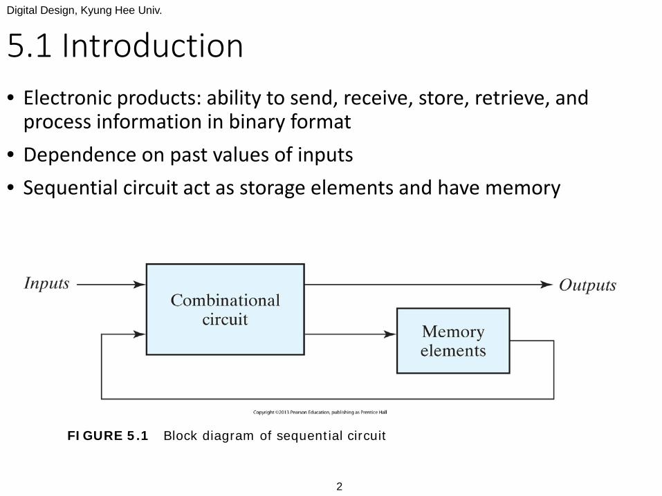
5.1 Introduction• Electronic products: ability to send, receive, store, retrieve, and
process information in binary format• Dependence on past values of inputs• Sequential circuit act as storage elements and have memory
FIGURE 5.1 Block diagram of sequential circuit
Digital Design, Kyung Hee Univ.
3
5.2 Sequential Circuits• Output: a function of inputs and the present state of the storage
elements• Next state of the storage elements: a function of external inputs
and the present state• A sequential circuit is specified by a time sequence of inputs,
outputs, and internal states• vs. Combinational circuit depends on the present values of the inputs
• Classification (timing of signals)• Asynchronous sequential circuit: at any instant of time and order
• Time-delay devices• Internal propagation delay of logic gate• Combinational circuit with feedback• Unstable at times
• Synchronous sequential circuit= clocked sequential circuit: at discrete instants of time
Digital Design, Kyung Hee Univ.
4
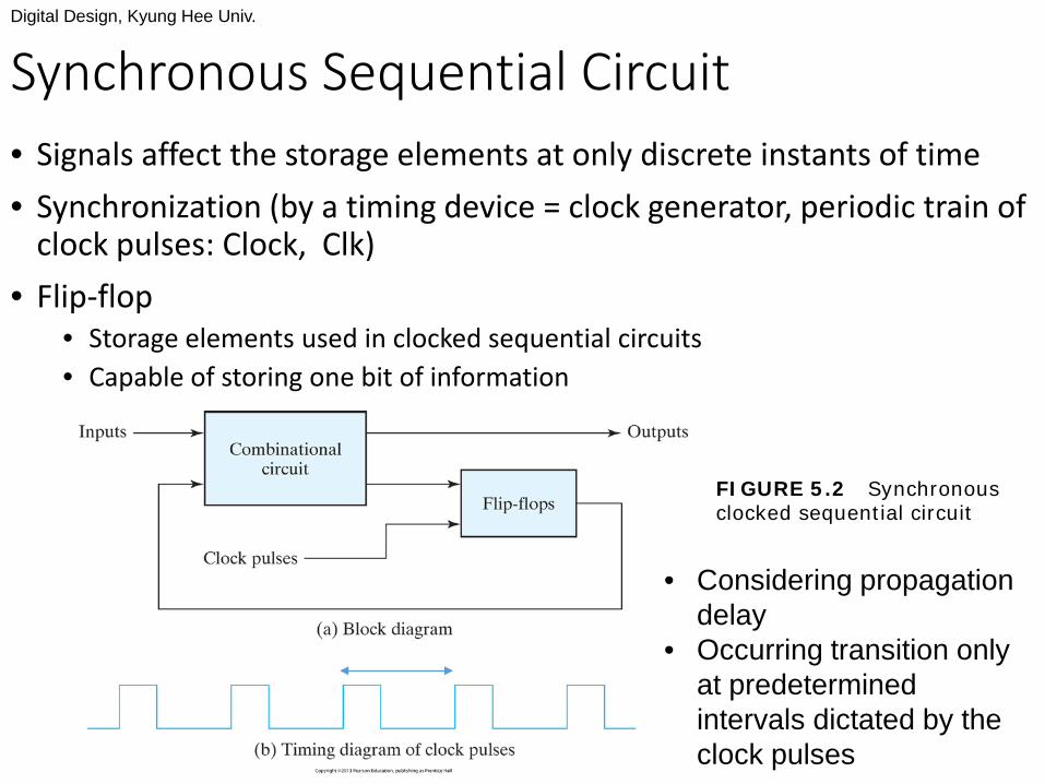
Synchronous Sequential Circuit• Signals affect the storage elements at only discrete instants of time• Synchronization (by a timing device = clock generator, periodic train of
clock pulses: Clock, Clk)• Flip-flop
• Storage elements used in clocked sequential circuits• Capable of storing one bit of information
FIGURE 5.2 Synchronous clocked sequential circuit
• Considering propagation delay
• Occurring transition only at predetermined intervals dictated by the clock pulses
Digital Design, Kyung Hee Univ.
5
5.3 Storage elements: Latches• Maintain a binary state indefinitely until directed by an input signal to
switch states• Various types of storage elements: number of inputs, manner affecting
the binary state• Level sensitive devices: Latch (operate with signal levels)
• For asynchronous sequential circuits
• Edge-sensitive devices: Flip-flops (controlled by a clock transition)• For synchronous sequential circuits
Digital Design, Kyung Hee Univ.
6
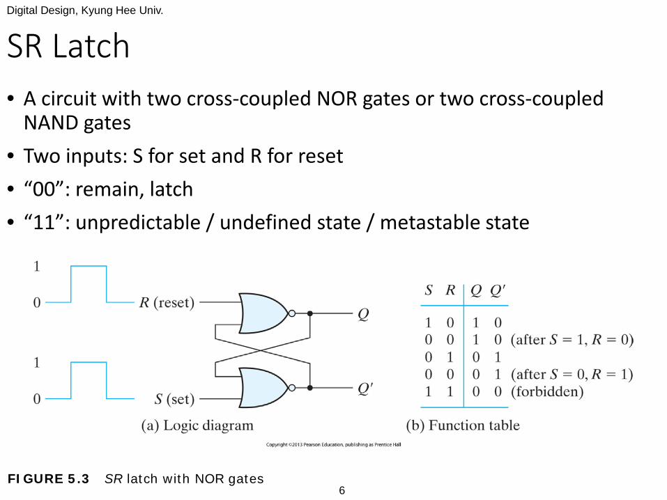
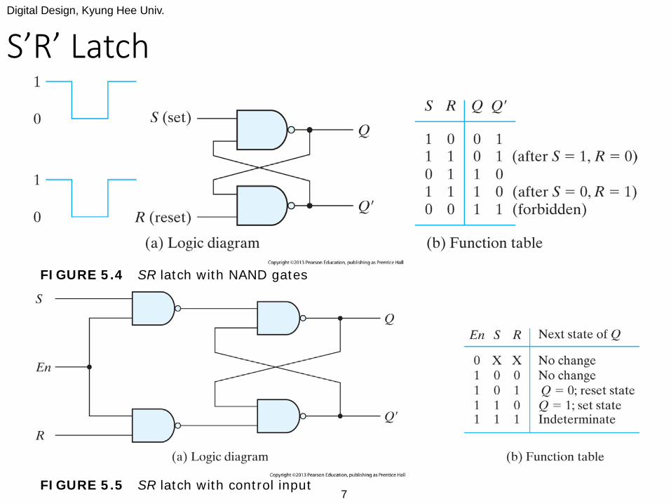
SR Latch• A circuit with two cross-coupled NOR gates or two cross-coupled
NAND gates• Two inputs: S for set and R for reset• “00”: remain, latch• “11”: unpredictable / undefined state / metastable state
FIGURE 5.3 SR latch with NOR gates
Digital Design, Kyung Hee Univ.
7
FIGURE 5.4 SR latch with NAND gates
S’R’ Latch
FIGURE 5.5 SR latch with control input
Digital Design, Kyung Hee Univ.
8
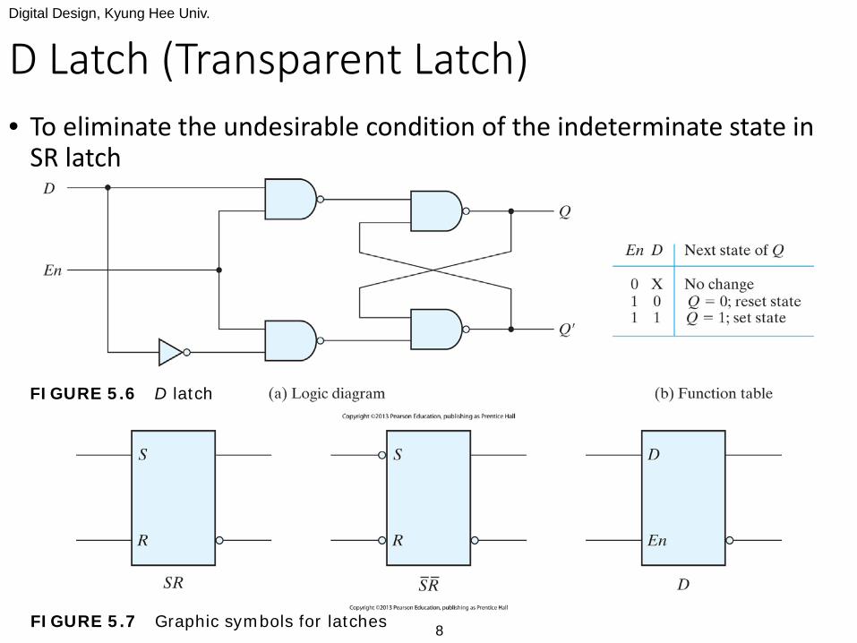
D Latch (Transparent Latch)• To eliminate the undesirable condition of the indeterminate state in
SR latch
FIGURE 5.6 D latch
FIGURE 5.7 Graphic symbols for latches
Digital Design, Kyung Hee Univ.
9
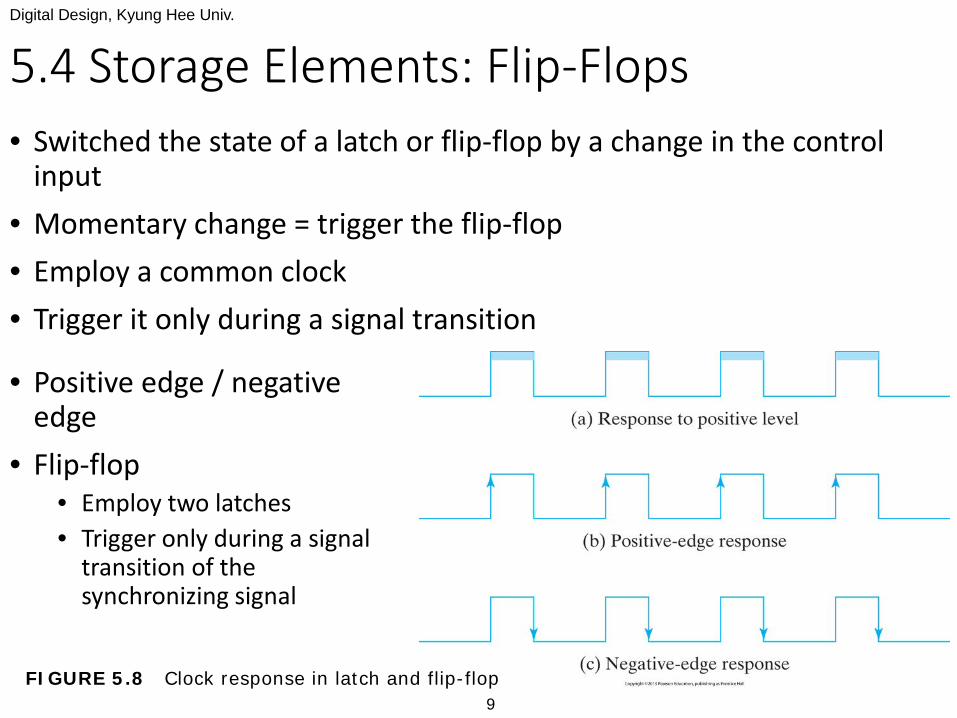
5.4 Storage Elements: Flip-Flops• Switched the state of a latch or flip-flop by a change in the control
input• Momentary change = trigger the flip-flop• Employ a common clock• Trigger it only during a signal transition
• Positive edge / negative edge
• Flip-flop• Employ two latches• Trigger only during a signal
transition of the synchronizing signal
FIGURE 5.8 Clock response in latch and flip-flop
Digital Design, Kyung Hee Univ.
10
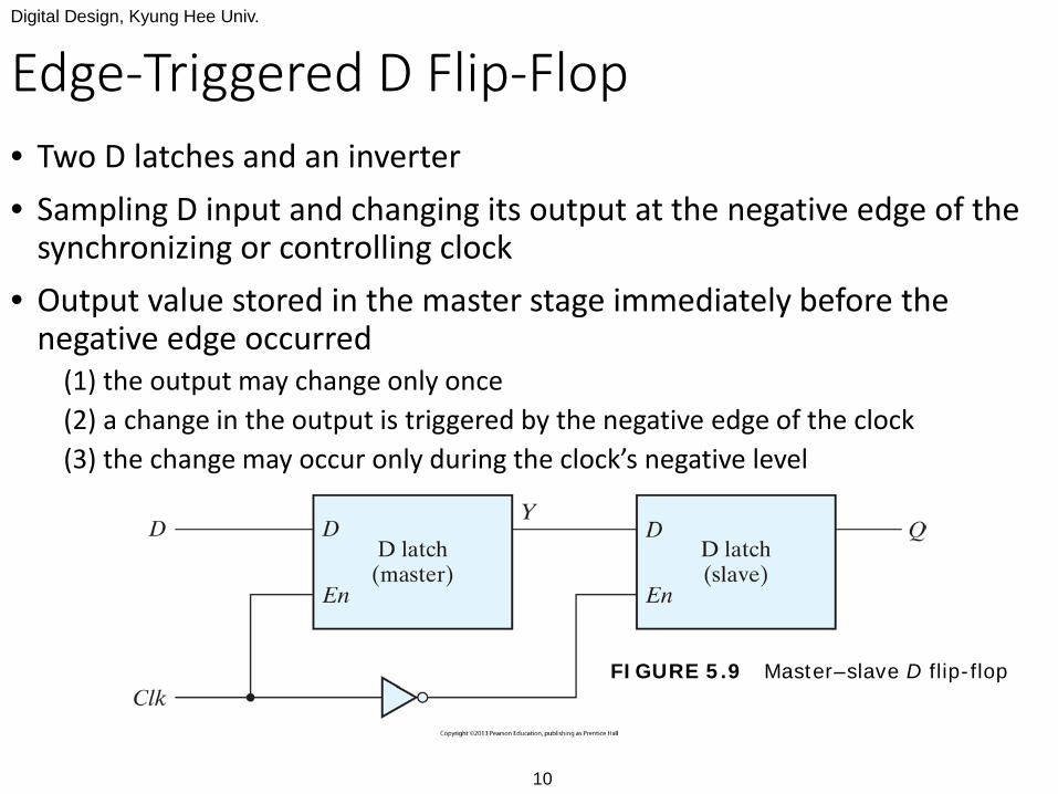
Edge-Triggered D Flip-Flop• Two D latches and an inverter• Sampling D input and changing its output at the negative edge of the
synchronizing or controlling clock• Output value stored in the master stage immediately before the
negative edge occurred(1) the output may change only once(2) a change in the output is triggered by the negative edge of the clock(3) the change may occur only during the clock’s negative level
FIGURE 5.9 Master–slave D flip-flop
Digital Design, Kyung Hee Univ.
11
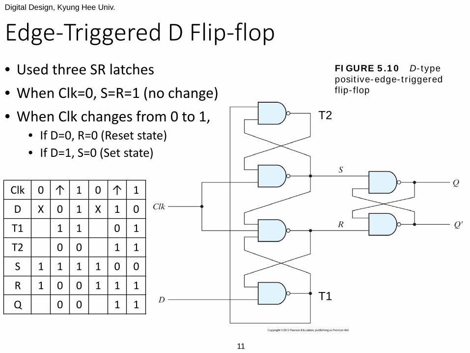
Edge-Triggered D Flip-flop• Used three SR latches• When Clk=0, S=R=1 (no change)• When Clk changes from 0 to 1,
• If D=0, R=0 (Reset state)• If D=1, S=0 (Set state)
FIGURE 5.10 D-type positive-edge-triggered flip-flop
Clk 0 ↑ 1 0 ↑ 1
D X 0 1 X 1 0
T1 1 1 0 1
T2 0 0 1 1
S 1 1 1 1 0 0
R 1 0 0 1 1 1
Q 0 0 1 1T1
T2
Digital Design, Kyung Hee Univ.
12
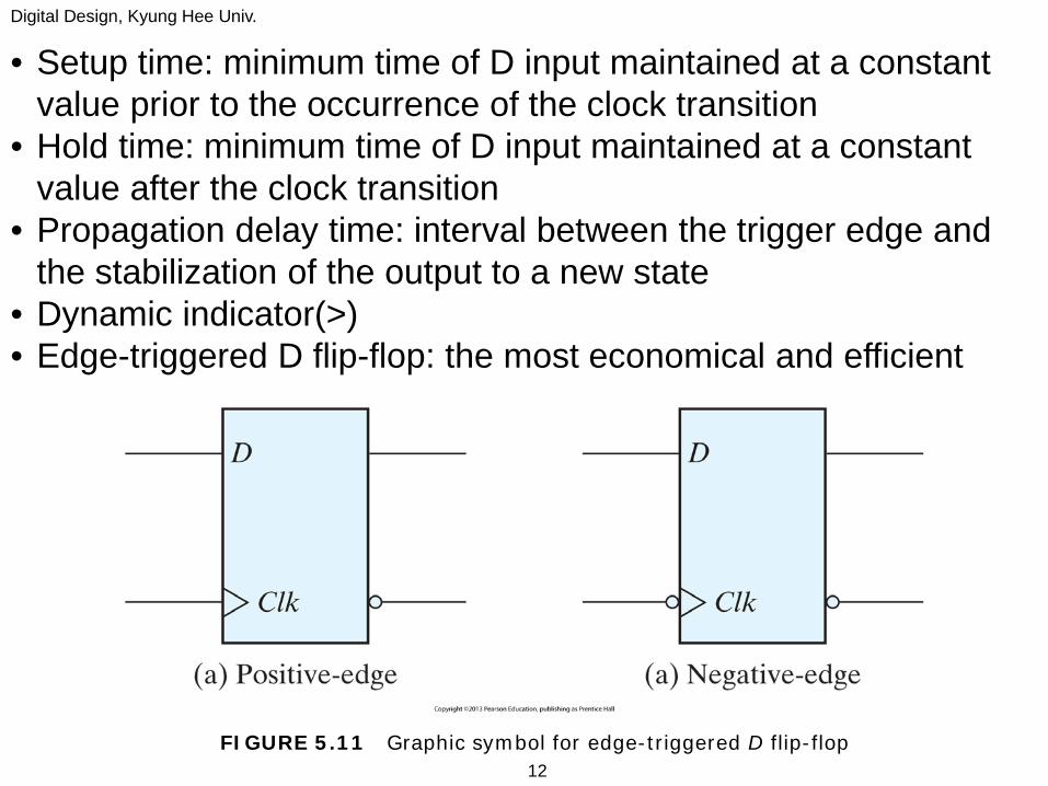
• Setup time: minimum time of D input maintained at a constant value prior to the occurrence of the clock transition
• Hold time: minimum time of D input maintained at a constant value after the clock transition
• Propagation delay time: interval between the trigger edge and the stabilization of the output to a new state
• Dynamic indicator(>)• Edge-triggered D flip-flop: the most economical and efficient
FIGURE 5.11 Graphic symbol for edge-triggered D flip-flop
Digital Design, Kyung Hee Univ.
13
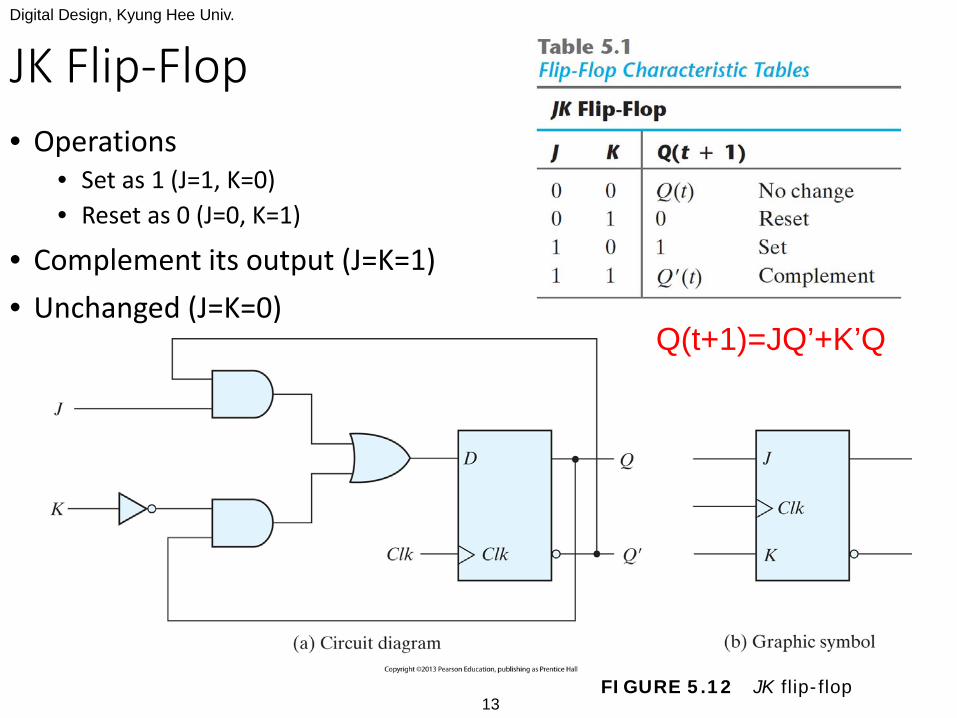
JK Flip-Flop• Operations
• Set as 1 (J=1, K=0)• Reset as 0 (J=0, K=1)
• Complement its output (J=K=1)• Unchanged (J=K=0)
FIGURE 5.12 JK flip-flop
Q(t+1)=JQ’+K’Q
Digital Design, Kyung Hee Univ.
14
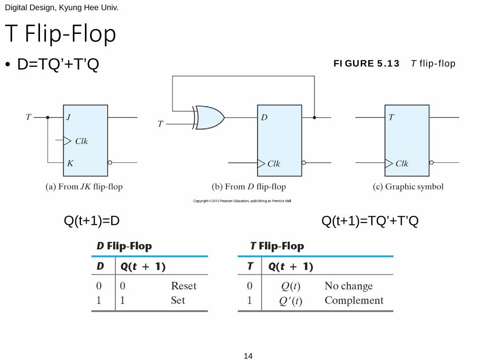
T Flip-Flop• D=TQ’+T’Q FIGURE 5.13 T flip-flop
Q(t+1)=D Q(t+1)=TQ’+T’Q
Digital Design, Kyung Hee Univ.
15
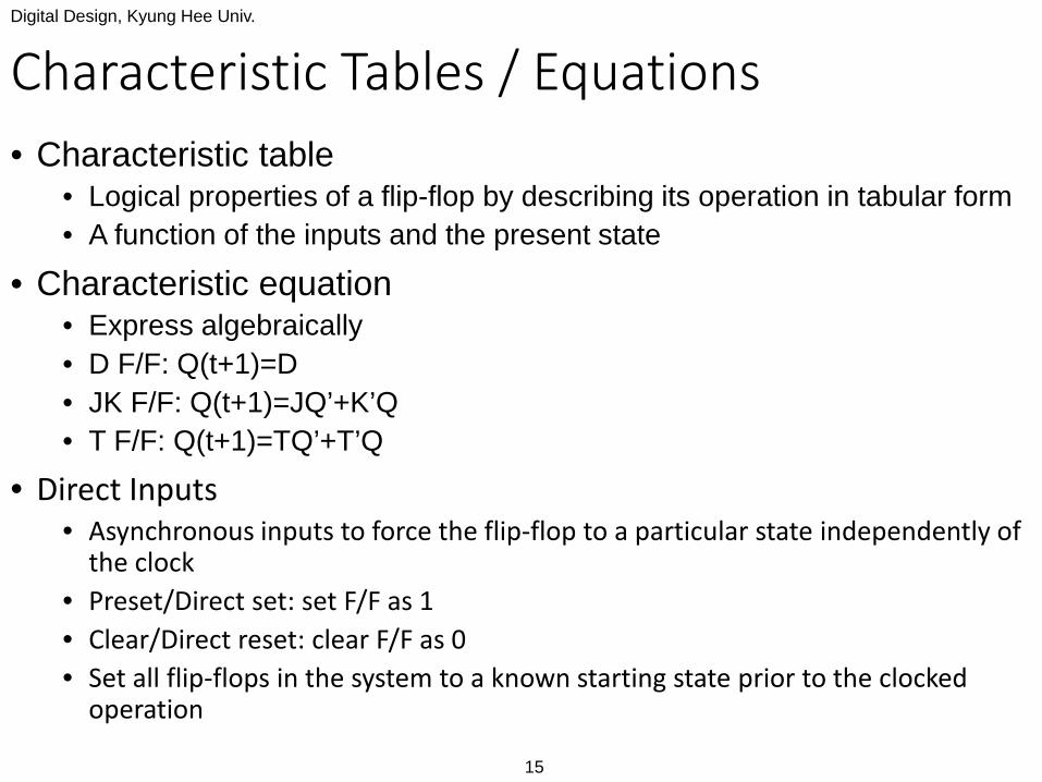
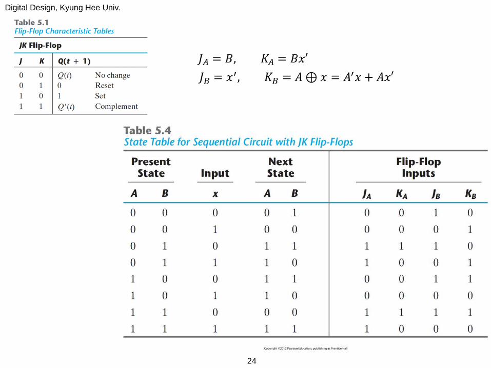
Characteristic Tables / Equations• Characteristic table
• Logical properties of a flip-flop by describing its operation in tabular form• A function of the inputs and the present state
• Characteristic equation• Express algebraically • D F/F: Q(t+1)=D• JK F/F: Q(t+1)=JQ’+K’Q• T F/F: Q(t+1)=TQ’+T’Q
• Direct Inputs• Asynchronous inputs to force the flip-flop to a particular state independently of
the clock• Preset/Direct set: set F/F as 1• Clear/Direct reset: clear F/F as 0• Set all flip-flops in the system to a known starting state prior to the clocked
operation
Digital Design, Kyung Hee Univ.
16
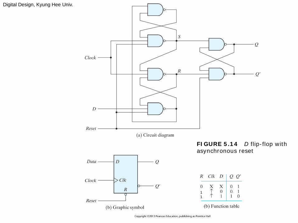
FIGURE 5.14 D flip-flop with asynchronous reset
11
Digital Design, Kyung Hee Univ.
17
5.5 Analysis of Clocked Sequential Circuits• Analysis: behavior of a given circuit under certain operating conditions• Clocked sequential circuit including flip-flops is determined from the
inputs, the outputs, and the internal state of its F/F• Representation
• Algebraic representation• State table• State diagram
• Time sequence of inputs, outputs, and internal states
Digital Design, Kyung Hee Univ.
18
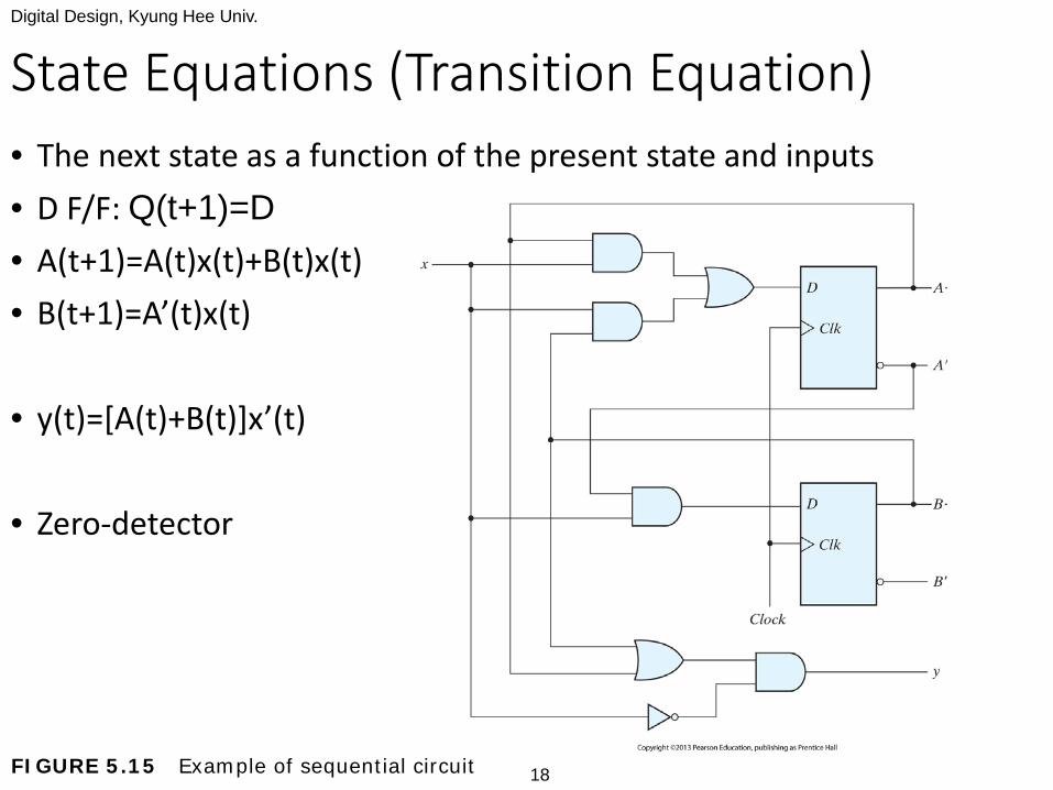
State Equations (Transition Equation)• The next state as a function of the present state and inputs• D F/F: Q(t+1)=D• A(t+1)=A(t)x(t)+B(t)x(t)• B(t+1)=A’(t)x(t)
• y(t)=[A(t)+B(t)]x’(t)
• Zero-detector
FIGURE 5.15 Example of sequential circuit
Digital Design, Kyung Hee Univ.
19
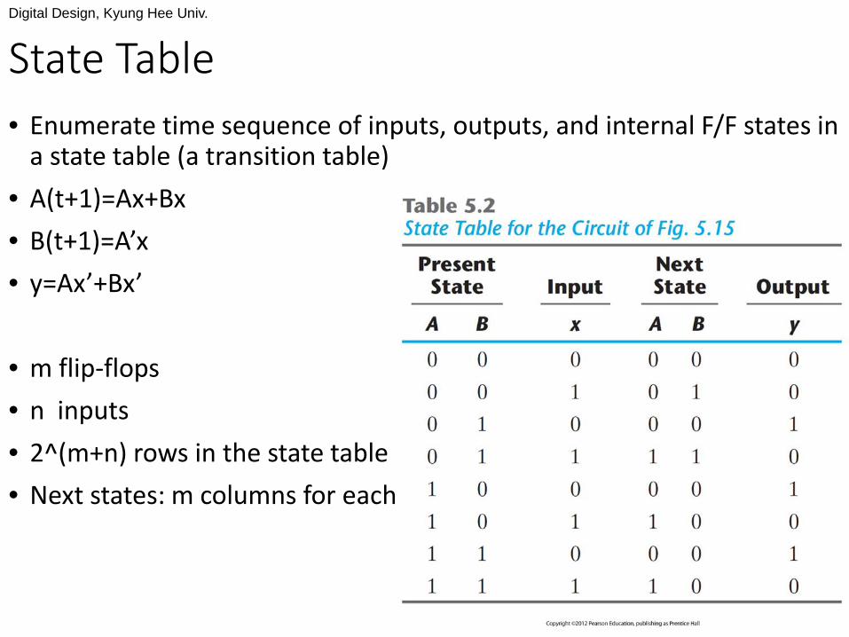
State Table• Enumerate time sequence of inputs, outputs, and internal F/F states in
a state table (a transition table)• A(t+1)=Ax+Bx• B(t+1)=A’x• y=Ax’+Bx’
• m flip-flops• n inputs• 2^(m+n) rows in the state table• Next states: m columns for each
Digital Design, Kyung Hee Univ.
20
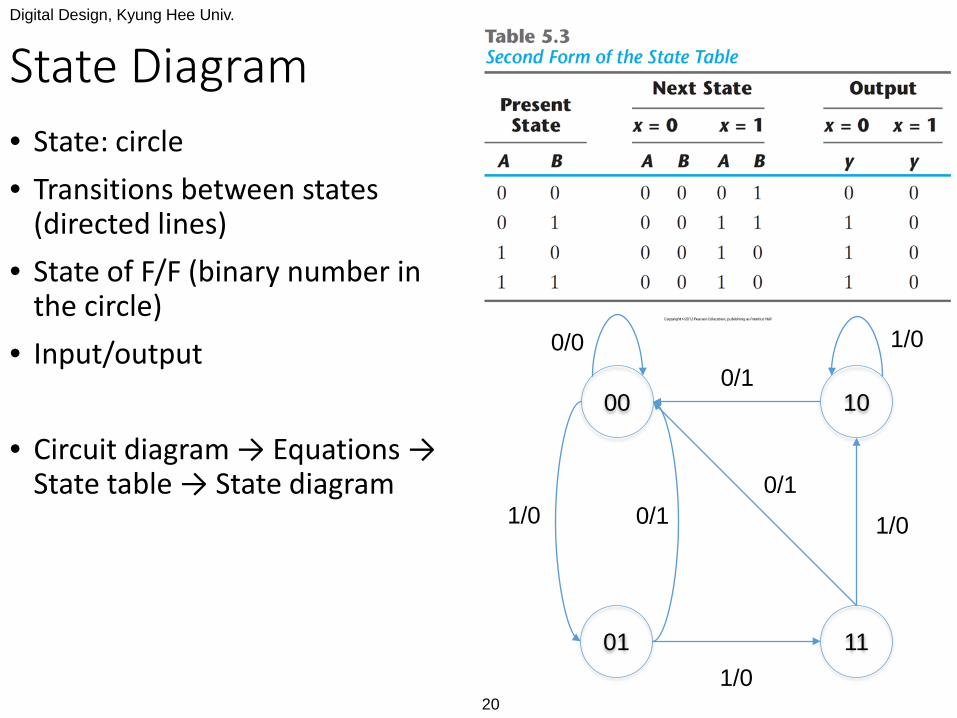
State Diagram• State: circle• Transitions between states
(directed lines)• State of F/F (binary number in
the circle)• Input/output
• Circuit diagram → Equations → State table → State diagram
00 10
01 11
0/0
1/0 0/1
1/0
0/11/0
0/11/0
Digital Design, Kyung Hee Univ.
21
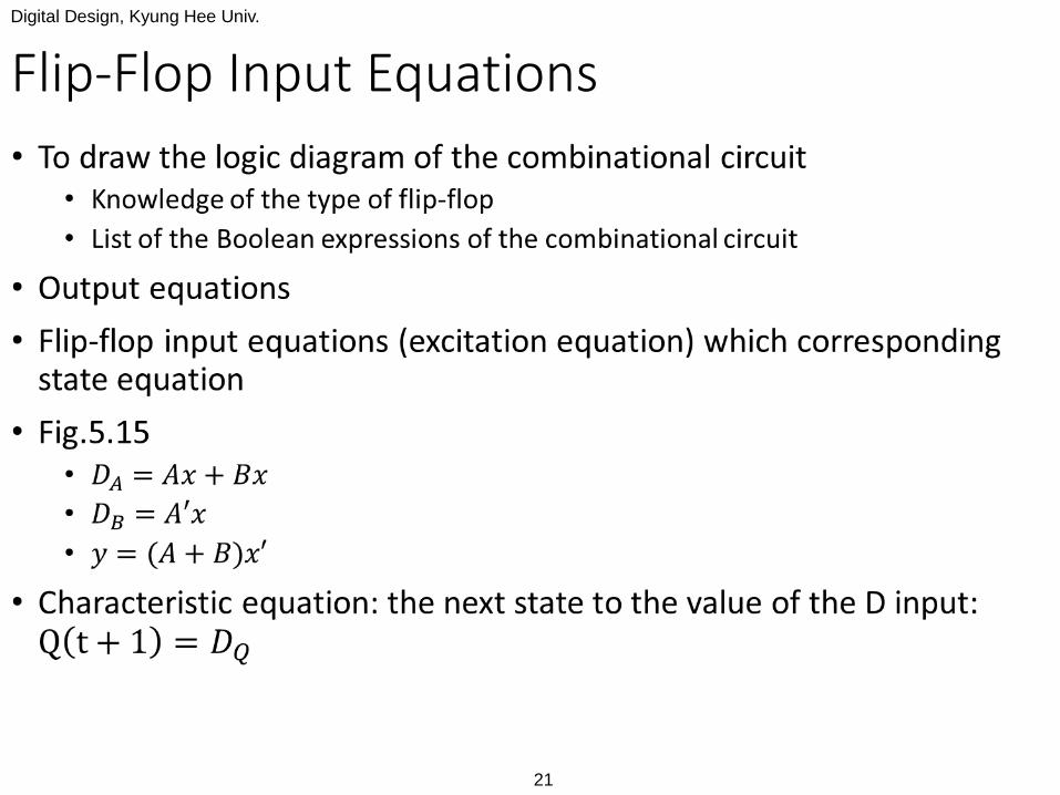
Flip-Flop Input Equations
Digital Design, Kyung Hee Univ.
22
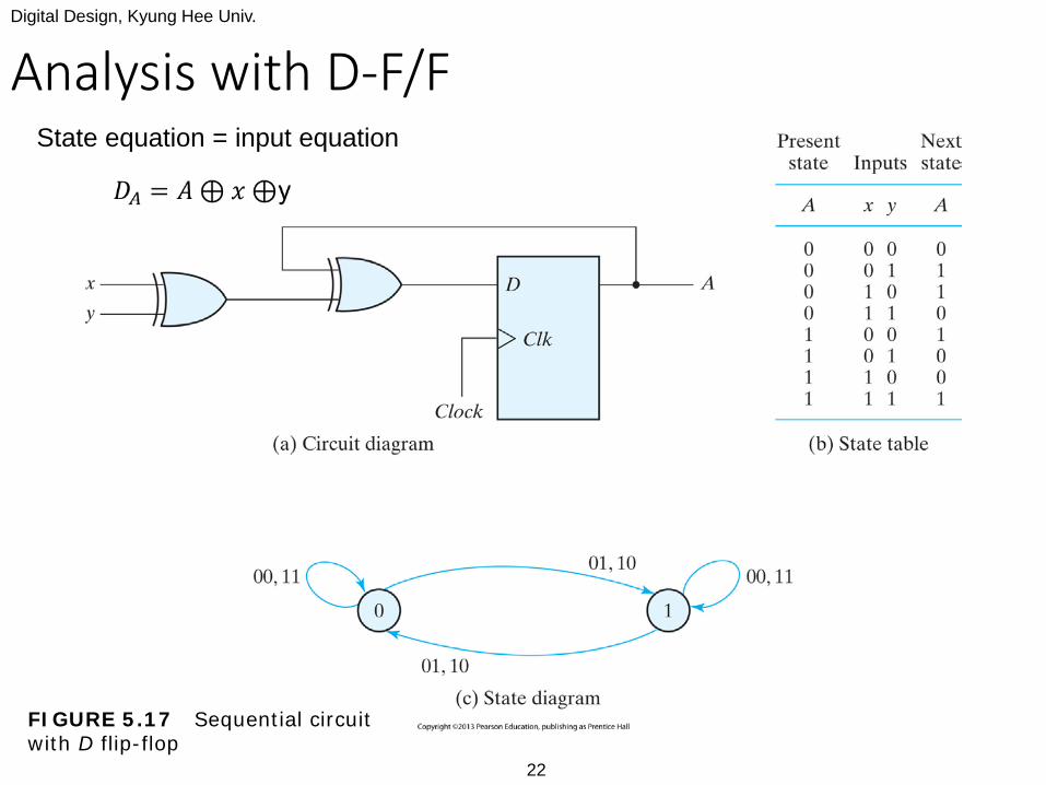
Analysis with D-F/F
FIGURE 5.17 Sequential circuit with D flip-flop
State equation = input equation
Digital Design, Kyung Hee Univ.
23
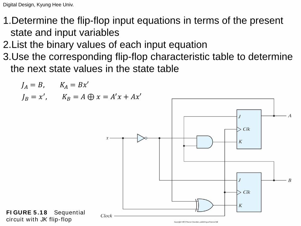
1.Determine the flip-flop input equations in terms of the present state and input variables
2.List the binary values of each input equation3.Use the corresponding flip-flop characteristic table to determine
the next state values in the state table
FIGURE 5.18 Sequential circuit with JK flip-flop
Digital Design, Kyung Hee Univ.
24
Digital Design, Kyung Hee Univ.
25
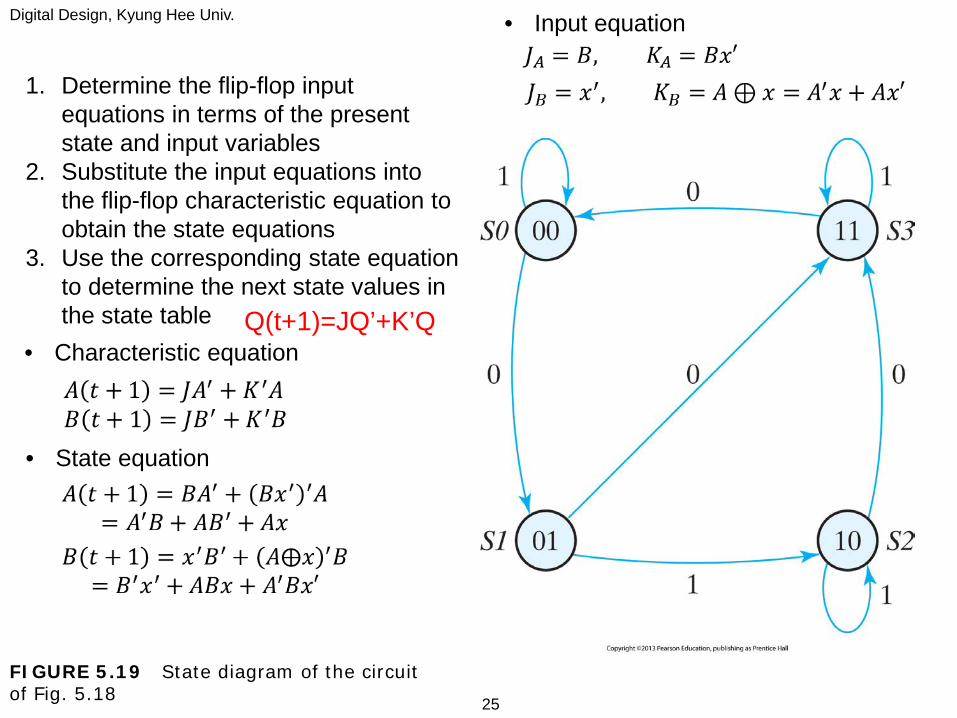
1. Determine the flip-flop input equations in terms of the present state and input variables
2. Substitute the input equations into the flip-flop characteristic equation to obtain the state equations
3. Use the corresponding state equation to determine the next state values in the state table
• State equation
• Input equation
• Characteristic equation
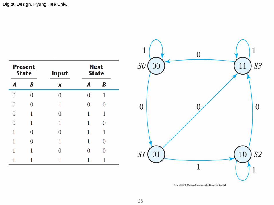
FIGURE 5.19 State diagram of the circuit of Fig. 5.18
Q(t+1)=JQ’+K’Q
Digital Design, Kyung Hee Univ.
26
Digital Design, Kyung Hee Univ.
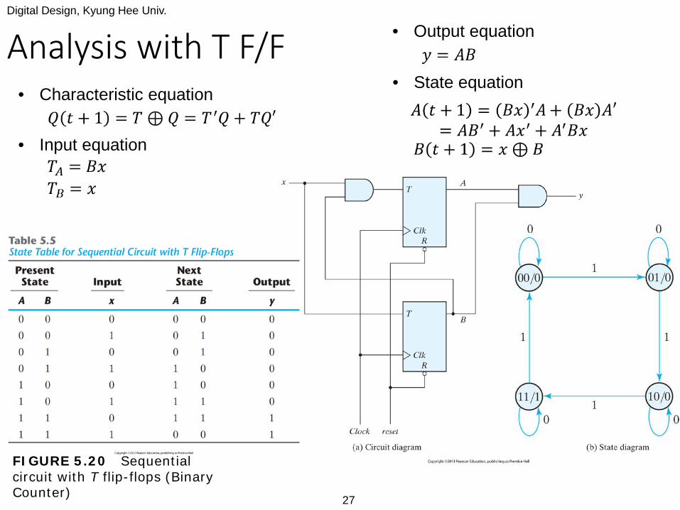
27
• Characteristic equation
• Input equation
• Output equation
• State equation
FIGURE 5.20 Sequential circuit with T flip-flops (Binary Counter)
Analysis with T F/F
Digital Design, Kyung Hee Univ.
28
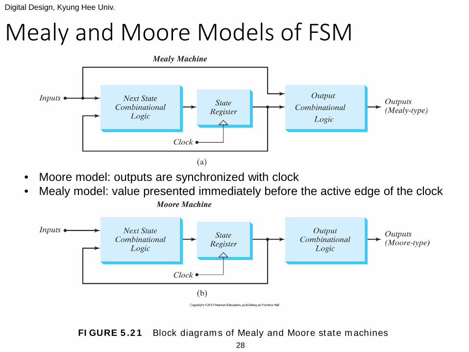
Mealy and Moore Models of FSM
FIGURE 5.21 Block diagrams of Mealy and Moore state machines
• Moore model: outputs are synchronized with clock• Mealy model: value presented immediately before the active edge of the clock
Digital Design, Kyung Hee Univ.
29
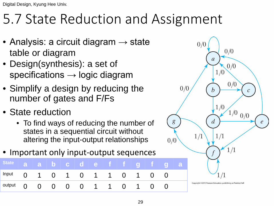
5.7 State Reduction and Assignment• Analysis: a circuit diagram → state
table or diagram• Design(synthesis): a set of
specifications → logic diagram• Simplify a design by reducing the
number of gates and F/Fs• State reduction
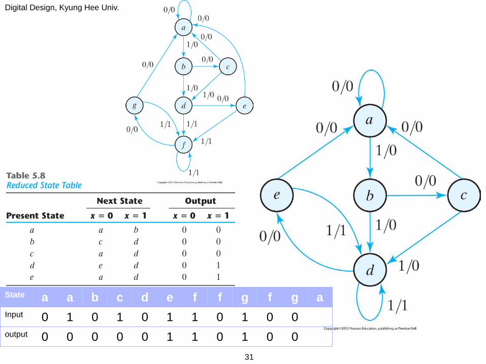
• To find ways of reducing the number of states in a sequential circuit without altering the input-output relationships
• Important only input-output sequencesState a a b c d e f f g f g aInput 0 1 0 1 0 1 1 0 1 0 0output 0 0 0 0 0 1 1 0 1 0 0
Digital Design, Kyung Hee Univ.
30
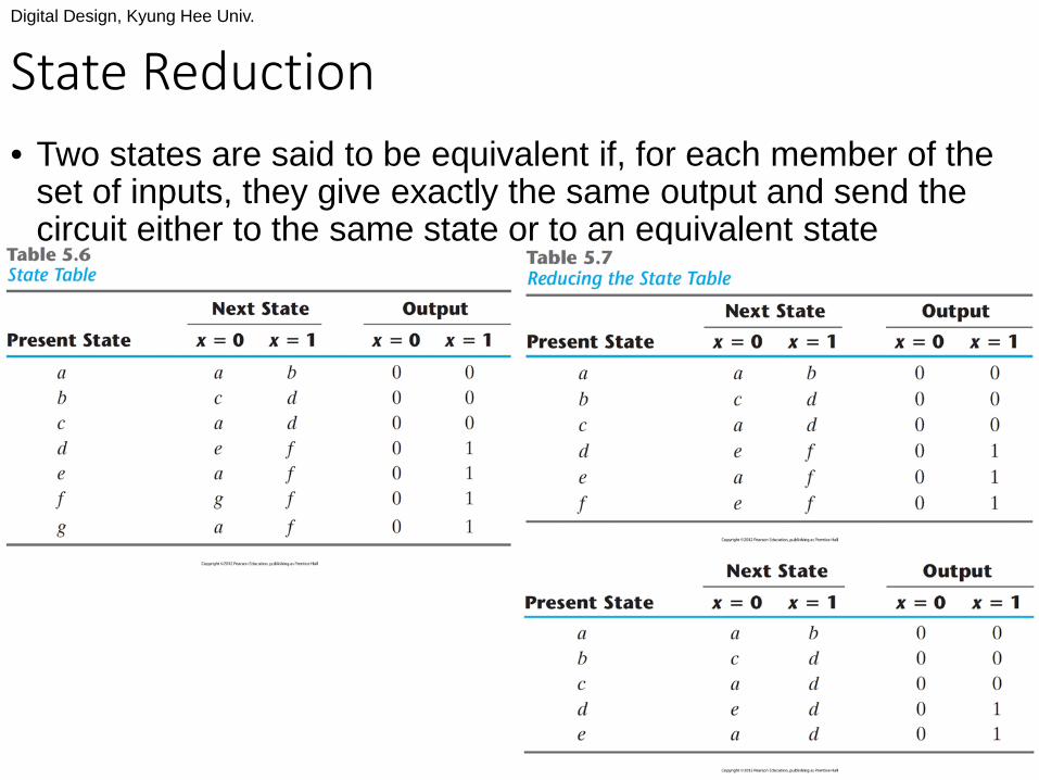
State Reduction• Two states are said to be equivalent if, for each member of the
set of inputs, they give exactly the same output and send the circuit either to the same state or to an equivalent state
Digital Design, Kyung Hee Univ.
31
State a a b c d e f f g f g aInput 0 1 0 1 0 1 1 0 1 0 0output 0 0 0 0 0 1 1 0 1 0 0
Digital Design, Kyung Hee Univ.
32
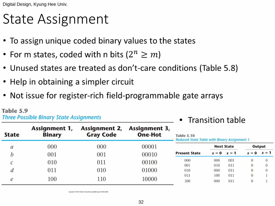
State Assignment
• Transition table
Digital Design, Kyung Hee Univ.
33
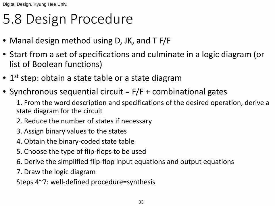
5.8 Design Procedure• Manal design method using D, JK, and T F/F• Start from a set of specifications and culminate in a logic diagram (or
list of Boolean functions)• 1st step: obtain a state table or a state diagram• Synchronous sequential circuit = F/F + combinational gates
1. From the word description and specifications of the desired operation, derive a state diagram for the circuit2. Reduce the number of states if necessary3. Assign binary values to the states4. Obtain the binary-coded state table5. Choose the type of flip-flops to be used6. Derive the simplified flip-flop input equations and output equations7. Draw the logic diagramSteps 4~7: well-defined procedure=synthesis
Digital Design, Kyung Hee Univ.
34
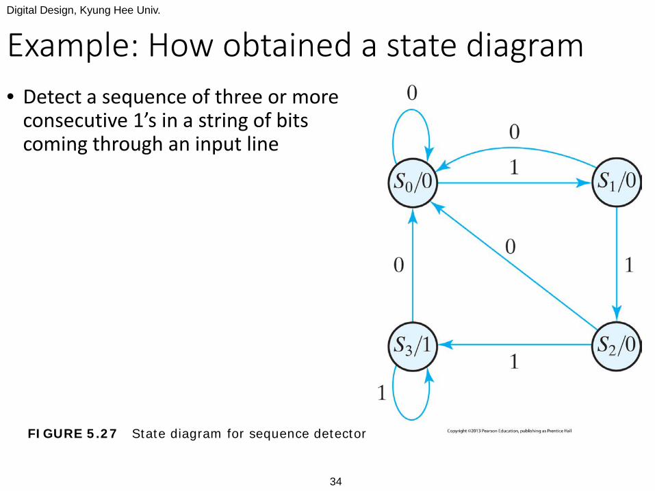
Example: How obtained a state diagram• Detect a sequence of three or more
consecutive 1’s in a string of bits coming through an input line
FIGURE 5.27 State diagram for sequence detector
Digital Design, Kyung Hee Univ.
35
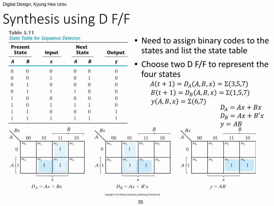
Synthesis using D F/F• Need to assign binary codes to the
states and list the state table• Choose two D F/F to represent the
four states
Digital Design, Kyung Hee Univ.
36
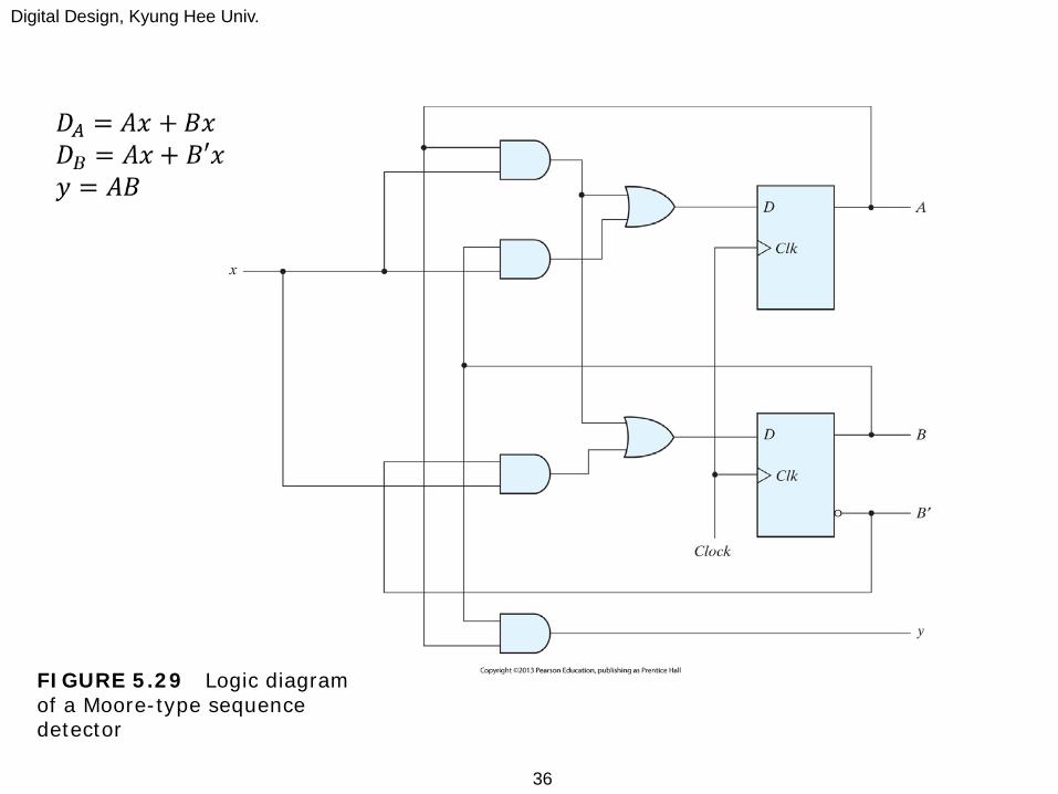
FIGURE 5.29 Logic diagram of a Moore-type sequence detector
Digital Design, Kyung Hee Univ.
37
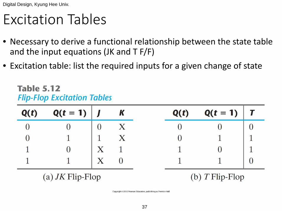
Excitation Tables• Necessary to derive a functional relationship between the state table
and the input equations (JK and T F/F)• Excitation table: list the required inputs for a given change of state
Digital Design, Kyung Hee Univ.
38
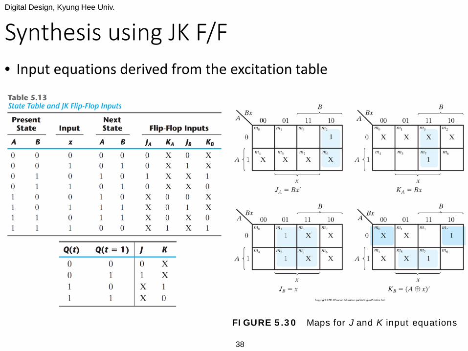
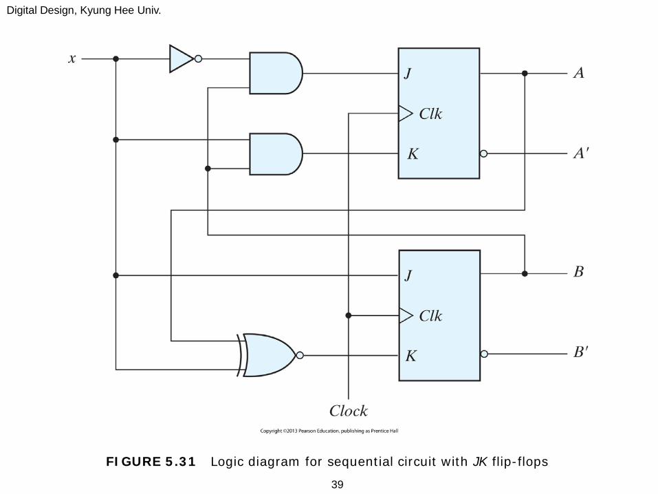
Synthesis using JK F/F• Input equations derived from the excitation table
FIGURE 5.30 Maps for J and K input equations
Digital Design, Kyung Hee Univ.
39
FIGURE 5.31 Logic diagram for sequential circuit with JK flip-flops

Digital Design, Kyung Hee Univ.
40
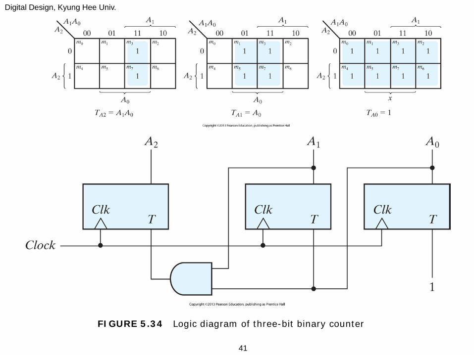
Synthesis using T F/F• Binary counter (0 to 2n-1)
Digital Design, Kyung Hee Univ.
41
FIGURE 5.34 Logic diagram of three-bit binary counter