Embed Size (px)
Citation preview

Lecture note on Physics of Semiconductors (7)26th May (2021) Shingo Katsumoto, Institute for Solid State Physics, University of Tokyo
Chapter 6 Homo·hetero junctions
So far we have seen the bulk properties of uniform semiconductors. Henceforth we go into the rich physical phe-
nomenon in spatially structures semiconductors, the actions as defices.
6.1 Electrical and optical characteristics of homo pn junctions
The pn junction is one of the first semiconductor devices for electric circuits. For the detailed history of the device, see
e.g. [1] (though in Japanese, out-of-print).
6.1.1 Thermal equilibrium
E
p NA
x
n ND-wp wn
++
++
+ +
+
+
+
+++
+
+
--- -
-- -
-- ---
--
0
DA
ee
np wNwN +
-
Ec
EvEF
eVbi
Fig. 6.1 (a) Schematic of an abrupt pn-junction. (b) Electric field E(x) in depletionlayer. x-direction is taken as positive for thefield. (c) Band diagram.
A pn junction, as it expresses, is a junction of a p-type semi-
conductor and an n-type semiconductor. Here we consider homo-
junctions, in which the same species of semiconductor is used for
p- and n-layers. In such a junction, the electron density is high in
the n-layer and the hole density in the p-layer. Hence there should
be diffusion pressures which drive electrons to the p-layer and holes
to the n-layer for increase of entropy S. On the other hand, such
diffusions charge up the p-layer to negative and the n-layer to pos-
itive creating charge double layer at the junction (charge depletionlayer). This electro-magnetically enhances the internal energy U .
In thermal equilibrium, the double layer width is determined from
the condition for free energy (U − TS) minimum.
We take a simple model of an abrupt junction (Fig. 6.1), and
p ∼ n ∼ ni in the depletion layer. We write the built-in volt-age due to the pn structure at the interface across the depletion layer
Vbi. In the process that an electron moves from the n-layer to the
p-layer, the energy increases by eVbi. In the n-layer the electron
density nn ∼ ND, and in the p-layer the semiconductor equation
tells np ∼ n2i /NA. We consider a general case that N1 and N2
electrons are respectively distributed in two boxes with site number
N . The number of cases is W = NCN1NCN2. Here only particle
exchanges are considered hence dN1 = −dN2. Under assumption N ≫ N1,2, d(lnW ) ≈ ln(N2/N1)dN1 (mixing en-tropy of gases). Applying this to the pn-junction with dN1 = −1, N1 = nn, N2 = np, condition d(U − TS)/dnn = 0
E7-1
0 10 20
100
102
104
106
108
e V k T| |/ B
|/
|J
J0
Shockley theory
Forward bias
Reverse bias
x
EFn
EFp
0
p n
eV
log ,p
logn
pp
np
nn
pn
(a) (b)
Fig. 6.2 (a) Upper panel: quasi-Fermi levels in a pn-junction under external forward voltage V . Lower panel:Spatial variation of carrier densities. (b) Broken line: I-V characteristics of Shockley theory (eq.(6.11)). Normalizedwith J0, which is the coefficient in eq.(6.11). Solid line: Realistic I-V characteristics, in which series resistance,recombination inside the depletion layer, tunneling through localized states are taken into account. The inset is alinear plot of (6.11).
gives
eVbi = kBT lnnn
np∼ kBT ln
NDNA
n2i
= Eg − kBT lnNcNv
NDNA. (6.1)
(nn ∼ ND, pp ∼ NA).
In equilibrium it is also required that the chemical potential (Fermi energy) is constant through the junction, inde-
pendent of the spatial coordinate. Far inside p, n-layers apart from the junction, the band structure should recover the
bulk states. Hence the band diagram in Fig. 6.1(c) is drawn. Let the depletion layer widths in p and n-layers wp, wn
respectively, then E(x) is given as
− ϵϵ0E(x) = NA(2x+ wp) +NDwn (x < 0), NAwp +ND(wn − 2x) (x ≥ 0), (6.2)
where ϵ is the dielectric constant. Then Vbi is calculated as
Vbi =
∫ wn
−wp
(−E(x))dx =e
ϵϵ0(ND +NA)wnwp =
e
ϵϵ0(ND +NA)
ND
NAw2
n ∵ wnND = wpNA. (6.3)
From eqs.(6.1) and (6.3), we obtain the relation between the doping concentrations and the depletion layer width.
6.1.2 Current-Voltage characteristics
In equilibrium of a pn-junction, the net current is zero as a result of balance between the entropy and the internal
energy. An externally applied voltage pushes off the balance and a current flows as a result. When the energy cost is
lowered by the voltage, the diffusion current causes injection of minority carriers. Minority carrier injection is an action
that increases density of minority carrier dynamically. The minority carrier injection breaks the semiconductor equation
np = n2i locally. Even in such circumstances, by introducing quasi-Fermi level, we can treat electrons and holes as in
quasi-equilibriums and apply the Boltzmann equation to obtain carrier fluxes. The semiconductor equation (law of mass
E7-2
action) can also be recovered in a bit modified manner. The goal here is to give the net current as a function of external
voltage.
We model the effect of external voltage V as follows. All the voltage drops outside the depletion layer are ignored and
V is applied inside it. Far from the junction, the current is carried by majority carriers, which have high concentration
and the gradient in the chemical potential in such regions is ignorable. Around the depletion layer, imbalance between the
internal energy cost and the increase of entropy causes a flow of carriers. V is applied against Vbi lowering the barrier for
diffusion currents, then the majority carriers flows into the counter layers increasing the minority carrier densities at the
depletion layer edges. The injected minority carriers diffuse into the bulk, recombine with majority carriers and disappear.
The diffusion-annihilation process forms a exponential decay in the steady minority carrier density distribution.
In the above model, we assume that local thermal equilibrium is attained in each thin layer parallel to yz plane through
the carrier-carrier interaction and the particles can be exchanged between neighboring layers. Quasi-Fermi levels, which
depends on x-coordinate, for electrons (µe(x)) and holes (µh(x)) are introduced as follows,
n(x) = Nc exp[−(Ec(x)− µe(x))/kBT ], p(x) = Nv exp[−(µh(x)− Ev(x))/kBT ], (6.4a)
i.e., µe(x) = Ec(x) + kBT lnn(x)
Nc, µh(x) = Ev(x)− kBT ln
p(x)
Nv. (6.4b)
The diffusion of minority carriers (densities np, pn) is described by the following diffusion equations.
Ded2np
dx2=
np − np0
τe−G(x), Dh
d2pndx2
=pn − pn0
τh−G(x), (6.5)
where G(x) represents minority carrier creation e.g. by light illumination and in the dark G(x) = 0. np0, pn0 are
minority carrier concentrations in the bulk regions, De,h, τe,h are the diffusion constant and the lifetime respectively (e
for electrons, h for holes). Then minority carrier diffusion lengths for electrons and holes are
Le =√Deτe, Lh =
√Dhτh. (6.6)
The solution for (6.5) (pn for x > wn, np for x < −wp) which satisfies the boundary condition np → np0 (x → −∞)
and pn → pn0 (x → ∞), is obtained as
np(x) = δn0 exp
(x+ wp
Le
)+ np0, pn(x) = δp0 exp
(−x− wn
Lh
)+ pn0, (6.7)
where δn0, δp0 are concentrations of injected minority carriers at the edges of the depletion layer. From the definition
(6.4b), in the region of diffusion and with ignoring np0, pn0 in (6.7), the quasi-Fermi levels linearly depend on the
distances as
µe(x) = Ec + kBT
[x+ wp
Le+ ln
δn0
Nc
], µh(x) = Ev − kBT
[x− wn
Lh+ ln
δp0Nv
]. (6.8)
These should join the bulk values E(p),(n)F at x → ±∞ respectively and E
(p),(n)F differ by eV , i.e., E(p)
F − E(n)F = eV .
Therefore they are schematically drawn as in Fig. 6.2(a).
We ignore electron-hale recombination inside the depletion layer and assume the currents are limited by the diffusion
of minority carriers. Then the net current density is the sum of minority carrier diffusion currents at the two edges of the
depletion layer. From eq.(6.7) and eq.Fig. 6.2(a),
δn0 + np0 = n(−wp) = np0 expeV
kBT, δp0 + pn0 = p(wn) = pn0 exp
eV
kBT. (6.9)
The electron diffusion current density at x = −wp in the process (6.5) is thus
je = eDednp
dx
∣∣∣∣−wp
=eDeδn0
Le=
eDe
Lenp0
[exp
eV
kBT− 1
]. (6.10)
E7-3

x
pp
np
nn
pn
Gte
Gth
pn0
np0
ln, ln
pn
J
V
Jsc
Voc
(a) (b)
Fig. 6.3 (a) Carrier density distribution around a pn-junction under photo-generation of minority carriers G. De-pletion layer edges are indicated by perpendicular broken lines. Bias is taken as shortage V = 0. (b) Schematic I-Vcharacteristics in the dark and under illumination.
The hole current can be calculated in the same way and the net current is given as
j = e
[De
Lenp0 +
Dh
Lhpn0
] [exp
eV
kBT− 1
]≈ en2
i
[De
LeNA+
Dh
LhND
] [exp
eV
kBT− 1
]. (6.11)
Equation (6.11) is the very basics of the Schottky theory of pn-junction. Though the model grabs the essence, real pn
junctions are much more complicated. Important modifications are series resistance, recombination in depletion layer and
tunneling conductance through localized level inside energy gap (parallel Ohmic resistance). With these modifications, a
realistic characteristics shown in Fig. 6.2(b) differs considerably from the Shockley theory.
6.1.3 Photo-response of pn-junctions
Let us take the simplest model for a pn-junction under illumination assuming majority carrier generation G(x) does
not depend on x (a constant G) in the diffusion equation (6.5). Just as before, the solution for np(x) and pn(x) which
satisfies the boundary condition np → nn0 +Gτe for x → −∞, and pn → pn0 +Gτh for x → ∞ is
np(x) = np0 +Gτe +
[np0
(exp
(eV
kBT
)− 1
)−Gτe
]exp
(x+ wp
Le
), (6.12a)
pn(x) = pn0 +Gτh +
[pn0
(exp
(eV
kBT
)− 1
)−Gτh
]exp
(−x− wn
Lh
). (6.12b)
The solution for V = 0 is schematically drawn in Fig. 6.3(a).
From the solution, the net current density is given as
j = j0
[exp
eV
kBT− 1
]− eG(Le + Lh), (6.13)
where j0 is the coefficient in front of the parentheses in (6.11). Equation (6.13) is a simple negative shift of (6.11) by
jsc ≡ G(τe + τh). Figure 6.3(b) shows the characteristics. Real solar cells are more complicated but the common is
the negative shift of the current characteristics with illumination. The parameters which characterize each device are the
negative shift at short-circuit condition |JSC| (short circuit current) and the voltage at open-circuit condition VOC (opencircuit voltage). These depend, of course, on the strength and the spectrum of illumination.
In the characteristics shown in Fig. 6.3(b), the cell pumps out an electric energy under the bias condition in the fourth
quadrant. Current J and voltage V give power W = |JV |. In the forth quadrant |J | ≤ |JSC|, |V | ≤ |VOC| then
W ≤ |JSCVOC|. Then Jmax, Vmax which give the maximum power is determined and
FF ≡ JmaxVmax
JSCVOC≤ 1 (6.14)
E7-4
is called filling factor (FF). The better the squareness of the I-V characteristics, the higher the FF. JSC, VOC, and FF are
useful parameters for discussing phenomenology of solar cells, modeling equivalent circuits. In the ideal characteristics
(6.13),
|JSC| = eG(Le + Lh), VOC =kBT
eln
[eG(τe + τh)
j0+ 1
]. (6.15)
The above is the basics of photoelectric conversion and applied to e.g. solar cells. For the solar cells see the article by
the present author [2] (in Japanese).
6.2 pn-junction transistors
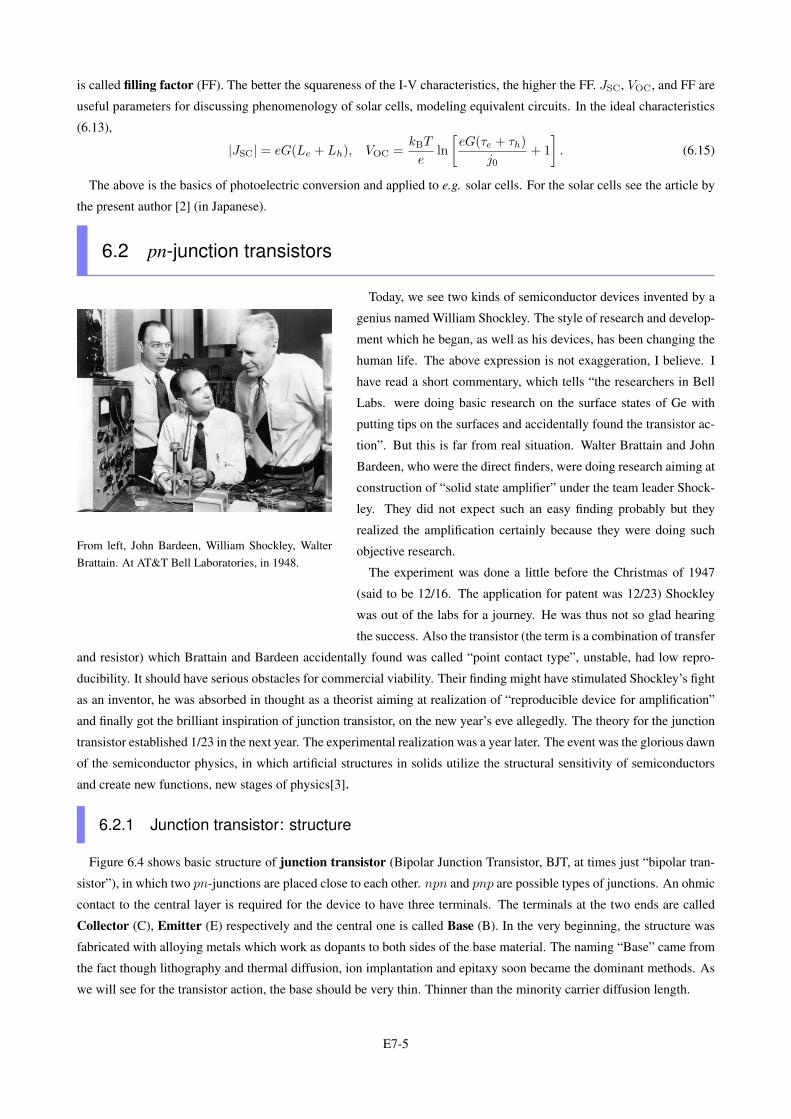
From left, John Bardeen, William Shockley, WalterBrattain. At AT&T Bell Laboratories, in 1948.
Today, we see two kinds of semiconductor devices invented by a
genius named William Shockley. The style of research and develop-
ment which he began, as well as his devices, has been changing the
human life. The above expression is not exaggeration, I believe. I
have read a short commentary, which tells “the researchers in Bell
Labs. were doing basic research on the surface states of Ge with
putting tips on the surfaces and accidentally found the transistor ac-
tion”. But this is far from real situation. Walter Brattain and John
Bardeen, who were the direct finders, were doing research aiming at
construction of “solid state amplifier” under the team leader Shock-
ley. They did not expect such an easy finding probably but they
realized the amplification certainly because they were doing such
objective research.
The experiment was done a little before the Christmas of 1947
(said to be 12/16. The application for patent was 12/23) Shockley
was out of the labs for a journey. He was thus not so glad hearing
the success. Also the transistor (the term is a combination of transfer
and resistor) which Brattain and Bardeen accidentally found was called “point contact type”, unstable, had low repro-
ducibility. It should have serious obstacles for commercial viability. Their finding might have stimulated Shockley’s fight
as an inventor, he was absorbed in thought as a theorist aiming at realization of “reproducible device for amplification”
and finally got the brilliant inspiration of junction transistor, on the new year’s eve allegedly. The theory for the junction
transistor established 1/23 in the next year. The experimental realization was a year later. The event was the glorious dawn
of the semiconductor physics, in which artificial structures in solids utilize the structural sensitivity of semiconductors
and create new functions, new stages of physics[3].
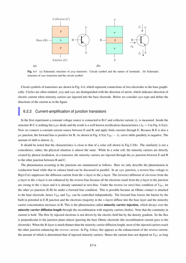
6.2.1 Junction transistor: structure
Figure 6.4 shows basic structure of junction transistor (Bipolar Junction Transistor, BJT, at times just “bipolar tran-
sistor”), in which two pn-junctions are placed close to each other. npn and pnp are possible types of junctions. An ohmic
contact to the central layer is required for the device to have three terminals. The terminals at the two ends are called
Collector (C), Emitter (E) respectively and the central one is called Base (B). In the very beginning, the structure was
fabricated with alloying metals which work as dopants to both sides of the base material. The naming “Base” came from
the fact though lithography and thermal diffusion, ion implantation and epitaxy soon became the dominant methods. As
we will see for the transistor action, the base should be very thin. Thinner than the minority carrier diffusion length.
E7-5
B B
C C
E E
p
p
p
n
n
n
C
E
B
JB
JC
JE
Collector (C)
Emitter (E)
Base (B)
(a) (b)
Fig. 6.4 (a) Schematic structure of pnp transistor. Circuit symbol and the names of terminals. (b) Schematicstructure of npn transistor and the circuit symbol.
Circuit symbols of transistors are shown in Fig. 6.4, which represent connections of two electrodes to the base graphi-
cally. Circles are often omitted. pnp and npn are distinguished with the direction of arrow, which indicates direction of
electric current when minority carriers are injected into the base electrode. Below we consider npn-type and define the
directions of the current as in the figure.
6.2.2 Current-amplification of junction transistors
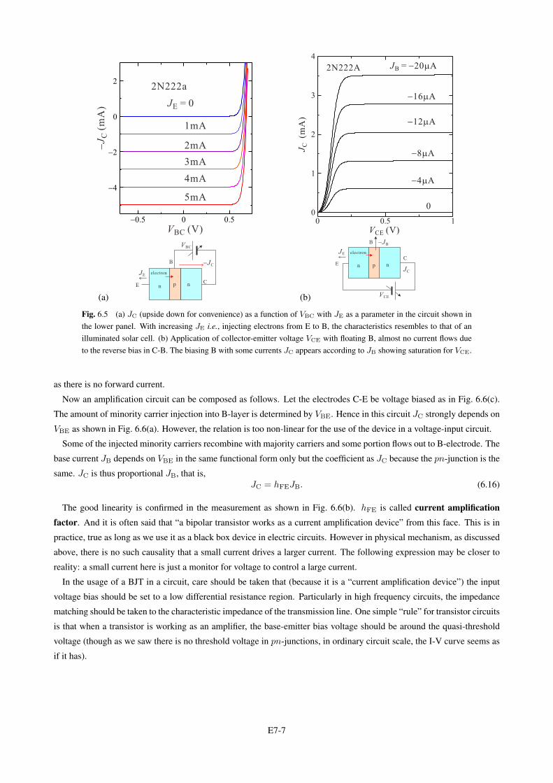
In the first experiment a constant voltage source is connected to B-C and collector current JC is measured. Inside the
structure B-C is nothing but a pn diode and the result is a well known rectification characteristics (JE = 0 in Fig. 6.5(a)).
Now we connect a constant current source between E and B, and apply finite currents through E. Because B-E is also a
pn junction, the forward bias is positive for B. As shown in Fig. 6.5(a) VBC − JC curve shifts parallely to negative. The
amount of shift is almost JE.
It should be noted that the characteristics is close to that of a solar cell shown in Fig.2.3(b). The similarity is not a
coincidence, rather, the physical situation is almost the same. While In a solar cell, the minority carriers are directly
created by photon irradiation, in a transistor, the minority carriers are injected through the pn junction between E and B
to the other junction between B and C.
The phenomenon occurring in the junctions are summarised as follows. Here we only describe the phenomenon in
conduction band while that in valence band can be discussed in parallel. In an npn junction, a reverse bias voltage to
B(p)-C(n) suppresses the diffusion current from the n-layer to the p-layer. The (reverse) diffusion of electrons from the
p-layer to the n-layer is not enhanced by the reverse bias because all the electrons reach from the p-layer to the junction
are swung to the n-layer and it is already saturated at zero-bias. Under the reverse (or zero) bias condition of VBC, let
the other pn-junction (E-B) be under a forward bias condition. This is possible because an Ohmic contact is attached
to the base electrode, hence VEB and VBC can be controlled independently. The forward bias lowers the barrier by the
built-in potential in E-B junction and the electrons (majority in the n-layer) diffuse into the base layer and the minority
carrier concentration increases in B. This is the phenomenon called minority carrier injection, which decays over the
minority carrier diffusion length through the recombination with majority carriers (holes). Note that the continuity in
current is hold. The flow by injected electrons is not driven by the electric field but by the density gradient. So the flux
is perpendicular to the junction plane almost ignoring the base Ohmic electrode (the recombination current goes to the
electrode). When the B-layer is much thinner than the minority carrier diffusion length, most of the injected carriers reach
the other junction enhancing the reverse current. In Fig. 6.6(a), this appears as the enhancement of the reverse current,
the amount of which is determined that of injected minority carriers. Hence the current does not depend on VBC as long
E7-6
-0.5 0 0.5
-4
-2
0
2
VBC (V)
2N222a
-J
C(m
A) JE = 0
1mA
2mA
3mA
4mA
5mA
0 0.5 10
1
2
3
4
2N222A
VCE (V)
JC
( mA
)
JB = 20 A- m
-16mA
-12mA
-8mA
-4mA
0
(a)
p nnC
E
B
VBC
-JC
JE electron
(b)
p nn
CE
B
VCE
JC
-JB
JE electron
Fig. 6.5 (a) JC (upside down for convenience) as a function of VBC with JE as a parameter in the circuit shown inthe lower panel. With increasing JE i.e., injecting electrons from E to B, the characteristics resembles to that of anilluminated solar cell. (b) Application of collector-emitter voltage VCE with floating B, almost no current flows dueto the reverse bias in C-B. The biasing B with some currents JC appears according to JB showing saturation for VCE.
as there is no forward current.
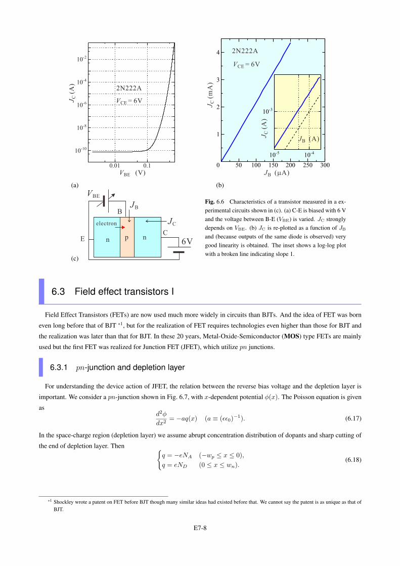
Now an amplification circuit can be composed as follows. Let the electrodes C-E be voltage biased as in Fig. 6.6(c).
The amount of minority carrier injection into B-layer is determined by VBE. Hence in this circuit JC strongly depends on
VBE as shown in Fig. 6.6(a). However, the relation is too non-linear for the use of the device in a voltage-input circuit.
Some of the injected minority carriers recombine with majority carriers and some portion flows out to B-electrode. The
base current JB depends on VBE in the same functional form only but the coefficient as JC because the pn-junction is the
same. JC is thus proportional JB, that is,JC = hFEJB. (6.16)
The good linearity is confirmed in the measurement as shown in Fig. 6.6(b). hFE is called current amplificationfactor. And it is often said that “a bipolar transistor works as a current amplification device” from this face. This is in
practice, true as long as we use it as a black box device in electric circuits. However in physical mechanism, as discussed
above, there is no such causality that a small current drives a larger current. The following expression may be closer to
reality: a small current here is just a monitor for voltage to control a large current.
In the usage of a BJT in a circuit, care should be taken that (because it is a “current amplification device”) the input
voltage bias should be set to a low differential resistance region. Particularly in high frequency circuits, the impedance
matching should be taken to the characteristic impedance of the transmission line. One simple “rule” for transistor circuits
is that when a transistor is working as an amplifier, the base-emitter bias voltage should be around the quasi-threshold
voltage (though as we saw there is no threshold voltage in pn-junctions, in ordinary circuit scale, the I-V curve seems as
if it has).
E7-7
0.01 0.1
10-10
10-8
10-6
10-4
10-2
2N222A
VCE = 6V
VBE (V)
JC
(A)
0 50 100 150 200 250 300
1
2
3
4
10-5 10-4
10-3
2N222A
VCE = 6V
JC
( A)
JC
(mA
)
JB ( A)m
JB (A)
(a) (b)
(c)
p nnC
E
B
VBE
JC
JB
6V
electron
Fig. 6.6 Characteristics of a transistor measured in a ex-perimental circuits shown in (c). (a) C-E is biased with 6 Vand the voltage between B-E (VBE) is varied. JC stronglydepends on VBE. (b) JC is re-plotted as a function of JB
and (because outputs of the same diode is observed) verygood linearity is obtained. The inset shows a log-log plotwith a broken line indicating slope 1.
6.3 Field effect transistors I
Field Effect Transistors (FETs) are now used much more widely in circuits than BJTs. And the idea of FET was born
even long before that of BJT *1, but for the realization of FET requires technologies even higher than those for BJT and
the realization was later than that for BJT. In these 20 years, Metal-Oxide-Semiconductor (MOS) type FETs are mainly
used but the first FET was realized for Junction FET (JFET), which utilize pn junctions.
6.3.1 pn-junction and depletion layer
For understanding the device action of JFET, the relation between the reverse bias voltage and the depletion layer is
important. We consider a pn-junction shown in Fig. 6.7, with x-dependent potential ϕ(x). The Poisson equation is given
asd2ϕ
dx2= −aq(x) (a ≡ (ϵϵ0)
−1). (6.17)
In the space-charge region (depletion layer) we assume abrupt concentration distribution of dopants and sharp cutting of
the end of depletion layer. Then {q = −eNA (−wp ≤ x ≤ 0),
q = eND (0 ≤ x ≤ wn).(6.18)
*1 Shockley wrote a patent on FET before BJT though many similar ideas had existed before that. We cannot say the patent is as unique as that ofBJT.
E7-8
p n
e V V( + )bi
-
-
-
-
-
-
+
+
+
+
+
+
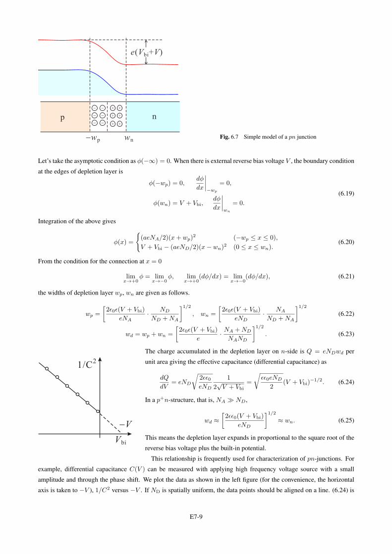
wn-wpFig. 6.7 Simple model of a pn junction
Let’s take the asymptotic condition as ϕ(−∞) = 0. When there is external reverse bias voltage V , the boundary condition
at the edges of depletion layer is
ϕ(−wp) = 0,dϕ
dx
∣∣∣∣−wp
= 0,
ϕ(wn) = V + Vbi,dϕ
dx
∣∣∣∣wn
= 0.
(6.19)
Integration of the above gives
ϕ(x) =
{(aeNA/2)(x+ wp)
2 (−wp ≤ x ≤ 0),
V + Vbi − (aeND/2)(x− wn)2 (0 ≤ x ≤ wn).
(6.20)
From the condition for the connection at x = 0
limx→+0
ϕ = limx→−0
ϕ, limx→+0
(dϕ/dx) = limx→−0
(dϕ/dx), (6.21)
the widths of depletion layer wp, wn are given as follows.
wp =
[2ϵ0ϵ(V + Vbi)
eNA· ND
ND +NA
]1/2, wn =
[2ϵ0ϵ(V + Vbi)
eND· NA
ND +NA
]1/2(6.22)
wd = wp + wn =
[2ϵ0ϵ(V + Vbi)
e· NA +ND
NAND
]1/2. (6.23)
-V
1/C2
Vbi
The charge accumulated in the depletion layer on n-side is Q = eNDwd per
unit area giving the effective capacitance (differential capacitance) as
dQ
dV= eND
√2ϵϵ0eND
1
2√V + Vbi
=
√ϵϵ0eND
2(V + Vbi)
−1/2. (6.24)
In a p+n-structure, that is, NA ≫ ND,
wd ≈[2ϵϵ0(V + Vbi)
eND
]1/2≈ wn. (6.25)
This means the depletion layer expands in proportional to the square root of the
reverse bias voltage plus the built-in potential.
This relationship is frequently used for characterization of pn-junctions. For
example, differential capacitance C(V ) can be measured with applying high frequency voltage source with a small
amplitude and through the phase shift. We plot the data as shown in the left figure (for the convenience, the horizontal
axis is taken to −V ), 1/C2 versus −V . If ND is spatially uniform, the data points should be aligned on a line. (6.24) is
E7-9
valid only for V > 0 and C → ∞ cannot be realized. But with extrapolation from V > 0 the point 1/C2 = 0 can be
specified and we obtain Vbi from this.
When ND is not uniform spatially or some deep level traps exist, we obtain information of the spatial distribution from
differentiating the plot. Application of pulses in V and analysis of transient response under light illumination or related
techniques can bring much of the information inside the semiconductor[4].
6.3.2 Junction Field Effect Transistors
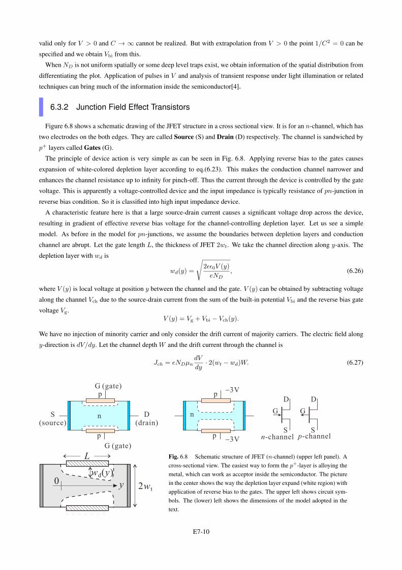
Figure 6.8 shows a schematic drawing of the JFET structure in a cross sectional view. It is for an n-channel, which has
two electrodes on the both edges. They are called Source (S) and Drain (D) respectively. The channel is sandwiched by
p+ layers called Gates (G).
The principle of device action is very simple as can be seen in Fig. 6.8. Applying reverse bias to the gates causes
expansion of white-colored depletion layer according to eq.(6.23). This makes the conduction channel narrower and
enhances the channel resistance up to infinity for pinch-off. Thus the current through the device is controlled by the gate
voltage. This is apparently a voltage-controlled device and the input impedance is typically resistance of pn-junction in
reverse bias condition. So it is classified into high input impedance device.
A characteristic feature here is that a large source-drain current causes a significant voltage drop across the device,
resulting in gradient of effective reverse bias voltage for the channel-controlling depletion layer. Let us see a simple
model. As before in the model for pn-junctions, we assume the boundaries between depletion layers and conduction
channel are abrupt. Let the gate length L, the thickness of JFET 2wt. We take the channel direction along y-axis. The
depletion layer with wd is
wd(y) =
√2ϵϵ0V (y)
eND, (6.26)
where V (y) is local voltage at position y between the channel and the gate. V (y) can be obtained by subtracting voltage
along the channel Vch due to the source-drain current from the sum of the built-in potential Vbi and the reverse bias gate
voltage Vg.V (y) = Vg + Vbi − Vch(y).
We have no injection of minority carrier and only consider the drift current of majority carriers. The electric field along
y-direction is dV/dy. Let the channel depth W and the drift current through the channel is
Jch = eNDµndV
dy· 2(wt − wd)W. (6.27)
n n
p p
p p
D D
S S
G G
-3V
-3V
G (gate)
G (gate)
S(source)
D(drain)
n-channel p-channel
y 2wt
wd( )y
L
0
Fig. 6.8 Schematic structure of JFET (n-channel) (upper left panel). Across-sectional view. The easiest way to form the p+-layer is alloying themetal, which can work as acceptor inside the semiconductor. The picturein the center shows the way the depletion layer expand (white region) withapplication of reverse bias to the gates. The upper left shows circuit sym-bols. The (lower) left shows the dimensions of the model adopted in thetext.
E7-10

In steady state there is no charging up and Jch is uniform through the channel thus integration over the channel should
be JchL.
JchL =
∫ L
0
Jchdy = 2eNDµnW
∫ L
0
(wt − wd)dV
dydy = 2wteNDµnW
∫ VL
V0
(1− wd
wt
)dV. (6.28)
Let the critical voltage Vc at which the channel is pinched (wd = wt) and Jch = 0 then Vc = eNDw2t /2ϵϵ0. Hence from
wd/wt =√
V/Vc, Jch in this model is obtained as
Jch =2NDeµnWwt
L
[VL − V0 +
2
3√Vc
(V (V0)3/2 − V (VL)
3/2)
]. (6.29)
In eq.(6.29), at small voltages, the first linear term in VL is dominant and Jch increases linearly. With increasing the
voltage, the last V 3/2L term grows and at last the current begins decreasing, which means negative differential resistance.
In actual device, this does not occur and Jch simply saturates with increasing V . The model contains various shortages,
e.g., the equipotential lines are straight and along x-axis. Improved models can reproduce the saturation but they are
inevitably complicated. There are also empirical analytical formulas well fit to the experiments but they have no physical
reasoning.
Appendix 6A: Analysis of pn junction transistor
Let us have a brief look at the simplest analysis of charrier statistics in bipolar transistors.
6A.1 Current-voltage characteristics
Figure 6A.1 illustrates the bias conditions and the carrier concentrations in an npn-type transistor. We take the x-axis
along the device current direction, and the depletion layer edge at the emitter side of the base is set to x = 0. The electron
(minority carrier) concentration at x = 0 is
np(0) = np0 expeVBE
kBT. (6A.1)
They diffuse the base region and reach the depletion edge at the other side x = WB. From there the electrons are
immediately swept out to the collector by the electric field in the depletion layer. Hence the electron concentration in the
vicinity of WB should be very small.
np(WB) = np0 exp−eVBC
kBT≈ 0. (6A.2)
Providing that WB is much shorter than the minority carrier diffusion length, we can ignore the carrier recombination and
the diffusion current in the base is constant. Equation (5.12) tells the current is proportional to dnp/dx. Hence np varies
n0E n0C
p0E p0C
p xp( )
n xp( )
xdepletion 0depletion
emitter
emitter
base
base
collector
collector
pn n
VBE VBC(a) (b) WB
linear ,n plog ,n p log ,n p
Fig. 6A.1 (a) Biasing condition of the npn transistor under consideration. (b) Schematic diagram of carrier concen-trations in a npn type transistor. In the base the ordinate is in linear scale while logarithmic in other regions.
E7-11
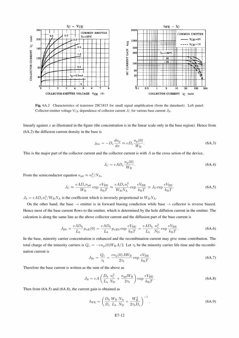
Fig. 6A.2 Characteristics of transistor 2SC1815 for small signal amplification (from the datasheet). Left panel:Collector-emitter voltage VCE dependence of collector current JC for various base current JB.
linearly against x as illustrated in the figure (the concentration is in the linear scale only in the base region). Hence from
(6A.2) the diffusion current density in the base is
jDe = −Dednp
dx≈ eDe
np(0)
WB. (6A.3)
This is the major part of the collector current and the collector current is with A as the cross setion of the device,
JC = eADenp(0)
WB. (6A.4)
From the semiconductor equation np0 ≈ n2i /NA,
JC ≈ eADenp0
WBexp
eVBE
kBT≈ eADen
2i
WBNAexp
eVBE
kBT≡ JS exp
eVBE
kBT. (6A.5)
JS = eADen2i /WBNA is the coefficient which is inversely proportional to WBNA.
On the other hand, the base → emitter is in forward biasing condiction while base → collector is reverse biased.
Hence most of the base current flows to the emitter, which is determined by the hole diffution current in the emitter. The
calcution is along the same line as the above collector current and the diffusion part of the base current is
JBh =eADh
LhpnE(0) =
eADh
LhpnE0 exp
eVBE
kBT=
eADh
Lh
n2i
NDexp
eVBE
kBT. (6A.6)
In the base, minority carrier concentration is enhanced and the recombination current may give some contribution. The
total charge of the minority carriers is Qe = −enp(0)WBA/2. Let τb be the minority carrier life time and the recombi-
nation current is
JBr =Qe
τb=
enp(0)AWB
2τbexp
eVBE
kBT. (6A.7)
Therefore the base current is written as the sum of the above as
JB = eA
(Dh
Lh
n2i
ND+
np0WB
2τb
)exp
eVBE
kBT. (6A.8)
Then from (6A.5) and (6A.8), the current gain is obtained as
hFE =
(Dh
De
WB
Lh
NA
ND+
W 2B
2τbDe
)−1
. (6A.9)
E7-12
6A.2 Effect of depletion layer width
Figure 6A.2 shows the characteristics of a transistor numbered 2SC1815 (Toshiba, Co. Ltd.). The right panel shows
hFE as a function of JC. hFE is almost constant in the low JC region indicating good linearity. On the other hand, the left
panel shows JC as a functionof VCE with JB as a parameter. In this panel, in the region VCE ≈ 0, the base-collector is
forward biased and not in the region of current amplification. Even in the current amplificatio region, JC increases with
VCE. This is called the Early effect caused by the widening of the depletion layer thus by the thinning of the base width
WB.
Let ∆W be the variation in the width of base width and the collector current is given as
JC = eADenp(0)
WB −∆W≈ eADe
np(0)
WB
(1 +
∆W
W
)≡ JC0
(1 +
∆W
W
). (6A.10)
∆W grows rapidly with VCE as in (6.23) when VCE is small while the rate lowers with VCE. In Fig. 6A.2, such tendency
is apparent. In Fig. 6.5(b), the Early effect is small and the increase in JC can be approximated to be linear in VCE.
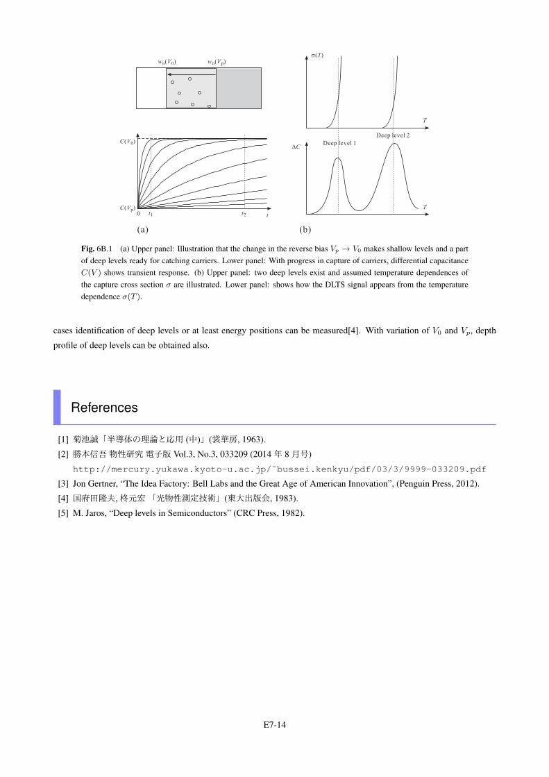
付録 6B:Deep level transient spectroscopy (DLTS)
Here I would like to give qualitative explanation on the basic principles of Deep Level Transient Spectroscopy (DLTS).
For details, see e.g. ref. [4]. We consider modification to effective capacitance (6.24), which depends on the reverse bias
voltage V . Let ND be the shallow donor concentration, NP the one for a deep donor. In the region where this deep donor
responds to change in the bias voltage, the voltage-differential capacitance is expressed as a function of reverse voltage
V as
wd(V ) ≈[2ϵϵ0(V + Vbi)
e(ND +NP)
]1/2≈ wn, (6B.1)
C(V ) =
√ϵϵ0e(ND +NP)
2(V + Vbi)
−1/2. (6B.2)
For simplicity, we consider the situation that the reverse bias Vp is applied and kept for sufficiently long time for electrons
to escape from the depletion layer including the deep levels *2. Now V is abruptly lowered to V0 < Vp and the carriers are
captured by the donor levels within w(V0) < x ≤ w(Vp). Shallow donors have high capture rate and can respond within
ms without delay, deep levels, on the other hand, the capture rate strongly depends on temperature and with decreasing
temperature, the average time for capture often elongates from ms to s, min, hour and sometimes day. Then if we open up
a fixed time window and observe the time evolution of C, the time dependence is observed in the time window at some
temperature range and in low or high temperature regions the effect of deep levels does not observed.
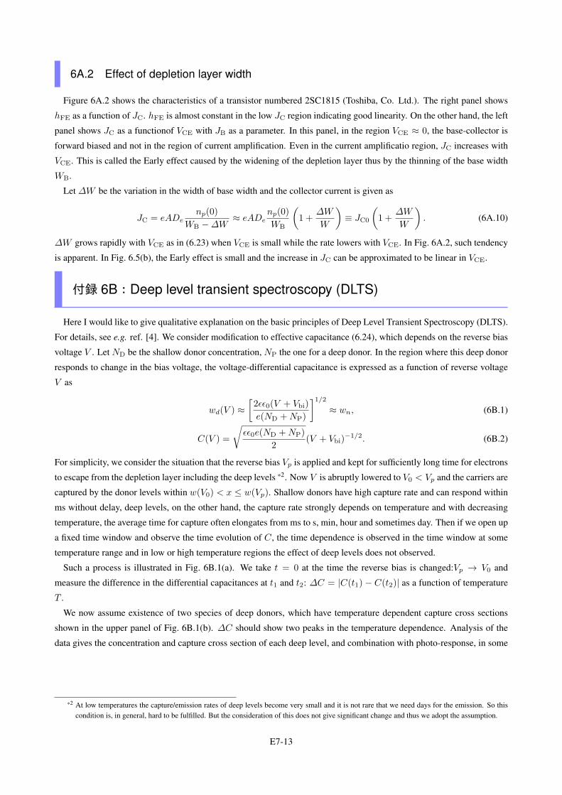
Such a process is illustrated in Fig. 6B.1(a). We take t = 0 at the time the reverse bias is changed:Vp → V0 and
measure the difference in the differential capacitances at t1 and t2: ∆C = |C(t1)− C(t2)| as a function of temperature
T .
We now assume existence of two species of deep donors, which have temperature dependent capture cross sections
shown in the upper panel of Fig. 6B.1(b). ∆C should show two peaks in the temperature dependence. Analysis of the
data gives the concentration and capture cross section of each deep level, and combination with photo-response, in some
*2 At low temperatures the capture/emission rates of deep levels become very small and it is not rare that we need days for the emission. So thiscondition is, in general, hard to be fulfilled. But the consideration of this does not give significant change and thus we adopt the assumption.
E7-13
t0C V( )p
C V( )0
t1 t2
T
T
s( )T
Deep level 1
Deep level 2
DC
w Vn 0( ) w Vn p( )
(a) (b)
Fig. 6B.1 (a) Upper panel: Illustration that the change in the reverse bias Vp → V0 makes shallow levels and a partof deep levels ready for catching carriers. Lower panel: With progress in capture of carriers, differential capacitanceC(V ) shows transient response. (b) Upper panel: two deep levels exist and assumed temperature dependences ofthe capture cross section σ are illustrated. Lower panel: shows how the DLTS signal appears from the temperaturedependence σ(T ).
cases identification of deep levels or at least energy positions can be measured[4]. With variation of V0 and Vp, depth
profile of deep levels can be obtained also.
References
[1] 菊池誠「半導体の理論と応用 (中)」(裳華房, 1963).
[2] 勝本信吾物性研究電子版 Vol.3, No.3, 033209 (2014年 8月号)
http://mercury.yukawa.kyoto-u.ac.jp/˜bussei.kenkyu/pdf/03/3/9999-033209.pdf
[3] Jon Gertner, “The Idea Factory: Bell Labs and the Great Age of American Innovation”, (Penguin Press, 2012).
[4] 国府田隆夫,柊元宏「光物性測定技術」(東大出版会, 1983).
[5] M. Jaros, “Deep levels in Semiconductors” (CRC Press, 1982).
E7-14