Embed Size (px)
Citation preview

Chapter 6
Flip-Flops and Simple Flip-Flop Applications

J. C. Huang, 2004 Digital Logic Design 1
Basic bistable element
• It is a circuit having two stable conditions (states).
• It can be used to store binary symbols.
J. C. Huang, 2004 Digital Logic Design 2
Flip-flops
A flip-flop is a bistable device, with inputs, that remains in a given state as long as power is applied and until input signals are applied to cause its output to change.

J. C. Huang, 2004 Digital Logic Design 3
Latches vs. flip-flops
• Latches are flip-flops for which the timing of the output changes are not controlled.
• For a latch, the output essentially responds immediately to changes on the input lines (and possibly the presence of a clock pulse).
• A flip-flop is designed to change its output at the edge of a controlling clock signal.

J. C. Huang, 2004 Digital Logic Design 4
SR (Set-Reset) latch
J. C. Huang, 2004 Digital Logic Design 5
Next state
• If Q denotes the present state of a memory device, i.e., the state at the time the input signals are applied, we shall use Q+ or Q(t+1) to denote the next state, i.e., the new state assumed by the device in response to the input signals.

J. C. Huang, 2004 Digital Logic Design 6
R’S’ latch
J. C. Huang, 2004 Digital Logic Design 7
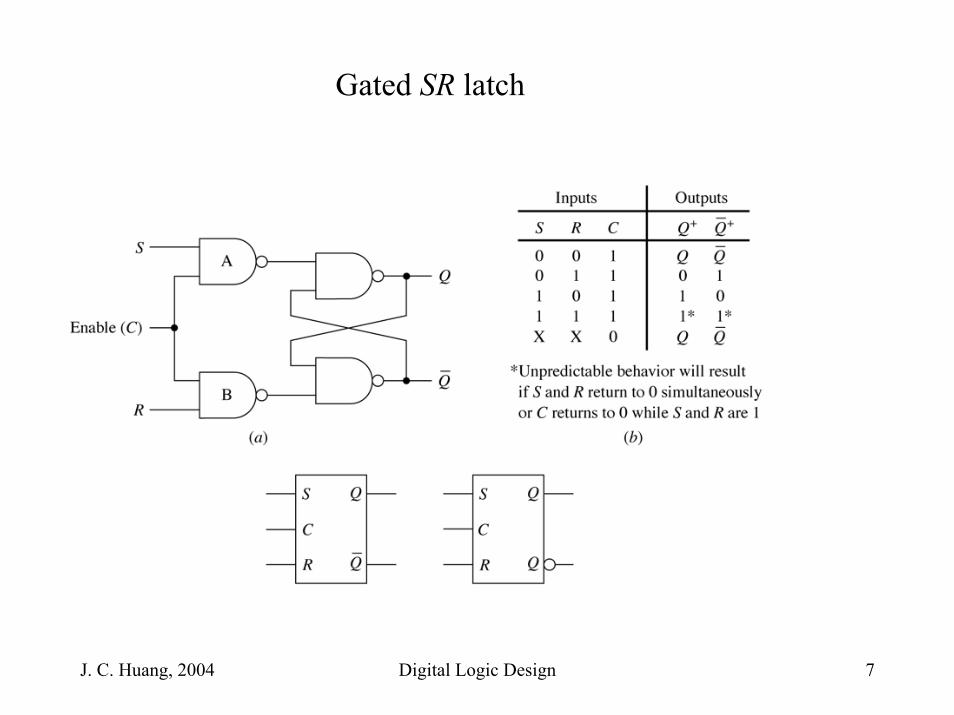
Gated SR latch

J. C. Huang, 2004 Digital Logic Design 8
Gated D latch

J. C. Huang, 2004 Digital Logic Design 9
Timing considerations
• Propagation delays• Minimum pulse width• Setup and hold time

J. C. Huang, 2004 Digital Logic Design 10
Propagation delay
The time it takes a change in the input signal to produce a change in the output signal.

J. C. Huang, 2004 Digital Logic Design 11
Minimum pulse width
The minimum amount of time a signal must be applied in order to produce a desired result.

J. C. Huang, 2004 Digital Logic Design 12
Setup and hold times
• To achieve a satisfactory operation of a gated latch, constraints are normally placed on the time intervals between input changes.
• The minimum time the input signal must be held fixed before and after the latching action is called the setup time and holdtime, respectively.
J. C. Huang, 2004 Digital Logic Design 13
JK- and T-type flip-flops
In addition to the SR-type and D-type flip-flops discussed above, there are two other types, viz., JK- and T-type flip-flops.

J. C. Huang, 2004 Digital Logic Design 14
D Q
Q
J
Q
K
JK flip-flop
Q
Clock
(a) Circuit
01
Q t( )0
00
Q t( )
J Q
QK
K 1+
(b) Truth table (c) Graphical symbol
J
0 111 Q t( )1

J. C. Huang, 2004 Digital Logic Design 15
JK flip-flops
A JK flip-flop works just like an SR flip-flop if we consider J input as S(et) input and K input as R(eset) input, except when both S and R inputs are set to 1, the output simply flips over.

J. C. Huang, 2004 Digital Logic Design 16
T-type flip-flops
A T flip-flop is obtained from a JK flip-flop by tying the J and K inputs together to form the T input.
J
K
Q
Q'C
T Q
Q'

J. C. Huang, 2004 Digital Logic Design 17
Flip-flops
• There are four different types of flip-flops: SR, D, JK, and T types.
• The properties of these flip-flops are summarized in the following 4 slides.
• The function and application tables are also known as characteristic and excitation tables, respectively.
J. C. Huang, 2004 Digital Logic Design 18
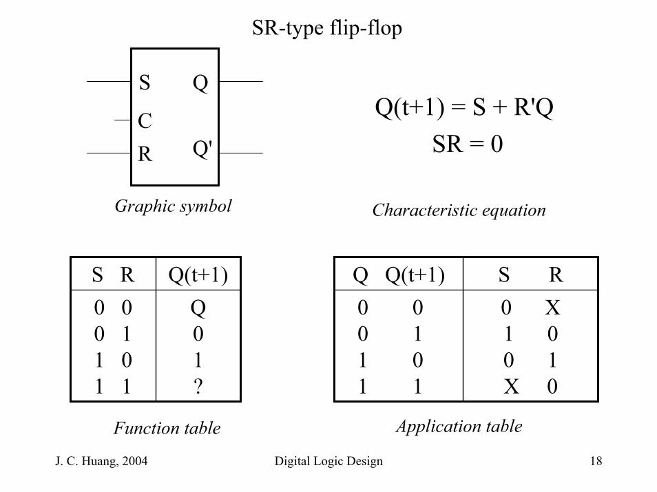
SR-type flip-flop
S Q
Q'CR
Q(t+1) = S + R'Q SR = 0
Graphic symbol Characteristic equation
Function table Application table
Q01?
0 00 11 01 1
Q(t+1)S R0 X1 00 1X 0
0 00 11 01 1
S RQ Q(t+1)

J. C. Huang, 2004 Digital Logic Design 19
D-type flip-flop
D Q
Q'C Q(t+1) = D
Graphic symbol Characteristic equation
0101
0 00 11 01 1
DQ Q(t+1)
01
01
Q(t+1)D
Function tableApplication table

J. C. Huang, 2004 Digital Logic Design 20
JK-type flip-flop
J
K
Q
Q'C
Q(t+1) = JQ' + K'Q
Graphic symbol Characteristic equation
Function table Application table
Q01Q'
0 00 11 01 1
Q(t+1)J K0 X1 XX 1X 0
0 00 11 01 1
J KQ Q(t+1)

J. C. Huang, 2004 Digital Logic Design 21
T-type flip-flop
T Q
Q'C Q(t+1) = TQ' + T'Q
Graphic symbol Characteristic equation
0110
0 00 11 01 1
TQ Q(t+1)
QQ'
01
Q(t+1)T
Function tableApplication table

J. C. Huang, 2004 Digital Logic Design 22
Positive and negative edge
• The transition of a control signal (clock pulse) from its low to high value (0 to 1) in positive logic is called the positive edge of the control signal, while the transition from high to low (1 to 0) is called the negative edge.

J. C. Huang, 2004 Digital Logic Design 23
Edge-triggered flip-flops
• Edge triggered flip-flops use just one of the edges of the clock pulse to affect the reading of the input lines.
• These flip-flops are designed to be triggered by either the positive or negative edge.
• In analyzing the behavior of an asynchronous sequential circuit, one often needs to know which edge trigger the flip-flops used.

J. C. Huang, 2004 Digital Logic Design 24
D Q
Q
D Q
Q
D Q
Q
Clk
D level sensitive latchQ a
Q a Clock
positive-edge-triggered
Q b
Q b
Q c
Q c negative-edge-triggered
(a) Circuit
Clock
D
Q a
Q b
Q c
(b) Timing diagram

J. C. Huang, 2004 Digital Logic Design 25
Serial-in, serial-out unidirectional shift register
J. C. Huang, 2004 Digital Logic Design 26
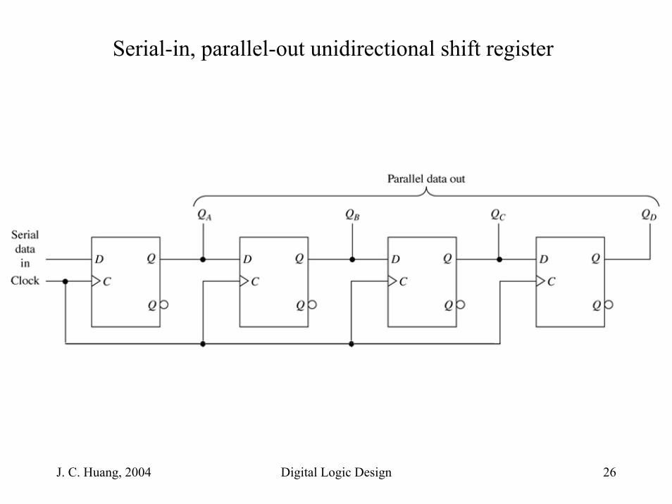
Serial-in, parallel-out unidirectional shift register
J. C. Huang, 2004 Digital Logic Design 27
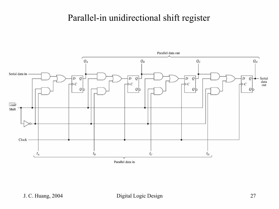
Parallel-in unidirectional shift register
J. C. Huang, 2004 Digital Logic Design 28
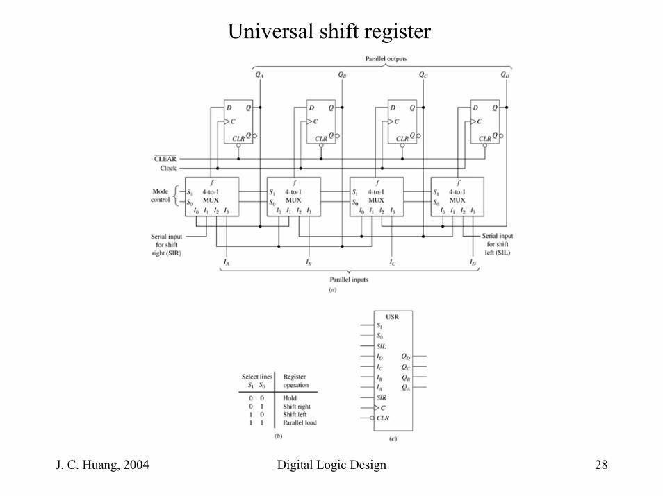
Universal shift register

J. C. Huang, 2004 Digital Logic Design 29
4-bit binary ripple (asynchronous) counter with positive-edge triggeredflip-flops.
J. C. Huang, 2004 Digital Logic Design 30
T Q
Q
T Q
Q
T Q
Q
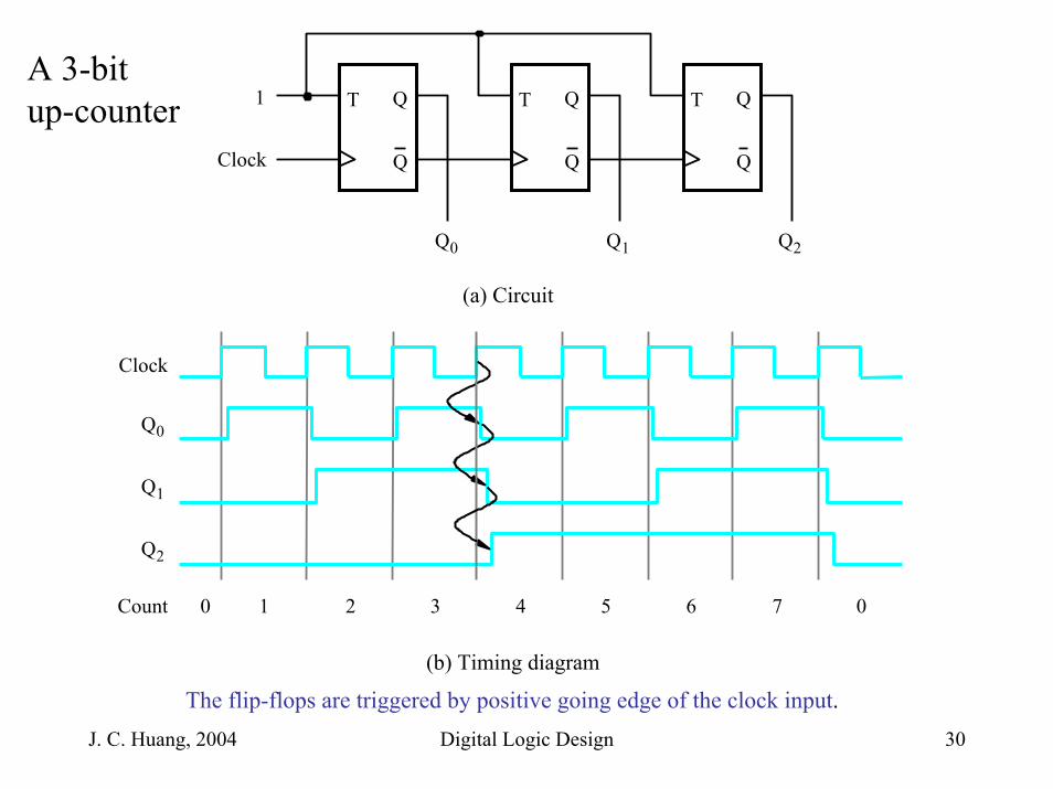
A 3-bitup-counter 1
Clock
Q 0 Q 1 Q 2
(a) Circuit
Clock
Q 0
Q 1
Q 2
Count 0 1 2 3 4 5 6 7 0
(b) Timing diagram
The flip-flops are triggered by positive going edge of the clock input.

J. C. Huang, 2004 Digital Logic Design 31
Analysis method:
Construct a list of state changes as follows.
1. Assume that the counter starts with some values, say, 000.
2. Because T=1 for Q0, Q0 will change at the arrival of every clock pulse.Complete the listing for Q0.
3. Because T=Q0’, and because the flip-flop is triggered by a positive going clock input, for Q1, Q1 changes its content whenever Q0 changes from 1 to 0.
4. Do the same for the listing for Q2.
Q2 Q1 Q0
0 0 00 0 10 1 00 1 11 0 01 0 11 1 01 1 10 0 0

J. C. Huang, 2004 Digital Logic Design 32
T Q
Q
T Q
Q
T Q
Q
1
Clock
A 3-bitdown-counter
Q 0 Q 1 Q 2
(a) Circuit
Clock
Q 0
Q 1
Q 2
Count 0 7 6 5 4 3 2 1 0
(b) Timing diagram
The flip-flops are triggered by positive going edge of the clock input

J. C. Huang, 2004 Digital Logic Design 33
Analysis method:
Construct a list of state changes as follows.
1. Assume that the counter starts with some values, say, 000.
2. Because T=1 for Q0, Q0 will change at the arrival of every clock pulse.Complete the listing for Q0.
3. Because T=Q0, and because the flip-flop is triggered by a positive going clock input, for Q1, it changes its content whenever Q0 changes from 0 to 1.
4. Do the same for the listing for Q2.
Q2 Q1 Q0
0 0 01 1 11 1 01 0 11 0 00 1 10 1 00 0 10 0 0
J. C. Huang, 2004 Digital Logic Design 34
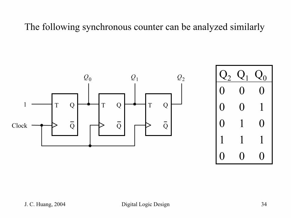
The following synchronous counter can be analyzed similarly
0 0 00 0 10 1 01 1 10 0 0
Q2 Q1 Q0
T Q
Q
1 T Q
Q
T Q
Q
Q 0 Q 1 Q 2
Clock

J. C. Huang, 2004 Digital Logic Design 35
Four-bit synchronous binary counter

J. C. Huang, 2004 Digital Logic Design 36
Four-bit synchronous binary counter variation

J. C. Huang, 2004 Digital Logic Design 37
Four-bit synchronous binary counter with parallel load inputs

J. C. Huang, 2004 Digital Logic Design 38
Synchronous mod-10 counter
J. C. Huang, 2004 Digital Logic Design 39
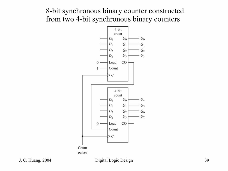
8-bit synchronous binary counter constructed from two 4-bit synchronous binary counters

J. C. Huang, 2004 Digital Logic Design 40
Mod-4 ring counter

J. C. Huang, 2004 Digital Logic Design 41
Mod-8 twisted-ring counter (or Johnson counter)
J. C. Huang, 2004 Digital Logic Design 42
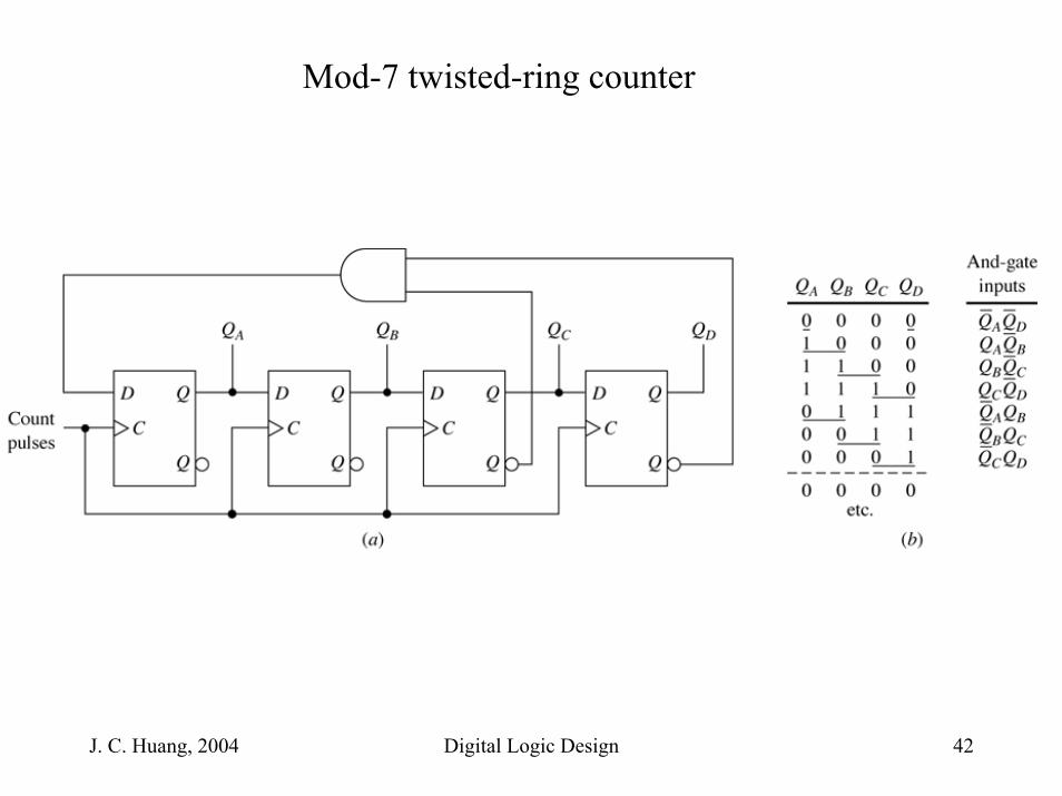
Mod-7 twisted-ring counter
J. C. Huang, 2004 Digital Logic Design 43
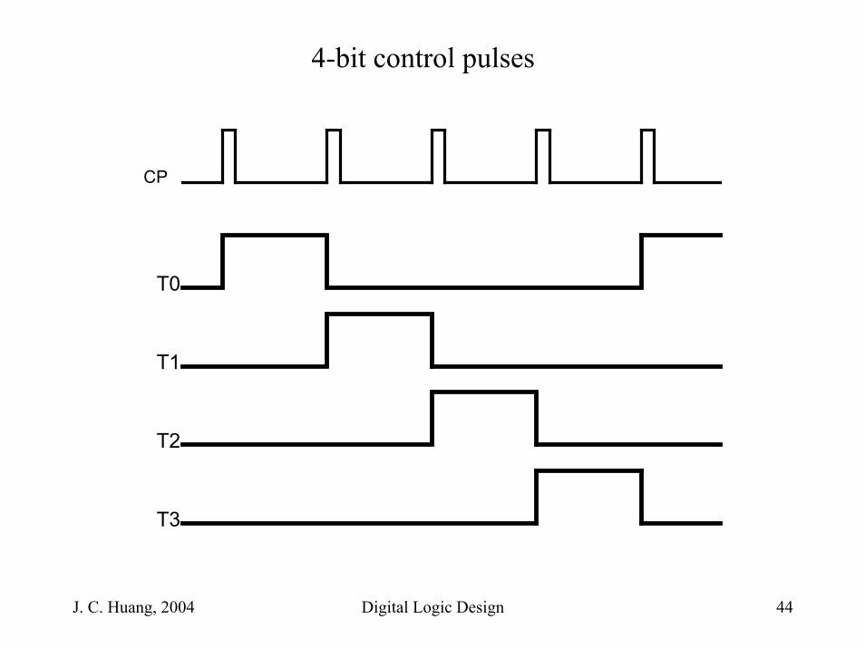
Control signal generators
• A control signal generator is a sequential circuit that generate a sequence of bit patterns, each of which contains only one 1. It is used to activate various devices in turn.
• Shown in the next slide are the wave forms of 4-bit control signals.
J. C. Huang, 2004 Digital Logic Design 44
4-bit control pulses
T0
T1
T2
T3
CP
J. C. Huang, 2004 Digital Logic Design 45
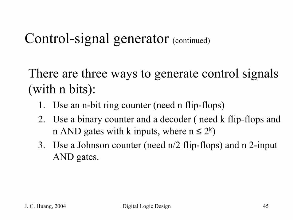
Control-signal generator (continued)
There are three ways to generate control signals (with n bits):
1. Use an n-bit ring counter (need n flip-flops)2. Use a binary counter and a decoder ( need k flip-flops and
n AND gates with k inputs, where n ≤ 2k)3. Use a Johnson counter (need n/2 flip-flops) and n 2-input
AND gates.

J. C. Huang, 2004 Digital Logic Design 46
w 0 En
y 0
w 1
y 1 y 2 y 3
T 1 T 2 T 3
2-to-4 decoder
T 0
A part of the control circuit for the processor
Reset Up-counterQ 1 Q 0
1
Clock
Clear
J. C. Huang, 2004 Digital Logic Design 47
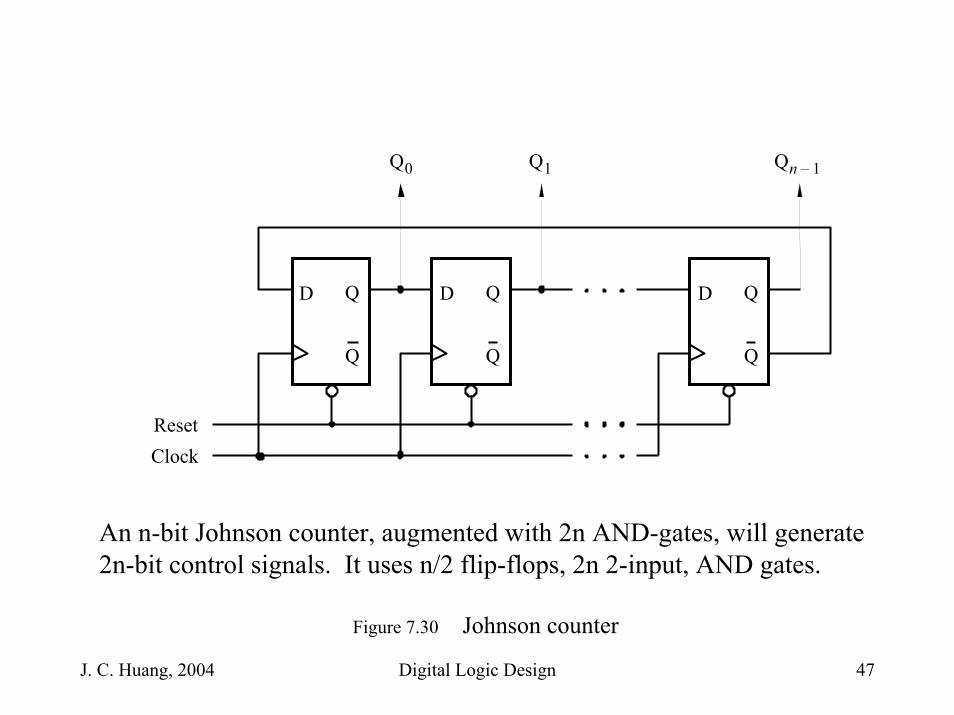
Q 1 Q n –Q 0 1
D Q
Q
D Q
Q
D Q
Q
Reset Clock
An n-bit Johnson counter, augmented with 2n AND-gates, will generate2n-bit control signals. It uses n/2 flip-flops, 2n 2-input, AND gates.
Figure 7.30 Johnson counter

J. C. Huang, 2004 Digital Logic Design 48
A B C
D Q
Q
D Q
Q
D Q
Q
Reset Clock
Figure 7.30 A 3-bit Johnson counter
J. C. Huang, 2004 Digital Logic Design 49
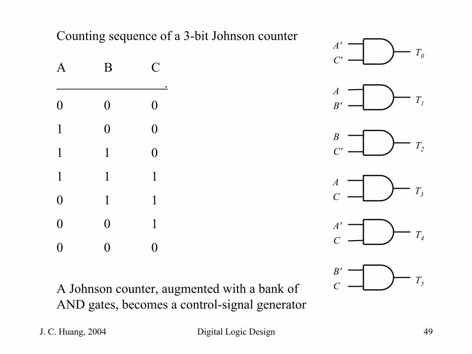
Counting sequence of a 3-bit Johnson counter
A B C.
0 0 0
1 0 0
1 1 0
1 1 1
0 1 1
0 0 1
0 0 0
A Johnson counter, augmented with a bank ofAND gates, becomes a control-signal generator
A' C'
T0
AB' T1
BC' T2
AC T3
A' C T4
B' C T5

J. C. Huang, 2004 Digital Logic Design 50
Synchronous counters
A synchronous counter is a special kind of synchronous sequential circuit, the analysis and design of such a circuit will be discussed in the next chapter.