Embed Size (px)
Citation preview

1
Chapter 9 Cascode Stages and Current Mirros
Microelectronics, 2nd edition by Behzad Razavi
CH 9 Cascode Stages and Current Mirrors 2
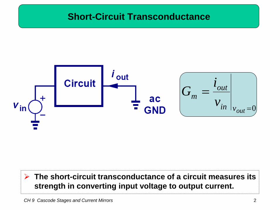
Short-Circuit Transconductance
The short-circuit transconductance of a circuit measures its strength in converting input voltage to output current.
0=
=outvin
outm v
iG
CH 9 Cascode Stages and Current Mirrors 3
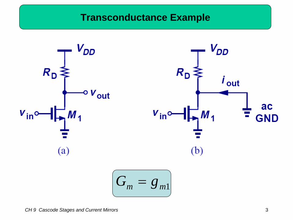
Transconductance Example
1mm gG =
CH 9 Cascode Stages and Current Mirrors 4
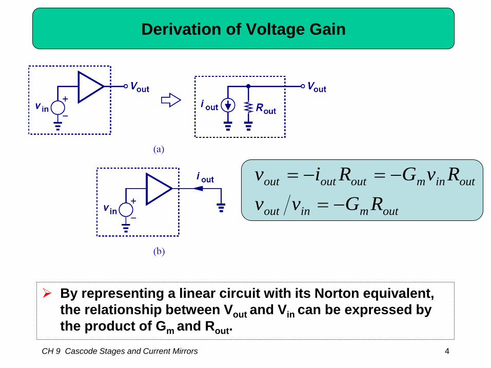
Derivation of Voltage Gain
By representing a linear circuit with its Norton equivalent, the relationship between Vout and Vin can be expressed by the product of Gm and Rout.
outminout
outinmoutoutout
RGvvRvGRiv
−=−=−=
CH 9 Cascode Stages and Current Mirrors 5
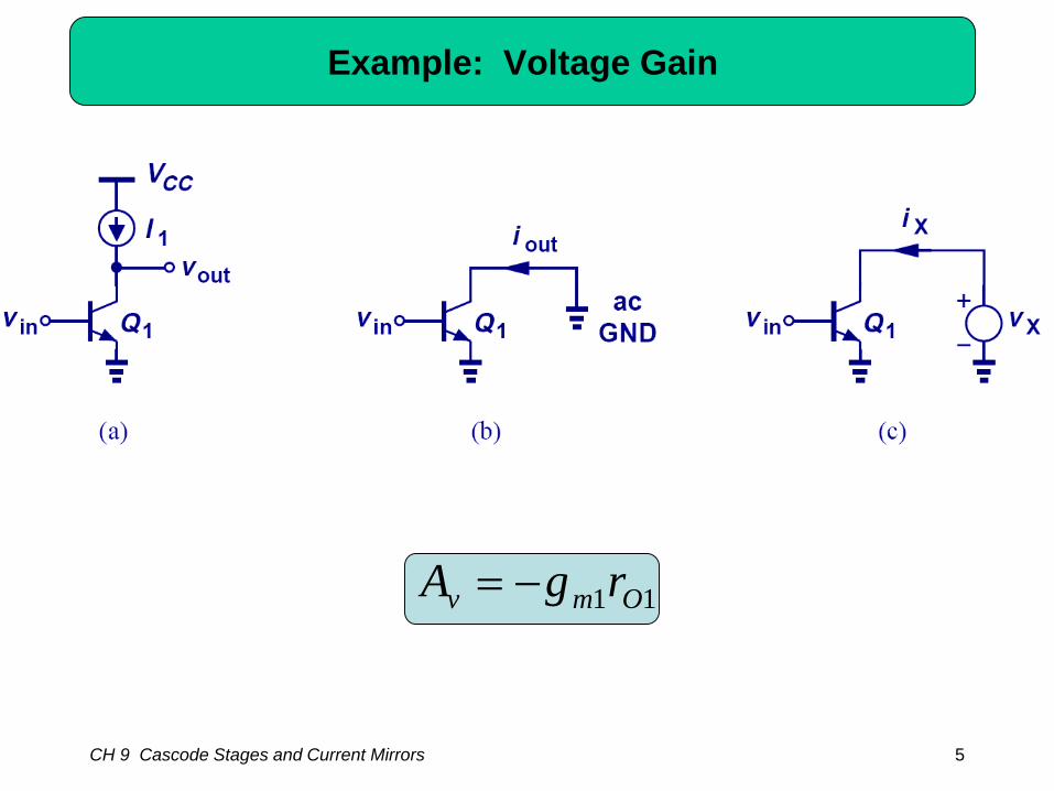
Example: Voltage Gain
11 Omv rgA −=

6
Chapter 10 Differential Amplifiers
Microelectronics, 2nd edition by Behzad Razavi
CH 10 Differential Amplifiers 7
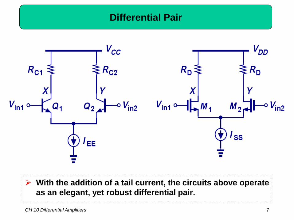
Differential Pair
With the addition of a tail current, the circuits above operate as an elegant, yet robust differential pair.
CH 10 Differential Amplifiers 8
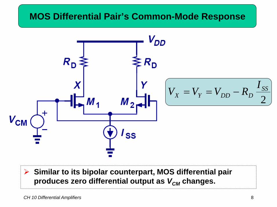
MOS Differential Pair’s Common-Mode Response
Similar to its bipolar counterpart, MOS differential pair produces zero differential output as VCM changes.
2SS
DDDYXIRVVV −==
CH 10 Differential Amplifiers 9
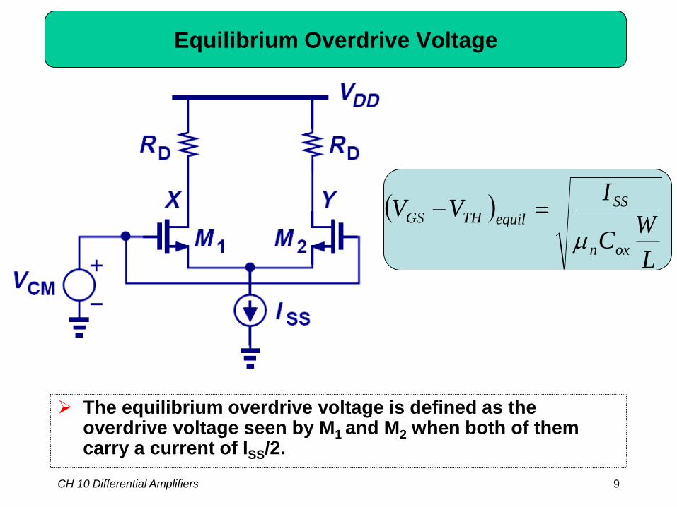
Equilibrium Overdrive Voltage
The equilibrium overdrive voltage is defined as the overdrive voltage seen by M1 and M2 when both of them carry a current of ISS/2.
( )
LWC
IVVoxn
SSequilTHGS
µ=−
CH 10 Differential Amplifiers 10
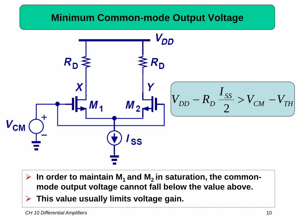
Minimum Common-mode Output Voltage
In order to maintain M1 and M2 in saturation, the common-mode output voltage cannot fall below the value above.
This value usually limits voltage gain.
THCMSS
DDD VVIRV −>−2
CH 10 Differential Amplifiers 11
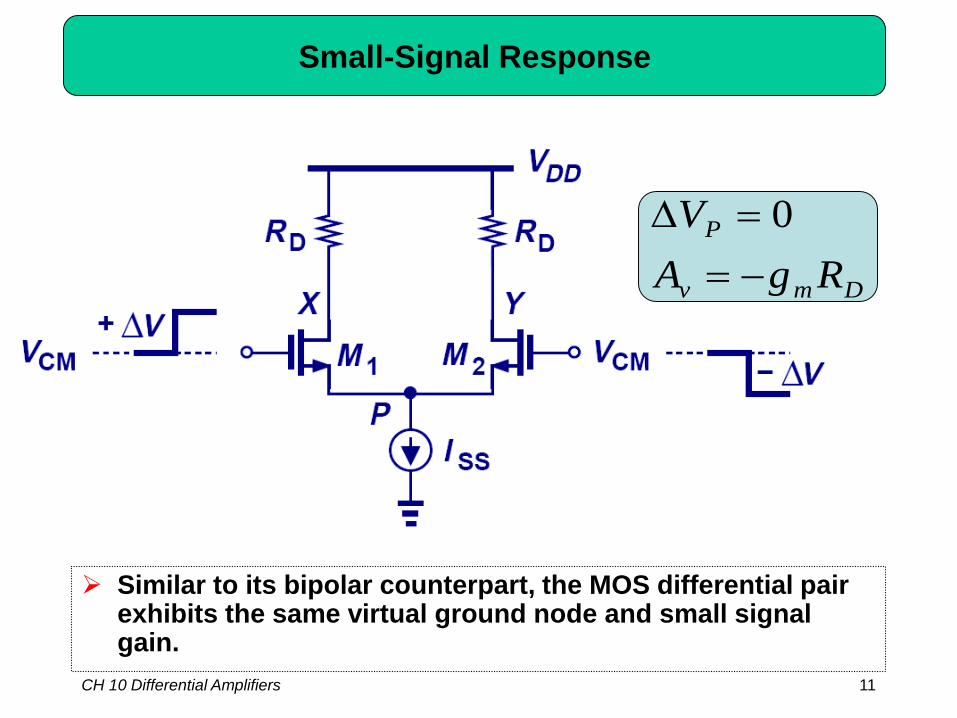
Small-Signal Response
Similar to its bipolar counterpart, the MOS differential pair exhibits the same virtual ground node and small signal gain.
Dmv
P
RgAV
−==∆ 0
CH 10 Differential Amplifiers 12
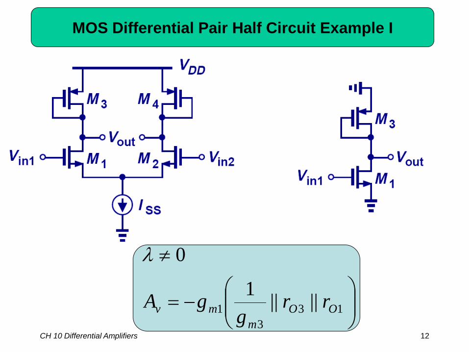
MOS Differential Pair Half Circuit Example I
−=
≠
133
1 ||||1
0
OOm
mv rrg
gA
λ
CH 10 Differential Amplifiers 13
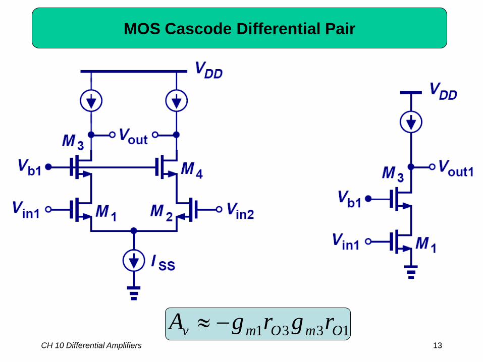
MOS Cascode Differential Pair
1331 OmOmv rgrgA −≈
CH 10 Differential Amplifiers 14
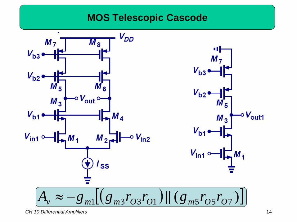
MOS Telescopic Cascode
( )[ ])(|| 7551331 OOmOOmmv rrgrrggA −≈
CH 10 Differential Amplifiers 15
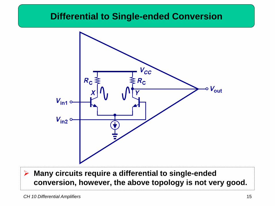
Differential to Single-ended Conversion
Many circuits require a differential to single-ended conversion, however, the above topology is not very good.
CH 10 Differential Amplifiers 16
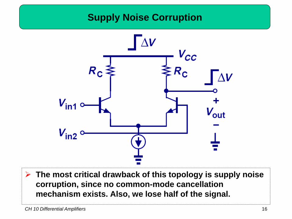
Supply Noise Corruption
The most critical drawback of this topology is supply noise corruption, since no common-mode cancellation mechanism exists. Also, we lose half of the signal.
CH 10 Differential Amplifiers 17
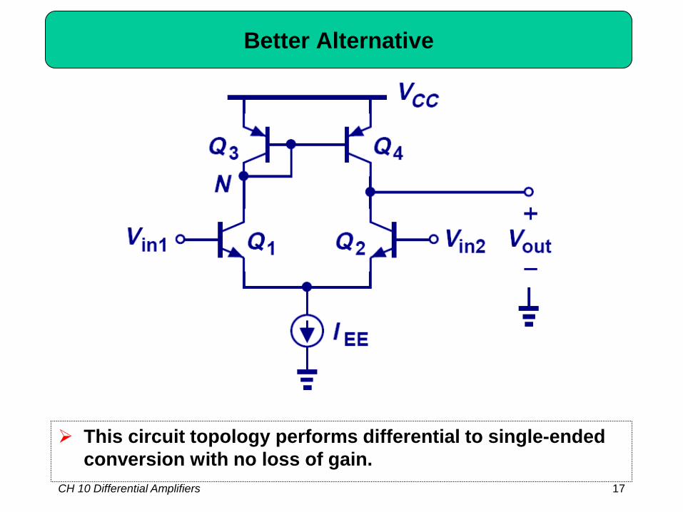
Better Alternative
This circuit topology performs differential to single-ended conversion with no loss of gain.
CH 10 Differential Amplifiers 18
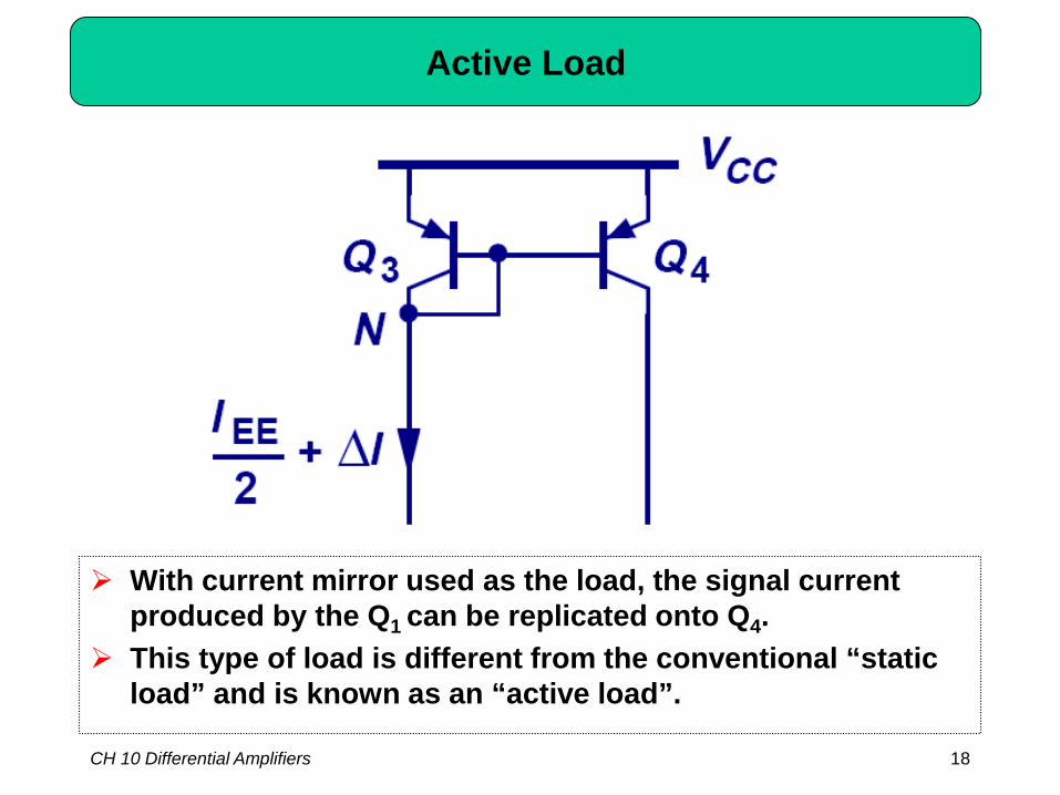
Active Load
With current mirror used as the load, the signal current produced by the Q1 can be replicated onto Q4.
This type of load is different from the conventional “static load” and is known as an “active load”.
CH 10 Differential Amplifiers 19
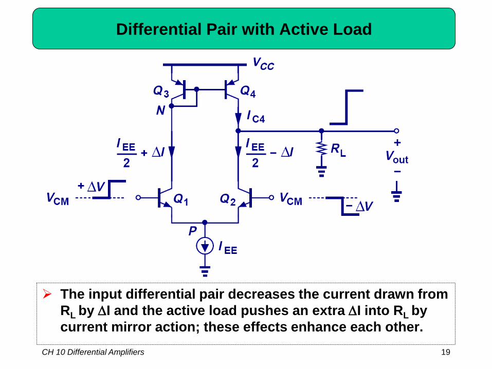
Differential Pair with Active Load
The input differential pair decreases the current drawn from RL by ∆I and the active load pushes an extra ∆I into RL by current mirror action; these effects enhance each other.
CH 10 Differential Amplifiers 20
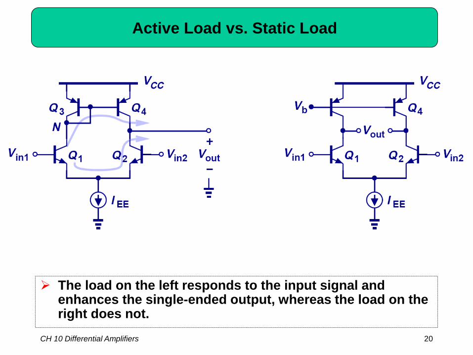
Active Load vs. Static Load
The load on the left responds to the input signal and enhances the single-ended output, whereas the load on the right does not.
CH 10 Differential Amplifiers 21
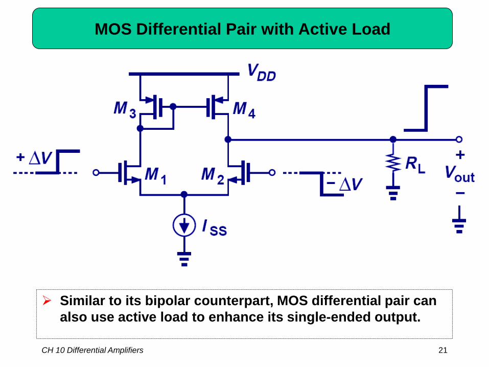
MOS Differential Pair with Active Load
Similar to its bipolar counterpart, MOS differential pair can also use active load to enhance its single-ended output.
CH 10 Differential Amplifiers 22
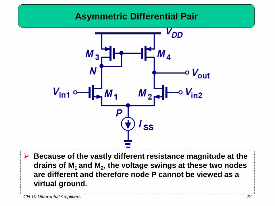
Asymmetric Differential Pair
Because of the vastly different resistance magnitude at the drains of M1 and M2, the voltage swings at these two nodes are different and therefore node P cannot be viewed as a virtual ground.
23
Chapter 11 Frequency Response
Microelectronics, 2nd edition by Behzad Razavi
CH 11 Frequency Response 24
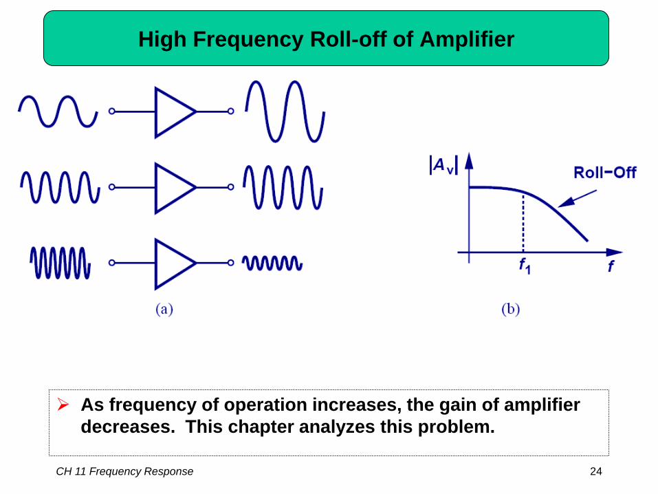
High Frequency Roll-off of Amplifier
As frequency of operation increases, the gain of amplifier decreases. This chapter analyzes this problem.
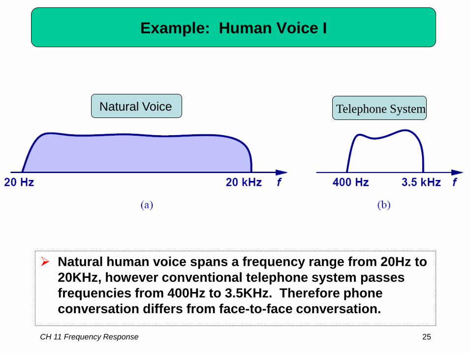
Example: Human Voice I
Natural human voice spans a frequency range from 20Hz to 20KHz, however conventional telephone system passes frequencies from 400Hz to 3.5KHz. Therefore phone conversation differs from face-to-face conversation.
CH 11 Frequency Response 25
Natural Voice Telephone System
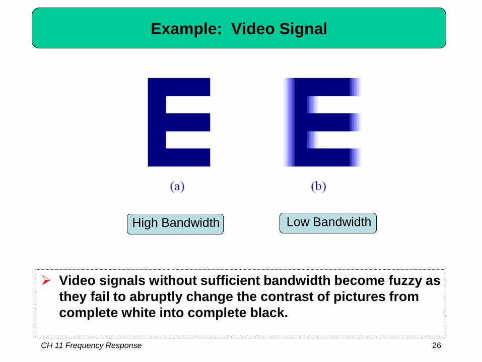
Example: Video Signal
Video signals without sufficient bandwidth become fuzzy as they fail to abruptly change the contrast of pictures from complete white into complete black.
CH 11 Frequency Response 26
High Bandwidth Low Bandwidth
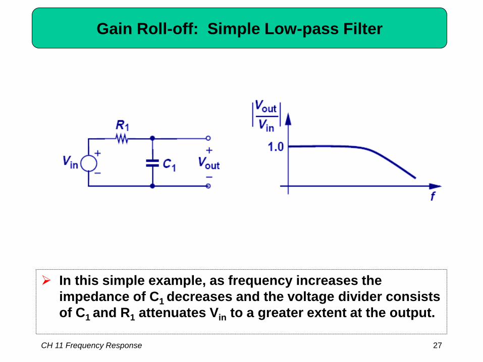
Gain Roll-off: Simple Low-pass Filter
In this simple example, as frequency increases the impedance of C1 decreases and the voltage divider consists of C1 and R1 attenuates Vin to a greater extent at the output.
CH 11 Frequency Response 27
CH 11 Frequency Response 28
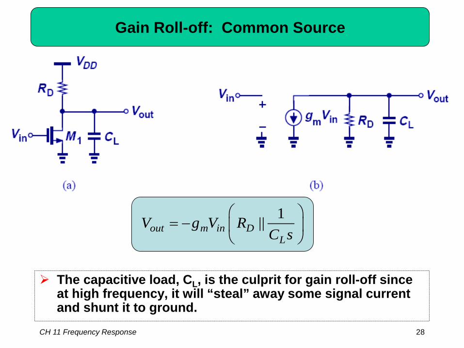
Gain Roll-off: Common Source
The capacitive load, CL, is the culprit for gain roll-off since at high frequency, it will “steal” away some signal current and shunt it to ground.
1||out m in DL
V g V RC s
= −
CH 11 Frequency Response 29
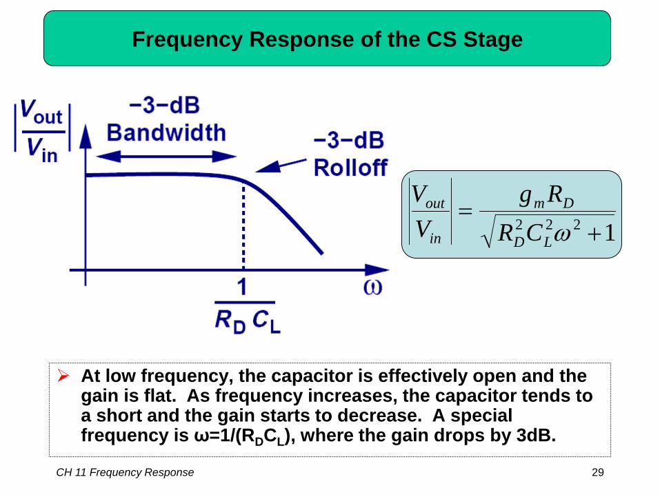
Frequency Response of the CS Stage
At low frequency, the capacitor is effectively open and the gain is flat. As frequency increases, the capacitor tends to a short and the gain starts to decrease. A special frequency is ω=1/(RDCL), where the gain drops by 3dB.
1222 +=
ωLD
Dm
in
out
CRRg
VV
CH 11 Frequency Response 30
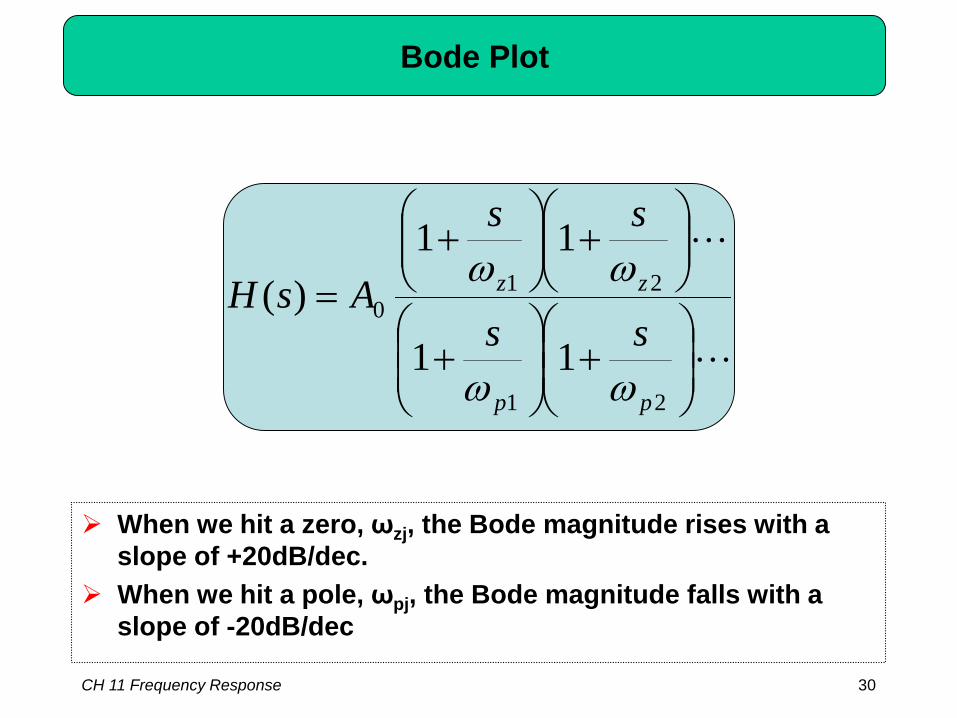
Bode Plot
When we hit a zero, ωzj, the Bode magnitude rises with a slope of +20dB/dec.
When we hit a pole, ωpj, the Bode magnitude falls with a slope of -20dB/dec
+
+
+
+
=
21
210
11
11)(
pp
zz
ss
ss
AsH
ωω
ωω
CH 11 Frequency Response 31
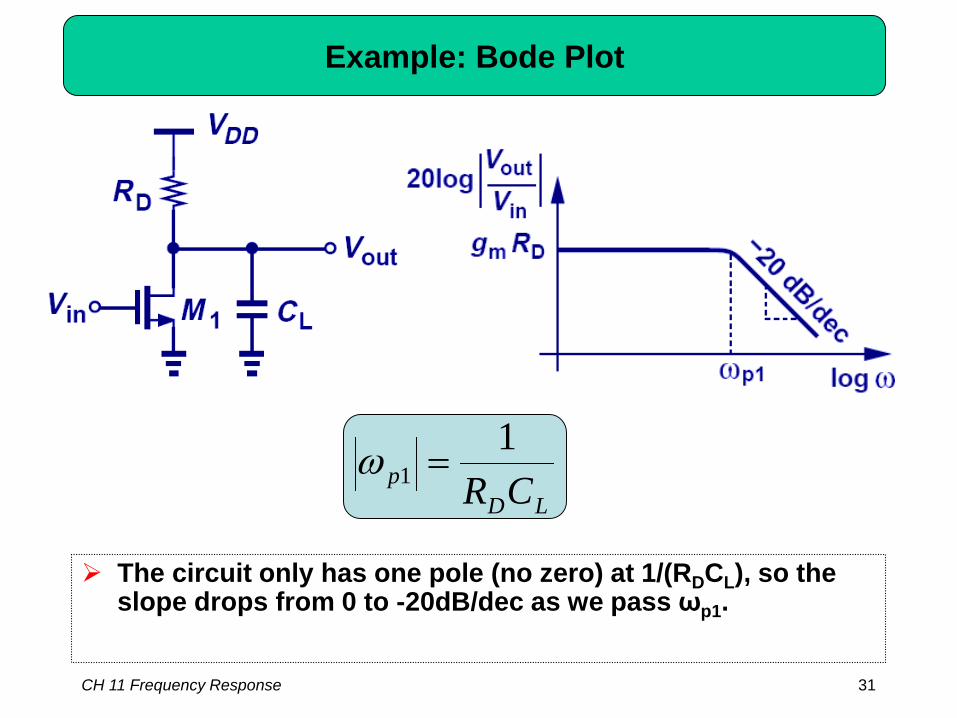
Example: Bode Plot
The circuit only has one pole (no zero) at 1/(RDCL), so the slope drops from 0 to -20dB/dec as we pass ωp1.
LDp CR
11 =ω
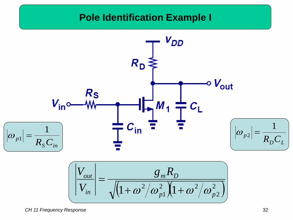
CH 11 Frequency Response 32
Pole Identification Example I
inSp CR
11 =ω
LDp CR
12 =ω
( )( )22
221
2 11 pp
Dm
in
out RgVV
ωωωω ++=
CH 11 Frequency Response 33
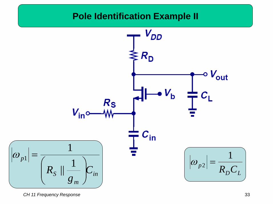
Pole Identification Example II
inm
S
p
Cg
R
=
1||
11ω
LDp CR
12 =ω
CH 11 Frequency Response 34
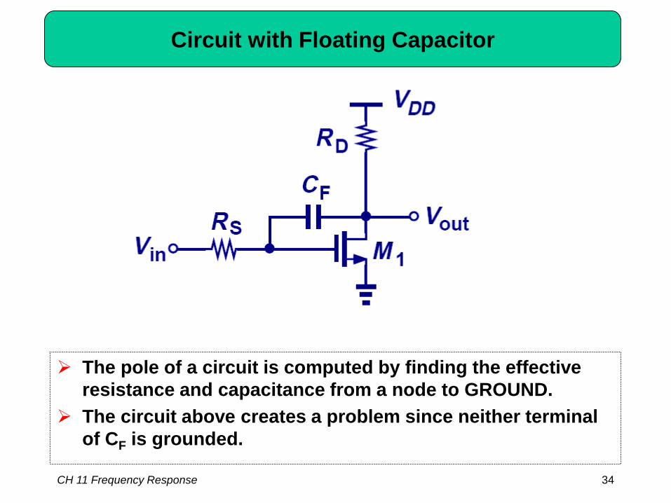
Circuit with Floating Capacitor
The pole of a circuit is computed by finding the effective resistance and capacitance from a node to GROUND.
The circuit above creates a problem since neither terminal of CF is grounded.
CH 11 Frequency Response 35
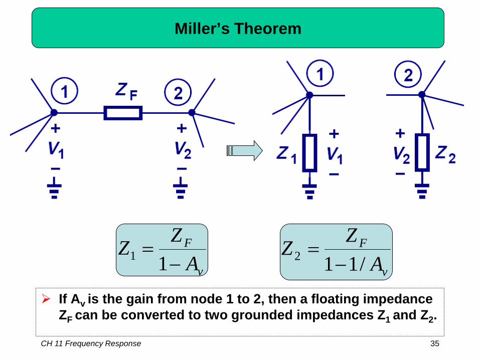
Miller’s Theorem
If Av is the gain from node 1 to 2, then a floating impedance ZF can be converted to two grounded impedances Z1 and Z2.
v
F
AZZ−
=11
v
F
AZZ
/112 −=
CH 11 Frequency Response 36
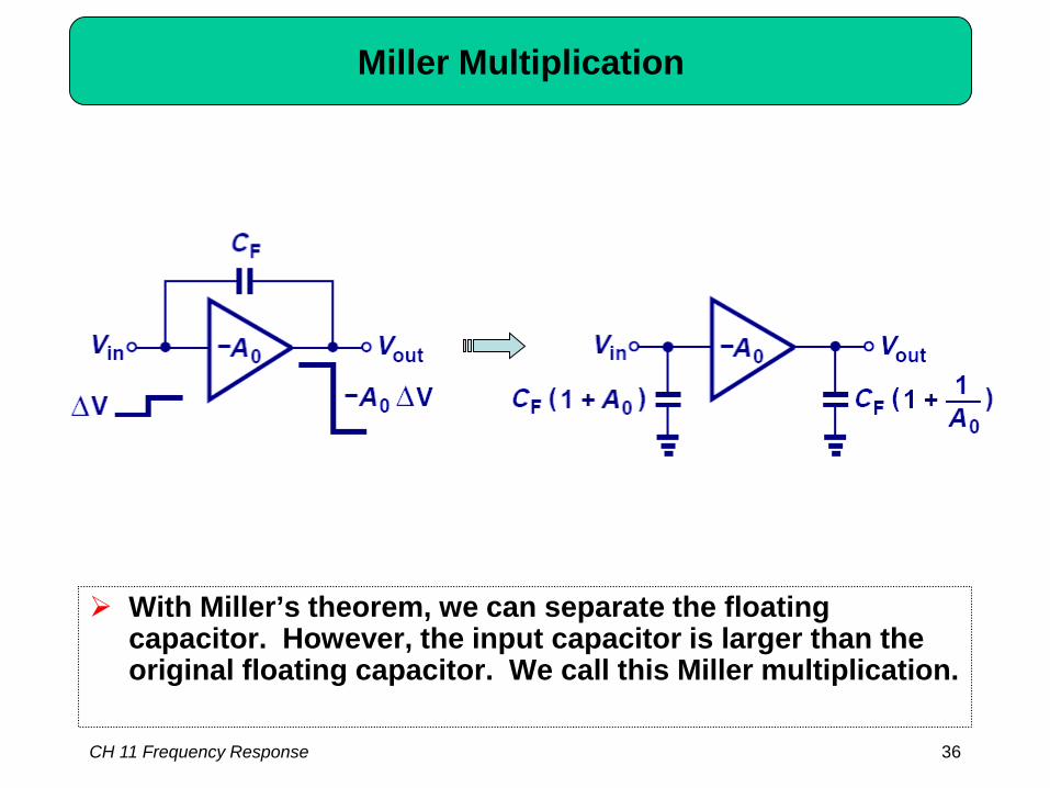
Miller Multiplication
With Miller’s theorem, we can separate the floating capacitor. However, the input capacitor is larger than the original floating capacitor. We call this Miller multiplication.
CH 11 Frequency Response 37
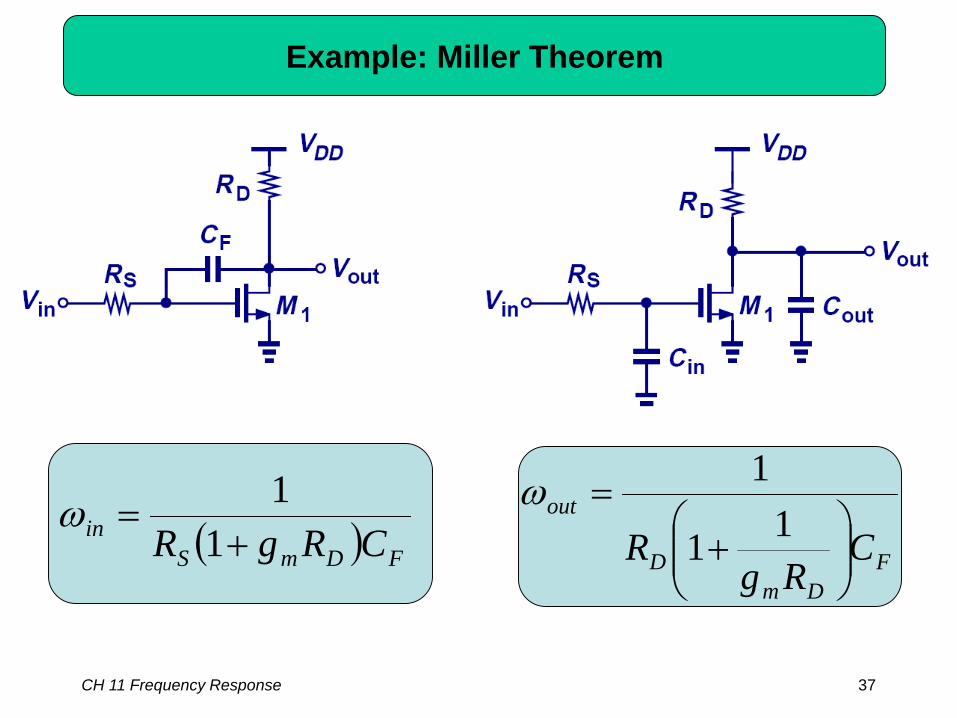
Example: Miller Theorem
( ) FDmSin CRgR +=
11ω
FDm
D
out
CRg
R
+
=11
1ω
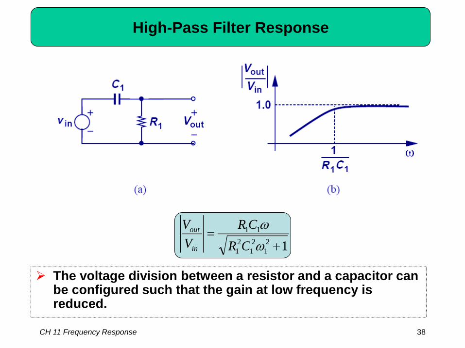
High-Pass Filter Response
121
21
21
11
+=
ωω
CRCR
VV
in
out
The voltage division between a resistor and a capacitor can be configured such that the gain at low frequency is reduced.
CH 11 Frequency Response 38
CH 11 Frequency Response 39
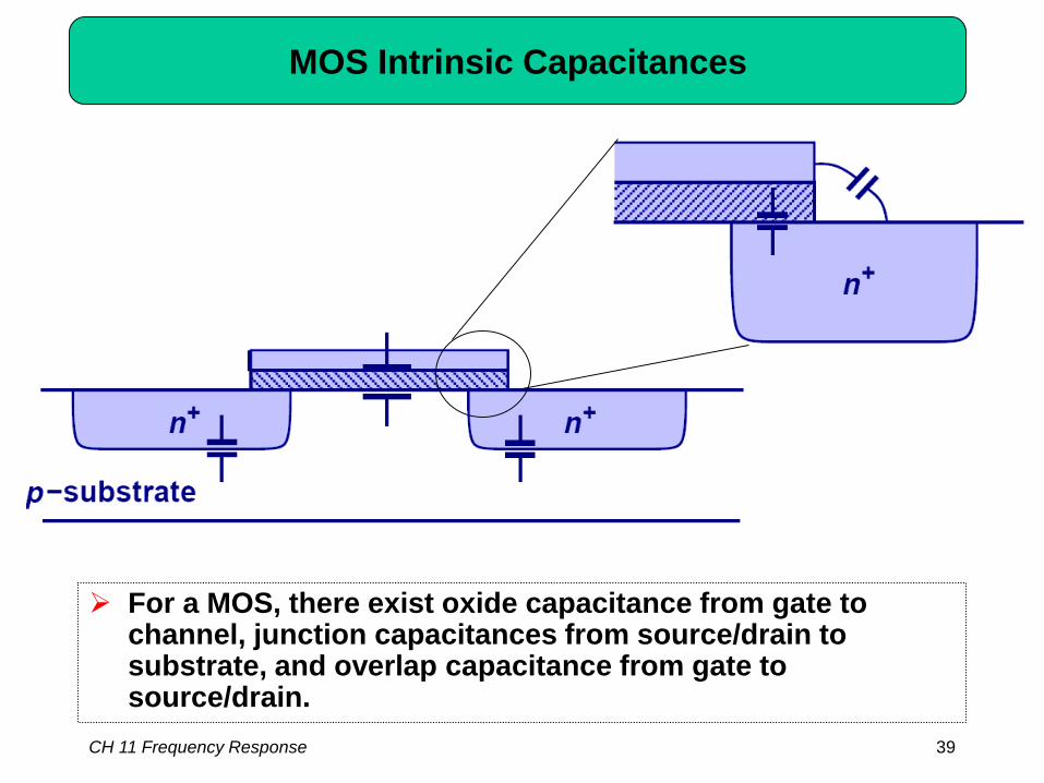
MOS Intrinsic Capacitances
For a MOS, there exist oxide capacitance from gate to channel, junction capacitances from source/drain to substrate, and overlap capacitance from gate to source/drain.
CH 11 Frequency Response 40
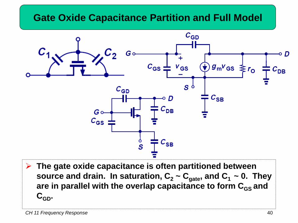
Gate Oxide Capacitance Partition and Full Model
The gate oxide capacitance is often partitioned between source and drain. In saturation, C2 ~ Cgate, and C1 ~ 0. They are in parallel with the overlap capacitance to form CGS and CGD.
CH 11 Frequency Response 41
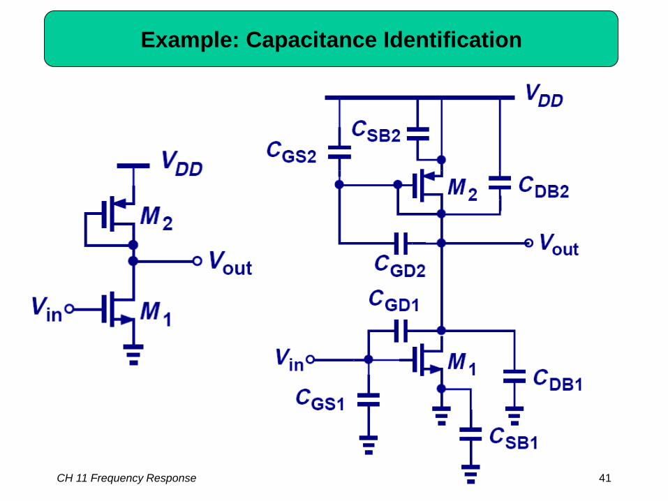
Example: Capacitance Identification
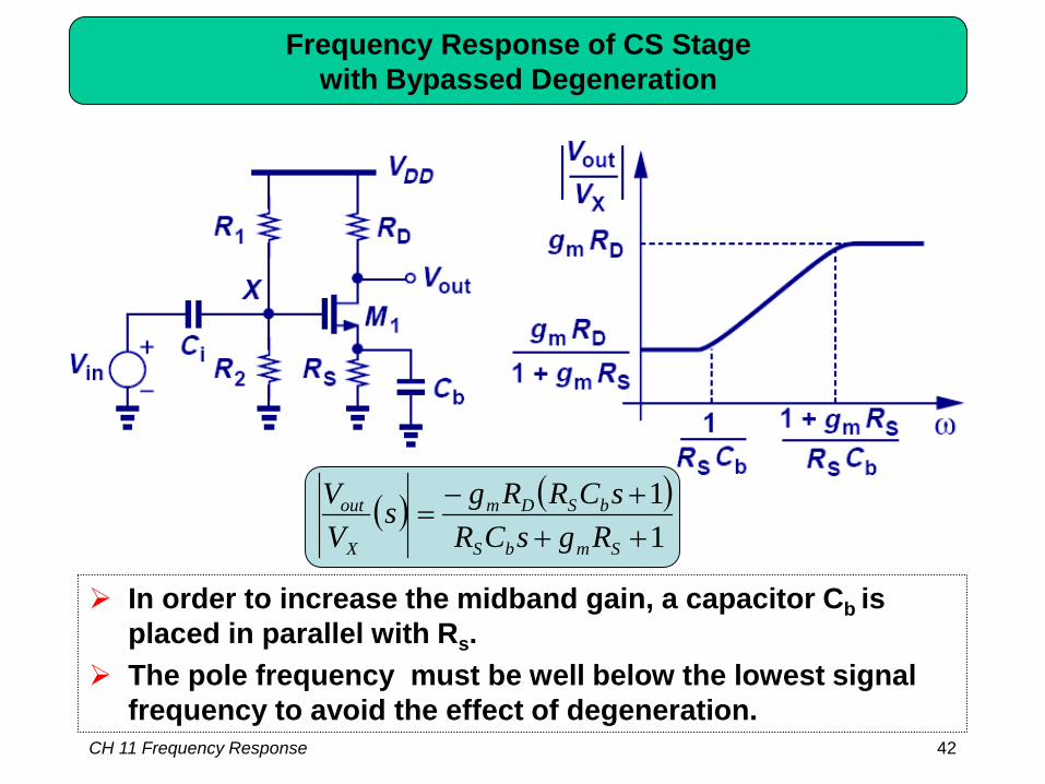
Frequency Response of CS Stagewith Bypassed Degeneration
( ) ( )11
+++−
=SmbS
bSDm
X
out
RgsCRsCRRgs
VV
In order to increase the midband gain, a capacitor Cb is placed in parallel with Rs.
The pole frequency must be well below the lowest signal frequency to avoid the effect of degeneration.
CH 11 Frequency Response 42
CH 11 Frequency Response 43
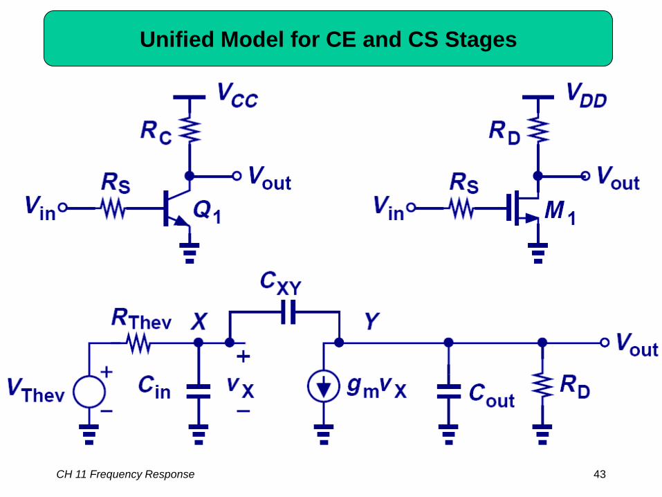
Unified Model for CE and CS Stages
CH 11 Frequency Response 44
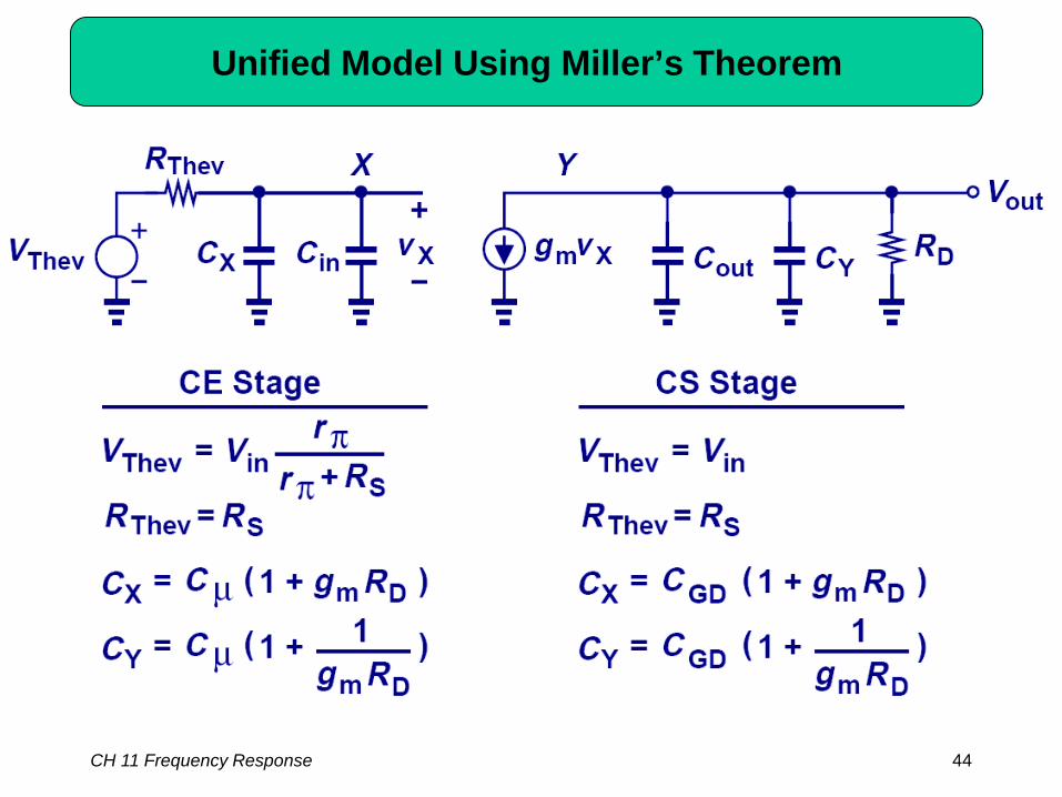
Unified Model Using Miller’s Theorem
CH 11 Frequency Response 45
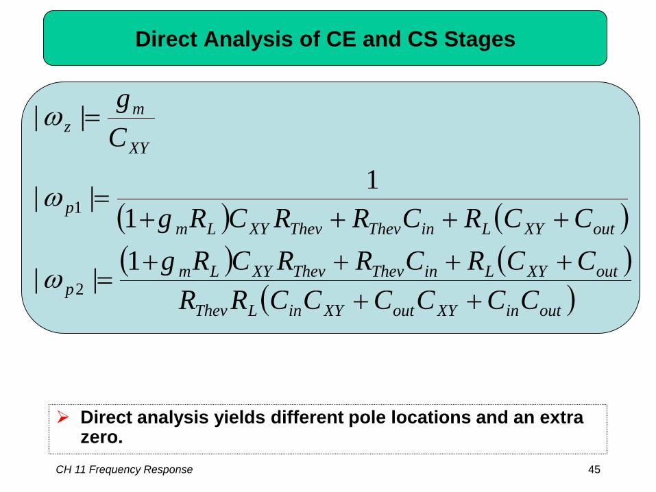
Direct Analysis of CE and CS Stages
Direct analysis yields different pole locations and an extra zero.
( ) ( )( ) ( )
( )outinXYoutXYinLThev
outXYLinThevThevXYLmp
outXYLinThevThevXYLmp
XY
mz
CCCCCCRRCCRCRRCRgCCRCRRCRg
Cg
++++++
=
++++=
=
1||
11||
||
2
1
ω
ω
ω
CH 11 Frequency Response 46
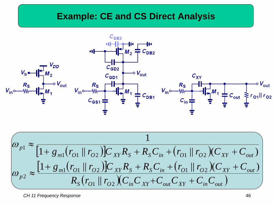
Example: CE and CS Direct Analysis
( )[ ] ( )( )[ ] ( )
( )( )outinXYoutXYinOOS
outXYOOinSSXYOOmp
outXYOOinSSXYOOmp
CCCCCCrrRCCrrCRRCrrgCCrrCRRCrrg
++++++
≈
++++≈
21
212112
212111
||)(||||1)(||||1
1
ω
ω
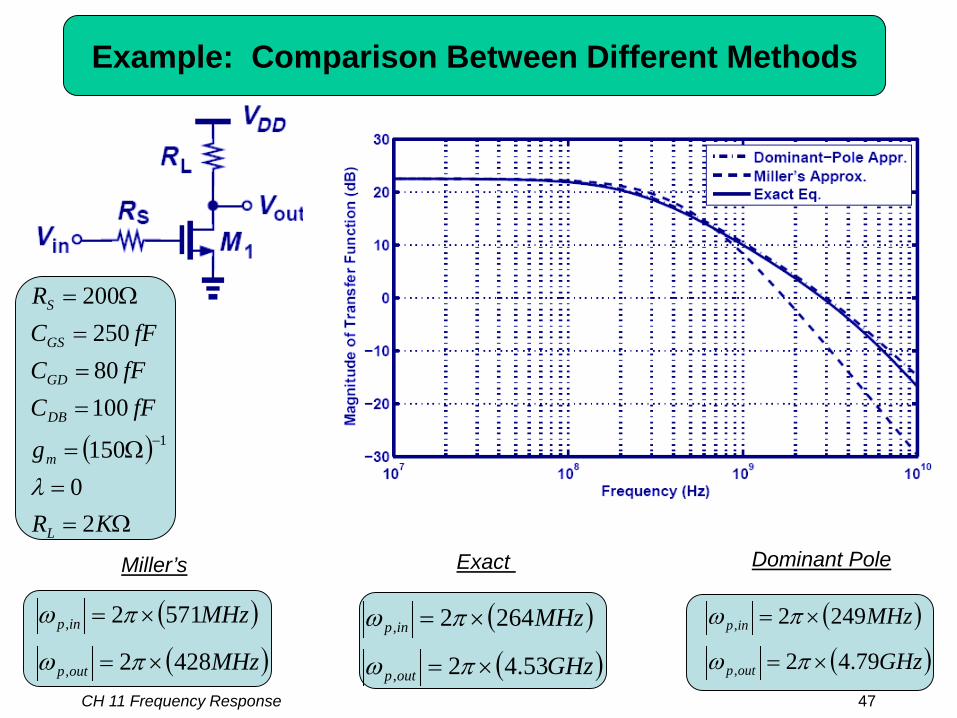
Example: Comparison Between Different Methods
( )( )MHz
MHz
outp
inp
4282
5712
,
,
×=
×=
πω
πω ( )( )GHz
MHz
outp
inp
53.42
2642
,
,
×=
×=
πω
πω ( )( )GHz
MHz
outp
inp
79.42
2492
,
,
×=
×=
πω
πω
( )
Ω==
Ω=
===
Ω=
−
KR
g
fFCfFCfFC
R
L
m
DB
GD
GS
S
20
150
10080250
200
1
λ
Miller’s Exact Dominant Pole
CH 11 Frequency Response 47
CH 11 Frequency Response 48
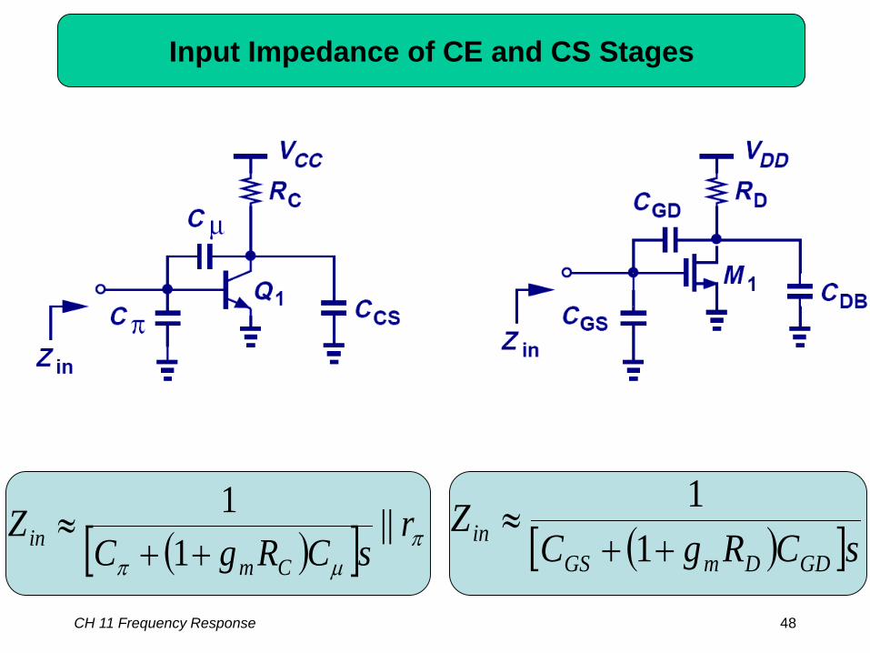
Input Impedance of CE and CS Stages
( )[ ] πµπ
rsCRgC
ZCm
in ||1
1++
≈ ( )[ ]sCRgCZ
GDDmGSin ++≈
11
CH 11 Frequency Response 49
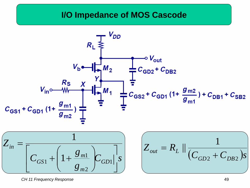
I/O Impedance of MOS Cascode
sCggC
Z
GDm
mGS
in
++
=
12
11 1
1
( )sCCRZ
DBGDLout
22
1||+
=
CH 11 Frequency Response 50
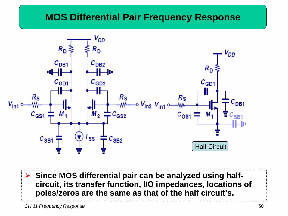
MOS Differential Pair Frequency Response
Since MOS differential pair can be analyzed using half-circuit, its transfer function, I/O impedances, locations of poles/zeros are the same as that of the half circuit’s.
Half Circuit
CH 11 Frequency Response 51
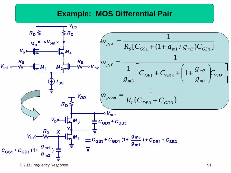
Example: MOS Differential Pair
( )33,
11
331
3
,
1311,
1
111
])/1([1
GDDBLoutp
GDm
mGSDB
m
Yp
GDmmGSSXp
CCR
CggCC
g
CggCR
+=
+++
=
++=
ω
ω
ω
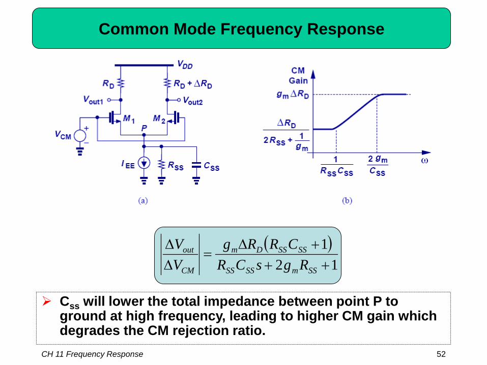
Common Mode Frequency Response
( )12
1++
+∆=
∆∆
SSmSSSS
SSSSDm
CM
out
RgsCRCRRg
VV
Css will lower the total impedance between point P to ground at high frequency, leading to higher CM gain which degrades the CM rejection ratio.
CH 11 Frequency Response 52
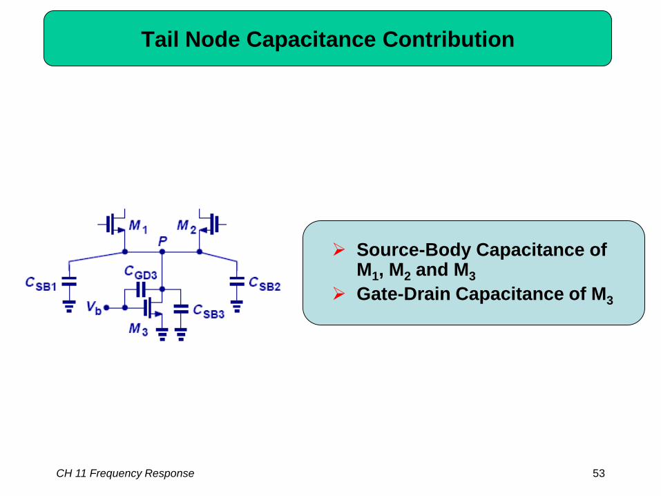
Tail Node Capacitance Contribution
Source-Body Capacitance of M1, M2 and M3
Gate-Drain Capacitance of M3
CH 11 Frequency Response 53

54
Chapter 12 Feedback
Microelectronics, 2nd edition by Behzad Razavi
CH 12 Feedback 55
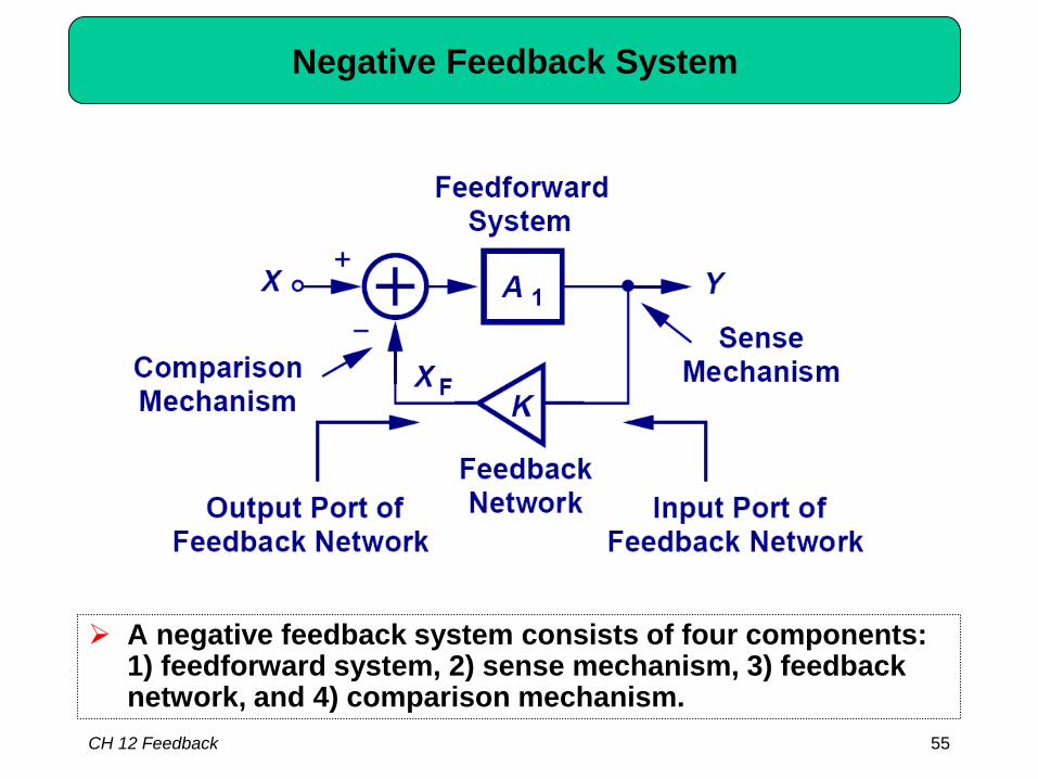
Negative Feedback System
A negative feedback system consists of four components: 1) feedforward system, 2) sense mechanism, 3) feedback network, and 4) comparison mechanism.
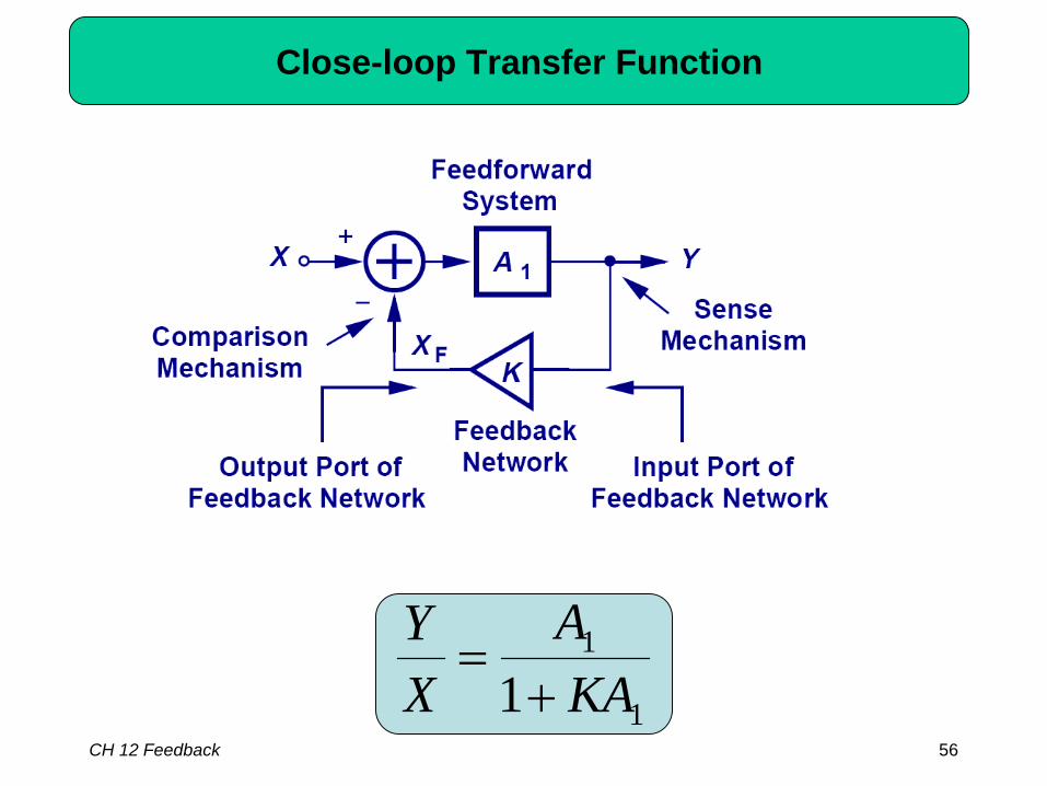
CH 12 Feedback 56
Close-loop Transfer Function
1
1
1 KAA
XY
+=
CH 12 Feedback 57
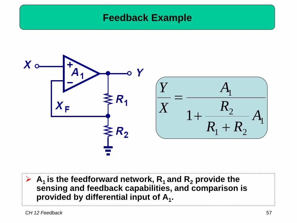
Feedback Example
A1 is the feedforward network, R1 and R2 provide the sensing and feedback capabilities, and comparison is provided by differential input of A1.
121
2
1
1 ARR
RA
XY
++
=
CH 12 Feedback 58
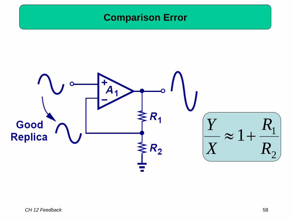
Comparison Error
2
11RR
XY
+≈
CH 12 Feedback 59
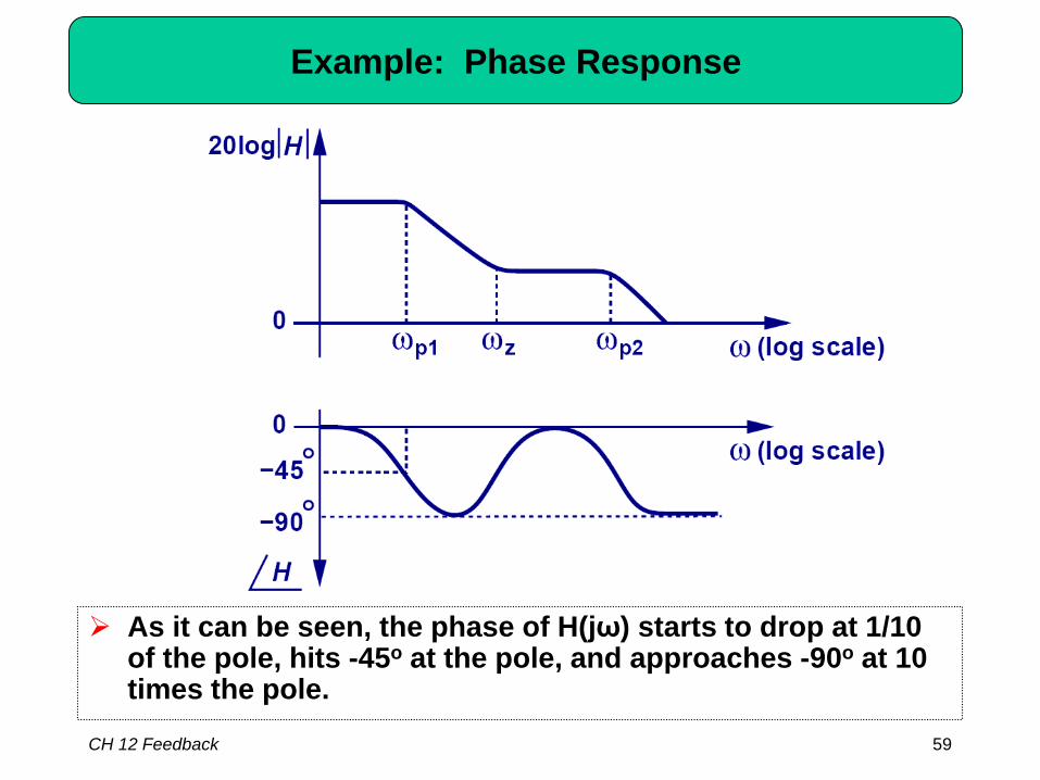
Example: Phase Response
As it can be seen, the phase of H(jω) starts to drop at 1/10 of the pole, hits -45o at the pole, and approaches -90o at 10 times the pole.
CH 12 Feedback 60
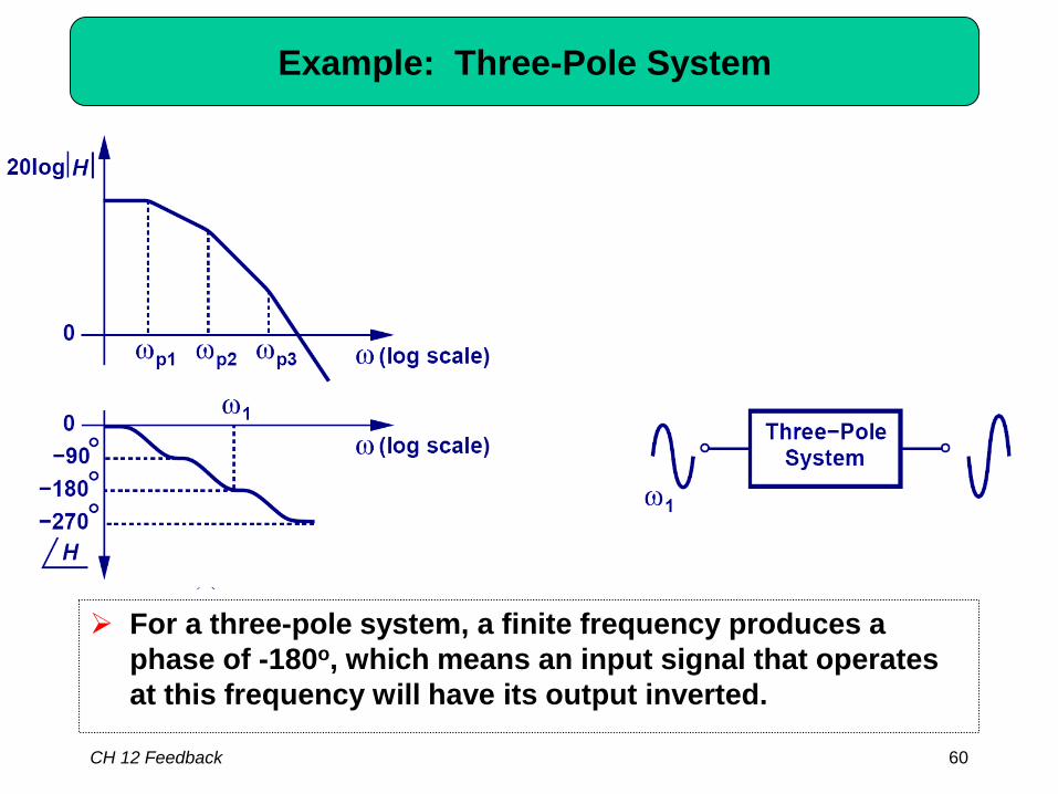
Example: Three-Pole System
For a three-pole system, a finite frequency produces a phase of -180o, which means an input signal that operates at this frequency will have its output inverted.
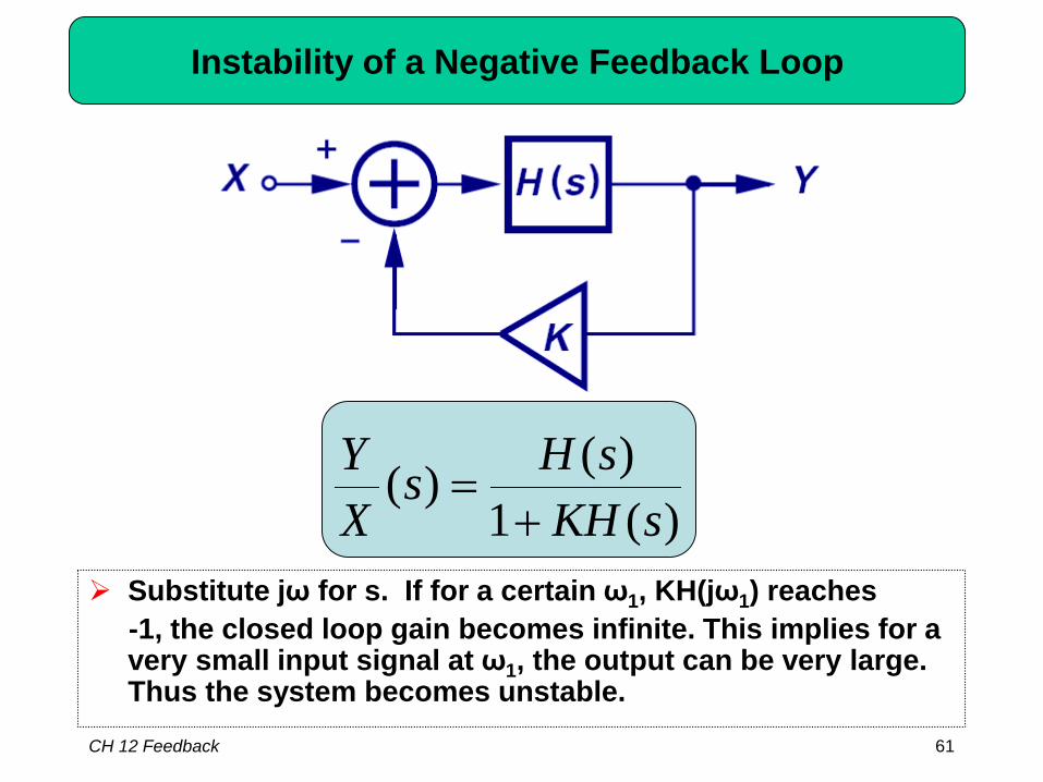
CH 12 Feedback 61
Instability of a Negative Feedback Loop
Substitute jω for s. If for a certain ω1, KH(jω1) reaches -1, the closed loop gain becomes infinite. This implies for a very small input signal at ω1, the output can be very large. Thus the system becomes unstable.
)(1)()(
sKHsHs
XY
+=
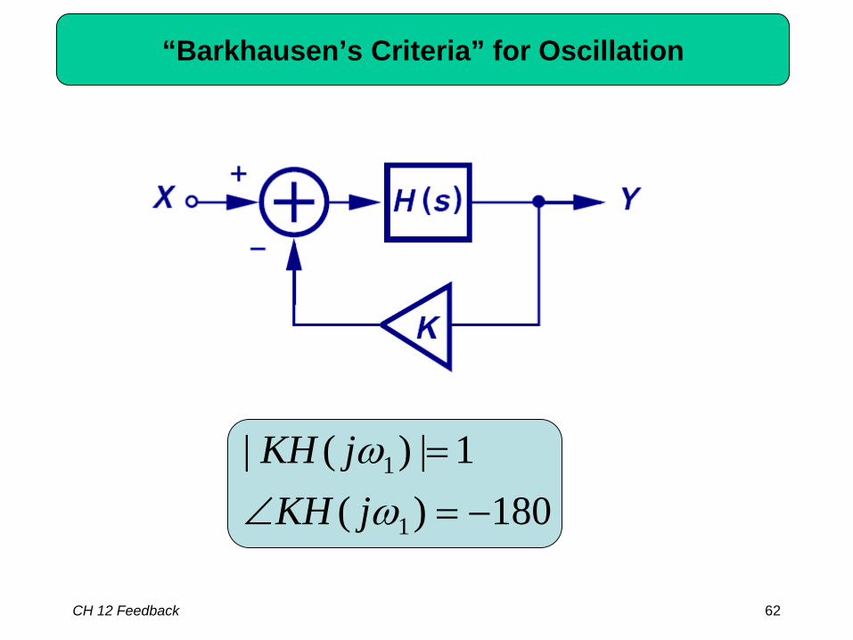
CH 12 Feedback 62
“Barkhausen’s Criteria” for Oscillation
180)(1|)(|
1
1
−=∠=
ωωjKH
jKH
CH 12 Feedback 63
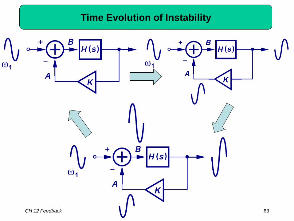
Time Evolution of Instability
CH 12 Feedback 64
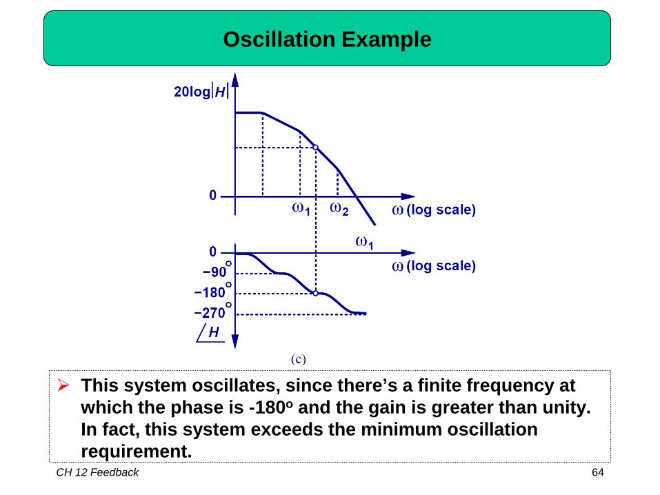
Oscillation Example
This system oscillates, since there’s a finite frequency at which the phase is -180o and the gain is greater than unity. In fact, this system exceeds the minimum oscillation requirement.
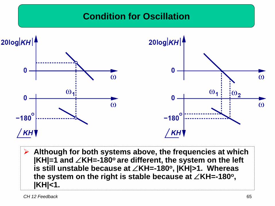
CH 12 Feedback 65
Condition for Oscillation
Although for both systems above, the frequencies at which |KH|=1 and ∠KH=-180o are different, the system on the left is still unstable because at ∠KH=-180o, |KH|>1. Whereas the system on the right is stable because at ∠KH=-180o, |KH|<1.
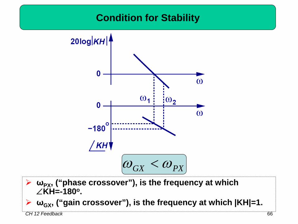
CH 12 Feedback 66
Condition for Stability
ωPX, (“phase crossover”), is the frequency at which ∠KH=-180o.
ωGX, (“gain crossover”), is the frequency at which |KH|=1.
PXGX ωω <
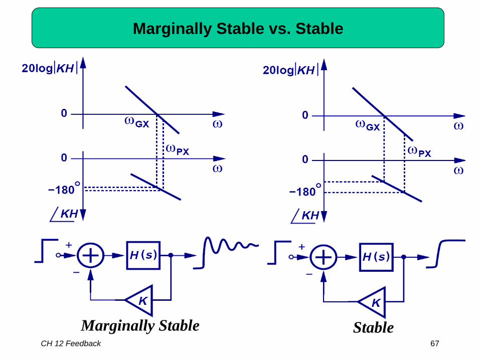
CH 12 Feedback 67
Marginally Stable vs. Stable
Marginally Stable Stable
CH 12 Feedback 68
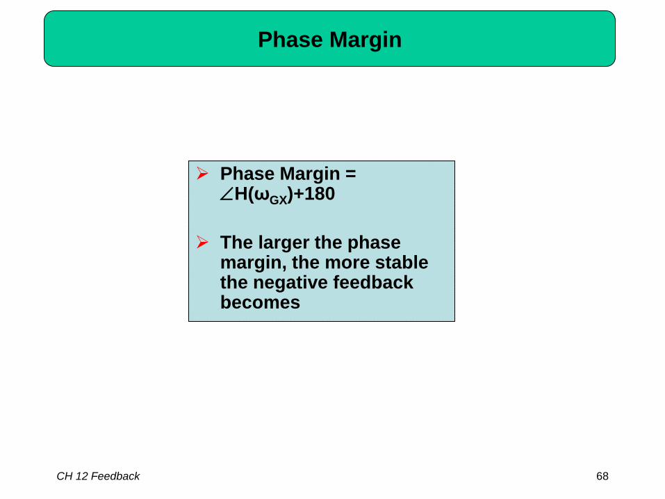
Phase Margin
Phase Margin = ∠H(ωGX)+180
The larger the phase margin, the more stable the negative feedback becomes
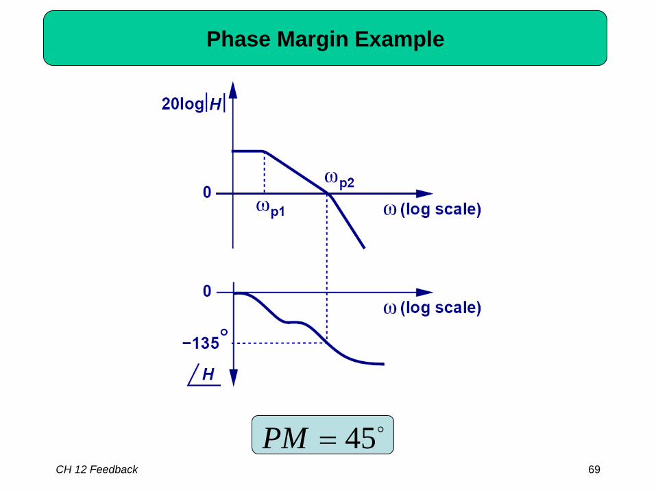
CH 12 Feedback 69
Phase Margin Example
45=PM
CH 12 Feedback 70
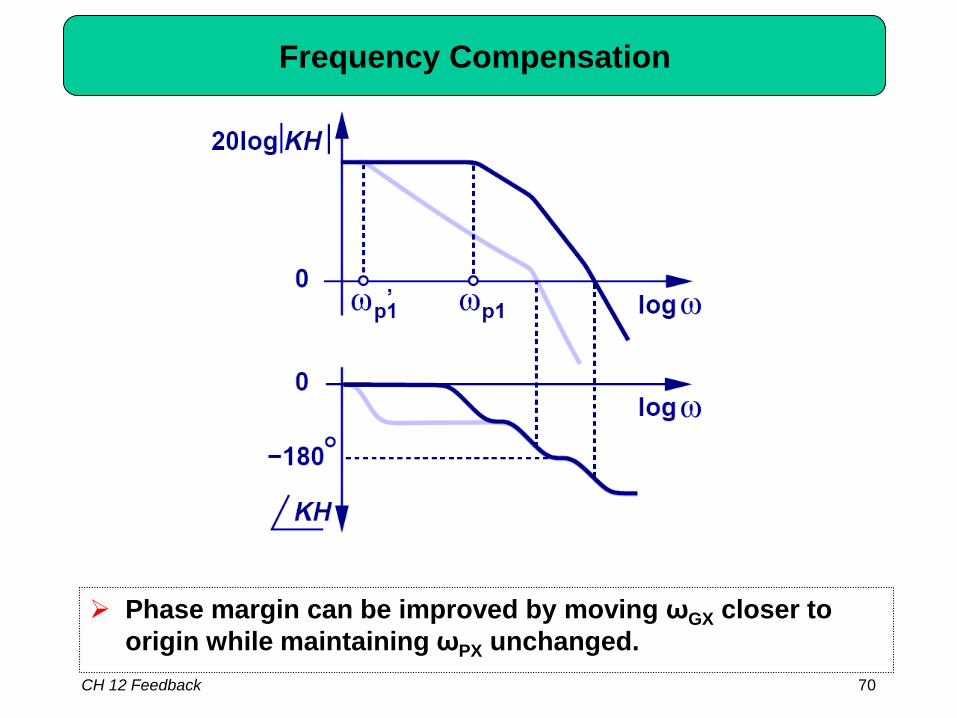
Frequency Compensation
Phase margin can be improved by moving ωGX closer to origin while maintaining ωPX unchanged.
CH 12 Feedback 71
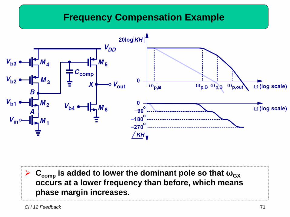
Frequency Compensation Example
Ccomp is added to lower the dominant pole so that ωGX occurs at a lower frequency than before, which means phase margin increases.
CH 12 Feedback 72
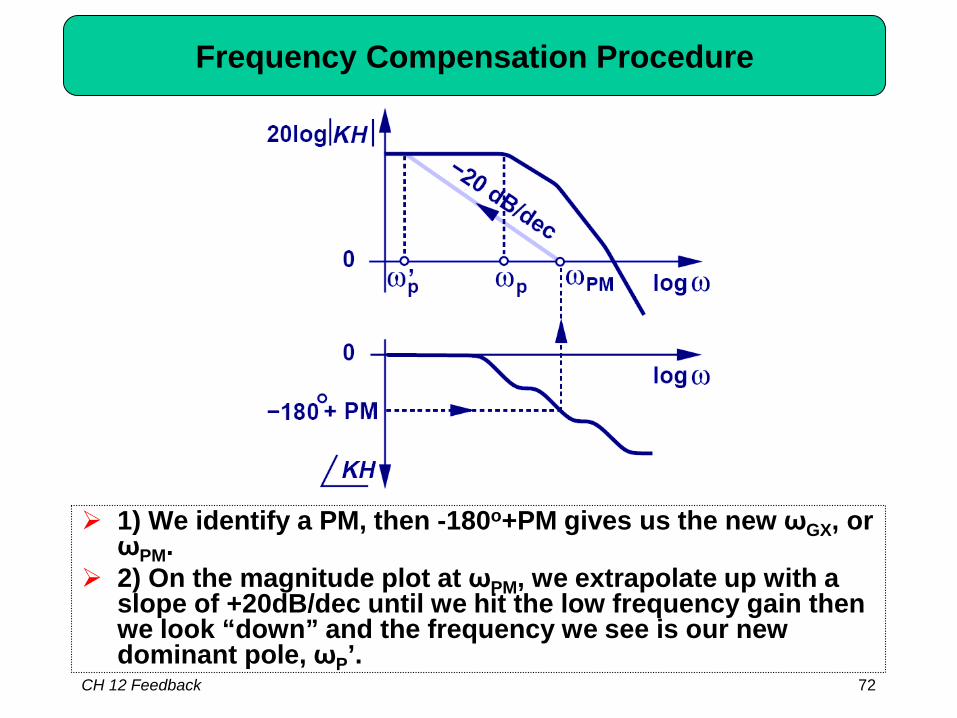
Frequency Compensation Procedure
1) We identify a PM, then -180o+PM gives us the new ωGX, or ωPM.
2) On the magnitude plot at ωPM, we extrapolate up with a slope of +20dB/dec until we hit the low frequency gain then we look “down” and the frequency we see is our new dominant pole, ωP’.
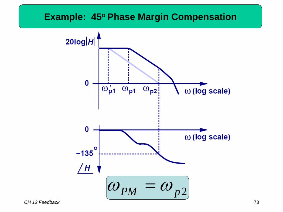
CH 12 Feedback 73
Example: 45o Phase Margin Compensation
2pPM ωω =
CH 12 Feedback 74
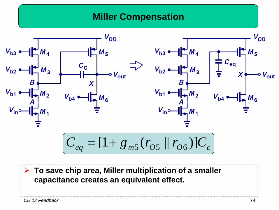
Miller Compensation
To save chip area, Miller multiplication of a smaller capacitance creates an equivalent effect.
cOOmeq CrrgC )]||(1[ 655+=
![Cascode Switching Modeling and Improvement in Flyback ...Cascode GaN FET [10], during inductive hard switching. Figure 2 Cascode Switching Configured Flyback converter II. MODELING](https://img.pdfslide.net/doc/110x75/5e541119f61a9f6e2b2e813c/cascode-switching-modeling-and-improvement-in-flyback-cascode-gan-fet-10.jpg)