Embed Size (px)
Citation preview
Chapter 9 – Switched Capacitor Circuits 5/2/04
CMOS Analog Circuit Design © P.E. Allen - 2004
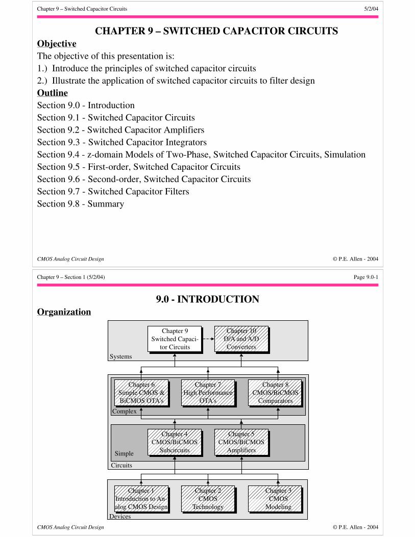
CHAPTER 9 – SWITCHED CAPACITOR CIRCUITSObjectiveThe objective of this presentation is:1.) Introduce the principles of switched capacitor circuits2.) Illustrate the application of switched capacitor circuits to filter designOutlineSection 9.0 - IntroductionSection 9.1 - Switched Capacitor CircuitsSection 9.2 - Switched Capacitor AmplifiersSection 9.3 - Switched Capacitor IntegratorsSection 9.4 - z-domain Models of Two-Phase, Switched Capacitor Circuits, SimulationSection 9.5 - First-order, Switched Capacitor CircuitsSection 9.6 - Second-order, Switched Capacitor CircuitsSection 9.7 - Switched Capacitor FiltersSection 9.8 - Summary
Chapter 9 – Section 1 (5/2/04) Page 9.0-1
CMOS Analog Circuit Design © P.E. Allen - 2004
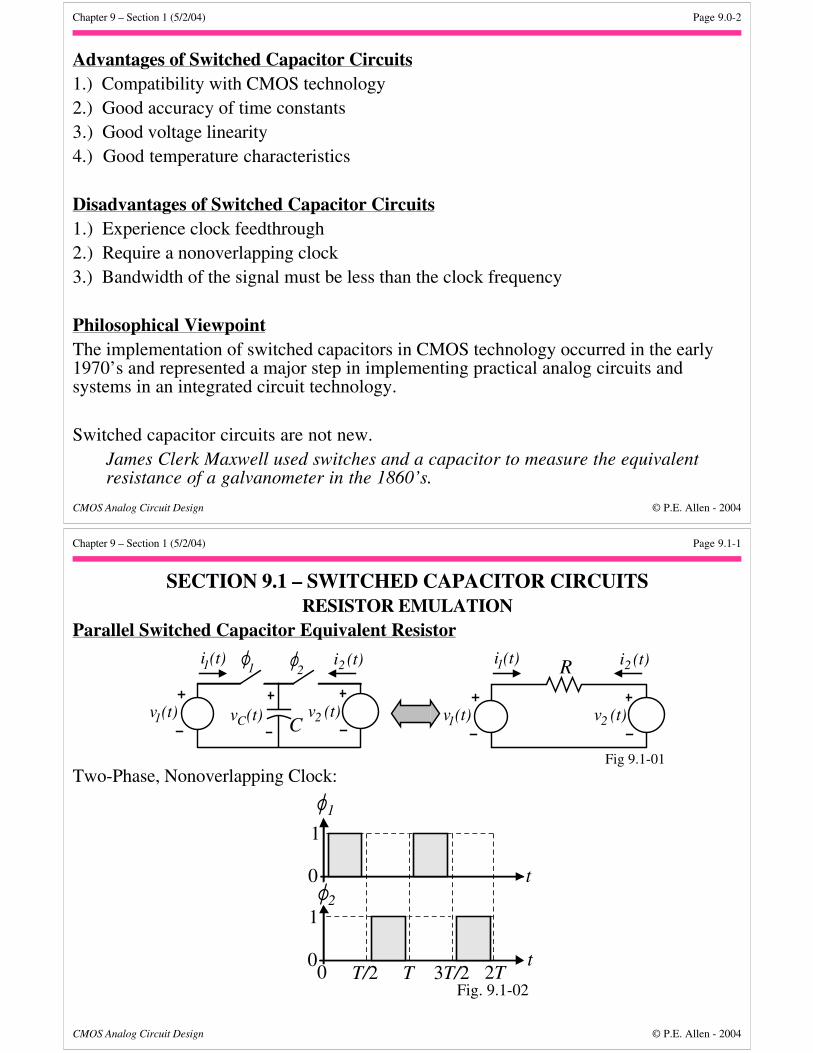
9.0 - INTRODUCTIONOrganization
Chapter 9
Switched Capaci-tor Circuits
Chapter 6Simple CMOS &BiCMOS OTA's
Chapter 7High Performance
OTA's
Chapter 10D/
Chapter 11AnalogSystems
Chapter 3
CMOSModeling
Chapter 4
CMOS/BiCMOSSubcircuits
Chapter 5CMOS/BiCMOS
Amplifiers
Systems
Complex
Circuits
Devices
Simple
Chapter 2CMOS
Technology
Chapter 1Introduction to An-alog CMOS Design
Chapter 8CMOS/BiCMOS
Comparators
Chapter 10D/A and A/DConverters
Chapter 9 – Section 1 (5/2/04) Page 9.0-2
CMOS Analog Circuit Design © P.E. Allen - 2004
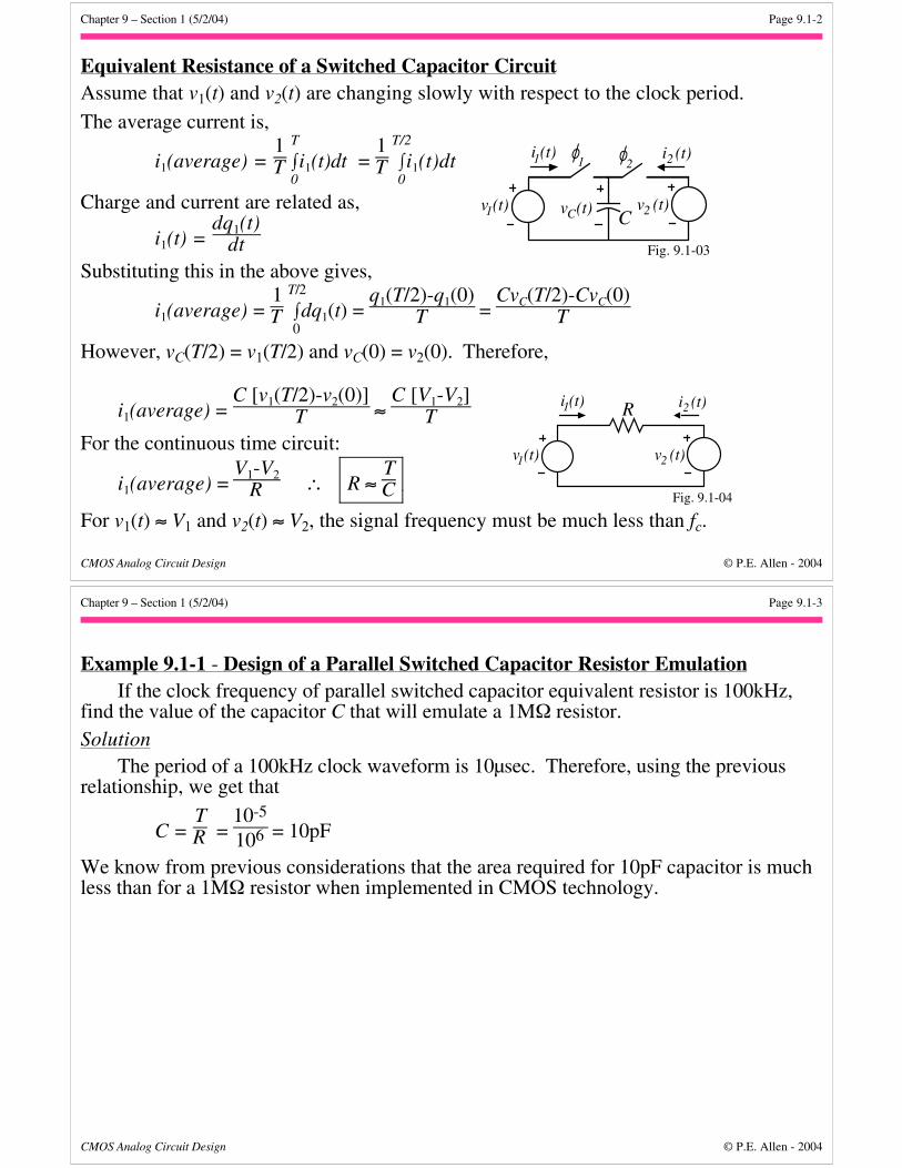
Advantages of Switched Capacitor Circuits1.) Compatibility with CMOS technology2.) Good accuracy of time constants3.) Good voltage linearity4.) Good temperature characteristics
Disadvantages of Switched Capacitor Circuits1.) Experience clock feedthrough2.) Require a nonoverlapping clock3.) Bandwidth of the signal must be less than the clock frequency
Philosophical ViewpointThe implementation of switched capacitors in CMOS technology occurred in the early1970’s and represented a major step in implementing practical analog circuits andsystems in an integrated circuit technology.
Switched capacitor circuits are not new.James Clerk Maxwell used switches and a capacitor to measure the equivalentresistance of a galvanometer in the 1860’s.
Chapter 9 – Section 1 (5/2/04) Page 9.1-1
CMOS Analog Circuit Design © P.E. Allen - 2004
SECTION 9.1 – SWITCHED CAPACITOR CIRCUITSRESISTOR EMULATION
Parallel Switched Capacitor Equivalent Resistor
i (t) i (t)2
v (t)1 v (t)2
1 Ri (t) i (t)2
Cv (t)1 v (t)2
1 1 2
v (t)C
Fig 9.1-01Two-Phase, Nonoverlapping Clock:
t
t
1
0
1
00 T/2 T 3T/2 2T
2
1
Fig. 9.1-02
Chapter 9 – Section 1 (5/2/04) Page 9.1-2
CMOS Analog Circuit Design © P.E. Allen - 2004
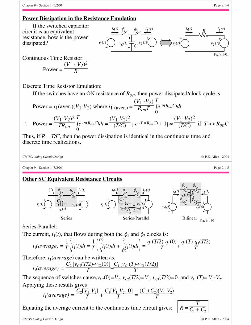
Equivalent Resistance of a Switched Capacitor CircuitAssume that v1(t) and v2(t) are changing slowly with respect to the clock period.
The average current is,
i1(average) = 1T ⌡⌠
0
T
i1(t)dt = 1T ⌡⌠
0
T/2
i1(t)dt
Charge and current are related as,
i1(t) = dq1(t)
dtSubstituting this in the above gives,
i1(average) = 1T ⌡⌠
0
T/2
dq1(t) = q1(T/2)-q1(0)
T = CvC(T/2)-CvC(0)
T
However, vC(T/2) = v1(T/2) and vC(0) = v2(0). Therefore,
i1(average) = C [v1(T/2)-v2(0)]
T ≈ C [V1-V2]
T
For the continuous time circuit:
i1(average) = V1-V2
R ∴ R ≈ TC
For v1(t) ≈ V1 and v2(t) ≈ V2, the signal frequency must be much less than fc.
i (t) i (t)2
Cv (t)1 v (t)2
1 1 2
v (t)C
Fig. 9.1-03
i (t) i (t)2
v (t)1 v (t)2
1 R
Fig. 9.1-04
Chapter 9 – Section 1 (5/2/04) Page 9.1-3
CMOS Analog Circuit Design © P.E. Allen - 2004
Example 9.1-1 - Design of a Parallel Switched Capacitor Resistor EmulationIf the clock frequency of parallel switched capacitor equivalent resistor is 100kHz,
find the value of the capacitor C that will emulate a 1MΩ resistor.Solution
The period of a 100kHz clock waveform is 10µsec. Therefore, using the previousrelationship, we get that
C = TR =
10-5
106 = 10pF
We know from previous considerations that the area required for 10pF capacitor is muchless than for a 1MΩ resistor when implemented in CMOS technology.
Chapter 9 – Section 1 (5/2/04) Page 9.1-4
CMOS Analog Circuit Design © P.E. Allen - 2004
Power Dissipation in the Resistance EmulationIf the switched capacitor
circuit is an equivalentresistance, how is the powerdissipated?
Continuous Time Resistor:
Power = (V1 - V2)2
R
Discrete Time Resistor Emulation:If the switches have an ON resistance of Ron, then power dissipated/clock cycle is,
Power = i1(aver.)(V1-V2) where i1 (aver.) = (V1 -V2)
RonT ⌡⌠0
Te-t/(RonC)dt
∴ Power = (V1-V2)2
TRon ⌡⌠0
Te -t/(RonC)dt =
(V1-V2)2
(T/C) -e -T /(RonC) + 1 ≈ (V1-V2)2
(T/C) if T >> RonC
Thus, if R = T/C, then the power dissipation is identical in the continuous time anddiscrete time realizations.
i (t) i (t)2
v (t)1 v (t)2
1 Ri (t) i (t)2
Cv (t)1 v (t)2
1 1 2
v (t)C
Fig 9.1-01
Chapter 9 – Section 1 (5/2/04) Page 9.1-5
CMOS Analog Circuit Design © P.E. Allen - 2004
Other SC Equivalent Resistance Circuits
Series
i (t)2
v (t)1 v (t)2
i (t)1 1 2
1S 2SC
v (t)C
Series-Parallel
i (t)2
Cv (t)1 v (t)2
i (t)1 1 2
1S 2S1
C2
v (t)C1 v (t)C2 1
1S i (t)2
v (t) v (t)2
i (t)1
1 2
2SC
121S 2S
Bilinear
v (t)C
Fig. 9.1-05
Series-Parallel:The current, i1(t), that flows during both the φ1 and φ2 clocks is:
i1(average) = 1T ⌡⌠
0
T
i1(t)dt = 1T
⌡⌠
0
T/2
i1(t)dt + ⌡⌠
T/2
T
i1(t)dt = q1(T/2)-q1(0)
T + q1(T)-q1(T/2)
T
Therefore, i1(average) can be written as,
i1(average) = C2 [vC2(T/2)-vC2(0)]
T +C1 [vC1(T)-vC1(T/2)]
T
The sequence of switches cause,vC2(0)=V2, vC2(T/2)=V1, vC1(T/2)=0, and vC1(T)= V1-V2.Applying these results gives
i1(average) = C2[V1-V2]
T + C1[V1-V2- 0]
T = (C1+C2)(V1-V2)
T
Equating the average current to the continuous time circuit gives: R = T
C1 + C2
Chapter 9 – Section 1 (5/2/04) Page 9.1-6
CMOS Analog Circuit Design © P.E. Allen - 2004
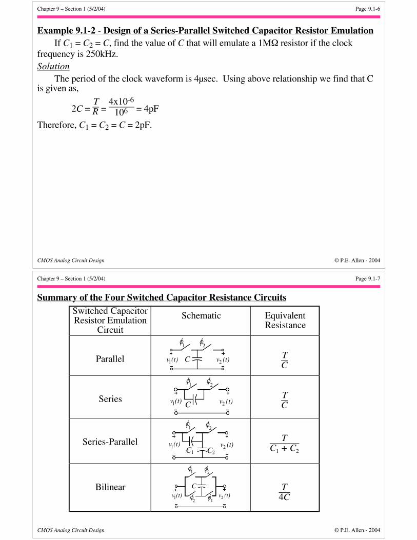
Example 9.1-2 - Design of a Series-Parallel Switched Capacitor Resistor EmulationIf C1 = C2 = C, find the value of C that will emulate a 1MΩ resistor if the clock
frequency is 250kHz.Solution
The period of the clock waveform is 4µsec. Using above relationship we find that Cis given as,
2C = TR =
4x10⁻⁶
106 = 4pF
Therefore, C1 = C2 = C = 2pF.
Chapter 9 – Section 1 (5/2/04) Page 9.1-7
CMOS Analog Circuit Design © P.E. Allen - 2004
Summary of the Four Switched Capacitor Resistance CircuitsSwitched CapacitorResistor Emulation
Circuit
Schematic EquivalentResistance
Parallel Cv (t)1 v (t)2
1 2
TC
Series v (t)1 v (t)2
1 2
CTC
Series-ParallelC
v (t)1 v (t)2
1 2
1 C2
TC1 + C2
Bilinear1v (t) v (t)2
1 2
C
2 1
T4C
Chapter 9 – Section 1 (5/2/04) Page 9.1-8
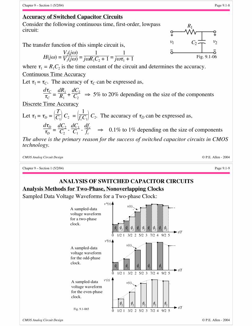
CMOS Analog Circuit Design © P.E. Allen - 2004
Accuracy of Switched Capacitor CircuitsConsider the following continuous time, first-order, lowpasscircuit:
The transfer function of this simple circuit is,
H(jω) = V2(jω)V1(jω) =
1jωR1C2 + 1 =
1jωτ1 + 1
where τ1 = R1C2 is the time constant of the circuit and determines the accuracy.Continuous Time AccuracyLet τ1 = τC. The accuracy of τC can be expressed as,
dτC
τC =
dR1
R1 +
dC2
C2 ⇒ 5% to 20% depending on the size of the components
Discrete Time Accuracy
Let τ1 = τD =
T
C1 C2 =
1
fcC1 C2. The accuracy of τD can be expressed as,
dτD
τD =
dC2
C2 -
dC1
C1 -
dfc
fc ⇒ 0.1% to 1% depending on the size of components
The above is the primary reason for the success of switched capacitor circuits in CMOStechnology.
R1
C21v v2
Fig. 9.1-06
Chapter 9 – Section 1 (5/2/04) Page 9.1-9
CMOS Analog Circuit Design © P.E. Allen - 2004
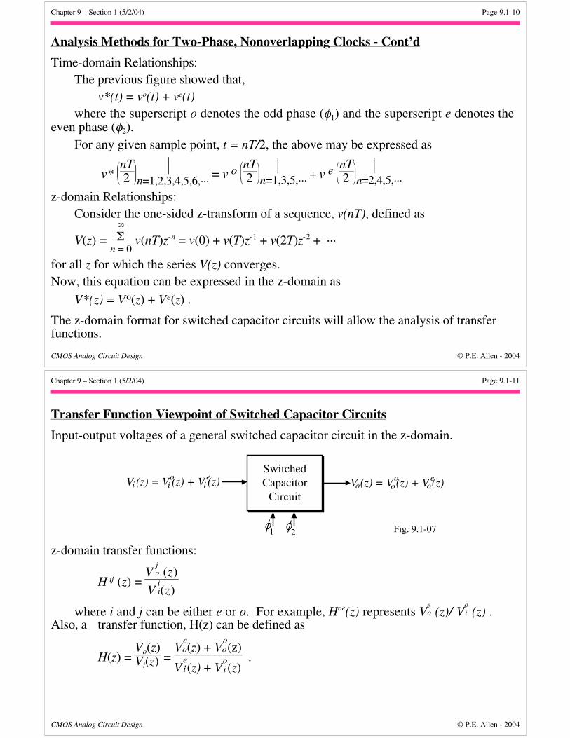
ANALYSIS OF SWITCHED CAPACITOR CIRCUITSAnalysis Methods for Two-Phase, Nonoverlapping ClocksSampled Data Voltage Waveforms for a Two-phase Clock:
0 1/2 1 3/2 2 5/2 3 7/2 4 9/2 5t/T
v(t)v*(t)
1 2 2 2 2 21 1 1 1
v (t)O
v (t)e
0 1/2 1 3/2 2 5/2 3 7/2 4 9/2 5t/T
v(t)
1 1 1 1 1
0 1/2 1 3/2 2 5/2 3 7/2 4 9/2 5t/T
v(t)
2 2 2 2 2
A sampled-datavoltage waveformfor a two-phaseclock.
A sampled-datavoltage waveformfor the odd-phaseclock.
A sampled-datavoltage waveformfor the even-phaseclock.
Fig. 9.1-065
Chapter 9 – Section 1 (5/2/04) Page 9.1-10
CMOS Analog Circuit Design © P.E. Allen - 2004
Analysis Methods for Two-Phase, Nonoverlapping Clocks - Cont’d
Time-domain Relationships:The previous figure showed that,
v*(t) = vo(t) + ve(t) where the superscript o denotes the odd phase (φ1) and the superscript e denotes the
even phase (φ2).For any given sample point, t = nT/2, the above may be expressed as
v*
nT
2
n=1,2,3,4,5,6,··· = v o
nT
2
n=1,3,5,··· + v e
nT
2
n=2,4,5,···
z-domain Relationships:Consider the one-sided z-transform of a sequence, v(nT), defined as
V(z) = ∞Σ
n = 0 v(nT)z- n = v(0) + v(T)z- 1 + v(2T)z- 2 + ···
for all z for which the series V(z) converges.Now, this equation can be expressed in the z-domain as
V*(z) = Vo(z) + Ve(z) .
The z-domain format for switched capacitor circuits will allow the analysis of transferfunctions.
Chapter 9 – Section 1 (5/2/04) Page 9.1-11
CMOS Analog Circuit Design © P.E. Allen - 2004
Transfer Function Viewpoint of Switched Capacitor Circuits
Input-output voltages of a general switched capacitor circuit in the z-domain.
SwitchedCapacitor
Circuit
1 2
V (z) = V (z) + V (z)io e
i i V (z) = V (z) + V (z)oo e
o o
Fig. 9.1-07
z-domain transfer functions:
H ij (z) = V
j o (z)
Vi i(z)
where i and j can be either e or o. For example, Hoe(z) represents Veo (z)/ V
oi (z) .
Also, a transfer function, H(z) can be defined as
H(z) = Vo(z)Vi(z) =
Veo(z) + V
oo(z)
Vei(z) + V
oi (z)
.

Chapter 9 – Section 1 (5/2/04) Page 9.1-12
CMOS Analog Circuit Design © P.E. Allen - 2004
Approach for Analyzing Switched Capacitor Circuits1.) Analyze the circuit in the time-domain during a selected phase period.2.) The resulting equations are based on q = Cv.3.) Analyze the following phase period carrying over the initial conditions from the
previous analysis.4.) Identify the time-domain equation that relates the desired voltage variables.5.) Convert this equation to the z-domain.6.) Solve for the desired z-domain transfer function.
7.) Replace z by ejωT and examine the frequency response.
Chapter 9 – Section 1 (5/2/04) Page 9.1-13
CMOS Analog Circuit Design © P.E. Allen - 2004
Example 9.1-3 - Analysis of a Switched Capacitor, First-order, Low pass FilterUse the above approach to find the z-domain transfer function of the first-order, low
pass switched capacitor circuit shown below. This circuit was developed by replacingthe resistor, R1, of the previous circuit with the parallel switched capacitor resistor circuit.The timing of the clocks is also shown. This timing is arbitrary and is used to assist theanalysis and does not change the result.
Switched capacitor, low pass filter.
2Cv 1 v 21
1 2
C
Clock phasing for this example.
tTn-1n-3
2 n-12 n+ 1
2n
1 12 2 2
n+1
Fig. 9.1-08
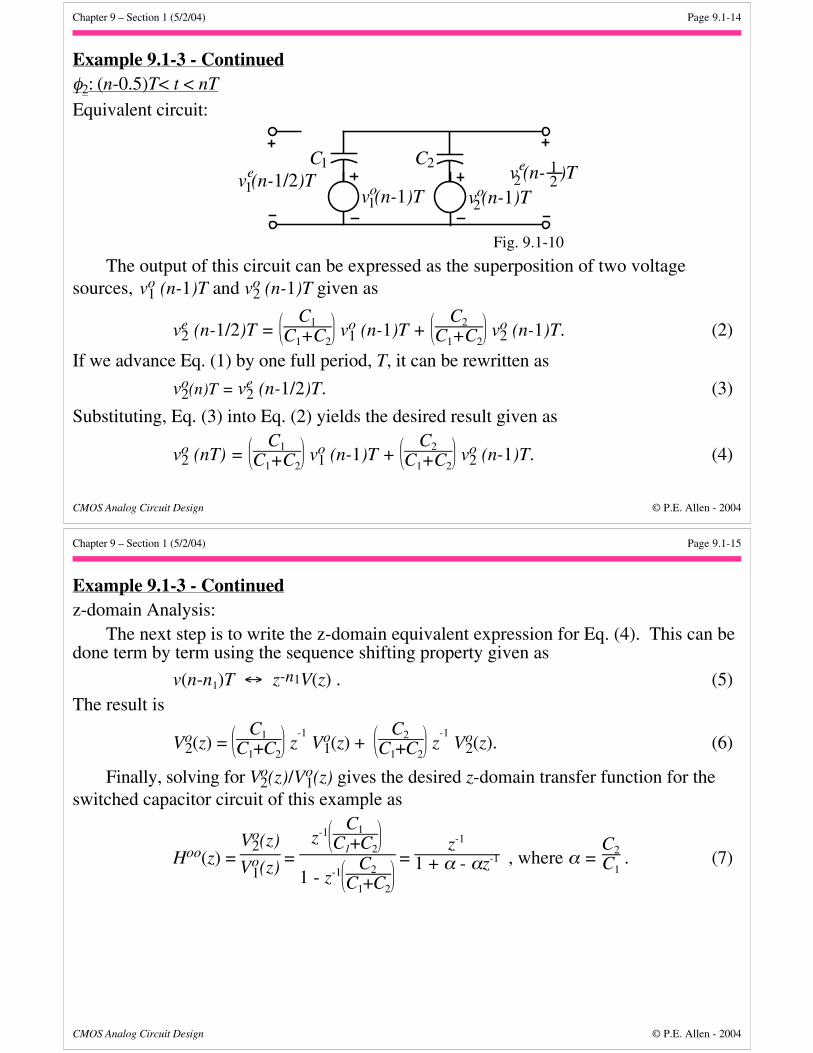
Solutionφ1: (n-1)T< t < (n-0.5)T
Equivalent circuit:
C2C1v (n-1)T1o v (n- )T3
2e2 v (n-1)To
2
Equivalent circuit.
C1
C2
v (n-1)T1o v (n- )T3
2e2 v (n-1)To
2
Simplified equivalent circuit.Fig. 9.1-09
The voltage at the output (across C2) is vo2(n-1)T = ve
2 (n-3/2)T (1)
Chapter 9 – Section 1 (5/2/04) Page 9.1-14
CMOS Analog Circuit Design © P.E. Allen - 2004
Example 9.1-3 - Continuedφ2: (n-0.5)T< t < nT
Equivalent circuit:
C1
C2v (n-1/2)T1
e v (n- )T12
e2
v (n-1)To2v (n-1)To
1
C1
Fig. 9.1-10
The output of this circuit can be expressed as the superposition of two voltagesources, vo
1 (n-1)T and vo2 (n-1)T given as
ve2 (n-1/2)T =
C1
C1+C2 vo
1 (n-1)T +
C2
C1+C2 vo
2 (n-1)T. (2)
If we advance Eq. (1) by one full period, T, it can be rewritten as
vo2(n)T = ve
2 (n-1/2)T. (3)
Substituting, Eq. (3) into Eq. (2) yields the desired result given as
vo2 (nT) =
C1
C1+C2 vo
1 (n-1)T +
C2
C1+C2 vo
2 (n-1)T. (4)
Chapter 9 – Section 1 (5/2/04) Page 9.1-15
CMOS Analog Circuit Design © P.E. Allen - 2004
Example 9.1-3 - Continuedz-domain Analysis:
The next step is to write the z-domain equivalent expression for Eq. (4). This can bedone term by term using the sequence shifting property given as
v(n-n1)T ↔ z-n1V(z) . (5)The result is
Vo2(z) =
C1
C1+C2 z
-1 Vo
1(z) +
C2
C1+C2 z
-1 Vo
2(z). (6)
Finally, solving for Vo2(z)/Vo
1(z) gives the desired z-domain transfer function for theswitched capacitor circuit of this example as
Hoo(z) = Vo
2(z)
Vo1(z) =
z-1
C1
C1+C2
1 - z-1
C2
C1+C2
= z-1
1 + α - αz-1 , where α = C2
C1 . (7)

Chapter 9 – Section 1 (5/2/04) Page 9.1-16
CMOS Analog Circuit Design © P.E. Allen - 2004
Discrete-Frequency Domain AnalysisRelationship between the continuous and discrete frequency domains:
z = e jωT
Illustration:j
= ∞
= 0
= -∞
Continuoustime frequency
response
Continuous Frequency Domain
Imaginary Axis
RealAxis
+j1
-j1
+1-1
r = 1
Discretetime frequency
response
= -∞
= ∞ = 0
Discrete Frequency DomainFig. 9.1-11
Chapter 9 – Section 1 (5/2/04) Page 9.1-17
CMOS Analog Circuit Design © P.E. Allen - 2004
Example 9.1-4 - Frequency Response of Example 9.1-3Use the results of the previous example to find the magnitude and phase of the
discrete time frequency response for the switched capacitor circuit of Example 3.Solution
The first step is to replace z in Hoo(z) of Ex. 3 by e jωT. The result is given below as
Hoo ejωΤ =
e-jωT
1+α-α e-jωT = 1
(1+α)ejωT- α = 1
(1+α)cos(ωT)- α + j(1+α)sin(ωT) (1)
where we have used Eulers formula to replace e jωT by cos(ωT)+jsin(ωT). The magnitudeof Eq. (1) is found by taking the square root of the square of the real and imaginarycomponents of the denominator to give
Hoo = 1
(1+α)2cos2(ωT) - 2α(1+α)cos(ωT) + α2 + (1+α)2sin2(ωT)
= 1
(1+α)2[cos2(ωT)+sin2(ωT)]+α2-2α(1+α)cos(ωT)
= 1
1+2α+α2 -2α(1+α)cos(ωT) = 1
1+2α(1+α)(1-cos(ωT)) . (2)
The phase shift of Eq. (1) is expressed as
Arg Hoo = - tan-1
(1+α)sin(ωT)
(1+α)cos(ωT)-α = - tan-1
sin(ωT)
cos(ωT) - α
1+α(3)
Chapter 9 – Section 1 (5/2/04) Page 9.1-18
CMOS Analog Circuit Design © P.E. Allen - 2004
The Oversampling AssumptionThe oversampling assumption is simply to assume that fsignal << fclock = fc.
This means that,
fsignal = f << 1T ⇒ 2πf = ω <<
2πT ⇒ ωT << 2π.
The importance of the oversampling assumption is that is permits the design of switchedcapacitor circuits that approximates the continuous time circuit until the signal frequencybegins to approach the clock frequency.
Chapter 9 – Section 1 (5/2/04) Page 9.1-19
CMOS Analog Circuit Design © P.E. Allen - 2004
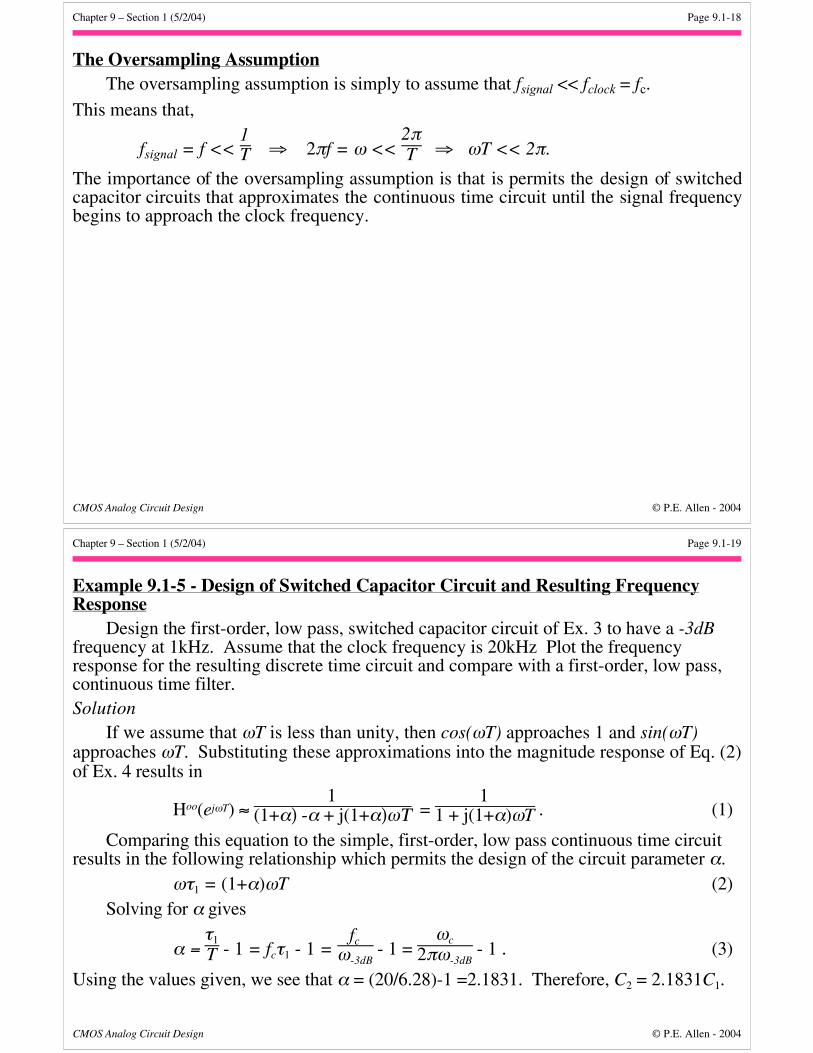
Example 9.1-5 - Design of Switched Capacitor Circuit and Resulting FrequencyResponse
Design the first-order, low pass, switched capacitor circuit of Ex. 3 to have a -3dBfrequency at 1kHz. Assume that the clock frequency is 20kHz Plot the frequencyresponse for the resulting discrete time circuit and compare with a first-order, low pass,continuous time filter.Solution
If we assume that ωT is less than unity, then cos(ωT) approaches 1 and sin(ωT)approaches ωT. Substituting these approximations into the magnitude response of Eq. (2)of Ex. 4 results in
Hoo(ejωT) ≈ 1
(1+α) -α + j(1+α)ωΤ = 1
1 + j(1+α)ωT . (1)
Comparing this equation to the simple, first-order, low pass continuous time circuitresults in the following relationship which permits the design of the circuit parameter α.
ωτ1 = (1+α)ωT (2)Solving for α gives
α = τ1
T - 1 = fcτ1 - 1 = fc
ω-3dB - 1 =
ωc
2πω-3dB - 1 . (3)
Using the values given, we see that α = (20/6.28)-1 =2.1831. Therefore, C2 = 2.1831C1.
Chapter 9 – Section 1 (5/2/04) Page 9.1-20
CMOS Analog Circuit Design © P.E. Allen - 2004
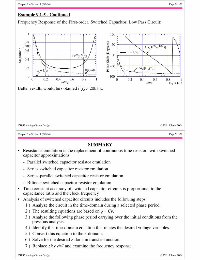
Example 9.1-5 - Continued
Frequency Response of the First-order, Switched Capacitor, Low Pass Circuit:
0
0.2
0.4
0.6
0.8
1
0 0.2 0.4 0.6 0.8 1
Mag
nitu
de
0.707
|H(jω)|
|Hoo(ejωT)|
ω = 1/τ1
ω/ωc
-100
-50
0
50
100
0 0.2 0.4 0.6 0.8 1
Phas
e Sh
ift (
Deg
rees
)
ω/ωc
Arg[Hoo(ejωT)]
Arg[H(jω)]
ω = 1/τ1
Fig. 9.1-12
Better results would be obtained if fc > 20kHz.
Chapter 9 – Section 1 (5/2/04) Page 9.1-21
CMOS Analog Circuit Design © P.E. Allen - 2004
SUMMARY• Resistance emulation is the replacement of continuous time resistors with switched
capacitor approximations
- Parallel switched capacitor resistor emulation
- Series switched capacitor resistor emulation
- Series-parallel switched capacitor resistor emulation
- Bilinear switched capacitor resistor emulation• Time constant accuracy of switched capacitor circuits is proportional to the
capacitance ratio and the clock frequency• Analysis of switched capacitor circuits includes the following steps:
1.) Analyze the circuit in the time-domain during a selected phase period.2.) The resulting equations are based on q = Cv.3.) Analyze the following phase period carrying over the initial conditions from the
previous analysis.4.) Identify the time-domain equation that relates the desired voltage variables.5.) Convert this equation to the z-domain.6.) Solve for the desired z-domain transfer function.
7.) Replace z by ejωT and examine the frequency response.
Chapter 9 – Section 2 (5/2/04) Page 9.2-1
CMOS Analog Circuit Design © P.E. Allen - 2004
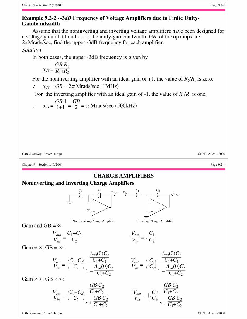
SECTION 9.2 – SWITCHED CAPACITOR AMPLIFIERSCONTINUOUS TIME AMPLIFIERS
Inverting and Noninverting Amplifiers
+-
R1 R2 vOUT
vIN +-
R1 R2 vOUTvIN
Fig. 9.2-01
Gain and GB = ∞:VoutVin =
R1+R2R1
VoutVin = -
R2 R1
Gain ≠ ∞, GB = ∞:
Vout(s)Vin(s) =
R1+R2
R1
Avd(0)R1R1+R2
1 + Avd(0)R1R1+R2
Vout(s)Vin(s) = -
R2
R1
R1Avd(0)R1+R2
1 + Avd(0)R1R1+R2
Gain ≠ ∞, GB ≠ ∞:
Vout(s)Vin(s) =
R1+R2
R1
GB·R1R1+R2
s + GB·R1R1+R2
=
R1+R2
R1 ωH
s+ωH Vout(s)Vin(s) =
- R2R1
GB·R1R1+R2
s + GB·R1R1+R2
=
- R2R1
ωHs+ωH
Chapter 9 – Section 2 (5/2/04) Page 9.2-2
CMOS Analog Circuit Design © P.E. Allen - 2004
Example 9.2-1- Accuracy Limitation of Voltage Amplifiers due to a Finite VoltageGain
Assume that the noninverting and inverting voltage amplifiers have been designed fora voltage gain of +10 and -10. If Avd(0) is 1000, find the actual voltage gains for eachamplifier.Solution
For the noninverting amplifier, the ratio of R2/R1 is 9.
Avd(0)R1/(R1+R2) = 10001+9 = 100.
∴ VoutVin
= 10
100
101 = 9.901 rather than 10.
For the inverting amplifier, the ratio of R2/R1 is 10.Avd(0)R1R1+R2
= 10001+10 = 90.909
∴ VoutVin
= -(10)
90.909
1+90.909 = - 9.891 rather than -10.
Chapter 9 – Section 2 (5/2/04) Page 9.2-3
CMOS Analog Circuit Design © P.E. Allen - 2004
Example 9.2-2 - -3dB Frequency of Voltage Amplifiers due to Finite Unity-Gainbandwidth
Assume that the noninverting and inverting voltage amplifiers have been designed fora voltage gain of +1 and -1. If the unity-gainbandwidth, GB, of the op amps are2πMrads/sec, find the upper -3dB frequency for each amplifier.Solution
In both cases, the upper -3dB frequency is given by
ωH = GB·R1R1+R2
For the noninverting amplifier with an ideal gain of +1, the value of R2/R1 is zero.∴ ωH = GB = 2π Mrads/sec (1MHz)
For the inverting amplifier with an ideal gain of -1, the value of R2/R1 is one.
∴ ωH = GB·11+1 =
GB2 = π Mrads/sec (500kHz)
Chapter 9 – Section 2 (5/2/04) Page 9.2-4
CMOS Analog Circuit Design © P.E. Allen - 2004
CHARGE AMPLIFIERSNoninverting and Inverting Charge Amplifiers
+
-
vIN
OUTvC1 C2
Noninverting Charge Amplifier
+
-
vINOUTv
Inverting Charge Amplifier
C1 C2
Gain and GB = ∞:VoutVin
= C1+C2
C2
VoutVin
= - C1C2
Gain ≠ ∞, GB = ∞:
Vout
Vin =
C1+C2
C2
Avd(0)C2C1+C2
1 + Avd(0)C2C1+C2
Vout
Vin =
-C1
C2
Avd(0)C2C1+C2
1 + Avd(0)C2C1+C2
Gain ≠ ∞, GB ≠ ∞:
Vout
Vin =
C1+C2
C2
GB·C2C1+C2
s + GB·C2C1+C2
Vout
Vin =
-C1
C2
GB·C2C1+C2
s + GB·C2C1+C2
Chapter 9 – Section 2 (5/2/04) Page 9.2-5
CMOS Analog Circuit Design © P.E. Allen - 2004
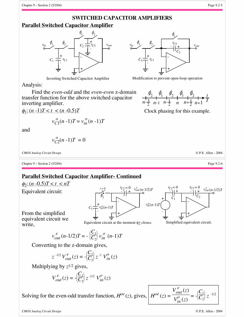
SWITCHED CAPACITOR AMPLIFIERSParallel Switched Capacitor Amplifier
1 2
+
-
1 2
voutinv
C1
2C
Inverting Switched Capacitor Amplifier
+-
vC1
vC2
+-
1 2
+
-
1
2C
C1
voutinv
Modification to prevent open-loop operation
vC1
vC2
+-
+-
Analysis:Find the even-odd and the even-even z-domain
transfer function for the above switched capacitorinverting amplifier.φ1: (n -1)T < t < (n -0.5)T
v oC1(n -1)T = v o
in (n -1)T
and
v oC2(n -1)T = 0
Clock phasing for this example.
tTn-1n-3
2 n-12 n+1
2n
1 12 2 2
n+1
Chapter 9 – Section 2 (5/2/04) Page 9.2-6
CMOS Analog Circuit Design © P.E. Allen - 2004
Parallel Switched Capacitor Amplifier- Continuedφ2: (n -0.5)T < t < nT
Equivalent circuit:
From the simplifiedequivalent circuit wewrite,
v e out (n-1/2)T = -
C1
C2 v o
in (n-1)T
Converting to the z-domain gives,
z -1/2 V e out (z) = -
C1
C2 z -1 Vo
in (z)
Multiplying by z1/2 gives,
V e out (z) = -
C1
C2 z -1/ 2 Vo
in (z)
Solving for the even-odd transfer function, Hoe (z), gives, Hoe
(z) = V e
out (z)
Vo in (z)
= -
C1
C2 z -1/ 2
inv o
+
-2CC1
Simplified equivalent circuit.
vC1 vC2
+
-
+-+-
(n-1)T
= 0 = 0 vout (n-1/2)Te
Equivalent circuit at the moment φ2 closes.
+
-C1 inv
vC2
+-
(n-1)T
= 0
o
+-
2
t = 0 vout (n-1/2)Te
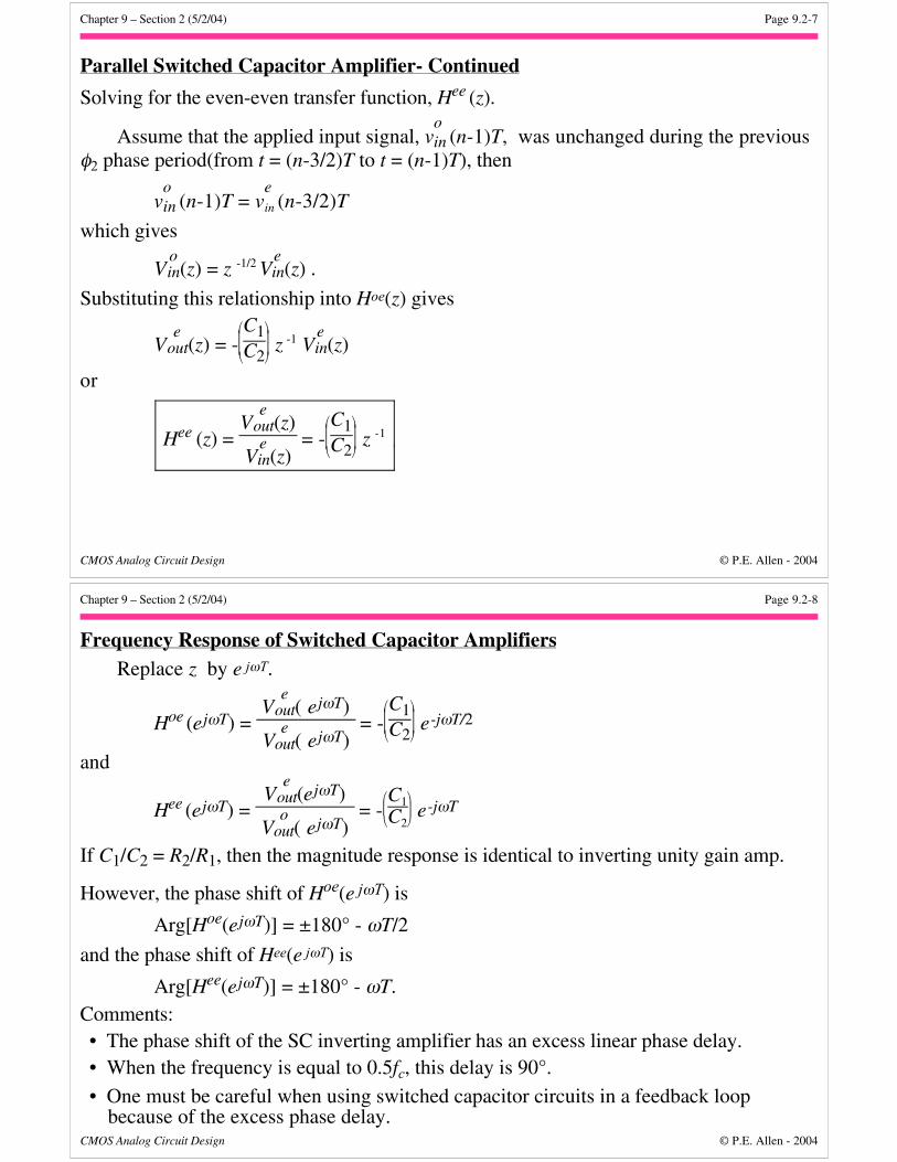
Chapter 9 – Section 2 (5/2/04) Page 9.2-7
CMOS Analog Circuit Design © P.E. Allen - 2004
Parallel Switched Capacitor Amplifier- Continued
Solving for the even-even transfer function, Hee (z).
Assume that the applied input signal, voin (n-1)T, was unchanged during the previous
φ2 phase period(from t = (n-3/2)T to t = (n-1)T), then
voin (n-1)T = v
ein (n-3/2)T
which gives
Voin(z) = z -1/2 V
ein(z) .
Substituting this relationship into Hoe(z) gives
Ve
out(z) = -
C1
C2 z -1 V
ein(z)
or
Hee (z) = V
eout(z)
Vein(z)
= -
C1
C2 z -1
Chapter 9 – Section 2 (5/2/04) Page 9.2-8
CMOS Analog Circuit Design © P.E. Allen - 2004
Frequency Response of Switched Capacitor AmplifiersReplace z by e jωT.
Hoe (e jωT) =
Ve
out( e jωT)
Ve
out( e jωT) = -
C1
C2 e -jωT/2
and
Hee (e jωT) =
Ve
out(e jωT)
Vo
out( e jωT) = -
C1
C2 e -jωT
If C1/C2 = R2/R1, then the magnitude response is identical to inverting unity gain amp.
However, the phase shift of Hoe(e jωT) is
Arg[Hoe(e jωT)] = ±180° - ωT/2
and the phase shift of Hee(e jωT) is
Arg[Hee(e jωT)] = ±180° - ωT.Comments:• The phase shift of the SC inverting amplifier has an excess linear phase delay.• When the frequency is equal to 0.5fc, this delay is 90°.
• One must be careful when using switched capacitor circuits in a feedback loopbecause of the excess phase delay.
Chapter 9 – Section 2 (5/2/04) Page 9.2-9
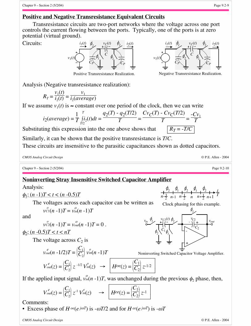
CMOS Analog Circuit Design © P.E. Allen - 2004
Positive and Negative Transresistance Equivalent CircuitsTransresistance circuits are two-port networks where the voltage across one port
controls the current flowing between the ports. Typically, one of the ports is at zeropotential (virtual ground).Circuits:
Analysis (Negative transresistance realization):
RT = v1(t)i2(t) =
v1
i2(average)
If we assume v1(t) is ≈ constant over one period of the clock, then we can write
i2(average) = 1T ⌡⌠
T/2
T
i2(t)dt = q2(T) - q2(T/2)
T = CvC(T) - CvC(T/2)
T = -Cv1
T
Substituting this expression into the one above shows that RT = -T/C
Similarly, it can be shown that the positive transresistance is T/C.These circuits are insensitive to the parasitic capacitances shown as dotted capacitors.
Positive Transresistance Realization.
1
2 2
1C
vC(t)
v1(t)
i1(t) i2(t)
CP CP
Negative Transresistance Realization.
1
2
2
1C
vC(t)
v1(t)
i1(t) i2(t)
CP CP
Chapter 9 – Section 2 (5/2/04) Page 9.2-10
CMOS Analog Circuit Design © P.E. Allen - 2004
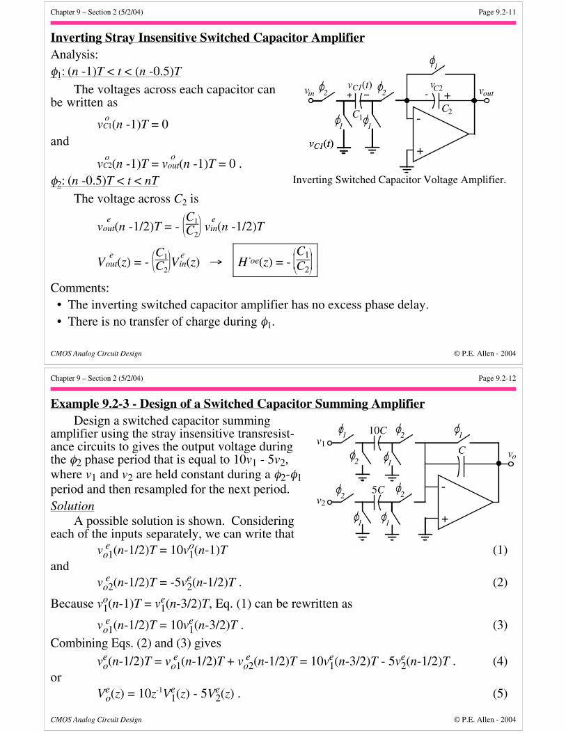
Noninverting Stray Insensitive Switched Capacitor AmplifierAnalysis:φ1: (n -1)T < t < (n -0.5)T
The voltages across each capacitor can be written as
vo
C1(n -1)T = voin(n -1)T
and
vo
C2(n -1)T = vo
out(n -1)T = 0 .φ2: (n -0.5)T < t < nT
The voltage across C2 is
ve
out(n -1/2)T =
C1
C2 v
oin(n -1)T
Ve
out(z) =
C1
C2 z -1/2 V
oin(z) → Hoe(z) =
C1
C2 z-1/2
If the applied input signal, voin(n -1)T, was unchanged during the previous φ2 phase, then,
Ve
out(z) =
C1
C2 z-1 V
ein(z) → Hee(z) =
C1
C2 z-1
Comments:• Excess phase of H oe(e jωT) is -ωT/2 and for H ee(e jωT) is -ωT
Clock phasing for this example.
tTn-1n-3
2 n-12 n+1
2n
1 12 2 2
n+1
Noninverting Switched Capacitor Voltage Amplifier.
1 2
+
-
1
2C
voutinv vC2+-
121C
vC1(t)
Chapter 9 – Section 2 (5/2/04) Page 9.2-11
CMOS Analog Circuit Design © P.E. Allen - 2004
Inverting Stray Insensitive Switched Capacitor AmplifierAnalysis:φ1: (n -1)T < t < (n -0.5)T
The voltages across each capacitor canbe written as
vo
C1(n -1)T = 0and
vo
C2(n -1)T = vo
out(n -1)T = 0 .φ2: (n -0.5)T < t < nT
The voltage across C2 is
ve
out(n -1/2)T = -
C1
C2 v
ein(n -1/2)T
Ve
out(z) = -
C1
C2V
ein(z) → H˚oe(z) = -
C1
C2
Comments: • The inverting switched capacitor amplifier has no excess phase delay. • There is no transfer of charge during φ1.
Inverting Switched Capacitor Voltage Amplifier.
1
2
+
-
1
2C
voutinv vC2+-
1
2
vC1(t)vC1(t)
1C
vC1(t)
Chapter 9 – Section 2 (5/2/04) Page 9.2-12
CMOS Analog Circuit Design © P.E. Allen - 2004
Example 9.2-3 - Design of a Switched Capacitor Summing AmplifierDesign a switched capacitor summing
amplifier using the stray insensitive transresist-ance circuits to gives the output voltage duringthe φ2 phase period that is equal to 10v1 - 5v2,where v1 and v2 are held constant during a φ2-φ1period and then resampled for the next period.Solution
A possible solution is shown. Consideringeach of the inputs separately, we can write that
v eo1(n-1/2)T = 10vo
1(n-1)T (1)and
v eo2(n-1/2)T = -5ve
2(n-1/2)T . (2)
Because vo1(n-1)T = ve
1(n-3/2)T, Eq. (1) can be rewritten as
v eo1(n-1/2)T = 10ve
1(n-3/2)T . (3)
Combining Eqs. (2) and (3) gives
veo(n-1/2)T = v e
o1(n-1/2)T + v eo2(n-1/2)T = 10ve
1(n-3/2)T - 5ve2(n-1/2)T . (4)
orVe
o(z) = 10z-1Ve1(z) - 5Ve
2(z) . (5)
1 2
+
-
1
vo12
v1
1
2
1
2v2
C
10C
5C
Chapter 9 – Section 2 (5/2/04) Page 9.2-13
CMOS Analog Circuit Design © P.E. Allen - 2004
NONIDEALITIES OF SWITCHED CAPACITOR CIRCUITSSwitchesCovered in Chapter 4.CapacitorsCovered in Chapter 2.
Chapter 9 – Section 2 (5/2/04) Page 9.2-14
CMOS Analog Circuit Design © P.E. Allen - 2004
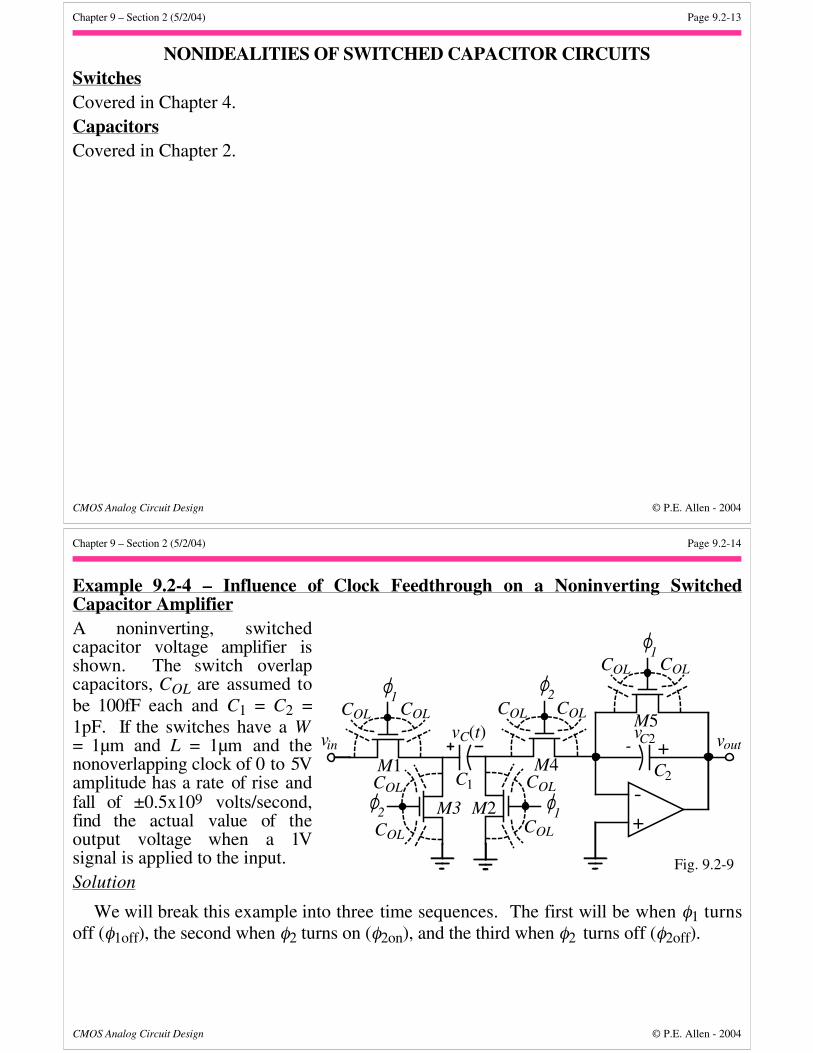
Example 9.2-4 – Influence of Clock Feedthrough on a Noninverting SwitchedCapacitor AmplifierA noninverting, switchedcapacitor voltage amplifier isshown. The switch overlapcapacitors, COL are assumed tobe 100fF each and C1 = C2 =1pF. If the switches have a W= 1µm and L = 1µm and thenonoverlapping clock of 0 to 5Vamplitude has a rate of rise andfall of ±0.5x10⁹ volts/second,find the actual value of theoutput voltage when a 1Vsignal is applied to the input.Solution
We will break this example into three time sequences. The first will be when φ1 turnsoff (φ1off), the second when φ2 turns on (φ2on), and the third when φ2 turns off (φ2off).
2
2C
voutinv vC2+-vC(t)
2
COL COL
1
COL
COL
1COL COL
COL
COL
1COL COL
M1
M3 M2
M4
M5
1C
+-
Fig. 9.2-9
Chapter 9 – Section 2 (5/2/04) Page 9.2-15
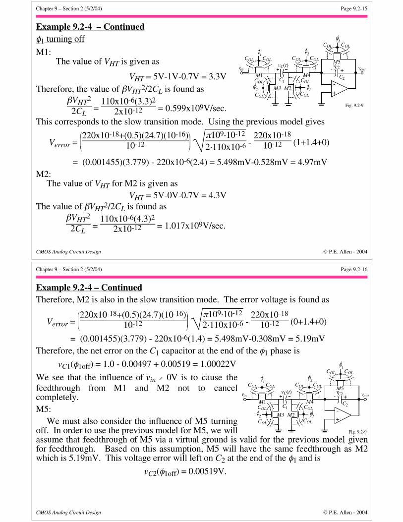
CMOS Analog Circuit Design © P.E. Allen - 2004
Example 9.2-4 – Continuedφ1 turning off
M1:The value of VHT is given as
VHT = 5V-1V-0.7V = 3.3VTherefore, the value of βVHT2/2CL is found as
βVHT2
2CL =
110x10-6(3.3)2
2x10-12 = 0.599x10⁹V/sec.
This corresponds to the slow transition mode. Using the previous model gives
Verror =
220x10-18+(0.5)(24.7)(10-16)
10-12 π109·10-12
2·110x10-6 - 220x10-18
10-12 (1+1.4+0)
= (0.001455)(3.779) - 220x10-6(2.4) = 5.498mV-0.528mV = 4.97mVM2:
The value of VHT for M2 is given asVHT = 5V-0V-0.7V = 4.3V
The value of βVHT2/2CL is found asβVHT2
2CL =
110x10-6(4.3)2
2x10-12 = 1.017x10⁹V/sec.
2
2C
voutinv vC2+-vC(t)
2
COL COL
1
COL
COL
1COL COL
COL
COL
1COL COL
M1
M3 M2
M4
M5
1C
+-
Fig. 9.2-9
Chapter 9 – Section 2 (5/2/04) Page 9.2-16
CMOS Analog Circuit Design © P.E. Allen - 2004
Example 9.2-4 – ContinuedTherefore, M2 is also in the slow transition mode. The error voltage is found as
Verror =
220x10-18+(0.5)(24.7)(10-16)
10-12 π109·10-12
2·110x10-6 - 220x10-18
10-12 (0+1.4+0)
= (0.001455)(3.779) - 220x10-6(1.4) = 5.498mV-0.308mV = 5.19mVTherefore, the net error on the C1 capacitor at the end of the φ1 phase is
vC1(φ1off) = 1.0 - 0.00497 + 0.00519 = 1.00022V
We see that the influence of vin ≠ 0V is to cause thefeedthrough from M1 and M2 not to cancelcompletely.M5:
We must also consider the influence of M5 turningoff. In order to use the previous model for M5, we willassume that feedthrough of M5 via a virtual ground is valid for the previous model givenfor feedthrough. Based on this assumption, M5 will have the same feedthrough as M2which is 5.19mV. This voltage error will left on C2 at the end of the φ1 and is
vC2(φ1off) = 0.00519V.
2
2C
voutinv vC2+-vC(t)
2
COL COL
1
COL
COL
1COL COL
COL
COL
1COL COL
M1
M3 M2
M4
M5
1C
+-
Fig. 9.2-9
Chapter 9 – Section 2 (5/2/04) Page 9.2-17
CMOS Analog Circuit Design © P.E. Allen - 2004
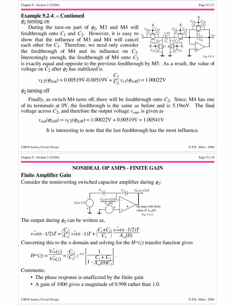
Example 9.2-4 – Continuedφ2 turning on
During the turn-on part of φ2, M3 and M4 willfeedthrough onto C1 and C2. However, it is easy toshow that the influence of M3 and M4 will canceleach other for C1. Therefore, we need only considerthe feedthrough of M4 and its influence on C2.Interestingly enough, the feedthrough of M4 onto C2is exactly equal and opposite to the previous feedthrough by M5. As a result, the value ofvoltage on C2 after φ2 has stabilized is
vC2(φ2on) = 0.00519V-0.00519V + C1C2
vc1(φ1off) = 1.00022V
φ2 turning off
Finally, as switch M4 turns off, there will be feedthrough onto C2. Since, M4 has oneof its terminals at 0V, the feedthrough is the same as before and is 5.19mV. The finalvoltage across C2, and therefore the output voltage vout, is given as
vout(φ2off) = vC2(φ2off) = 1.00022V + 0.00519V = 1.00541V
It is interesting to note that the last feedthrough has the most influence.
2
2C
voutinv vC2+-vC(t)
2
COL COL
1
COL
COL
1COL COL
COL
COL
1COL COL
M1
M3 M2
M4
M5
1C
+-
Fig. 9.2-9
Chapter 9 – Section 2 (5/2/04) Page 9.2-18
CMOS Analog Circuit Design © P.E. Allen - 2004
NONIDEAL OP AMPS - FINITE GAINFinite Amplifier GainConsider the noninverting switched capacitor amplifier during φ2:
inv
+
-
2CC1
+
-
(n-1)T
vout (n-1/2)Te
ovout (n-1/2)T
e
Avd(0)+- Op amp with finite
value of Avd(0)Fig. 9.2-11
The output during φ2 can be written as,
ve
out(n -1/2)T =
C1
C2 v
oin(n -1)T +
C1+C2
C2 v
eout(n -1/2)T
Avd(0)
Converting this to the z-domain and solving for the Hoe(z) transfer function gives
Hoe(z) = V
eout(z)
Voin(z)
=
C1
C2 z-1/2
1
1 - C1 + C2
Avd(0)C2
.
Comments:• The phase response is unaffected by the finite gain• A gain of 1000 gives a magnitude of 0.998 rather than 1.0.

Chapter 9 – Section 2 (5/2/04) Page 9.2-19
CMOS Analog Circuit Design © P.E. Allen - 2004
Nonideal Op Amps - Finite Bandwidth and Slew RateFinite GB:
• In general the analysis is complicated. (We will provide more detail for integrators.)• The clock period, T, should be equal to or less that 10/GB.• The settling time of the op amp must be less that T/2.
Slew Rate:• The slew rate of the op amp should be large enough so that the op amp can make a
full swing within T/2.
Chapter 9 – Section 2 (5/2/04) Page 9.2-20
CMOS Analog Circuit Design © P.E. Allen - 2004
SUMMARY• Continuous time amplifiers are influenced by the gain and gainbandwidth of the op amp• Charge amplifiers are also influenced by the gain and the gainbandwidth of the op amp• Switched capacitor amplifiers replace the resistors of the continuous time amplifier with
switched capacitor equivalents• The transresistor SC amplifiers can be inverting and noninverting with the positive
input terminal of the op amp on ground• The nonidealities of the SC amplifier include:
- Switches
- Capacitors
- Op amp finite gain
- Op amp finite GB
Chapter 9 – Section 3 (5/2/04) Page 9.3-1
CMOS Analog Circuit Design © P.E. Allen - 2004
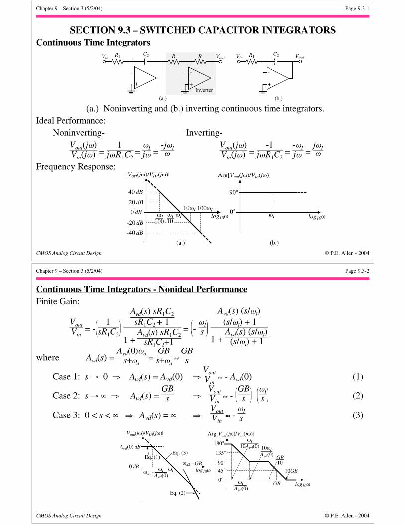
SECTION 9.3 – SWITCHED CAPACITOR INTEGRATORSContinuous Time Integrators
-R1 C2 R R VoutVin
(a.)
+
-
+
-
Inverter
(b.)
R1 C2Vin Vout
+
-
(a.) Noninverting and (b.) inverting continuous time integrators.Ideal Performance:
Noninverting- Inverting-Vout(jω)Vin(jω) =
1jω R 1C2
= ωI
jω = -jωIω
Vout(jω)Vin(jω) =
-1jω R 1C2
= -ωI
jω = jωIω
Frequency Response:
90°
0°
Arg[Vout(jω)/Vin(jω)]
ωI log10ω
|Vout(jω)/Vin(jω)|
ωIωIωI100 10
10ωI 100ωI
log10ω
40 dB
20 dB
0 dB
-20 dB
-40 dB
(a.) (b.)
Chapter 9 – Section 3 (5/2/04) Page 9.3-2
CMOS Analog Circuit Design © P.E. Allen - 2004
Continuous Time Integrators - Nonideal PerformanceFinite Gain:
Vout
Vin = -
1
sR1C2
Avd(s) sR1C2
sR1C2 + 1
1 + Avd(s) sR1C2
sR1C2+1
=
- ωI
s
Avd(s) (s/ωΙ) (s/ωΙ) + 1
1 + Avd(s) (s/ωΙ) (s/ωΙ) + 1
where Avd(s) = Avd(0)ωa
s+ωa =
GBs+ωa
≈ GBs
Case 1: s → 0 ⇒ Avd(s) = Avd(0) ⇒Vout
Vin ≈ - Avd(0) (1)
Case 2: s → ∞ ⇒ Avd(s) = GBs ⇒
Vout
Vin ≈ -
GB
s
ωI
s (2)
Case 3: 0 < s < ∞ ⇒ Avd(s) = ∞ ⇒ Vout
Vin ≈ -
ωI
s (3)
90°
0°
Arg[Vout(jω)/Vin(jω)]
log10ωωI
Avd(0)GB
180°
45°
135°
ωI10Avd(0) 10ωI
Avd(0)GB10
10GB
|Vout(jω)/Vin(jω)|
ωI log10ω0 dB GB
Avd(0) dBEq. (3)
Eq. (2)
Eq. (1)
ωIAvd(0)
ωx1 =
ωx2 =
Chapter 9 – Section 3 (5/2/04) Page 9.3-3
CMOS Analog Circuit Design © P.E. Allen - 2004
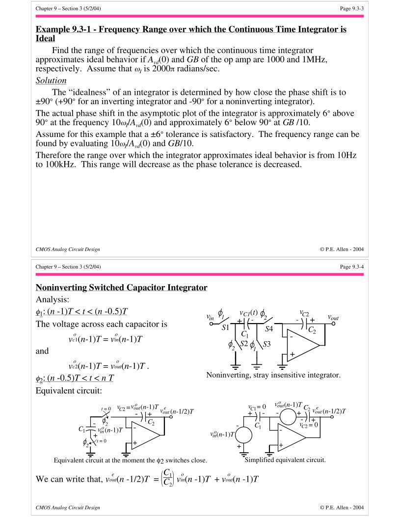
Example 9.3-1 - Frequency Range over which the Continuous Time Integrator isIdeal
Find the range of frequencies over which the continuous time integratorapproximates ideal behavior if Avd(0) and GB of the op amp are 1000 and 1MHz,respectively. Assume that ωI is 2000π radians/sec.Solution
The “idealness” of an integrator is determined by how close the phase shift is to±90° (+90° for an inverting integrator and -90° for a noninverting integrator).The actual phase shift in the asymptotic plot of the integrator is approximately 6° above90° at the frequency 10ωI/Avd(0) and approximately 6° below 90° at GB /10.Assume for this example that a ±6° tolerance is satisfactory. The frequency range can befound by evaluating 10ωI/Avd(0) and GB/10.Therefore the range over which the integrator approximates ideal behavior is from 10Hzto 100kHz. This range will decrease as the phase tolerance is decreased.
Chapter 9 – Section 3 (5/2/04) Page 9.3-4
CMOS Analog Circuit Design © P.E. Allen - 2004
Noninverting Switched Capacitor IntegratorAnalysis:φ1: (n -1)T < t < (n -0.5)T
The voltage across each capacitor is
voc1(n-1)T = v
oin(n-1)T
and
voc2(n-1)T = v
oout(n-1)T .
φ2: (n -0.5)T < t < n T
Equivalent circuit:
oinv
Simplified equivalent circuit.
2C
C1
vC1
+
++
(n-1)T
= 0
vC2 = 0
vout (n-1/2)Te
+--
-vout(n-1)To
-
+
-
Equivalent circuit at the moment the φ2 switches close.
C1 inv+
(n-1)T
vC2 =
o
vout(n-1)To
+2
t = 0 vout (n-1/2)Te
--
+
-
t = 02
2C
We can write that, ve
out(n -1/2)T =
C1
C2 v
oin(n -1)T + v
oout(n -1)T
Noninverting, stray insensitive integrator.
1 2
2C
voutinv vC2+-
12
1C
vC1(t)
+
-+ -
S1
S2 S3
S4
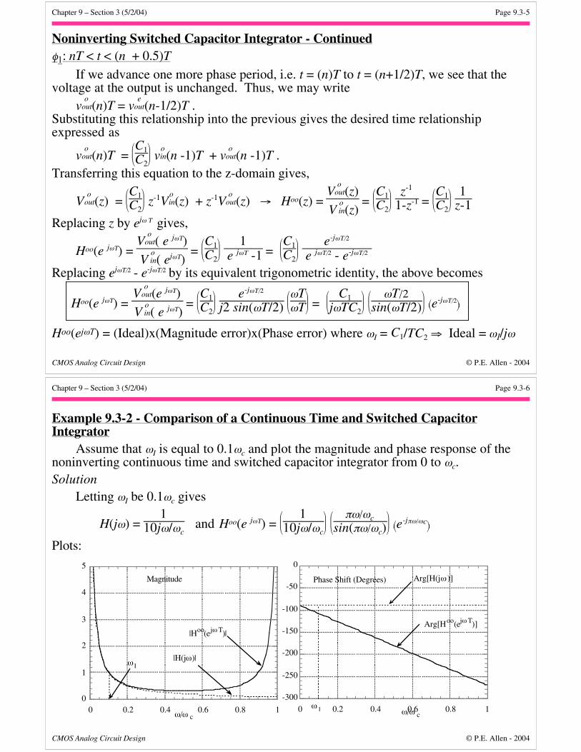
Chapter 9 – Section 3 (5/2/04) Page 9.3-5
CMOS Analog Circuit Design © P.E. Allen - 2004
Noninverting Switched Capacitor Integrator - Continuedφ1: nT < t < (n + 0.5)T
If we advance one more phase period, i.e. t = (n)T to t = (n+1/2)T, we see that thevoltage at the output is unchanged. Thus, we may write
vo
out(n)T = ve
out(n-1/2)T .Substituting this relationship into the previous gives the desired time relationshipexpressed as
vo
out(n)T =
C1
C2 v
oin(n -1)T + v
oout(n -1)T .
Transferring this equation to the z-domain gives,
Vo
out(z) =
C1
C2 z-1V
oin(z) + z-1V
oout(z) → Hoo(z) =
Vo
out(z) V
oin(z)
=
C1
C2
z-1
1-z-1 =
C1
C2
1z-1
Replacing z by ejω Τ gives,
Hoo(e jωΤ) = V
oout( e jωΤ)
Voin( ejωΤ)
=
C1
C2
1 e jωΤ -1 =
C1
C2
e-jωΤ/2
e jωΤ/2 - e-jωΤ/2 Replacing ejωΤ/2 - e-jωΤ/2 by its equivalent trigonometric identity, the above becomes
Hoo(e jωΤ) = V
oout(e jωΤ)
Voin( e jωΤ)
=
C1
C2
e-jωΤ/2
j2 sin(ωT/2)
ωT
ωT =
C1
jωTC2
ωT/2
sin(ωT/2) e-jωΤ/2
Hoo(ejωT) = (Ideal)x(Magnitude error)x(Phase error) where ωI = C1/TC2 ⇒ Ideal = ωI/jω
Chapter 9 – Section 3 (5/2/04) Page 9.3-6
CMOS Analog Circuit Design © P.E. Allen - 2004
Example 9.3-2 - Comparison of a Continuous Time and Switched CapacitorIntegrator
Assume that ωI is equal to 0.1ωc and plot the magnitude and phase response of thenoninverting continuous time and switched capacitor integrator from 0 to ωc.Solution
Letting ωI be 0.1ωc gives
H(jω) = 1
10jω/ωc and Hoo(e jωΤ) =
1
10jω/ωc
πω/ωc
sin(πω/ωc) e-jπω/ωc
Plots:
0
1
2
3
4
5
0 0.2 0.4 0.6 0.8 1
Magnitude
|Hoo(ejωT)|
|H(jω)|ω I
ω/ω c
-300
-250
-200
-150
-100
-50
0
0 0.2 0.4 0.6 0.8 1
Phase Shift (Degrees)
Arg[Hoo(ejωT)]
Arg[H(jω)]
ω I ω/ω c
Chapter 9 – Section 3 (5/2/04) Page 9.3-7
CMOS Analog Circuit Design © P.E. Allen - 2004
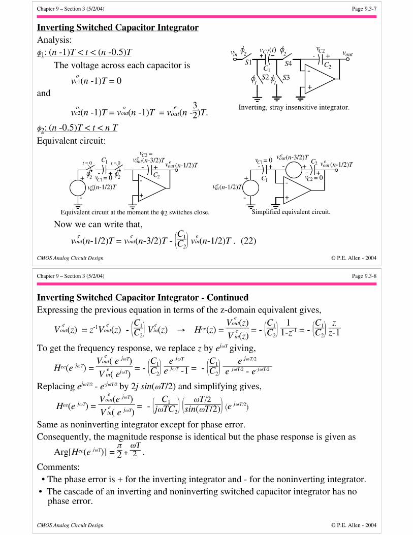
Inverting Switched Capacitor IntegratorAnalysis:φ1: (n -1)T < t < (n -0.5)T
The voltage across each capacitor is
voc1(n -1)T = 0
and
voc2(n -1)T = v
oout(n -1)T = v
eout(n -
32)T.
φ2: (n -0.5)T < t < n T
Equivalent circuit:
einv
Simplified equivalent circuit.
2C
C1
vC1
++
+
(n-1/2)T
= 0
vC2 = 0
vout (n-1/2)Te
+--
-vout(n-3/2)Te
- +
-
Equivalent circuit at the moment the φ2 switches close.
vC2 =vout(n-3/2)Te
+2
t = 0 vout (n-1/2)Te
-
+
-
C1
vC1+ +
(n-1/2)T= 0
-
-
einv
2
t = 0
2C
Now we can write that,
ve
out(n-1/2)T = ve
out(n-3/2)T -
C1
C2 v
ein(n-1/2)T . (22)
Inverting, stray insensitive integrator.
1
2
2C
voutinv vC2+-
1
2
1C
vC1(t)
+
-S1
S2 S3
S4
Chapter 9 – Section 3 (5/2/04) Page 9.3-8
CMOS Analog Circuit Design © P.E. Allen - 2004
Inverting Switched Capacitor Integrator - ContinuedExpressing the previous equation in terms of the z-domain equivalent gives,
Ve
out(z) = z-1Ve
out(z) -
C1
C2 V
ein(z) → Hee(z) =
Ve
out(z) V
ein(z)
= -
C1
C2
11-z-1 = -
C1
C2
zz-1
To get the frequency response, we replace z by ejωΤ giving,
Hee(e jωΤ) = V
eout( e jωΤ)
Vein( ejωΤ)
= -
C1
C2
e jωΤ
e jωΤ -1 = -
C1
C2
e jωΤ/2
e jωΤ/2 - e-jωΤ/2
Replacing ejωΤ/2 - e-jωΤ/2 by 2j sin(ωT/2) and simplifying gives,
Hee(e jωΤ) = V
eout(e jωΤ)
Vein( e jωΤ)
= -
C1
jωTC2
ωT/2
sin(ωT/2) e jωΤ/2
Same as noninverting integrator except for phase error.Consequently, the magnitude response is identical but the phase response is given as
Arg[Hee(e jωΤ)] = π2 +
ωΤ2 .
Comments: • The phase error is + for the inverting integrator and - for the noninverting integrator.• The cascade of an inverting and noninverting switched capacitor integrator has no
phase error.
Chapter 9 – Section 3 (5/2/04) Page 9.3-9
CMOS Analog Circuit Design © P.E. Allen - 2004
A Sign MultiplexerA circuit that changes the φ1 and φ2 of the leftmost switches of the stray insensitive,switched capacitor integrator.
1 2
VC
x
y
To switch connectedto the input signal (S1).
To the left most switchconnected to ground (S2).
VC
0
1
x y
1
12
2
Fig. 9.3-8
This circuit steers the φ1 and φ2 clocks to the input switch (S1) and the leftmost switchconnected to ground (S2) as a function of whether Vc is high or low.
Chapter 9 – Section 3 (5/2/04) Page 9.3-10
CMOS Analog Circuit Design © P.E. Allen - 2004
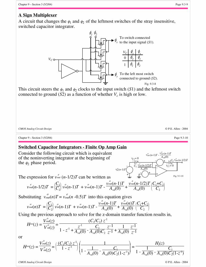
Switched Capacitor Integrators - Finite Op Amp GainConsider the following circuit which is equivalentof the noninverting integrator at the beginning ofthe φ2 phase period.
The expression for ve
out (n-1/2)T can be written as
ve
out(n-1/2)T =
C1
C2 v
oin(n-1)T + v
oout(n-1)T -
vo
out(n-1)TAvd(0) +
ve
out(n-1/2)TAvd(0)
C1+C2
C2
Substituting vo
out(n)T = ve
out(n -0.5)T into this equation gives
vo
out(n)T =
C1
C2 v
oin(n-1)T + v
oout(n-1)T -
vo
out(n-1)TAvd(0) +
vo
out(n)TAvd(0)
C1+C2
C2
Using the previous approach to solve for the z-domain transfer function results in,
Hoo(z) = V
oout(z)
Voin(z)
= (C1/C2) z
-1
1 - z-1 + z-1
Avd(0) - C1
Avd(0)C2 z-1
z-1 + 1
Avd(0) z-1
z-1
or
Hoo(z) = V
oout(z)
Voin(z)
=
(C1/C2) z
-1
1 - z-1
1
1 - 1Avd(0) -
C1
Avd(0)C2(1-z-1) =
HI(z)
1 - 1
Avd(0) - C1
Avd(0)C2(1-z-1)
oinv
2C
C1
vC1
+
++
(n-1)T
= 0
vC2 = 0
vout (n-1/2)Te
+--
-
-
+
-
+-
vout (n-1/2)Te
Avd(0)
vout (n-1)T -o vout (n-1)T
o
Avd(0)
Fig. 9.3-10
Chapter 9 – Section 3 (5/2/04) Page 9.3-11
CMOS Analog Circuit Design © P.E. Allen - 2004
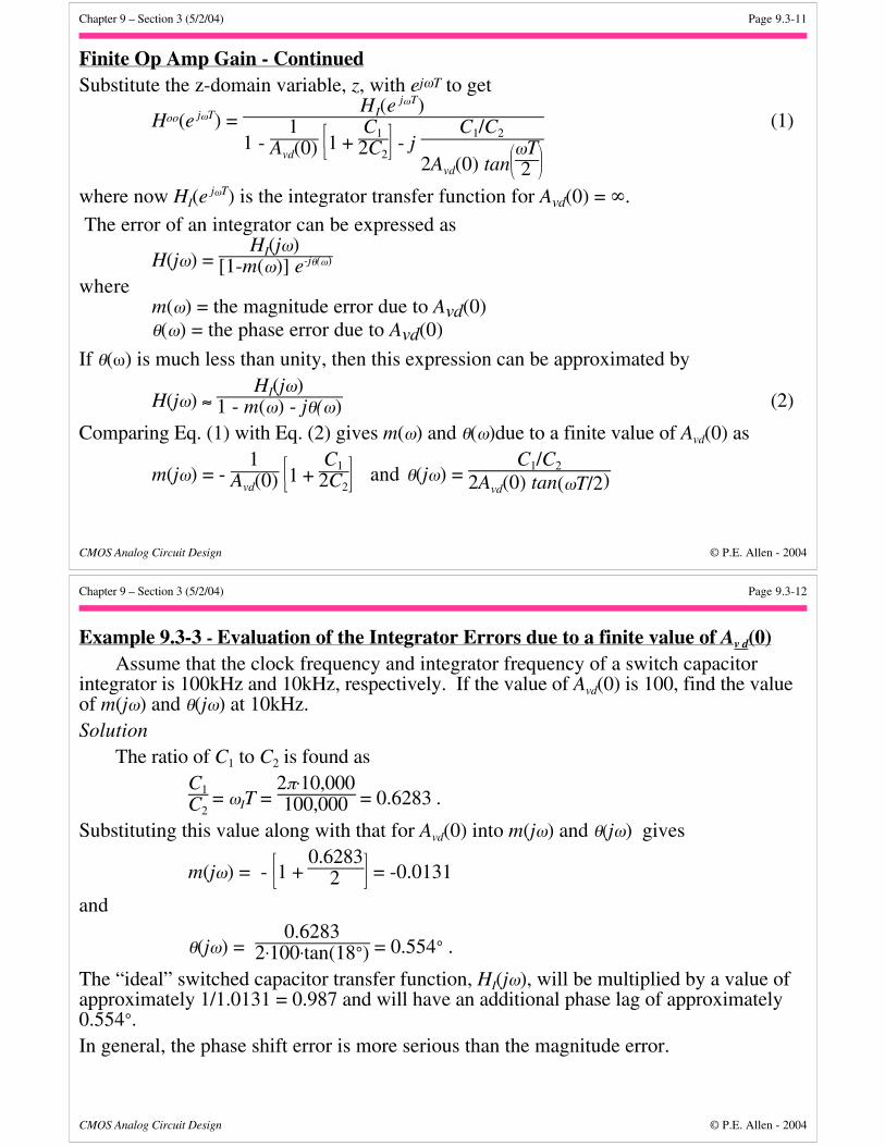
Finite Op Amp Gain - ContinuedSubstitute the z-domain variable, z, with ejωT to get
Hoo(e jωT) = HI(e
jωT)
1 - 1
Avd(0)
1 + C1
2C2 - j
C1/C2
2Avd(0) tan
ωT
2
(1)
where now HI(e jωT) is the integrator transfer function for Avd(0) = ∞.
The error of an integrator can be expressed as
H(jω) = HI(jω)
[1-m(ω)] e-jθ(ω) where
m(ω) = the magnitude error due to Avd(0)θ(ω) = the phase error due to Avd(0)
If θ(ω) is much less than unity, then this expression can be approximated by
H(jω) ≈ HI(jω)
1 - m(ω) - jθ(ω) (2)
Comparing Eq. (1) with Eq. (2) gives m(ω) and θ(ω)due to a finite value of Avd(0) as
m(jω) = - 1
Avd(0)
1 + C1
2C2 and θ(jω) =
C1/C2
2Avd(0) tan(ωT/2)
Chapter 9 – Section 3 (5/2/04) Page 9.3-12
CMOS Analog Circuit Design © P.E. Allen - 2004
Example 9.3-3 - Evaluation of the Integrator Errors due to a finite value of A v d (0)Assume that the clock frequency and integrator frequency of a switch capacitor
integrator is 100kHz and 10kHz, respectively. If the value of Avd(0) is 100, find the valueof m(jω) and θ(jω) at 10kHz.Solution
The ratio of C1 to C2 is found asC1
C2 = ωIT =
2π⋅10,000100,000 = 0.6283 .
Substituting this value along with that for Avd(0) into m(jω) and θ(jω) gives
m(jω) = -
1 + 0.6283
2 = -0.0131
and
θ(jω) = 0.6283
2⋅100⋅tan(18°) = 0.554° .
The “ideal” switched capacitor transfer function, HI(jω), will be multiplied by a value ofapproximately 1/1.0131 = 0.987 and will have an additional phase lag of approximately0.554°.In general, the phase shift error is more serious than the magnitude error.
Chapter 9 – Section 3 (5/2/04) Page 9.3-13
CMOS Analog Circuit Design © P.E. Allen - 2004
Switched Capacitor Integrators - Finite Op Amp GBThe precise analysis of the influence of GB can be found elsewhere† . The results of
such an analysis can be summarized in the following table.
NoninvertingIntegrator
Inverting Integrator
m(ω) ≈ -e-k1
C2
C1+C2
θ(ω) ≈ 0
m(ω) ≈ -e-k1
1 -
C2
C1+C2 cos(ωT)
θ(ω) ≈ -e-k1
C2
C1+C2 cos(ωT)
k1 ≈ π
C2
C1+C2
GB
fc
If ωT is much less than unity, the expressions in table reduce to
m(ω) ≈ -2π
f
fc e-π(GB/f
c)
† K. Martin and A.S. Sedra, “Effects of the Op Amp Finite Gain and Bandwidth on the Performance of Switched-Capacitor Filters,” IEEE Trans. onCircuits and Systems, vol. CAS-28, no. 8, August 1981, pp. 822-829.
Chapter 9 – Section 3 (5/2/04) Page 9.3-14
CMOS Analog Circuit Design © P.E. Allen - 2004
Switched Capacitor Circuits - kT/C NoiseSwitched capacitors generate aninherent thermal noise given bykT/C. This noise is verified asfollows.An equivalent circuit for a switchedcapacitor:The noise voltage spectral density of Fig. 9.3-11b is given as
e 2Ron = 4kTRon Volts2/Hz =
2kTRonπ Volt2/Rad./sec. (1)
The rms noise voltage is found by integrating this spectral density from 0 to ∞ to give
v 2Ron =
2kTRonπ ⌡
⌠
0
∞
ω12dω
ω12+ω2 =
2kTRonπ
πω1
2 = kTC Volts(rms)2 (2)
where ω1 = 1/(RonC). Note that the switch has an effective noise bandwidth of
fsw = 1
4RonC Hz (3)
which is found by dividing Eq. (2) by Eq. (1).
C voutvin
+
-
+
-
C voutvin
+
-
+
-
Ron
(a.) (b.)Figure 9.3-11 - (a.) Simple switched capacitor circuit. (b.) Approximation of (a.).
Chapter 9 – Section 3 (5/2/04) Page 9.3-15
CMOS Analog Circuit Design © P.E. Allen - 2004
SUMMARY• The discrete time noninverting integrator transfer function is
Hoo(e jωΤ) = V
oout(e jωΤ)
Voin( e jωΤ)
=
C1
jωTC2
ωT/2
sin(ωT/2) e-jωΤ/2
• The discrete time inverting integrator transfer function is
Hee(e jωΤ) = V
eout(e jωΤ)
Vein( e jωΤ)
= -
C1
jωTC2
ωT/2
sin(ωT/2) ejωΤ/2
• In general the integrator transfer function can be expressed as
H(ejωT) = (Ideal)x(Magnitude error)x(Phase error)• Note that the cascade of an noninverting integrator with a inverting integrator has no
phase error• A capacitor C and a switch (or switches) has a thermal noise given as kT/C where T is
the clock period
Chapter 9 – Section 4 (5/2/04) Page 9.4-1
CMOS Analog Circuit Design © P.E. Allen - 2004
SECTION 9.4 – z-DOMAIN MODELS OF TWO-PHASE SWITCHEDCAPACITOR CIRCUITS
IntroductionObjective:• Allow easy analysis of complex switched capacitor circuits• Develop methods suitable for simulation by computer• Will constrain our focus to two-phase, nonoverlapping clocksGeneral Two-Port Characterization of Switched Capacitor Circuits:
+-
vin(t) vout(t)
IndependentVoltageSource
SwitchedCapacitor
Circuit
UnswitchedCapacitor
DependentVoltageSource
Figure 9.4-1 - Two-port characterization of a general switched capacitor circuit.
Approach:• Four port - allows both phases to be examined• Two-port - simplifies the models but not as general
Chapter 9 – Section 4 (5/2/04) Page 9.4-2
CMOS Analog Circuit Design © P.E. Allen - 2004
Independent Voltage Sources
0 1/2 1 3/2 2 5/2 3 7/2 4 9/2 5t/T
v(t)v*(t)
1 2 2 2 2 21 1 1 1
v (t)O
v (t)e
0 1/2 1 3/2 2 5/2 3 7/2 4 9/2 5t/T
v(t)
1 1 1 1 1
0 1/2 1 3/2 2 5/2 3 7/2 4 9/2 5t/T
v(t)
2 2 2 2 2
2 2 2 2 2
1 1 1 1 1
Ve(z)
Vo(z)
z-1/2Vo(z)
Vo(z)
Ve(z)
z-1/2Ve(z)
Phase DependentVoltage Source
Phase IndependentVoltage Source forthe Odd Phase
Phase IndependentVoltage Source forthe Even Phase
Chapter 9 – Section 4 (5/2/04) Page 9.4-3
CMOS Analog Circuit Design © P.E. Allen - 2004
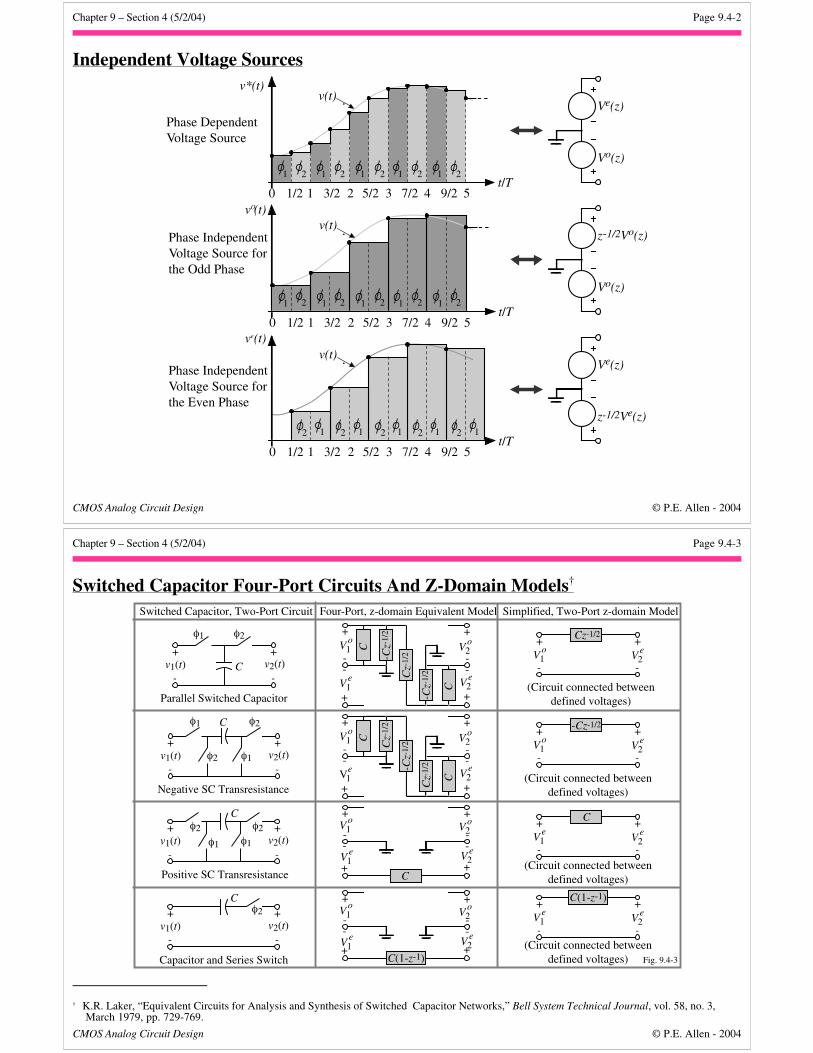
Switched Capacitor Four-Port Circuits And Z-Domain Models†
+
-V o
2
+
-V e
2
+
-V o
1
+
-V e
1
C
-Cz-
1/2
Cz-
1/2
-Cz-
1/2
C
+
-v1(t) v2(t)C
φ1 φ2
+
-
Parallel Switched Capacitor
+
-
+
-
Cz-1/2
V e2V o
1
Switched Capacitor, Two-Port Circuit Simplified, Two-Port z-domain Model
+
-v1(t) v2(t)
Cφ1 φ2
+
-
Negative SC Transresistance
φ2 φ1
+
-V o
2
+
-V e
2
+
-V o
1
+
-Ve
1
C
Cz-
1/2
-Cz-
1/2
Cz-
1/2
C
+
-
+
-
-Cz-1/2
V e2V o
1
+
-v1(t) v2(t)
C
φ1
φ2 +
-
Positive SC Transresistance
φ2φ1
+
-V o
2
+
-V e
2
+
-V o
1
+
-V e
1
C
+
-
+
-
C
V e2V e
1
+
-v1(t) v2(t)
Cφ2 +
-
Capacitor and Series Switch
+
-V o
2
+
-V e
2
+
-V o
1
+
-V e
1C(1-z-1)
+
-
+
-V e
2V e1
C(1-z-1)
Four-Port, z-domain Equivalent Model
Fig. 9.4-3
(Circuit connected betweendefined voltages)
(Circuit connected betweendefined voltages)
(Circuit connected betweendefined voltages)
(Circuit connected betweendefined voltages)
† K.R. Laker, “Equivalent Circuits for Analysis and Synthesis of Switched Capacitor Networks,” Bell System Technical Journal, vol. 58, no. 3,
March 1979, pp. 729-769.
Chapter 9 – Section 4 (5/2/04) Page 9.4-4
CMOS Analog Circuit Design © P.E. Allen - 2004
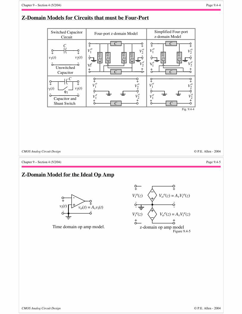
Z-Domain Models for Circuits that must be Four-Port
+
-v1(t) v2(t)
C
+
-
+
-V o
2
+
-V e
2
+
-V o
1
+
-
Ve1
C
-Cz-
1/2
Cz-
1/2
C
-Cz-
1/2
Cz-
1/2
+
-V o
2
+
-V e
2
+
-V o
1
+
-Ve
1
C
-Cz-
1/2
C
-Cz-
1/2
+
-v1(t) v2(t)
C
φ1
+
-Capacitor and Shunt Switch
+
-V o
2
+
-V e
2
+
-V o
1
+
-V e
1
C
UnswitchedCapacitor
+
-V o
2
+
-V e
2
+
-V o
1
+
-V e
1
C
Switched Capacitor Circuit
Four-port z-domain Model Simplified Four-portz-domain Model
Fig. 9.4-4
Chapter 9 – Section 4 (5/2/04) Page 9.4-5
CMOS Analog Circuit Design © P.E. Allen - 2004
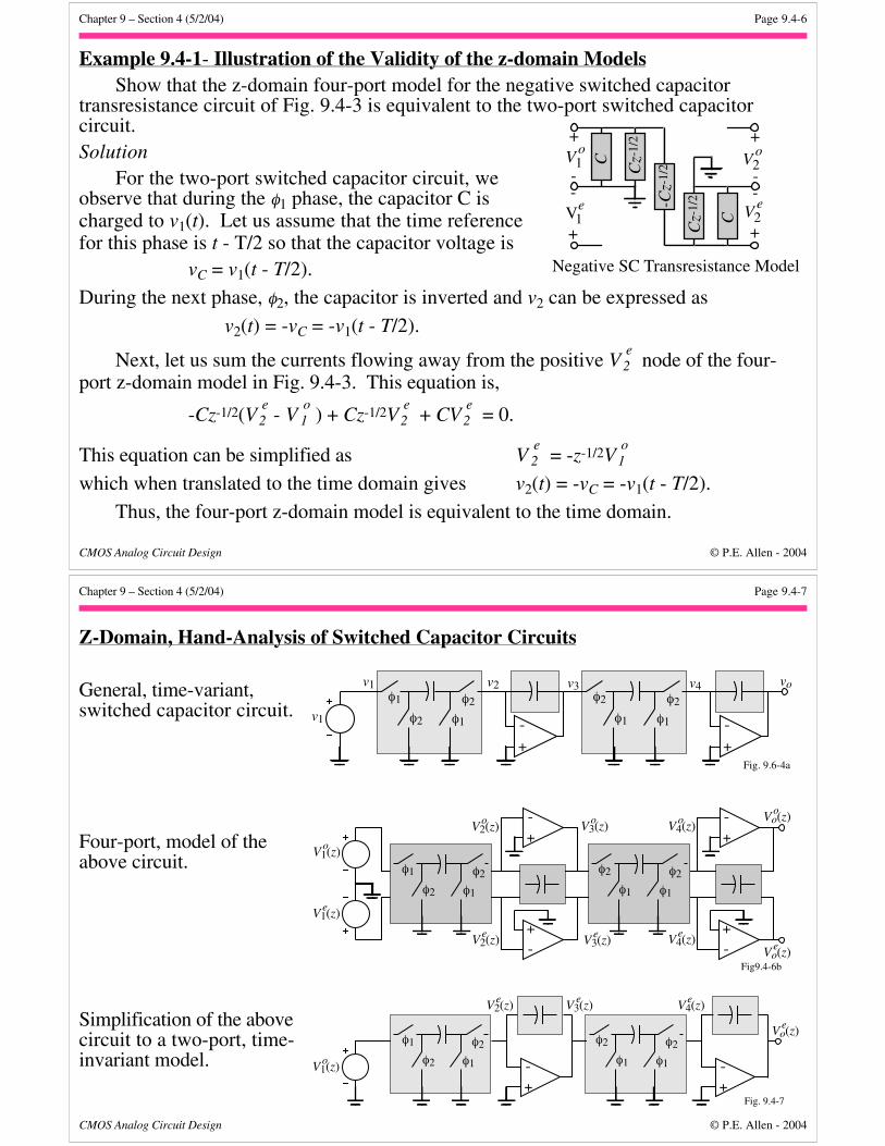
Z-Domain Model for the Ideal Op Amp
+-
+
-vi(t)
+
-vo(t) = Avvi(t)
+
-Vi
o(z)
+
-
Vie(z)
+
-Vo
o(z) = AvVio(z)
+
-
Voe(z) = AvVi
e(z)
Figure 9.4-5 Time domain op amp model. z-domain op amp model
Chapter 9 – Section 4 (5/2/04) Page 9.4-6
CMOS Analog Circuit Design © P.E. Allen - 2004
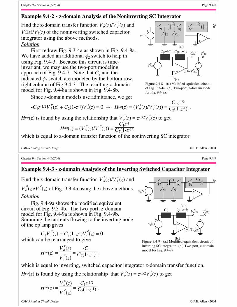
Example 9.4-1- Illustration of the Validity of the z-domain ModelsShow that the z-domain four-port model for the negative switched capacitor
transresistance circuit of Fig. 9.4-3 is equivalent to the two-port switched capacitorcircuit.Solution
For the two-port switched capacitor circuit, weobserve that during the φ1 phase, the capacitor C ischarged to v1(t). Let us assume that the time referencefor this phase is t - T/2 so that the capacitor voltage is
vC = v1(t - T/2).
During the next phase, φ2, the capacitor is inverted and v2 can be expressed as
v2(t) = -vC = -v1(t - T/2).
Next, let us sum the currents flowing away from the positive V e2 node of the four-
port z-domain model in Fig. 9.4-3. This equation is,
-Cz-1/2(V e2 - V
o1 ) + Cz-1/2V
e2 + CV
e2 = 0.
This equation can be simplified as V e2 = -z-1/2V
o1
which when translated to the time domain gives v2(t) = -vC = -v1(t - T/2).
Thus, the four-port z-domain model is equivalent to the time domain.
+
-V o
2
+
-V e
2
+
-V o
1
+
-Ve
1
C
Cz-
1/2
-Cz-
1/2
Cz-
1/2
C
Negative SC Transresistance Model
Chapter 9 – Section 4 (5/2/04) Page 9.4-7
CMOS Analog Circuit Design © P.E. Allen - 2004
Z-Domain, Hand-Analysis of Switched Capacitor Circuits
General, time-variant,switched capacitor circuit.
Four-port, model of theabove circuit.
Simplification of the abovecircuit to a two-port, time-invariant model.
+-
vov1φ1
φ1φ2
φ2
v2 v3
+-
φ2
φ1φ1
φ2
v4
v1
Fig. 9.6-4a
+-
φ1
φ1φ2
φ2 φ2
φ1φ1
φ2
V4(z)
+-
+-
+-
o Vo(z)o
V3(z)oV2(z)o
V1(z)o
V4(z)e
Vo(z)eV3(z)eV2(z)e
V1(z)e
Fig9.4-6b
+-
φ1
φ1φ2
φ2 φ2
φ1φ1
φ2
V1(z)o
V2(z)e V4(z)e
Vo(z)e
V3(z)e
+-
Fig. 9.4-7
Chapter 9 – Section 4 (5/2/04) Page 9.4-8
CMOS Analog Circuit Design © P.E. Allen - 2004
Example 9.4-2 - z-domain Analysis of the Noninverting SC Integrator
Find the z-domain transfer function V eo (z)/V oi (z) and
Voo(z)/Vo
i (z) of the noninverting switched capacitorintegrator using the above methods.Solution
First redraw Fig. 9.3-4a as shown in Fig. 9.4-8a.We have added an additional φ2 switch to help inusing Fig. 9.4-3. Because this circuit is time-invariant, we may use the two-port modelingapproach of Fig. 9.4-7. Note that C2 and theindicated φ2 switch are modeled by the bottom row,right column of Fig 9.4-3. The resulting z-domainmodel for Fig. 9.4-8a is shown in Fig. 9.4-8b.
Since z-domain models use admittance, we get
-C1z-1/2V oi (z) + C2(1-z-1)V
eo (z) = 0 → Hoe(z) = (V
eo (z)/V
oi (z)) =
C1z-1/2
C2(1-z-1) .
Hoo(z) is found by using the relationship that V oo (z) = z-1/2V
eo (z) to get
Hoo(z) = (V oo (z)/V
oi (z)) =
C1z-1
C2(1-z-1)
which is equal to z-domain transfer function of the noninverting SC integrator.
+-vi(t)
φ1
φ1φ2
φ2
+-
φ2
voC1 C2
Vi(z)
-C1z-1/2 C2(1-z-1)
o
Vo(z)e
Vo(z)o
z-1/2Vo(z)e
(a.)
(b.)Figure 9.4-8 - (a.) Modified equivalent circuit of Fig. 9.3-4a. (b.) Two-port, z-domain modelfor Fig. 9.4-8a.
Chapter 9 – Section 4 (5/2/04) Page 9.4-9
CMOS Analog Circuit Design © P.E. Allen - 2004
Example 9.4-3 - z-domain Analysis of the Inverting Switched Capacitor Integrator
Find the z-domain transfer function V eo (z)/V
ei (z) and
V oo (z)/V
ei (z) of Fig. 9.3-4a using the above methods.
SolutionFig. 9.4-9a shows the modified equivalent
circuit of Fig. 9.3-4b. The two-port, z-domainmodel for Fig. 9.4-9a is shown in Fig. 9.4-9b.Summing the currents flowing to the inverting nodeof the op amp gives
C1V ei (z) + C2(1-z-1)V
eo (z) = 0
which can be rearranged to give
Hee(z) = V
eo (z)
V ei (z)
= -C1
C2(1-z-1) .
which is equal to inverting, switched capacitor integrator z-domain transfer function.
Heo(z) is found by using the relationship that V oo (z) = z-1/2V
eo (z) to get
Heo(z) = V
oo (z)
V ei (z)
= C1z-1/2
C2(1-z-1) .
+-vi(t)
φ2
φ1φ1
φ2
+-
φ2
voC1 C2
Vi(z)
C1 C2(1-z-1)
e
Vo(z)e
Vo(z)o
z-1/2Vo(z)e
(a.)
(b.)Figure 9.4-9 - (a.) Modified equivalent circuit of inverting SC integrator. (b.) Two-port, z-domain model for Fig. 9.4-9a

Chapter 9 – Section 4 (5/2/04) Page 9.4-10
CMOS Analog Circuit Design © P.E. Allen - 2004
Example 9.4-4 - z-domain Analysis a Time-Variant Switched Capacitor Circuit
Find V oo (z) and V
eo (z) as function of V
o1 (z)
and V o2 (z) for the summing, switched capacitor
integrator of Fig. 9.4-10a.Solution
This circuit is time-variant because C3 ischarged from a different circuit for each phase.Therefore, we must use a four-port model. Theresulting z-domain model for Fig. 9.4-10a isshown in Fig. 9.4-10b.
+-v1(t)
φ1
φ1φ2
φ2
voC1 C3
v2(t)
φ1
φ2φ2
φ1
C1
Fig. 9.4-10a - Summing Integrator.
Chapter 9 – Section 4 (5/2/04) Page 9.4-11
CMOS Analog Circuit Design © P.E. Allen - 2004
Example 9.4-4 - Continued
Summing the currents flowing away from the V oi (z) node
gives
C2V o2 (z) + C3V
oo (z) - C3z-1/2V
eo (z) = 0 (1)
Summing the currents flowing away from the V ei (z) node,
-C1z-1/2V o1 (z) - C3z-1/2V
oo (z) + C3V
eo (z) = 0 (2)
Multiplying (2) by z-1/2 and adding it to (1) gives
C2V o2 (z) + C3V
oo (z) - C1z-1V
o1 (z) - C3z-1V
oo (z) = 0 (3)
Solving for V oo (z) gives,
V oo (z) =
C1z-1V o1 (z)
C3(1-z-1) - C2V
o2 (z)
C3(1-z-1)
Multiplying Eq. (1) by z-1/2 and adding it to Eq. (2) gives
C2z-1/2V o2 (z) - C1z-1V
o1 (z) - C3z-1V
eo (z) + C3V
eo (z) = 0
Solving for V eo (z) gives,
V eo (z) =
C1z-1/2V o1 (z)
C3(1-z-1) - C2z-1/2V
o2 (z)
C3(1-z-1) .
+-
V1(z)
-C1z-1/2
C3o
Vo(z)o
V2(z)o
C2
-C3z-1/2
Vi(z)o
+-C3
Vo(z)eVi(z)e
Fig. 9.4-10b - Four-port, z-domainmodel for Fig. 9.4-10a.
-C3z-1/2
Chapter 9 – Section 4 (5/2/04) Page 9.4-12
CMOS Analog Circuit Design © P.E. Allen - 2004
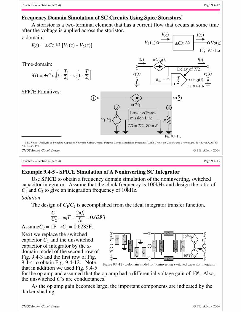
Frequency Domain Simulation of SC Circuits Using Spice Storistors†
A storistor is a two-terminal element that has a current flow that occurs at some timeafter the voltage is applied across the storistor.z-domain:
I(z) = ±Cz-1/2 [V1(z) - V2(z)]
Time-domain:
i(t) = ±C
v1
t - T2 - v2
t - T2
SPICE Primitives:
† B.D. Nelin, “Analysis of Switched-Capacitor Networks Using General-Purpose Circuit Simulation Programs,” IEEE Trans. on Circuits and Systems, pp. 43-48, vol. CAS-30,No. 1, Jan. 1983.
V1(z) V2(z)
I(z) I(z)
±Cz-1/2
Fig. 9.4-11a
+
- T2
+
-v1(t)
+ -v3(t)
+
-v2(t)
±Cv3(t)
Rin = ∞
Delay of T/2
i(t) i(t)
Fig. 9.4-11b
LosslessTrans-mission Line
TD = T/2, Z0 = R
1
V1-V2
2
±CV43 4
R
Fig. 9.4-11c
Chapter 9 – Section 4 (5/2/04) Page 9.4-13
CMOS Analog Circuit Design © P.E. Allen - 2004
Example 9.4-5 - SPICE Simulation of A Noninverting SC IntegratorUse SPICE to obtain a frequency domain simulation of the noninverting, switched
capacitor integrator. Assume that the clock frequency is 100kHz and design the ratio ofC1 and C2 to give an integration frequency of 10kHz.
SolutionThe design of C1/C2 is accomplished from the ideal integrator transfer function.
C1C2
= ωIT = 2πfIfc
= 0.6283
AssumeC2 = 1F →C1 = 0.6283F.
Next we replace the switchedcapacitor C1 and the unswitchedcapacitor of integrator by the z-domain model of the second row ofFig. 9.4-3 and the first row of Fig.9.4-4 to obtain Fig. 9.4-12. Notethat in addition we used Fig. 9.4-5for the op amp and assumed that the op amp had a differential voltage gain of 106. Also,the unswitched C’s are conductances.
As the op amp gain becomes large, the important components are indicated by thedarker shading.
+
-V o
i
+
-Ve
i
C1
C1z
-1/2
-C1z
-1/2
C1z
-1/2
C1
+
-V o
o
+
-V e
o
C2
-C2z
-1/2
C2z
-1/2
-C2z
-1/2
C2z
-1/2
106V3
106V4
5
0
6
3
0
4
1
0
2
Figure 9.4-12 - z-domain model for noninverting switched capacitor integrator.
C2

Chapter 9 – Section 4 (5/2/04) Page 9.4-14
CMOS Analog Circuit Design © P.E. Allen - 2004
Example 9.4-5 - ContinuedThe SPICE input file to perform a frequency domain simulation of Fig. 9.4-12 is shownbelow.
VIN 1 0 DC 0 AC 1R10C1 1 0 1.592X10PC1 1 0 10 DELAYG10 1 0 10 0 0.6283X14NC1 1 4 14 DELAYG14 4 1 14 0 0.6283R40C1 4 0 1.592X40PC1 4 0 40 DELAYG40 4 0 40 0 0.6283X43PC2 4 3 43 DELAYG43 4 3 43 0 1R35 3 5 1.0X56PC2 5 6 56 DELAYG56 5 6 56 0 1R46 4 6 1.0X36NC2 3 6 36 DELAY
G36 6 3 36 0 1X45NC2 4 5 45 DELAYG45 5 4 45 0 1EODD 6 0 4 0 -1E6EVEN 5 0 3 0 -1E6********************.SUBCKT DELAY 1 2 3ED 4 0 1 2 1TD 4 0 3 0 ZO=1K TD=5URDO 3 0 1K.ENDS DELAY********************.AC LIN 99 1K 99K.PRINT AC V(6) VP(6) V(5) VP(5).PROBE.END
Chapter 9 – Section 4 (5/2/04) Page 9.4-15
CMOS Analog Circuit Design © P.E. Allen - 2004
Example 9.4-5 - ContinuedSimulation Results:
Mag
nitu
de
Frequency (kHz)20 40 60 80 1000
(a.)
Both H and Hoe oo
0
1
2
3
4
5
(b.)Frequency (kHz)
20 40 60 80 1000-200
-150
-100
-50
0
50
100
150
200
Phas
e Sh
ift (
Deg
rees
)
Phase of H (jw)oe
Phase of H (jw)oo
Comments:• This approach is applicable to all switched capacitor circuits that use two-phase,
nonoverlapping clocks.• If the op amp gain is large, some simplification is possible in the four-port z-domain
models.• The primary advantage of this approach is that it is not necessary to learn a new
simulator.
Chapter 9 – Section 4 (5/2/04) Page 9.4-16
CMOS Analog Circuit Design © P.E. Allen - 2004
Simulation of Switched Capacitor Circuits Using SWITCAP†
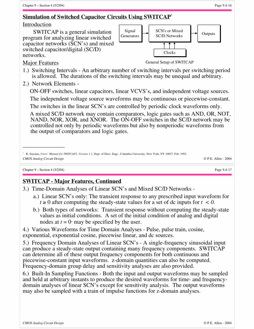
IntroductionSWITCAP is a general simulation
program for analyzing linear switchedcapacitor networks (SCN’s) and mixedswitched capacitor/digital (SC/D)networks.Major Features1.) Switching Intervals - An arbitrary number of switching intervals per switching period
is allowed. The durations of the switching intervals may be unequal and arbitrary.2.) Network Elements - ON-OFF switches, linear capacitors, linear VCVS’s, and independent voltage sources. The independent voltage source waveforms may be continuous or piecewise-constant. The switches in the linear SCN’s are controlled by periodic clock waveforms only. A mixed SC/D network may contain comparators, logic gates such as AND, OR, NOT,
NAND, NOR, XOR, and XNOR. The ON-OFF switches in the SC/D network may becontrolled not only by periodic waveforms but also by nonperiodic waveforms fromthe output of comparators and logic gates.
† K. Suyama, Users’ Manual for SWITCAP2, Version 1.1, Dept. of Elect. Engr., Columbia University, New York, NY 10027, Feb. 1992.
SignalGenerators
SCN's or MixedSC/D Networks Outputs
Clocks
General Setup of SWITCAP
Chapter 9 – Section 4 (5/2/04) Page 9.4-17
CMOS Analog Circuit Design © P.E. Allen - 2004
SWITCAP - Major Features, Continued3.) Time-Domain Analyses of Linear SCN’s and Mixed SC/D Networks -
a.) Linear SCN’s only: The transient response to any prescribed input waveform fort ≥ 0 after computing the steady-state values for a set of dc inputs for t < 0.
b.) Both types of networks: Transient response without computing the steady-statevalues as initial conditions. A set of the initial condition of analog and digitalnodes at t = 0- may be specified by the user.
4.) Various Waveforms for Time Domain Analyses - Pulse, pulse train, cosine,exponential, exponential cosine, piecewise linear, and dc sources.5.) Frequency Domain Analyses of Linear SCN’s - A single-frequency sinusoidal inputcan produce a steady-state output containing many frequency components. SWITCAPcan determine all of these output frequency components for both continuous andpiecewise-constant input waveforms. z-domain quantities can also be computed.Frequency-domain group delay and sensitivity analyses are also provided.6.) Built-In Sampling Functions - Both the input and output waveforms may be sampledand held at arbitrary instants to produce the desired waveforms for time- and frequency-domain analyses of linear SCN’s except for sensitivity analysis. The output waveformsmay also be sampled with a train of impulse functions for z-domain analyses.
Chapter 9 – Section 4 (5/2/04) Page 9.4-18
CMOS Analog Circuit Design © P.E. Allen - 2004
SWITCAP - Major Features, Continued7.) Subcircuits - Subcircuits, including analog and/or digital elements, may be definedwith symbolic values for capacitances, VCVS gains, clocks, and other parameters.Hierarchical use of subcircuits is allowed.8.) Finite Resistances, Op Amp Poles, and Switch Parasitics - Finite resistance ismodeled with SCN’s operating at clock frequencies higher than the normal clock. These“resistors” permit the modeling of op amp poles. Capacitors are added to the switchmodel to represent clock feedthrough.
Chapter 9 – Section 4 (5/2/04) Page 9.4-19
CMOS Analog Circuit Design © P.E. Allen - 2004
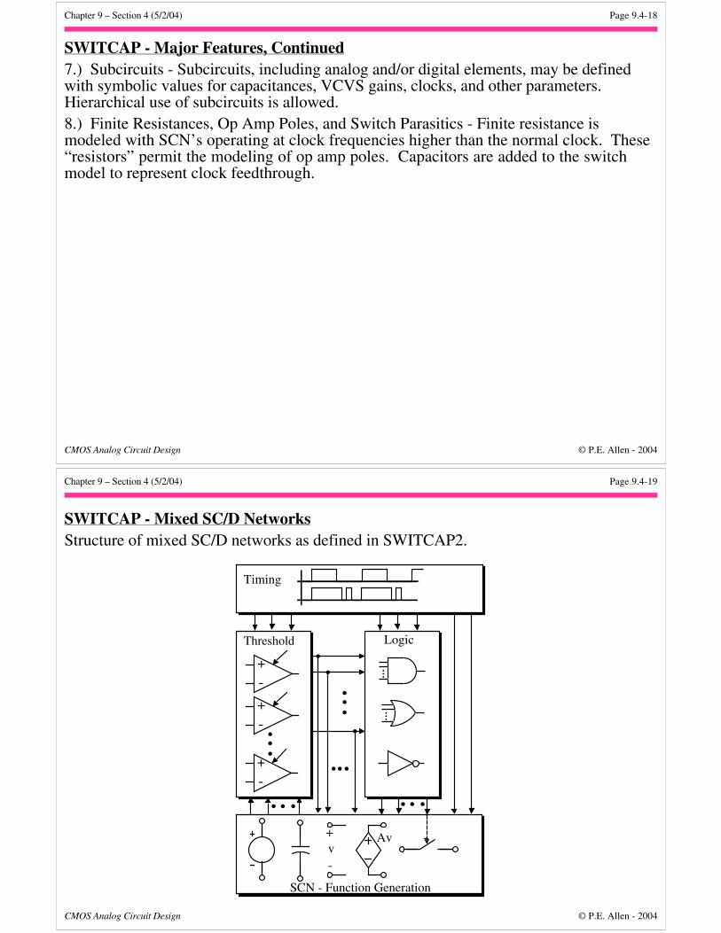
SWITCAP - Mixed SC/D NetworksStructure of mixed SC/D networks as defined in SWITCAP2.
+-+-
+-
Threshold
...
...
Logic
+
-v
Av
SCN - Function Generation
Timing
Chapter 9 – Section 4 (5/2/04) Page 9.4-20
CMOS Analog Circuit Design © P.E. Allen - 2004
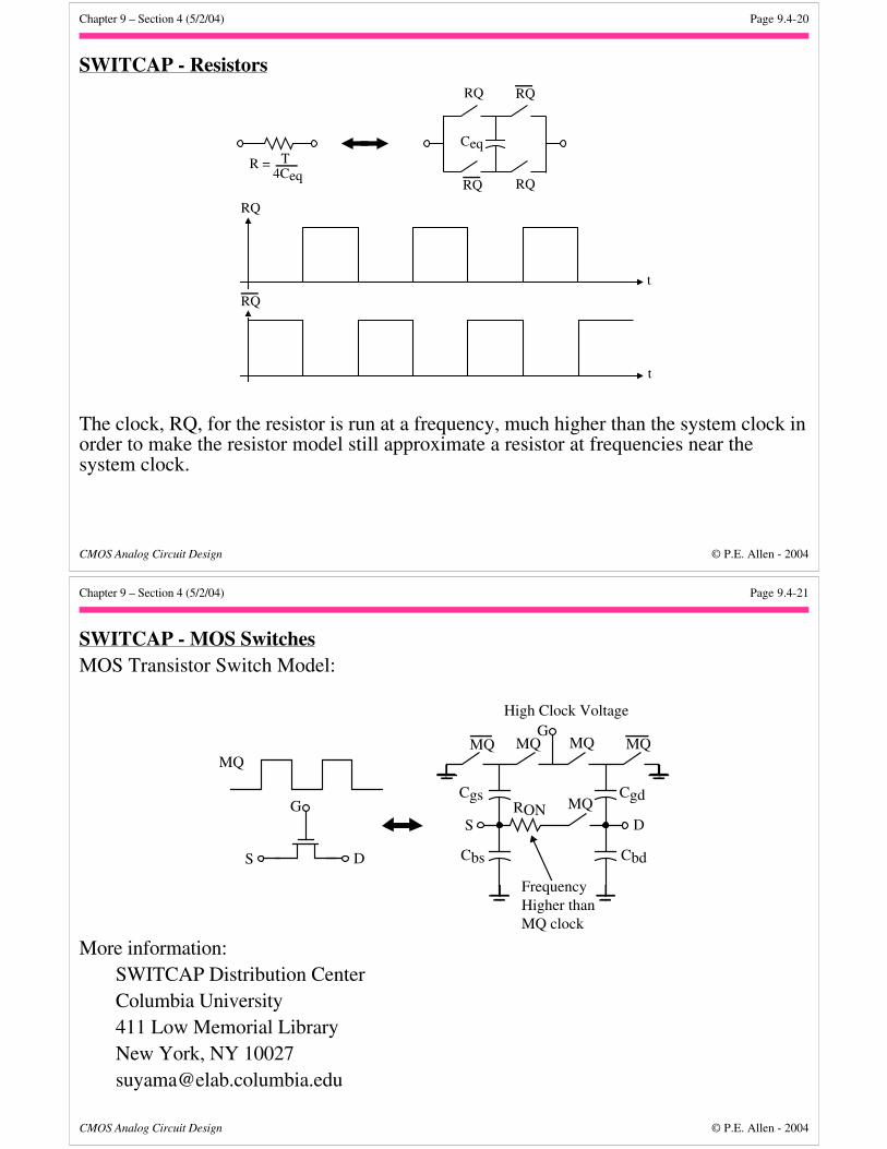
SWITCAP - ResistorsRQ RQ
RQRQ
Ceq
R = T4Ceq
RQ
RQ
t
t
The clock, RQ, for the resistor is run at a frequency, much higher than the system clock inorder to make the resistor model still approximate a resistor at frequencies near thesystem clock.
Chapter 9 – Section 4 (5/2/04) Page 9.4-21
CMOS Analog Circuit Design © P.E. Allen - 2004
SWITCAP - MOS SwitchesMOS Transistor Switch Model:
High Clock Voltage
MQ MQ
Cgd
D
G
RON
Cbd
Cgs
Cbs
S
MQMQ
MQ
FrequencyHigher thanMQ clock
D
G
S
MQ
More information:SWITCAP Distribution CenterColumbia University411 Low Memorial LibraryNew York, NY [email protected]

Chapter 9 – Section 4 (5/2/04) Page 9.4-22
CMOS Analog Circuit Design © P.E. Allen - 2004
SUMMARY• Can replace various switch-capacitor combinations with a z-domain model• The z-domain model consists of:
- Positive and negative conductances
- Delayed conductances (storistor)
- Controlled sources
- Independent sources• These models permit SPICE simulation of switched capacitor circuits• The type of clock circuits considered here are limited to two-phase clocks
Chapter 9 – Section 5 (5/2/04) Page 9.5-1
CMOS Analog Circuit Design © P.E. Allen - 2004
SECTION 9.5 – FIRST-ORDER SWITCHED CAPACITOR CIRCUITSIntroductionObjective:• Examine first-order SC circuits• Illustrate various design methods of SC circuitsApproach:• Low-pass: Design using oversampled assumption and direct z-domain design• High-pass: Design using oversampled assumption and direct z-domain design• All-pass: Design using oversampled assumption and direct z-domain design
Chapter 9 – Section 5 (5/2/04) Page 9.5-2
CMOS Analog Circuit Design © P.E. Allen - 2004
General, First-Order Transfer FunctionsA general first-order transfer function in the s-domain:
H(s) = sa1 ± a0s + b0
a1 = 0 ⇒ Low pass, a0 = 0 ⇒ High Pass, a0 ≠ 0 and a1 ≠ 0 ⇒ All pass
Note that the zero can be in the RHP or LHP.A general first-order transfer function in the z-domain:
H(z) = zA1 ± A0
z - B0 =
A1 ± A0z-1
1 - B0z-1
Chapter 9 – Section 5 (5/2/04) Page 9.5-3
CMOS Analog Circuit Design © P.E. Allen - 2004
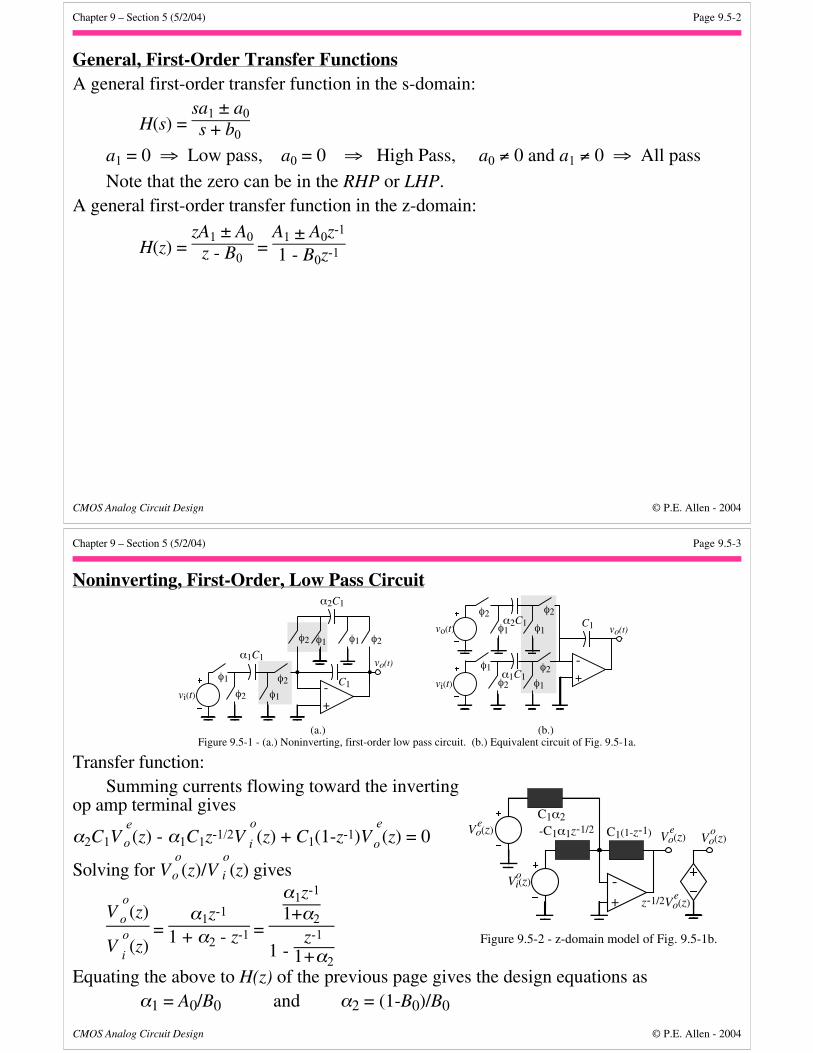
Noninverting, First-Order, Low Pass Circuit
+-
vi(t)
φ1
φ1φ2
φ2
φ2
vo(t)
C1
(a.) (b.)Figure 9.5-1 - (a.) Noninverting, first-order low pass circuit. (b.) Equivalent circuit of Fig. 9.5-1a.
φ1 φ1 φ2
+-
vi(t)
φ1
φ1φ2
φ2
φ2
vo(t)
φ2
φ1φ1vo(t)
α1C1
α2C1
α2C1
α1C1
C1
Transfer function:Summing currents flowing toward the inverting
op amp terminal gives
α2C1V eo (z) - α1C1z-1/2V
oi (z) + C1(1-z-1)V
eo (z) = 0
Solving for V oo (z)/V
oi (z) gives
V oo (z)
V oi(z)
= α1z-1
1 + α2 - z-1 =
α1z-1
1+α2
1 - z-1
1+α2Equating the above to H(z) of the previous page gives the design equations as
α1 = A0/B0 and α2 = (1-B0)/B0
+-Vi(z)
-C1α1z-1/2 C1(1-z-1) Vo(z)e
Vo(z)o
z-1/2Vo(z)e
Vo(z)
C1α2
o
e
Figure 9.5-2 - z-domain model of Fig. 9.5-1b.
Chapter 9 – Section 5 (5/2/04) Page 9.5-4
CMOS Analog Circuit Design © P.E. Allen - 2004
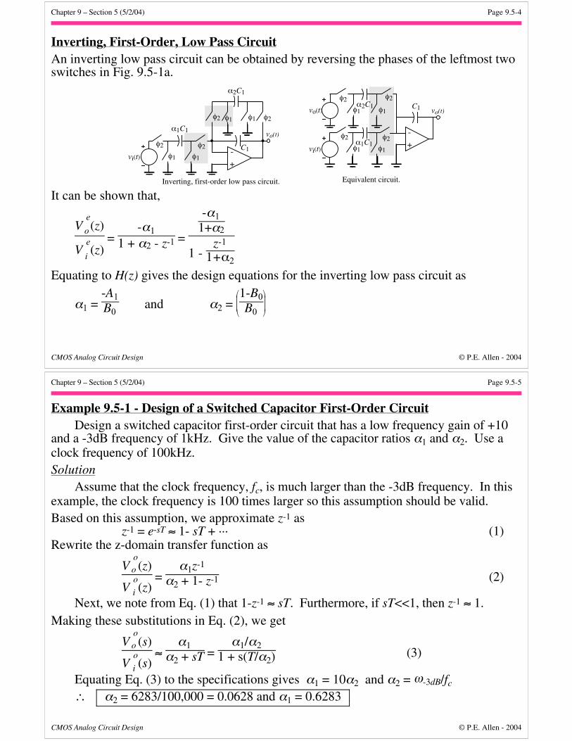
Inverting, First-Order, Low Pass CircuitAn inverting low pass circuit can be obtained by reversing the phases of the leftmost twoswitches in Fig. 9.5-1a.
+-
vi(t)
φ2
φ1φ1
φ2
φ2
vo(t)
C1
Inverting, first-order low pass circuit. Equivalent circuit.
φ1 φ1 φ2
+-
vi(t)
φ2
φ1φ1
φ2
φ2
vo(t)
φ2
φ1φ1vo(t)
α1C1
α2C1
α2C1
α1C1
C1
It can be shown that,
V eo (z)
V ei(z)
= -α1
1 + α2 - z-1 =
-α11+α2
1 - z-1
1+α2
Equating to H(z) gives the design equations for the inverting low pass circuit as
α1 = -A1B0
and α2 =
1-B0
B0
Chapter 9 – Section 5 (5/2/04) Page 9.5-5
CMOS Analog Circuit Design © P.E. Allen - 2004
Example 9.5-1 - Design of a Switched Capacitor First-Order CircuitDesign a switched capacitor first-order circuit that has a low frequency gain of +10
and a -3dB frequency of 1kHz. Give the value of the capacitor ratios α1 and α2. Use aclock frequency of 100kHz.Solution
Assume that the clock frequency, fc, is much larger than the -3dB frequency. In thisexample, the clock frequency is 100 times larger so this assumption should be valid.Based on this assumption, we approximate z-1 as
z-1 = e-sT ≈ 1- sT + ··· (1)Rewrite the z-domain transfer function as
V oo (z)
V oi (z)
= α1z-1
α2 + 1- z-1 (2)
Next, we note from Eq. (1) that 1-z-1 ≈ sT. Furthermore, if sT<<1, then z-1 ≈ 1.Making these substitutions in Eq. (2), we get
V oo (s)
V oi (s)
≈ α1
α2 + sT = α1/α2
1 + s(T/α2) (3)
Equating Eq. (3) to the specifications gives α1 = 10α2 and α2 = ω-3dB/fc∴ α2 = 6283/100,000 = 0.0628 and α1 = 0.6283
Chapter 9 – Section 5 (5/2/04) Page 9.5-6
CMOS Analog Circuit Design © P.E. Allen - 2004
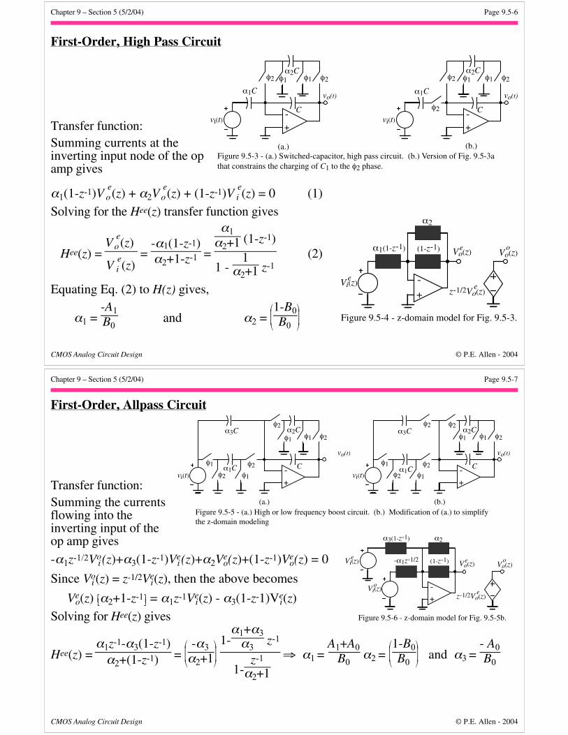
First-Order, High Pass Circuit
Transfer function:Summing currents at theinverting input node of the opamp gives
α1(1-z-1)V eo (z) + α2V
eo (z) + (1-z-1)V
ei (z) = 0 (1)
Solving for the Hee(z) transfer function gives
Hee(z) = V
eo (z)
V ei (z)
= -α1(1-z-1)α2+1-z-1 =
α1α2+1 (1-z-1)
1 - 1
α2+1 z-1 (2)
Equating Eq. (2) to H(z) gives,
α1 = -A1B0
and α2 =
1-B0
B0
+-
vi(t)
φ2
vo(t)α1C
C
φ1 φ1 φ2α2C
+-
vi(t)
φ2
φ2
vo(t)
C
φ1 φ1 φ2
(a.) (b.)Figure 9.5-3 - (a.) Switched-capacitor, high pass circuit. (b.) Version of Fig. 9.5-3athat constrains the charging of C1 to the φ2 phase.
α1C
α2C
+-
Vi(z)
α1(1-z-1) (1-z-1) Vo(z)e
Vo(z)o
z-1/2Vo(z)e
α2
e
Figure 9.5-4 - z-domain model for Fig. 9.5-3.
Chapter 9 – Section 5 (5/2/04) Page 9.5-7
CMOS Analog Circuit Design © P.E. Allen - 2004
First-Order, Allpass Circuit
Transfer function:Summing the currentsflowing into theinverting input of theop amp gives
-α1z-1/2Vo i (z)+α3(1-z-1)Ve
i (z)+α2Ve o(z)+(1-z-1)Ve
o(z) = 0
Since Voi (z) = z-1/2Ve
i(z), then the above becomes
Veo(z) α2+1-z-1 = α1z-1Ve
i(z) - α3(1-z-1)Vei(z)
Solving for Hee(z) gives
Hee(z) = α1z-1-α3(1-z-1)α2+(1-z-1) =
-α3
α2+1 1-α1+α3α3
z-1
1-z-1
α2+1
⇒ α1 = A1+A0
B0 α2 =
1-B0
B0 and α3 =
- A0B0
+-
vi(t)
φ1
φ1φ2
φ2
φ2
vo(t)
C
(b.)
φ1 φ1 φ2
φ2
+-
vi(t)
φ1
φ1φ2
φ2
φ2
vo(t)
α1C C
(a.)
φ1 φ1 φ2α3C
Figure 9.5-5 - (a.) High or low frequency boost circuit. (b.) Modification of (a.) to simplifythe z-domain modeling
α2C α3C α2C
α1C
+-
Vi(z)
-α1z-1/2 (1-z-1) Vo(z)e
Vo(z)o
z-1/2Vo(z)e
α2
o
Figure 9.5-6 - z-domain model for Fig. 9.5-5b.
α3(1-z-1)
Vi(z)e
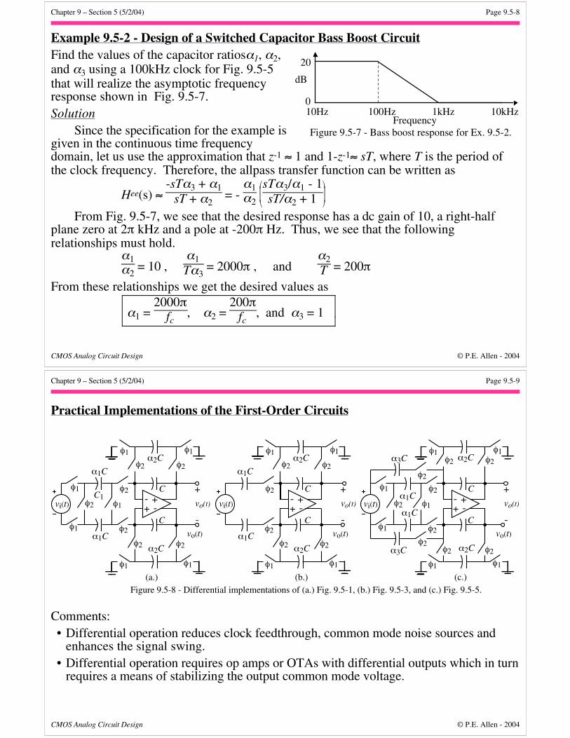
Chapter 9 – Section 5 (5/2/04) Page 9.5-8
CMOS Analog Circuit Design © P.E. Allen - 2004
Example 9.5-2 - Design of a Switched Capacitor Bass Boost CircuitFind the values of the capacitor ratiosα1, α2,and α3 using a 100kHz clock for Fig. 9.5-5that will realize the asymptotic frequencyresponse shown in Fig. 9.5-7.Solution
Since the specification for the example isgiven in the continuous time frequencydomain, let us use the approximation that z-1 ≈ 1 and 1-z-1≈ sT, where T is the period ofthe clock frequency. Therefore, the allpass transfer function can be written as
Hee(s) ≈ -sTα3 + α1
sT + α2 = -
α1α2
sTα3/α1 - 1
sT/α2 + 1
From Fig. 9.5-7, we see that the desired response has a dc gain of 10, a right-halfplane zero at 2π kHz and a pole at -200π Hz. Thus, we see that the followingrelationships must hold.
α1α2
= 10 , α1Tα3
= 2000π , and α2T = 200π
From these relationships we get the desired values as
α1 = 2000π
fc, α2 =
200πfc
, and α3 = 1
dB
20
01kHz 10kHz10Hz 100Hz
FrequencyFigure 9.5-7 - Bass boost response for Ex. 9.5-2.
Chapter 9 – Section 5 (5/2/04) Page 9.5-9
CMOS Analog Circuit Design © P.E. Allen - 2004
Practical Implementations of the First-Order Circuits
+-
vi(t)
φ1
φ1φ2
φ2
φ2
vo(t)C1
C
(a.) (b.)Figure 9.5-8 - Differential implementations of (a.) Fig. 9.5-1, (b.) Fig. 9.5-3, and (c.) Fig. 9.5-5.
φ1 φ1
φ2α2C
vo(t)
+-
C
φ1 φ1
φ2 φ2
φ1 φ2
+
-+-
vi(t)
φ2
φ2
vo(t)
C
φ1 φ1
φ2
vo(t)
+-
C
φ1 φ1
φ2 φ2
φ2
+
-+-
vi(t)
φ1
φ1φ2
φ2
φ2
vo(t)
C
(c.)
φ1 φ1φ2
vo(t)
+-
C
φ1 φ1
φ2 φ2
φ1 φ2
+
-
φ2
φ2α2C
α1C
α1C
α2C
α2C
α1C
α1C
α2C
α2C
α1C
α1C
α3C
α3C
Comments:• Differential operation reduces clock feedthrough, common mode noise sources and
enhances the signal swing.• Differential operation requires op amps or OTAs with differential outputs which in turn
requires a means of stabilizing the output common mode voltage.

Chapter 9 – Section 5 (5/2/04) Page 9.5-10
CMOS Analog Circuit Design © P.E. Allen - 2004
SUMMARY• Examined first-order SC circuits (lowpass, highpass, allpass)• Illustrated design by assuming the clock frequency is higher than the signal frequency
(s-domain design)• Illustrated direct design by equating coefficients between the desired and design in the
z-domain (requires the specifications in the z-domain)
Chapter 9 – Section 6 (5/2/04) Page 9.6-1
CMOS Analog Circuit Design © P.E. Allen - 2004
SECTION 9.6 – SECOND-ORDER SWITCHED CAPACITOR CIRCUITSWhy Second-Order Circuits?
They are fundamental blocks in switched capacitor filters.Switched Capacitor Filter Design Approaches • Cascade design
• Ladder designAlso uses first- and second-order circuits
There are also other applications of first- and second-order circuits:• Oscillators• Converters
First-OrderCircuit
Second-OrderCircuit
Second-OrderCircuit
Second-OrderCircuit
Stage 1 Stage 2 Stage n
Vin Vout
Second-OrderCircuit
Second-OrderCircuit
Stage 1 Stage 2 Stage n
Vin Vout
(a.)
(b.)Figure 9.6-1 - (a.) Cascade design when n is even. (b.) Cascade designwhen n is odd.
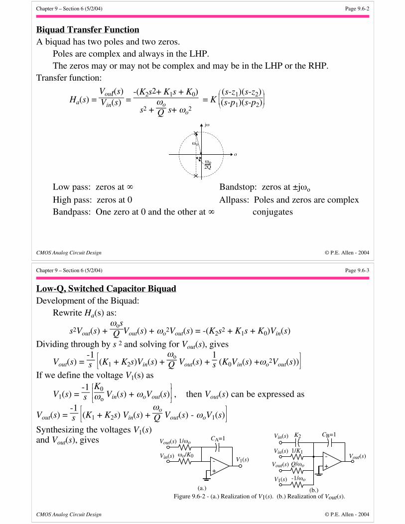
Chapter 9 – Section 6 (5/2/04) Page 9.6-2
CMOS Analog Circuit Design © P.E. Allen - 2004
Biquad Transfer FunctionA biquad has two poles and two zeros.
Poles are complex and always in the LHP.The zeros may or may not be complex and may be in the LHP or the RHP.
Transfer function:
Ha(s) = Vout(s)Vin(s) =
-(K2s2+ K1s + K0)
s2 + ωoQ s+ ωo
2 = K
(s-z1)(s-z2)
(s-p1)(s-p2)
2Qωo
ωo
jω
σ
Low pass: zeros at ∞ Bandstop: zeros at ±jωo
High pass: zeros at 0 Allpass: Poles and zeros are complexBandpass: One zero at 0 and the other at ∞ conjugates
Chapter 9 – Section 6 (5/2/04) Page 9.6-3
CMOS Analog Circuit Design © P.E. Allen - 2004
Low-Q, Switched Capacitor BiquadDevelopment of the Biquad:
Rewrite Ha(s) as:
s2Vout(s) + ωosQ Vout(s) + ωo
2Vout(s) = -(K2s2 + K1s + K0)Vin(s)
Dividing through by s 2 and solving for Vout(s), gives
Vout(s) = -1s
(K1 + K2s)Vin(s) + ωoQ Vout(s) +
1s (K0Vin(s) +ωo
2Vout(s))
If we define the voltage V1(s) as
V1(s) = -1s
K0
ωo Vin(s) + ωoVout(s) , then Vout(s) can be expressed as
Vout(s) = -1s
(K1 + K2s) Vin(s) + ωoQ Vout(s) - ωoV1(s)
Synthesizing the voltages V1(s)and Vout(s), gives
+-
Vout(s)
Vout(s)Vin(s)V1(s)
CA=1
ωo/K0
1/ωo
+-
Vout(s)
Vin(s)
V1(s)
CB=1
Q/ωo
-1/ωo
Vin(s)
1/K1
K2
Figure 9.6-2 - (a.) Realization of V1(s). (b.) Realization of Vout(s).(a.) (b.)
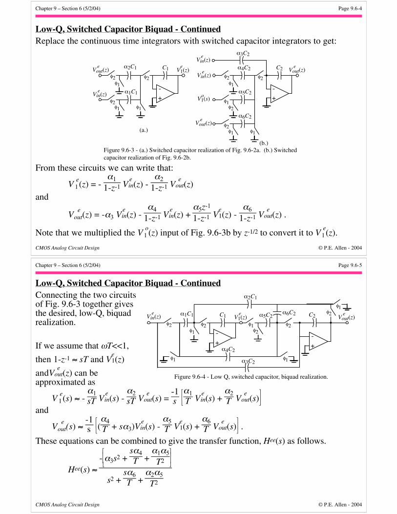
Chapter 9 – Section 6 (5/2/04) Page 9.6-4
CMOS Analog Circuit Design © P.E. Allen - 2004
Low-Q, Switched Capacitor Biquad - ContinuedReplace the continuous time integrators with switched capacitor integrators to get:
+-
Vout(z) V1(z)C1
V1(s)
Figure 9.6-3 - (a.) Switched capacitor realization of Fig. 9.6-2a. (b.) Switchedcapacitor realization of Fig. 9.6-2b.
(a.)
(b.)
Vin(z)
e
e
φ1
φ1 φ1
φ2φ2
α1C1
α2C1
φ2
+-
Vout(z)
C2Vin(z)
e
e
φ1
φ2
φ1
φ2φ2
α5C2
α4C2
φ1
Vin(z)
φ1
α6C2
φ2
o
Vout(z)e
α3C2
e
e
From these circuits we can write that:
V e1(z) = -
α1
1-z-1 Vein(z) -
α2
1-z-1 Ve
out(z)
and
V eout(z) = -α3 V
ein(z) -
α4
1-z-1 Vein(z) +
α5z-1
1-z-1 Ve1(z) -
α6
1-z-1 Ve
out(z) .
Note that we multiplied the V o1 (z) input of Fig. 9.6-3b by z-1/2 to convert it to V
e1(z).
Chapter 9 – Section 6 (5/2/04) Page 9.6-5
CMOS Analog Circuit Design © P.E. Allen - 2004
Low-Q, Switched Capacitor Biquad - ContinuedConnecting the two circuitsof Fig. 9.6-3 together givesthe desired, low-Q, biquadrealization.
If we assume that ωT<<1,
then 1-z-1 ≈ sT and Ve1(z)
andVe
out(z) can beapproximated as
V e1(s) ≈ -
α1sT V
ein(s) -
α2sT V
eout(s) =
-1s
α1
T Vein(s) +
α2T V
eout(s)
and
V eout(s) ≈
-1s
(α4T + sα3)V
ein(s) -
α5T V
e1(s) +
α6T V
eout(s) .
These equations can be combined to give the transfer function, Hee(s) as follows.
Hee(s) ≈ -
α3s2 + sα4T +
α1α5
T2
s2 + sα6T +
α2α5
T2
+-
V1(z)C1
Figure 9.6-4 - Low Q, switched capacitor, biquad realization.
Vin(z)e
φ1
φ1
φ1
φ2φ2
α2C1
α1C1φ2
+-
C2
φ2
α6C2
α4C2
φ2
α5C2
φ1
Vout(z)e
α3C2
e
φ1
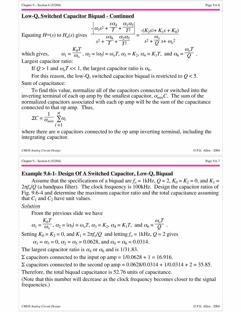
Chapter 9 – Section 6 (5/2/04) Page 9.6-6
CMOS Analog Circuit Design © P.E. Allen - 2004
Low-Q, Switched Capacitor Biquad - Continued
Equating Hee(s) to Ha(s) gives-
α3s2 + sα4T +
α1α5
T2
s2 + sα6T +
α2α5
T2
= -(K2s2+ K1s + K0)
s2 + ωoQ s+ ωo
2
which gives, α1 = K0Tωo
, α2 = |α5| = ωoT, α3 = K2, α4 = K1T, and α6 = ωoTQ .
Largest capacitor ratio:If Q > 1 and ωoT << 1, the largest capacitor ratio is α6.
For this reason, the low-Q, switched capacitor biquad is restricted to Q < 5.Sum of capacitance:
To find this value, normalize all of the capacitors connected or switched into theinverting terminal of each op amp by the smallest capacitor, αminC. The sum of thenormalized capacitors associated with each op amp will be the sum of the capacitanceconnected to that op amp. Thus,
ΣC = 1
αmin ∑i =1
nαi
where there are n capacitors connected to the op amp inverting terminal, including theintegrating capacitor.
Chapter 9 – Section 6 (5/2/04) Page 9.6-7
CMOS Analog Circuit Design © P.E. Allen - 2004
Example 9.6-1- Design Of A Switched Capacitor, Low-Q, BiquadAssume that the specifications of a biquad are fo = 1kHz, Q = 2, K0 = K2 = 0, and K1 =
2πfo/Q (a bandpass filter). The clock frequency is 100kHz. Design the capacitor ratios ofFig. 9.6-4 and determine the maximum capacitor ratio and the total capacitance assumingthat C1 and C2 have unit values.
SolutionFrom the previous slide we have
α1 = K0Tωo
, α2 = |α5| = ωoT, α3 = K2, α4 = K1T, and α6 = ωoTQ .
Setting K0 = K2 = 0, and K1 = 2πfo/Q and letting fo = 1kHz, Q = 2 gives
α1 = α3 = 0, α2 = α5 = 0.0628, and α4 = α6 = 0.0314.
The largest capacitor ratio is α4 or α6 and is 1/31.83.
Σ capacitors connected to the input op amp = 1/0.0628 + 1 = 16.916.Σ capacitors connected to the second op amp = 0.0628/0.0314 + 1/0.0314 + 2 = 35.85.Therefore, the total biquad capacitance is 52.76 units of capacitance.(Note that this number will decrease as the clock frequency becomes closer to the signalfrequencies.)
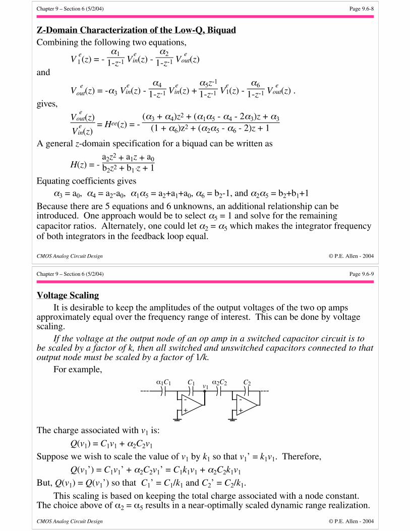
Chapter 9 – Section 6 (5/2/04) Page 9.6-8
CMOS Analog Circuit Design © P.E. Allen - 2004
Z-Domain Characterization of the Low-Q, BiquadCombining the following two equations,
V e1(z) = -
α1
1-z-1 Vein(z) -
α2
1-z-1 Ve
out(z)
and
V eout(z) = -α3 V
ein(z) -
α4
1-z-1 Vein(z) +
α5z-1
1-z-1 Ve1(z) -
α6
1-z-1 Ve
out(z) .
gives,
Ve
out(z)
Vein(z)
= Hee(z) = - (α3 + α4)z2 + (α1α5 - α4 - 2α3)z + α3
(1 + α6)z2 + (α2α5 - α6 - 2)z + 1
A general z-domain specification for a biquad can be written as
H(z) = - a2z2 + a1z + a0
b2z2 + b1˚z + 1
Equating coefficients givesα3 = a0, α4 = a2-a0, α1α5 = a2+a1+a0, α6 = b2-1, and α2α5 = b2+b1+1
Because there are 5 equations and 6 unknowns, an additional relationship can beintroduced. One approach would be to select α5 = 1 and solve for the remainingcapacitor ratios. Alternately, one could let α2 = α5 which makes the integrator frequencyof both integrators in the feedback loop equal.
Chapter 9 – Section 6 (5/2/04) Page 9.6-9
CMOS Analog Circuit Design © P.E. Allen - 2004
Voltage ScalingIt is desirable to keep the amplitudes of the output voltages of the two op amps
approximately equal over the frequency range of interest. This can be done by voltagescaling.
If the voltage at the output node of an op amp in a switched capacitor circuit is tobe scaled by a factor of k, then all switched and unswitched capacitors connected to thatoutput node must be scaled by a factor of 1/k.
For example,
+-
+-
α1C1 C1 α2C2 C2v1
The charge associated with v1 is:
Q(v1) = C1v1 + α2C2v1
Suppose we wish to scale the value of v1 by k1 so that v1’ = k1v1. Therefore,
Q(v1’) = C1v1’ + α2C2v1’ = C1k1v1 + α2C2k1v1
But, Q(v1) = Q(v1’) so that C1’ = C1/k1 and C2’ = C2/k1.
This scaling is based on keeping the total charge associated with a node constant.The choice above of α2 = α5 results in a near-optimally scaled dynamic range realization.
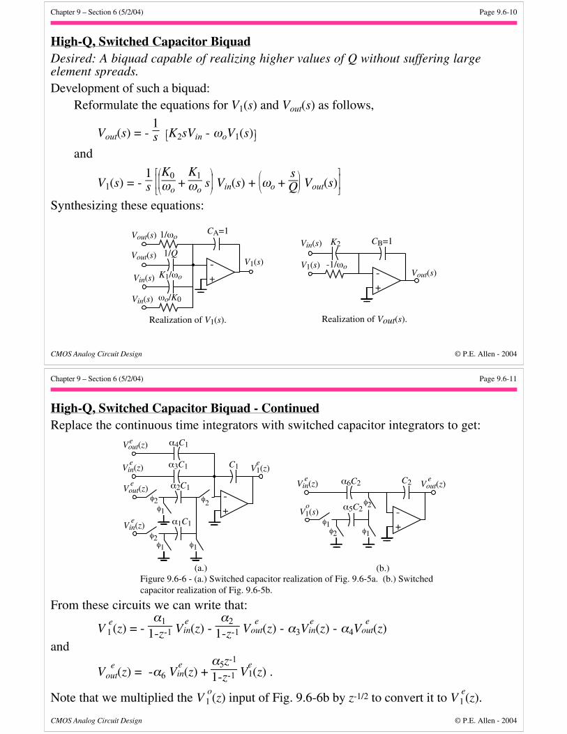
Chapter 9 – Section 6 (5/2/04) Page 9.6-10
CMOS Analog Circuit Design © P.E. Allen - 2004
High-Q, Switched Capacitor BiquadDesired: A biquad capable of realizing higher values of Q without suffering largeelement spreads.Development of such a biquad:
Reformulate the equations for V1(s) and Vout(s) as follows,
Vout(s) = - 1s K2sVin - ωoV1(s)
and
V1(s) = - 1s
K0
ωo +
K1ωo
s Vin(s) +
ωo + sQ Vout(s)
Synthesizing these equations:
+-
Vout(s)
Vout(s)
Vin(s)
V1(s)
CA=1
ωo/K0
1/ωo
+-
Vout(s)
Vin(s)
V1(s)
CB=1
K1/ωo
-1/ωo
Vin(s)1/Q
K2
Realization of V1(s). Realization of Vout(s).
Chapter 9 – Section 6 (5/2/04) Page 9.6-11
CMOS Analog Circuit Design © P.E. Allen - 2004
High-Q, Switched Capacitor Biquad - ContinuedReplace the continuous time integrators with switched capacitor integrators to get:
+-
V1(z)C1
V1(s)
Figure 9.6-6 - (a.) Switched capacitor realization of Fig. 9.6-5a. (b.) Switchedcapacitor realization of Fig. 9.6-5b.
(a.) (b.)
Vin(z)
Vout(z)e
e
φ1
φ1 φ1
φ2φ2
α1C1
α2C1
φ2
+-
Vout(z)
C2Vin(z)
e
e
φ1
φ2α5C2
φ2
α6C2
φ1
o
Vout(z)e
α4C1
eα3C1Vin(z)e
From these circuits we can write that:
V e1(z) = -
α1
1-z-1 Vein(z) -
α2
1-z-1 Ve
out(z) - α3Vein(z) - α4V
eout(z)
and
V eout(z) = -α6 V
ein(z) +
α5z-1
1-z-1 Ve1(z) .
Note that we multiplied the V o1 (z) input of Fig. 9.6-6b by z-1/2 to convert it to V
e1(z).
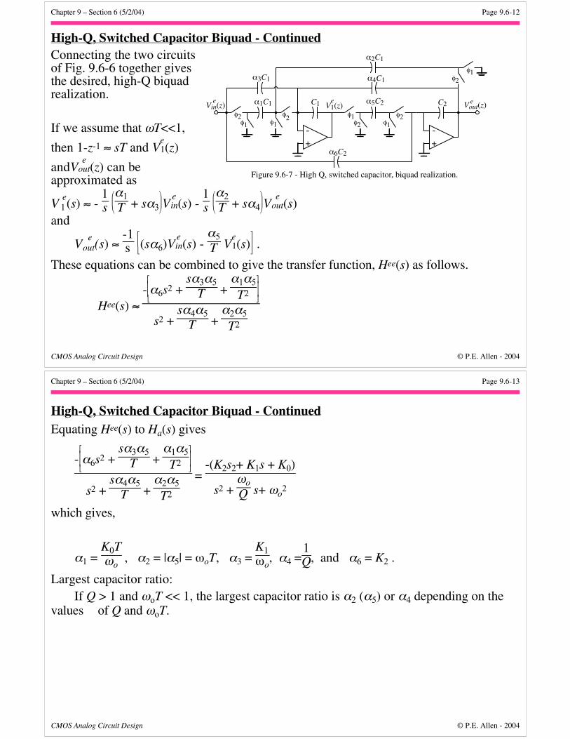
Chapter 9 – Section 6 (5/2/04) Page 9.6-12
CMOS Analog Circuit Design © P.E. Allen - 2004
High-Q, Switched Capacitor Biquad - ContinuedConnecting the two circuitsof Fig. 9.6-6 together givesthe desired, high-Q biquadrealization.
If we assume that ωT<<1,
then 1-z-1 ≈ sT and Ve1(z)
andVe
out(z) can beapproximated as
V e1(s) ≈ -
1s
α1
T + sα3 Vein(s) -
1s
α2
T + sα4 Ve
out(s)and
V eout(s) ≈
-1s
(sα6)Vein(s) -
α5T V
e1(s) .
These equations can be combined to give the transfer function, Hee(s) as follows.
Hee(s) ≈ -
α6s2 + sα3α5
T + α1α5
T2
s2 + sα4α5
T + α2α5
T2
+-
V1(z)C1Vin(z)e
φ1 φ1
φ2
α1C1
α2C1
φ2
+-
C2
φ1
φ2
α5C2
φ2
α6C2
φ1
Vout(z)e
α4C1
e
α3C1
Figure 9.6-7 - High Q, switched capacitor, biquad realization.
φ1φ2
Chapter 9 – Section 6 (5/2/04) Page 9.6-13
CMOS Analog Circuit Design © P.E. Allen - 2004
High-Q, Switched Capacitor Biquad - ContinuedEquating Hee(s) to Ha(s) gives
-
α6s2 + sα3α5
T + α1α5
T2
s2 + sα4α5
T + α2α5
T2
= -(K2s2+ K1s + K0)
s2 + ωoQ s+ ωo
2
which gives,
α1 = K0Tωo
, α2 = |α5| = ωoT, α3 = K1ωo
, α4 =1Q, and α6 = K2 .
Largest capacitor ratio:If Q > 1 and ωoT << 1, the largest capacitor ratio is α2 (α5) or α4 depending on the
values of Q and ωoT.
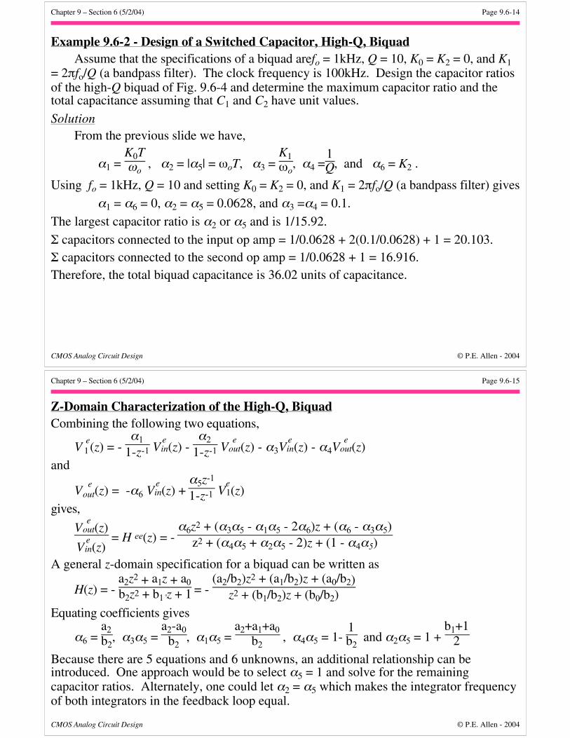
Chapter 9 – Section 6 (5/2/04) Page 9.6-14
CMOS Analog Circuit Design © P.E. Allen - 2004
Example 9.6-2 - Design of a Switched Capacitor, High-Q, BiquadAssume that the specifications of a biquad arefo = 1kHz, Q = 10, K0 = K2 = 0, and K1
= 2πfo/Q (a bandpass filter). The clock frequency is 100kHz. Design the capacitor ratiosof the high-Q biquad of Fig. 9.6-4 and determine the maximum capacitor ratio and thetotal capacitance assuming that C1 and C2 have unit values.
SolutionFrom the previous slide we have,
α1 = K0Tωo
, α2 = |α5| = ωoT, α3 = K1ωo
, α4 =1Q, and α6 = K2 .
Using fo = 1kHz, Q = 10 and setting K0 = K2 = 0, and K1 = 2πfo/Q (a bandpass filter) gives
α1 = α6 = 0, α2 = α5 = 0.0628, and α3 =α4 = 0.1.
The largest capacitor ratio is α2 or α5 and is 1/15.92.
Σ capacitors connected to the input op amp = 1/0.0628 + 2(0.1/0.0628) + 1 = 20.103.Σ capacitors connected to the second op amp = 1/0.0628 + 1 = 16.916.Therefore, the total biquad capacitance is 36.02 units of capacitance.
Chapter 9 – Section 6 (5/2/04) Page 9.6-15
CMOS Analog Circuit Design © P.E. Allen - 2004
Z-Domain Characterization of the High-Q, BiquadCombining the following two equations,
V e1(z) = -
α1
1-z-1 Vein(z) -
α2
1-z-1 Ve
out(z) - α3Vein(z) - α4V
eout(z)
and
V eout(z) = -α6 V
ein(z) +
α5z-1
1-z-1 Ve1(z)
gives,
Ve
out(z)
Vein(z)
= H ee(z) = - α6z2 + (α3α5 - α1α5 - 2α6)z + (α6 - α3α5)
z2 + (α4α5 + α2α5 - 2)z + (1 - α4α5)
A general z-domain specification for a biquad can be written as
H(z) = - a2z2 + a1z + a0
b2z2 + b1˚z + 1 = - (a2/b2)z2 + (a1/b2)z + (a0/b2)
z2 + (b1/b2)z + (b0/b2)
Equating coefficients gives
α6 = a2b2
, α3α5 = a2-a0
b2, α1α5 =
a2+a1+a0b2
, α4α5 = 1- 1b2
and α2α5 = 1 + b1+1
2
Because there are 5 equations and 6 unknowns, an additional relationship can beintroduced. One approach would be to select α5 = 1 and solve for the remainingcapacitor ratios. Alternately, one could let α2 = α5 which makes the integrator frequencyof both integrators in the feedback loop equal.
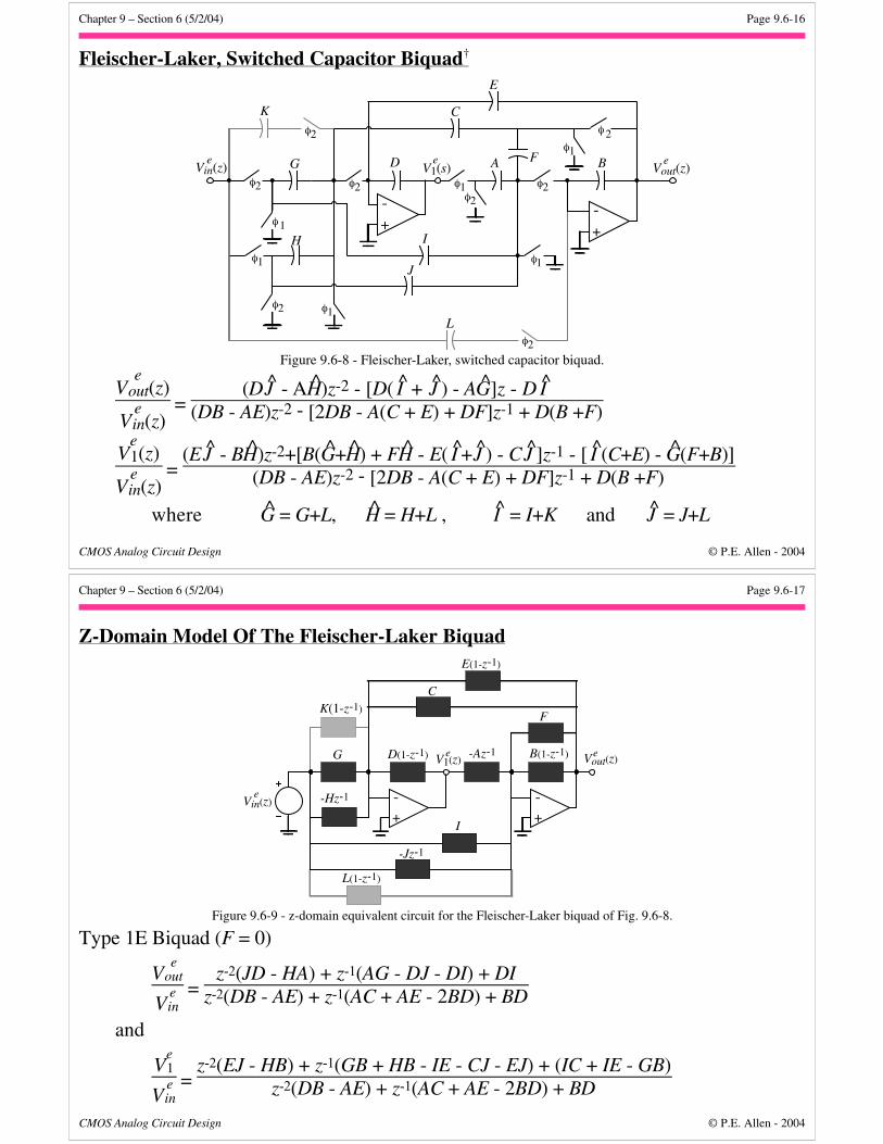
Chapter 9 – Section 6 (5/2/04) Page 9.6-16
CMOS Analog Circuit Design © P.E. Allen - 2004
Fleischer-Laker, Switched Capacitor Biquad†
+-
V1(s)D
Figure 9.6-8 - Fleischer-Laker, switched capacitor biquad.
Vin(z)e
φ1
φ2
φ1
φ2φ2
C
G
φ2
+-
B
φ2
F
I
φ2
A
φ1
Vout(z)ee
φ1φ1
φ2
J
H
L
K
φ1
E
φ2
Ve
out(z)
Vein(z)
= (DJ ^ - AH ^)z-2 - [D( I ^ + J ^) - AG ^]z - D I ^
(DB - AE)z-2 - [2DB - A(C + E) + DF]z-1 + D(B +F)
Ve1(z)
Vein(z)
= (EJ ^ - BH ^)z-2+[B(G ^+H ^) + FH ^ - E( I ^+J ^) - CJ ^]z-1 - [ I ^(C+E) - G ^(F+B)]
(DB - AE)z-2 - [2DB - A(C + E) + DF]z-1 + D(B +F)
where G ^ = G+L, H ^ = H+L , I ^ = I+K and J ^ = J+L
Chapter 9 – Section 6 (5/2/04) Page 9.6-17
CMOS Analog Circuit Design © P.E. Allen - 2004
Z-Domain Model Of The Fleischer-Laker Biquad
+-
Vin(z)
-Az-1 B(1-z-1) Vout(z)e
F
e
I
E(1-z-1)
+-
G D(1-z-1) V1(z)e
CK(1-z-1)
-Hz-1
-Jz-1
L(1-z-1)
Figure 9.6-9 - z-domain equivalent circuit for the Fleischer-Laker biquad of Fig. 9.6-8.
Type 1E Biquad (F = 0)
Ve
out
Vein
= z-2(JD - HA) + z-1(AG - DJ - DI) + DI
z-2(DB - AE) + z-1(AC + AE - 2BD) + BD
and
Ve1
Vein
= z-2(EJ - HB) + z-1(GB + HB - IE - CJ - EJ) + (IC + IE - GB)
z-2(DB - AE) + z-1(AC + AE - 2BD) + BD
Chapter 9 – Section 6 (5/2/04) Page 9.6-18
CMOS Analog Circuit Design © P.E. Allen - 2004
Z-Domain Model of the Fleischer-Laker Biquad - Continued
+-
Vin(z)
-Az-1 B(1-z-1) Vout(z)e
F
e
I
E(1-z-1)
+-
G D(1-z-1) V1(z)e
CK(1-z-1)
-Hz-1
-Jz-1
L(1-z-1)
Figure 9.6-9 - z-domain equivalent circuit for the Fleischer-Laker biquad of Fig. 9.6-8.
Type 1F Biquad (E = 0)
Ve
out
Vein
= z-2(JD - HA) + z-1(AG - DJ - DI) + DI
z-2DB + z-1(AC - 2BD - DF) + (BD + DF)
and
Ve1
Vein
= -z-2HB + z-1(GB + HB + HF - CJ) + (IC + GF - GB)
z-2DB + z-1(AC - 2BD - DF) + (BD + DF)
Chapter 9 – Section 6 (5/2/04) Page 9.6-19
CMOS Analog Circuit Design © P.E. Allen - 2004
Example 9.6-3 - Design of a Switched Capacitor, Fleischer-Laker BiquadUse the Fleischer-Laker biquad to implement the following z-domain transfer
function which has poles in the z-domain at r = 0.98 and θ = ±6.2°.
H(z) = 0.003z-2 + 0.006z-1 + 0.0030.9604z-2 - 1.9485z-1 + 1
SolutionLet us begin by selecting a Type 1E Fleischer-Laker biquad. Equating the numerator
of Eq. (1) with the numerator of H(z) givesDI = 0.003 AG-DJ-DI = 0.006 → AG-DJ = 0.009 DJ-HA = 0.003
If we arbitrarily choose H = 0, we getDI = 0.003 JD = 0.003 AG = 0.012
Picking D = A = 1 gives I = 0.003, J = 0.003 and G = 0.012. Equating the denominatorterms of Eq. (1) with the denominator of H(z), gives
BD = 1 BD-AE = 0.9604 → AE = 0.0396AC+AE-2BD = -1.9485 → AC+AE = 0.0515 → AC = 0.0119
Because we have selected D = A = 1, we get B = 1, E = 0.0396, and C = 0.0119. If anycapacitor value was negative, the procedure would have to be changed by makingdifferent choices or choosing a different realization such as Type 1F.

Chapter 9 – Section 6 (5/2/04) Page 9.6-20
CMOS Analog Circuit Design © P.E. Allen - 2004
Example 9.6-3 - ContinuedSince each of the alphabetic symbols is a capacitor, the largest capacitor ratio
will be D or A divided by I or J which gives 333. The large capacitor ratio is beingcaused by the term BD = 1. If we switch to the Type 1F, the term BD = 0.9604 will causelarge capacitor ratios. This example is a case where both the E and F capacitors areneeded to maintain a smaller capacitor ratio.
Chapter 9 – Section 6 (5/2/04) Page 9.6-21
CMOS Analog Circuit Design © P.E. Allen - 2004
SUMMARY• The second-order switched capacitor circuit is a very versatile circuit• The second-order switched capacitor circuit will be very useful in filter design• Low-Q biquad is good for Qs up to about 5 before the elements spreads become large• Design methods:
- Assume that fc>>fsig and using continuous time specifications and design
- Direct design – equate the z-domain transfer function to a z-domain specificationand solve for the capacitor ratios
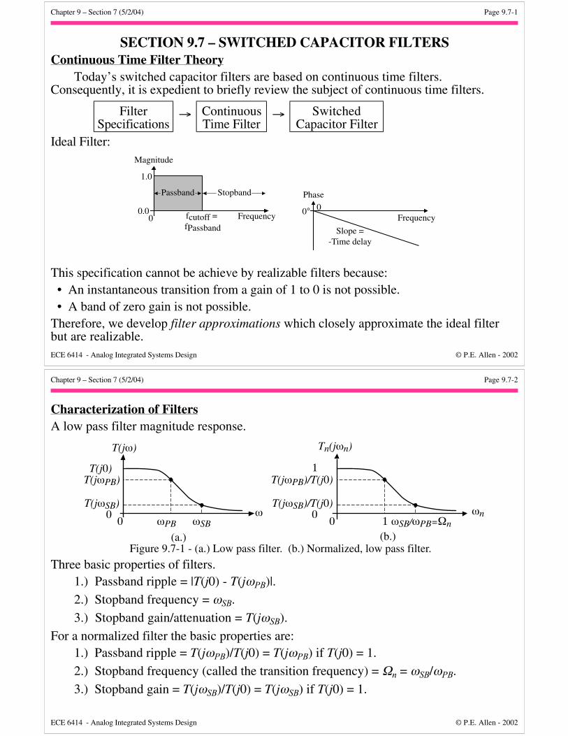
Chapter 9 – Section 7 (5/2/04) Page 9.7-1
ECE 6414 - Analog Integrated Systems Design © P.E. Allen - 2002
SECTION 9.7 – SWITCHED CAPACITOR FILTERSContinuous Time Filter Theory
Today’s switched capacitor filters are based on continuous time filters.Consequently, it is expedient to briefly review the subject of continuous time filters.
FilterSpecifications
→ ContinuousTime Filter
→ SwitchedCapacitor Filter
Ideal Filter:Magnitude
1.0
0.00 fcutoff =
fPassbandFrequency
Passband Stopband Phase
0° 0Frequency
Slope =-Time delay
This specification cannot be achieve by realizable filters because: • An instantaneous transition from a gain of 1 to 0 is not possible. • A band of zero gain is not possible.Therefore, we develop filter approximations which closely approximate the ideal filterbut are realizable.
Chapter 9 – Section 7 (5/2/04) Page 9.7-2
ECE 6414 - Analog Integrated Systems Design © P.E. Allen - 2002
Characterization of FiltersA low pass filter magnitude response.
T(jω)
T(j0)T(jωPB)
T(jωSB)
ωSBωPB0
0ω
T(jωPB)/T(j0)
T(jωSB)/T(j0)
ωSB/ωPB=Ωn
1
0
Tn(jωn)
1ωn0
(a.) (b.)Figure 9.7-1 - (a.) Low pass filter. (b.) Normalized, low pass filter.
Three basic properties of filters.1.) Passband ripple = |T(j0) - T(jωPB)|.
2.) Stopband frequency = ωSB.
3.) Stopband gain/attenuation = T(jωSB).
For a normalized filter the basic properties are:1.) Passband ripple = T(jωPB)/T(j0) = T(jωPB) if T(j0) = 1.
2.) Stopband frequency (called the transition frequency) = Ωn = ωSB/ωPB.
3.) Stopband gain = T(jωSB)/T(j0) = T(jωSB) if T(j0) = 1.

Chapter 9 – Section 7 (5/2/04) Page 9.7-3
ECE 6414 - Analog Integrated Systems Design © P.E. Allen - 2002
Filter Specifications in Terms of Bode Plots (dB)
T(jωPB)
T(jωSB)
Ωn10 log10(ωn)
A(jωPB)
A(jωSB)
Ωn0
Tn(jωn) dB
10
(a.) (b.)Figure 9.7-2 - (a.) Low pass filter of Fig. 9.7-1 as a Bode plot. (b.) Low pass filter ofFig. 9.7-2a shown in terms of attenuation (A(jω) = 1/T(jω)).
An(jωn) dB
log10(ωn)
Therefore,Passband ripple = T(jωPB) dB
Stopband gain = T(jωSB) dB or Stopband attenuation = A(jωPB)
Transition frequency is still = Ωn = ωSB/ωPB
Chapter 9 – Section 7 (5/2/04) Page 9.7-4
ECE 6414 - Analog Integrated Systems Design © P.E. Allen - 2002
Butterworth Filter ApproximationThis approximation is maximally flatin the passband.
Butterworth MagnitudeApproximation:
TLPn(jωn) =
1
1 + ε2 ω2Nn
where N is the order of theapproximation and ε is defined inthe above plot.The magnitude of the Butterworth filter approximation at ωSB is given as
TLPn
jωSB
ωPB = |TLPn(jΩn)| = TSB = 1
1 + ε2 Ω2Nn
This equation in terms of dB is useful for finding N given the filter specifications.
20 log10(TSB) = TSB (dB) = -10 log10
1 + ε2 Ω
2Nn
Normalized Frequency, ωn
0 0.5 1 1.5 2 2.5 30
0.2
0.4
0.6
0.8
1
A
N=5
N=3N=6
11+ε 2
|T LPn (jω )|n
N=8
N=10
N=4N=2
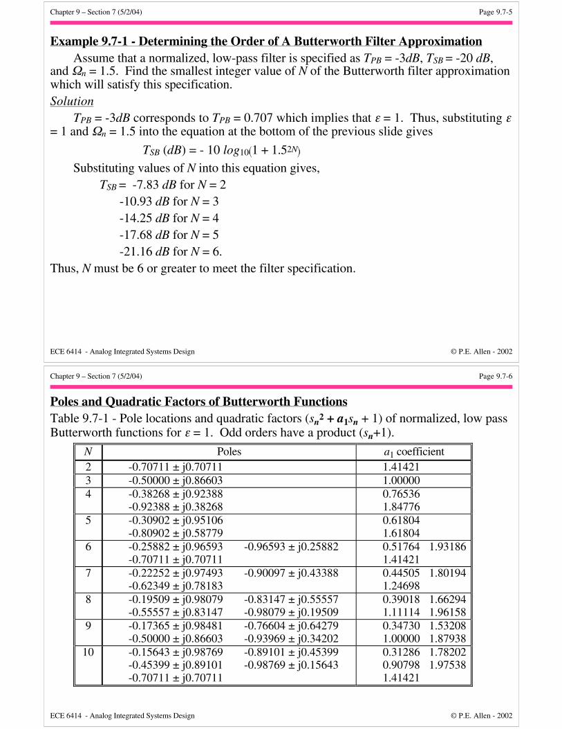
Chapter 9 – Section 7 (5/2/04) Page 9.7-5
ECE 6414 - Analog Integrated Systems Design © P.E. Allen - 2002
Example 9.7-1 - Determining the Order of A Butterworth Filter ApproximationAssume that a normalized, low-pass filter is specified as TPB = -3dB, TSB = -20 dB,
and Ωn = 1.5. Find the smallest integer value of N of the Butterworth filter approximationwhich will satisfy this specification.Solution
TPB = -3dB corresponds to TPB = 0.707 which implies that ε = 1. Thus, substituting ε= 1 and Ωn = 1.5 into the equation at the bottom of the previous slide gives
TSB (dB) = - 10 log10 1 + 1.52N Substituting values of N into this equation gives,
TSB = -7.83 dB for N = 2-10.93 dB for N = 3-14.25 dB for N = 4-17.68 dB for N = 5-21.16 dB for N = 6.
Thus, N must be 6 or greater to meet the filter specification.
Chapter 9 – Section 7 (5/2/04) Page 9.7-6
ECE 6414 - Analog Integrated Systems Design © P.E. Allen - 2002
Poles and Quadratic Factors of Butterworth FunctionsTable 9.7-1 - Pole locations and quadratic factors (sn
2 + a1sn + 1) of normalized, low passButterworth functions for ε = 1. Odd orders have a product (sn+1).
N Poles a1 coefficient2 -0.70711 ± j0.70711 1.414213 -0.50000 ± j0.86603 1.000004 -0.38268 ± j0.92388
-0.92388 ± j0.382680.765361.84776
5 -0.30902 ± j0.95106-0.80902 ± j0.58779
0.618041.61804
6 -0.25882 ± j0.96593 -0.96593 ± j0.25882-0.70711 ± j0.70711
0.51764 1.931861.41421
7 -0.22252 ± j0.97493 -0.90097 ± j0.43388-0.62349 ± j0.78183
0.44505 1.801941.24698
8 -0.19509 ± j0.98079 -0.83147 ± j0.55557-0.55557 ± j0.83147 -0.98079 ± j0.19509
0.39018 1.662941.11114 1.96158
9 -0.17365 ± j0.98481 -0.76604 ± j0.64279-0.50000 ± j0.86603 -0.93969 ± j0.34202
0.34730 1.532081.00000 1.87938
10 -0.15643 ± j0.98769 -0.89101 ± j0.45399-0.45399 ± j0.89101 -0.98769 ± j0.15643-0.70711 ± j0.70711
0.31286 1.782020.90798 1.975381.41421
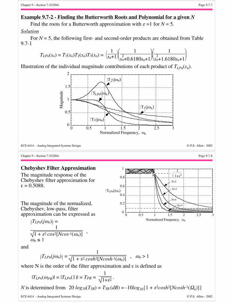
Chapter 9 – Section 7 (5/2/04) Page 9.7-7
ECE 6414 - Analog Integrated Systems Design © P.E. Allen - 2002
Example 9.7-2 - Finding the Butterworth Roots and Polynomial for a given NFind the roots for a Butterworth approximation with ε =1 for N = 5.
SolutionFor N = 5, the following first- and second-order products are obtained from Table
9.7-1
TLPn(sn) = T1(sn)T2(sn)T3(sn) =
1
sn+1
1
s2n+0.6180sn+1
1
s2n+1.6180sn+1
Illustration of the individual magnitude contributions of each product of TLPn(sn).
0
0.5
1
1.5
2
0 0.5 1 1.5 2 2.5 3
T1(jωn)
T2(jωn)
T3(jωn)
(jωnTLPn )
Mag
nitu
de
Normalized Frequency, ωn
Chapter 9 – Section 7 (5/2/04) Page 9.7-8
ECE 6414 - Analog Integrated Systems Design © P.E. Allen - 2002
Chebyshev Filter ApproximationThe magnitude response of theChebyshev filter approximation forε = 0.5088.
The magnitude of the normalized,Chebyshev, low-pass, filterapproximation can be expressed as
TLPn(jωn) =1
1 + ε2 cos2[Ncos-1(ωn)] ,
ωn ≤ 1and
TLPn(jωn) = 1
1 + ε2 cosh2[Ncosh-1(ωn)] , ωn > 1
where N is the order of the filter approximation and ε is defined as
|TLPn(ωPB)| = |TLPn(1)| = TPB = 1
1+ε2 .
N is determined from 20 log10(TSB) = TSB (dB) = -10log101 + ε2cosh2[Ncosh-1(Ωn)]
0
0.2
0.4
0.6
0.8
1
0 0.5 1 1.5 2 2.5 3
TLPn(jωn)
A
N=5
N=2
N=4
N=3
1
1+ε2
Normalized Frequency, ωn
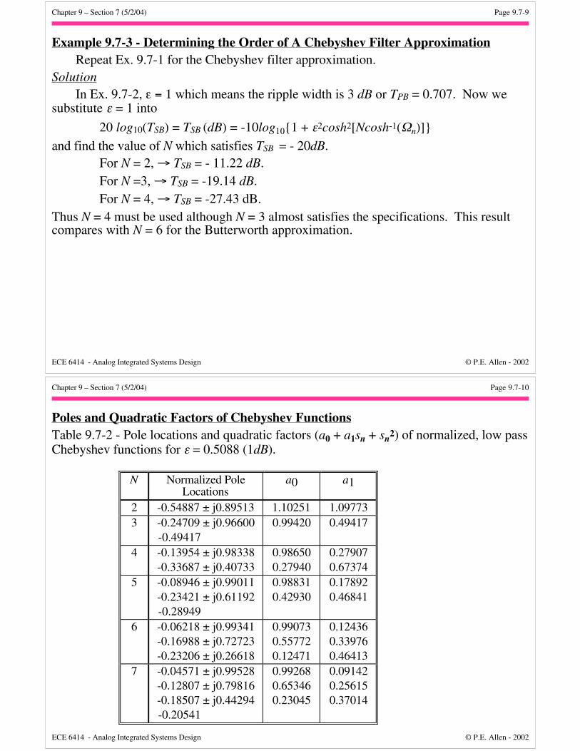
Chapter 9 – Section 7 (5/2/04) Page 9.7-9
ECE 6414 - Analog Integrated Systems Design © P.E. Allen - 2002
Example 9.7-3 - Determining the Order of A Chebyshev Filter ApproximationRepeat Ex. 9.7-1 for the Chebyshev filter approximation.
SolutionIn Ex. 9.7-2, ε = 1 which means the ripple width is 3 dB or TPB = 0.707. Now we
substitute ε = 1 into
20 log10(TSB) = TSB (dB) = -10log101 + ε2cosh2[Ncosh-1(Ωn)]
and find the value of N which satisfies TSB = - 20dB.For N = 2, → TSB = - 11.22 dB.For N =3, → TSB = -19.14 dB.For N = 4, → TSB = -27.43 dB.
Thus N = 4 must be used although N = 3 almost satisfies the specifications. This resultcompares with N = 6 for the Butterworth approximation.
Chapter 9 – Section 7 (5/2/04) Page 9.7-10
ECE 6414 - Analog Integrated Systems Design © P.E. Allen - 2002
Poles and Quadratic Factors of Chebyshev FunctionsTable 9.7-2 - Pole locations and quadratic factors (a0 + a1sn + sn
2) of normalized, low passChebyshev functions for ε = 0.5088 (1dB).
N Normalized PoleLocations
a0 a1
2 -0.54887 ± j0.89513 1.10251 1.097733 -0.24709 ± j0.96600
-0.494170.99420 0.49417
4 -0.13954 ± j0.98338-0.33687 ± j0.40733
0.986500.27940
0.279070.67374
5 -0.08946 ± j0.99011-0.23421 ± j0.61192
-0.28949
0.988310.42930
0.178920.46841
6 -0.06218 ± j0.99341-0.16988 ± j0.72723-0.23206 ± j0.26618
0.990730.557720.12471
0.124360.339760.46413
7 -0.04571 ± j0.99528-0.12807 ± j0.79816-0.18507 ± j0.44294
-0.20541
0.992680.653460.23045
0.091420.256150.37014
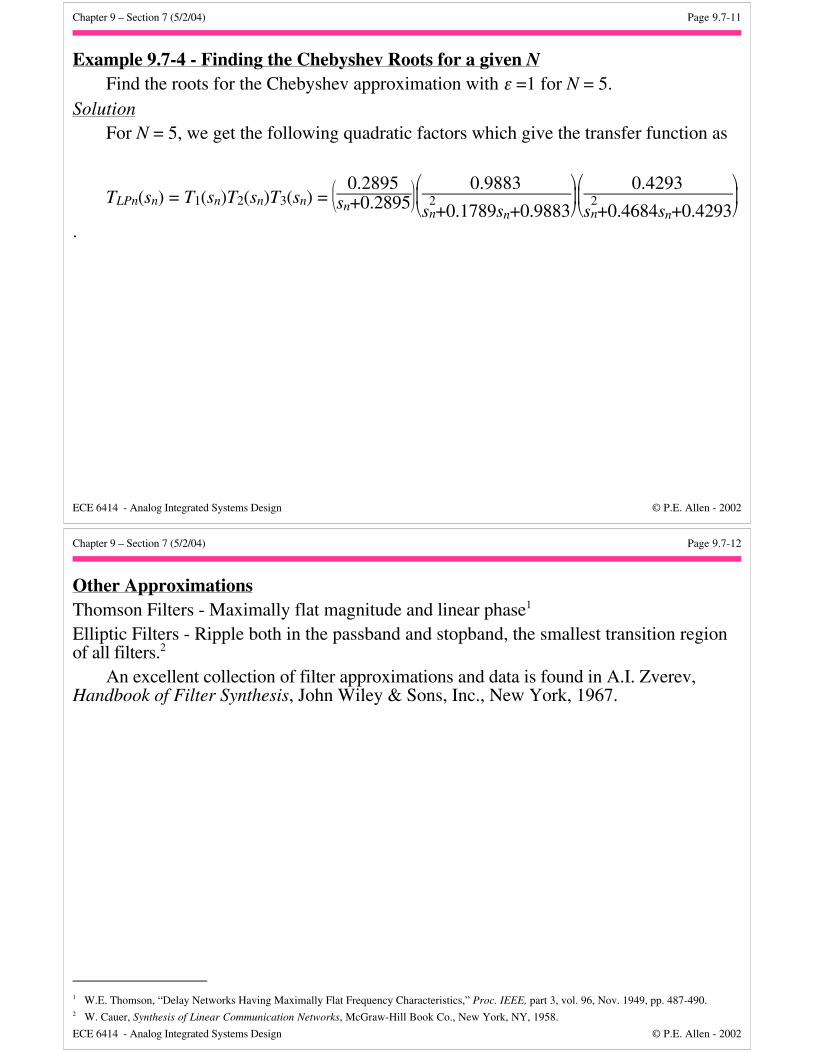
Chapter 9 – Section 7 (5/2/04) Page 9.7-11
ECE 6414 - Analog Integrated Systems Design © P.E. Allen - 2002
Example 9.7-4 - Finding the Chebyshev Roots for a given NFind the roots for the Chebyshev approximation with ε =1 for N = 5.
SolutionFor N = 5, we get the following quadratic factors which give the transfer function as
TLPn(sn) = T1(sn)T2(sn)T3(sn) =
0.2895
sn+0.2895
0.9883
s2n+0.1789sn+0.9883
0.4293
s2n+0.4684sn+0.4293
.
Chapter 9 – Section 7 (5/2/04) Page 9.7-12
ECE 6414 - Analog Integrated Systems Design © P.E. Allen - 2002
Other ApproximationsThomson Filters - Maximally flat magnitude and linear phase1
Elliptic Filters - Ripple both in the passband and stopband, the smallest transition regionof all filters.2
An excellent collection of filter approximations and data is found in A.I. Zverev,Handbook of Filter Synthesis, John Wiley & Sons, Inc., New York, 1967.
1 W.E. Thomson, “Delay Networks Having Maximally Flat Frequency Characteristics,” Proc. IEEE, part 3, vol. 96, Nov. 1949, pp. 487-490.2 W. Cauer, Synthesis of Linear Communication Networks, McGraw-Hill Book Co., New York, NY, 1958.
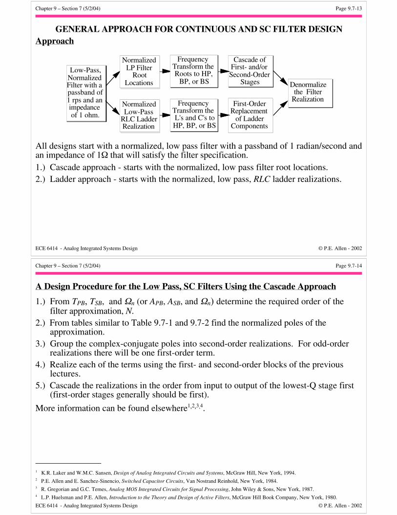
Chapter 9 – Section 7 (5/2/04) Page 9.7-13
ECE 6414 - Analog Integrated Systems Design © P.E. Allen - 2002
GENERAL APPROACH FOR CONTINUOUS AND SC FILTER DESIGNApproach
Low-Pass,NormalizedFilter with a passband of 1 rps and an impedance of 1 ohm.
Denormalize the Filter
Realization
Cascade of First- and/or Second-Order
Stages
First-OrderReplacement
of LadderComponents
Frequency Transform the Roots to HP,
BP, or BS
Frequency Transform the L's and C's to HP, BP, or BS
Normalized LP Filter
RootLocations
Normalized Low-Pass
RLC Ladder Realization
All designs start with a normalized, low pass filter with a passband of 1 radian/second andan impedance of 1Ω that will satisfy the filter specification.1.) Cascade approach - starts with the normalized, low pass filter root locations.2.) Ladder approach - starts with the normalized, low pass, RLC ladder realizations.
Chapter 9 – Section 7 (5/2/04) Page 9.7-14
ECE 6414 - Analog Integrated Systems Design © P.E. Allen - 2002
A Design Procedure for the Low Pass, SC Filters Using the Cascade Approach
1.) From TPB, TSB, and Ωn (or APB, ASB, and Ωn) determine the required order of thefilter approximation, N.
2.) From tables similar to Table 9.7-1 and 9.7-2 find the normalized poles of theapproximation.
3.) Group the complex-conjugate poles into second-order realizations. For odd-orderrealizations there will be one first-order term.
4.) Realize each of the terms using the first- and second-order blocks of the previouslectures.
5.) Cascade the realizations in the order from input to output of the lowest-Q stage first(first-order stages generally should be first).
More information can be found elsewhere1,2,3,4.
1 K.R. Laker and W.M.C. Sansen, Design of Analog Integrated Circuits and Systems, McGraw Hill, New York, 1994.2 P.E. Allen and E. Sanchez-Sinencio, Switched Capacitor Circuits, Van Nostrand Reinhold, New York, 1984.3 R. Gregorian and G.C. Temes, Analog MOS Integrated Circuits for Signal Processing, John Wiley & Sons, New York, 1987.4 L.P. Huelsman and P.E. Allen, Introduction to the Theory and Design of Active Filters, McGraw Hill Book Company, New York, 1980.
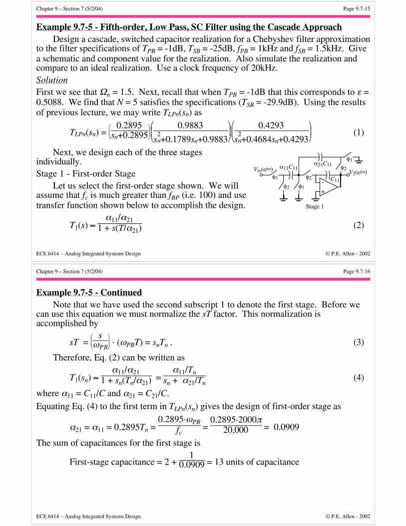
Chapter 9 – Section 7 (5/2/04) Page 9.7-15
ECE 6414 - Analog Integrated Systems Design © P.E. Allen - 2002
Example 9.7-5 - Fifth-order, Low Pass, SC Filter using the Cascade ApproachDesign a cascade, switched capacitor realization for a Chebyshev filter approximation
to the filter specifications of TPB = -1dB, TSB = -25dB, fPB = 1kHz and fSB = 1.5kHz. Givea schematic and component value for the realization. Also simulate the realization andcompare to an ideal realization. Use a clock frequency of 20kHz.SolutionFirst we see that Ωn = 1.5. Next, recall that when TPB = -1dB that this corresponds to ε =0.5088. We find that N = 5 satisfies the specifications (TSB = -29.9dB). Using the resultsof previous lecture, we may write TLPn(sn) as
TLPn(sn) =
0.2895
sn+0.2895
0.9883
s2n+0.1789sn+0.9883
0.4293
s2n+0.4684sn+0.4293
(1)
Next, we design each of the three stagesindividually.Stage 1 - First-order Stage
Let us select the first-order stage shown. We willassume that fc is much greater than fBP (i.e. 100) and usetransfer function shown below to accomplish the design.
T1(s) ≈ α11/α21
1 + s(T/α21) (2)
+-φ1
φ1φ2
φ2
φ2
φ1
α11C11α21C11
C11
Vin(ejω)
Stage 1
V2(ejω)
Chapter 9 – Section 7 (5/2/04) Page 9.7-16
ECE 6414 - Analog Integrated Systems Design © P.E. Allen - 2002
Example 9.7-5 - ContinuedNote that we have used the second subscript 1 to denote the first stage. Before we
can use this equation we must normalize the sT factor. This normalization isaccomplished by
sT =
s
ωPB · (ωPBT) = snTn . (3)
Therefore, Eq. (2) can be written as
T1(sn) ≈ α11/α21
1 + sn(Tn/α21) = α11/Tn
sn + α21/Tn (4)
where α11 = C11/C and α21 = C21/C.
Equating Eq. (4) to the first term in TLPn(sn) gives the design of first-order stage as
α21 = α11 = 0.2895Tn = 0.2895·ωPB
fc =
0.2895·2000π20,000 = 0.0909
The sum of capacitances for the first stage is
First-stage capacitance = 2 + 1
0.0909 = 13 units of capacitance
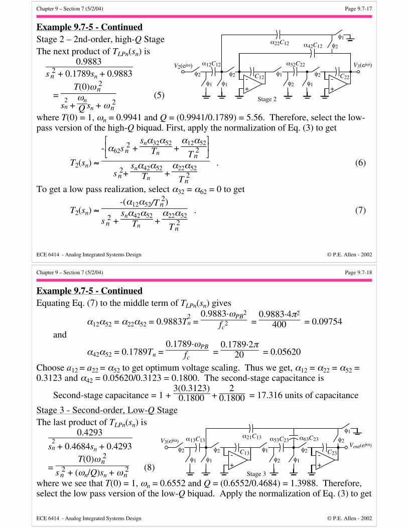
Chapter 9 – Section 7 (5/2/04) Page 9.7-17
ECE 6414 - Analog Integrated Systems Design © P.E. Allen - 2002
Example 9.7-5 - ContinuedStage 2 – 2nd-order, high-Q StageThe next product of TLPn(sn) is
0.9883
s 2n + 0.1789sn + 0.9883
= T(0)ω 2n
s2n +
ωnQ sn + ω 2n
(5)
where T(0) = 1, ωn = 0.9941 and Q = (0.9941/0.1789) = 5.56. Therefore, select the low-pass version of the high-Q biquad. First, apply the normalization of Eq. (3) to get
T2(sn) ≈
-
α62s 2n + snα32α52
Tn +
α12α52
T 2n
s 2n + snα42α52
Tn +
α22α52
T 2n
. (6)
To get a low pass realization, select α32 = α62 = 0 to get
T2(sn) ≈ -(α12α52/T 2n )
s 2n + snα42α52
Tn +
α22α52
T 2n
. (7)
+-φ2
φ1φ1
φ2
α12C12
C12
+-φ1
φ1φ2
φ2
φ2
φ1
α52C22
α22C12
C22
α42C12
V3(ejω)V2(ejω)
Stage 2
Chapter 9 – Section 7 (5/2/04) Page 9.7-18
ECE 6414 - Analog Integrated Systems Design © P.E. Allen - 2002
Example 9.7-5 - ContinuedEquating Eq. (7) to the middle term of TLPn(sn) gives
α12α52 = α22α52 = 0.9883T2n =
0.9883·ωPB2
fc2 =
0.9883·4π2
400 = 0.09754
and
α42α52 = 0.1789Tn = 0.1789·ωPB
fc =
0.1789·2π20 = 0.05620
Choose a12 = a22 = α52 to get optimum voltage scaling. Thus we get, α12 = α22 = α52 =0.3123 and α42 = 0.05620/0.3123 = 0.1800. The second-stage capacitance is
Second-stage capacitance = 1 + 3(0.3123)
0.1800 + 2
0.1800 = 17.316 units of capacitance
Stage 3 - Second-order, Low-Q StageThe last product of TLPn(sn) is
0.4293
s2n + 0.4684sn + 0.4293
= T(0)ω 2n
s 2n + (ωn/Q)sn + ω 2n (8)
where we see that T(0) = 1, ωn = 0.6552 and Q = (0.6552/0.4684) = 1.3988. Therefore,select the low pass version of the low-Q biquad. Apply the normalization of Eq. (3) to get
+-φ2
φ1φ1
φ2
α13C13
C13
+-φ1
φ1φ2
φ2
φ2
φ1
α53C23α21C13
C23
α63C23
Stage 3
V3(ejω)Vout(ejω)
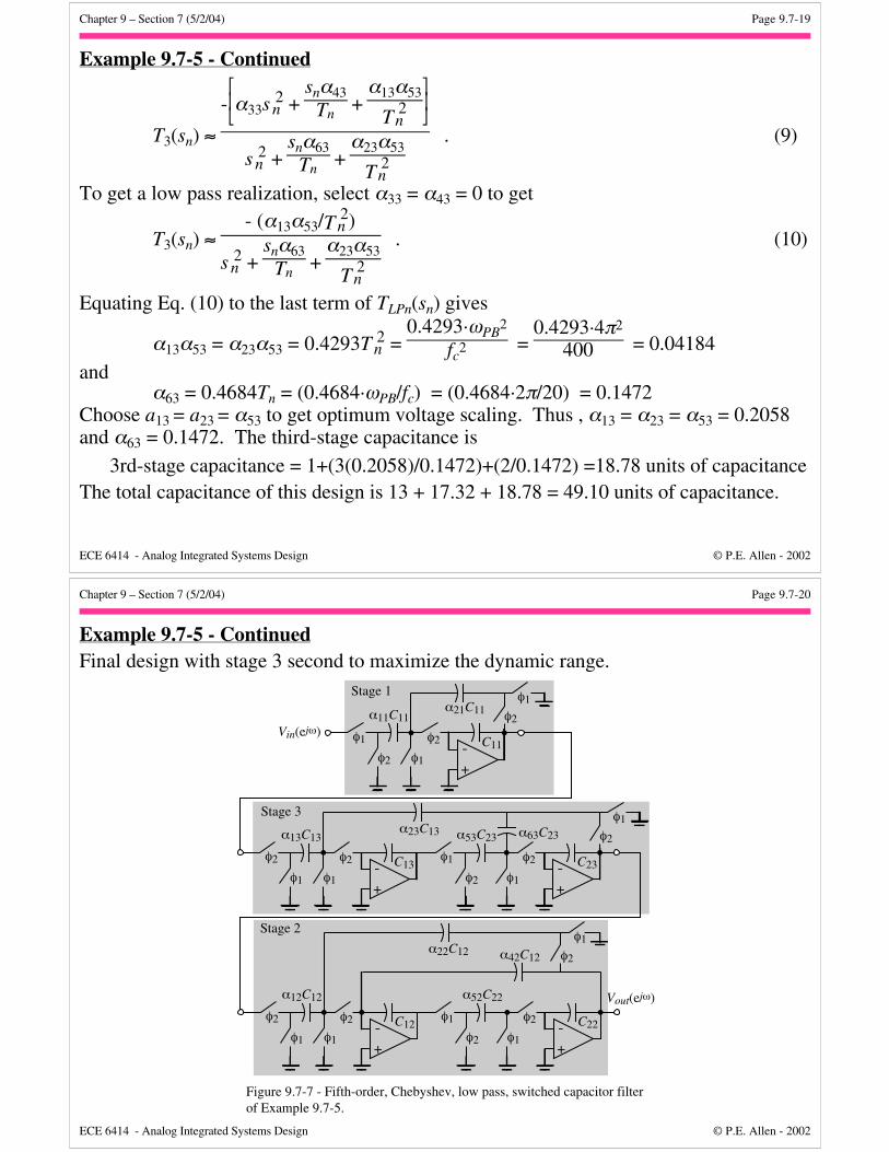
Chapter 9 – Section 7 (5/2/04) Page 9.7-19
ECE 6414 - Analog Integrated Systems Design © P.E. Allen - 2002
Example 9.7-5 - Continued
T3(sn) ≈
-
α33s 2n + snα43
Tn +
α13α53
T 2n
s 2n + snα63
Tn +
α23α53
T 2n
. (9)
To get a low pass realization, select α33 = α43 = 0 to get
T3(sn) ≈ - (α13α53/T 2n )
s 2n + snα63
Tn +
α23α53
T 2n
. (10)
Equating Eq. (10) to the last term of TLPn(sn) gives
α13α53 = α23α53 = 0.4293T 2n = 0.4293·ωPB
2
fc2 =
0.4293·4π2
400 = 0.04184
andα63 = 0.4684Tn = (0.4684·ωPB/fc) = (0.4684·2π/20) = 0.1472
Choose a13 = a23 = α53 to get optimum voltage scaling. Thus , α13 = α23 = α53 = 0.2058and α63 = 0.1472. The third-stage capacitance is
3rd-stage capacitance = 1+(3(0.2058)/0.1472)+(2/0.1472) =18.78 units of capacitanceThe total capacitance of this design is 13 + 17.32 + 18.78 = 49.10 units of capacitance.
Chapter 9 – Section 7 (5/2/04) Page 9.7-20
ECE 6414 - Analog Integrated Systems Design © P.E. Allen - 2002
Example 9.7-5 - ContinuedFinal design with stage 3 second to maximize the dynamic range.
+-φ1
φ1φ2
φ2
φ2
φ1
α11C11α21C11
C11
+-φ2
φ1φ1
φ2
α13C13
C13
+-φ1
φ1φ2
φ2
φ2
φ1
α53C23α23C13
C23
α63C23
+-φ2
φ1φ1
φ2
α12C12
C12
+-φ1
φ1φ2
φ2
φ2
φ1
α52C22
α22C12
C22
α42C12
Vin(ejω)
Vout(ejω)
Stage 1
Stage 3
Stage 2
Figure 9.7-7 - Fifth-order, Chebyshev, low pass, switched capacitor filterof Example 9.7-5.
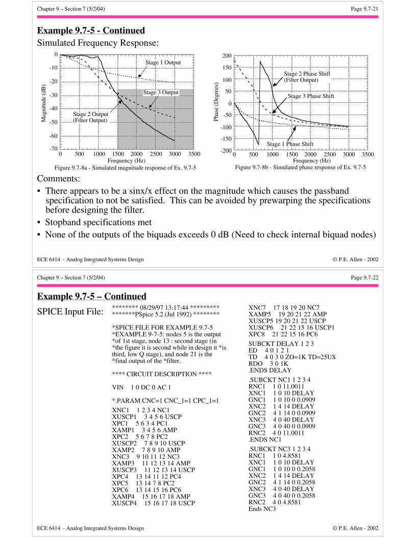
Chapter 9 – Section 7 (5/2/04) Page 9.7-21
ECE 6414 - Analog Integrated Systems Design © P.E. Allen - 2002
Example 9.7-5 - ContinuedSimulated Frequency Response:
-70
-60
-50
-40
-30
-20
-10
0
0 500 1000 1500 2000 2500 3000 3500Frequency (Hz)
Mag
nitu
de (d
B)
Stage 1 Output
Stage 3 Output
Stage 2 Output(Filter Output)
Figure 9.7-8a - Simulated magnitude response of Ex. 9.7-5Frequency (Hz)
-200
-150
-100
-50
0
50
100
150
200
0 500 1000 1500 2000 2500 3000 3500
Phas
e (D
egre
es)
Stage 2 Phase Shift(Filter Output)
Stage 1 Phase Shift
Stage 3 Phase Shift
Figure 9.7-8b - Simulated phase response of Ex. 9.7-5
Comments:• There appears to be a sinx/x effect on the magnitude which causes the passband
specification to not be satisfied. This can be avoided by prewarping the specificationsbefore designing the filter.
• Stopband specifications met• None of the outputs of the biquads exceeds 0 dB (Need to check internal biquad nodes)
Chapter 9 – Section 7 (5/2/04) Page 9.7-22
ECE 6414 - Analog Integrated Systems Design © P.E. Allen - 2002
Example 9.7-5 – Continued
SPICE Input File: ******** 08/29/97 13:17:44 ****************PSpice 5.2 (Jul 1992) ********
*SPICE FILE FOR EXAMPLE 9.7-5*EXAMPLE 9-7-5: nodes 5 is the output*of 1st stage, node 13 : second stage (in*the figure it is second while in design it *isthird, low Q stage), and node 21 is the*final output of the *filter.
**** CIRCUIT DESCRIPTION ****
VIN 1 0 DC 0 AC 1
*.PARAM CNC=1 CNC_1=1 CPC_1=1
XNC1 1 2 3 4 NC1XUSCP1 3 4 5 6 USCPXPC1 5 6 3 4 PC1XAMP1 3 4 5 6 AMPXPC2 5 6 7 8 PC2XUSCP2 7 8 9 10 USCPXAMP2 7 8 9 10 AMPXNC3 9 10 11 12 NC3XAMP3 11 12 13 14 AMPXUSCP3 11 12 13 14 USCPXPC4 13 14 11 12 PC4XPC5 13 14 7 8 PC2XPC6 13 14 15 16 PC6XAMP4 15 16 17 18 AMPXUSCP4 15 16 17 18 USCP
XNC7 17 18 19 20 NC7XAMP5 19 20 21 22 AMPXUSCP5 19 20 21 22 USCPXUSCP6 21 22 15 16 USCP1XPC8 21 22 15 16 PC6
SUBCKT DELAY 1 2 3ED 4 0 1 2 1TD 4 0 3 0 ZO=1K TD=25USRDO 3 0 1K.ENDS DELAY
.SUBCKT NC1 1 2 3 4RNC1 1 0 11.0011XNC1 1 0 10 DELAYGNC1 1 0 10 0 0.0909XNC2 1 4 14 DELAYGNC2 4 1 14 0 0.0909XNC3 4 0 40 DELAYGNC3 4 0 40 0 0.0909RNC2 4 0 11.0011.ENDS NC1
.SUBCKT NC3 1 2 3 4RNC1 1 0 4.8581XNC1 1 0 10 DELAYGNC1 1 0 10 0 0.2058XNC2 1 4 14 DELAYGNC2 4 1 14 0 0.2058XNC3 4 0 40 DELAYGNC3 4 0 40 0 0.2058RNC2 4 0 4.8581Ends NC3
Chapter 9 – Section 7 (5/2/04) Page 9.7-23
ECE 6414 - Analog Integrated Systems Design © P.E. Allen - 2002
Example 9.7-5 - Continued
Spice Input File-Continued
.SUBCKT NC7 1 2 3 4RNC1 1 0 3.2018XNC1 1 0 10 DELAYGNC1 1 0 10 0 0.3123XNC2 1 4 14 DELAYGNC2 4 1 14 0 0.3123XNC3 4 0 40 DELAYGNC3 4 0 40 0 0.3123RNC2 4 0 3.2018.ENDS NC7
.SUBCKT PC1 1 2 3 4RPC1 2 4 11.0011.ENDS PC1
.SUBCKT PC2 1 2 3 4RPC1 2 4 4.8581.ENDS PC2
.SUBCKT PC4 1 2 3 4RPC1 2 4 6.7980.ENDS PC4
.SUBCKT PC6 1 2 3 4RPC1 2 4 3.2018.ENDS PC6
.SUBCKT USCP 1 2 3 4R1 1 3 1R2 2 4 1XUSC1 1 2 12 DELAYGUSC1 1 2 12 0 1XUSC2 1 4 14 DELAY
GUSC2 4 1 14 0 1XUSC3 3 2 32 DELAYGUSC3 2 3 32 0 1XUSC4 3 4 34 DELAYGUSC4 3 4 34 0 1.ENDS USCP
.SUBCKT USCP1 1 2 3 4R1 1 3 5.5586R2 2 4 5.5586XUSC1 1 2 12 DELAYGUSC1 1 2 12 0 0.1799XUSC2 1 4 14 DELAYGUSC2 4 1 14 0 .1799XUSC3 3 2 32 DELAYGUSC3 2 3 32 0 .1799XUSC4 3 4 34 DELAYGUSC4 3 4 34 0 .1799.ENDS USCP1
.SUBCKT AMP 1 2 3 4EODD 3 0 1 0 1E6EVEN 4 0 2 0 1E6.ENDS AMP
.AC LIN 100 10 3K
.PRINT AC V(5) VP(5) V(13)VP(13) V(21) VP(21).PROBE.END
Chapter 9 – Section 7 (5/2/04) Page 9.7-24
ECE 6414 - Analog Integrated Systems Design © P.E. Allen - 2002
Example 9.7-5 - Continued
Spice Input File-Continued
.SUBCKT NC7 1 2 3 4RNC1 1 0 3.2018XNC1 1 0 10 DELAYGNC1 1 0 10 0 0.3123XNC2 1 4 14 DELAYGNC2 4 1 14 0 0.3123XNC3 4 0 40 DELAYGNC3 4 0 40 0 0.3123RNC2 4 0 3.2018.ENDS NC
.SUBCKT PC1 1 2 3 4RPC1 2 4 11.0011.ENDS PC1
.SUBCKT PC2 1 2 3 4RPC1 2 4 4.8581.ENDS PC2
.SUBCKT PC4 1 2 3 4RPC1 2 4 6.7980.ENDS PC4
.SUBCKT PC6 1 2 3 4RPC1 2 4 3.2018.ENDS PC6
.SUBCKT USCP 1 2 3 4R1 1 3 1R2 2 4 1XUSC1 1 2 12 DELAYGUSC1 1 2 12 0 1XUSC2 1 4 14 DELAY
GUSC2 4 1 14 0 1XUSC3 3 2 32 DELAYGUSC3 2 3 32 0 1XUSC4 3 4 34 DELAYGUSC4 3 4 34 0 1.ENDS USCP
.SUBCKT USCP1 1 2 3 4R1 1 3 5.5586R2 2 4 5.5586XUSC1 1 2 12 DELAYGUSC1 1 2 12 0 0.1799XUSC2 1 4 14 DELAYGUSC2 4 1 14 0 .1799XUSC3 3 2 32 DELAYGUSC3 2 3 32 0 .1799XUSC4 3 4 34 DELAYGUSC4 3 4 34 0 .1799.ENDS USCP1
.SUBCKT AMP 1 2 3 4EODD 3 0 1 0 1E6EVEN 4 0 2 0 1E6.ENDS AMP
.AC LIN 100 10 3K
.PRINT AC V(5) VP(5) V(13)VP(13) V(21) VP(21).PROBE.END
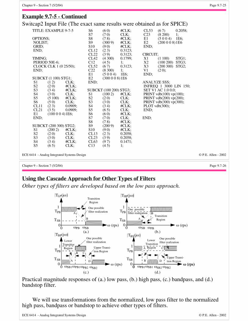
Chapter 9 – Section 7 (5/2/04) Page 9.7-25
ECE 6414 - Analog Integrated Systems Design © P.E. Allen - 2002
Example 9.7-5 - ContinuedSwitcap2 Input File (The exact same results were obtained as for SPICE)
TITLE: EXAMPLE 9-7-5
OPTIONS; NOLIST; GRID; END;
TIMING; PERIOD 50E-6; CLOCK CLK 1 (0 25/50); END;
SUBCKT (1 100) STG1; S1 (1 2) CLK; S2 (2 0) #CLK; S3 (3 4) #CLK; S4 (3 0) CLK; S5 (5 100) #CLK; S6 (5 0) CLK; CL11 (2 3) 0.0909; CL21 (3 5) 0.0909; E1 (100 0 0 4)1E6; END;
SUBCKT (200 300) STG2; S1 (200 2) #CLK; S2 (2 0) CLK; S3 (3 0) CLK; S4 (3 4) #CLK; S5 (6 5) CLK;
S6 (6 0) #CLK; S7 (7 0) CLK; S8 (7 8) #CLK; S9 (300 9) #CLK; S10 (9 0) #CLK; CL12 (2 3) 0.3123; CL22 (3 9) 0.3123; CL42 (4 300) 0.1799; C12 (4 5) 1; CL52 (6 7) 0.3123; C22 (8 300) 1; E1 (5 0 0 4) 1E6; E2 (300 0 0 8)1E6 END;
SUBCKT (100 200) STG3; S1 (100 2) #CLK; S2 (2 0) CLK; S3 (3 0) CLK; S4 (3 4) #CLK; S5 (6 5) CLK; S6 (6 0) #CLK; S7 (7 0) CLK; S8 (7 8) #CLK; S9 (200 9) #CLK; S10 (9 0) #CLK; CL13 (2 3) 0.2058; CL23 (3 9) 0.2058; CL63 (9 7) 0.1471; C13 (4 5) 1;
CL53 (6 7) 0.2058; C23 (8 200) 1; E1 (5 0 0 4) 1E6; E2 (200 0 0 8)1E6 END;
CIRCUIT; X1 (1 100) STG1; X2 (100 200) STG3; X3 (200 300) STG2; V1 (2 0); END;
ANALYZE SSS; INFREQ 1 3000 LIN 150; SET V1 AC 1.0 0.0; PRINT vdb(100) vp(100); PRINT vdb(200) vp(200); PRINT vdb(300) vp(300); PLOT vdb(300); END;
END;
Chapter 9 – Section 7 (5/2/04) Page 9.7-26
ECE 6414 - Analog Integrated Systems Design © P.E. Allen - 2002
Using the Cascade Approach for Other Types of FiltersOther types of filters are developed based on the low pass approach.
(a.) (b.)
(c.) (d.)
0 ωSBωPB
1
0 ω (rps)
TLP(jω)
TPB
TSB
TransitionRegion
A
B
One possiblefilter realization
ωPB
THP(jω)
1
00
ω (rps)
TPB
TSB
ωSB
TransitionRegionA
BOne possiblefilter realization
1
00
ω (rps)
TBP(jω)
ωPB1ωPB2 ωSB2ωSB1
TPB
TSB A
B C
D
One possiblefilter realizationLower
TransitionRegion Upper Transi-
tion Region
0ω (rps)
TBS(jω)
1
00
ω (rps)ωPB1 ωPB2ωSB2ωSB1
TPB
TSB
A
B
C
D
One possiblefilter realization
LowerTransition
Region
Upper Transi-tion Region
Practical magnitude responses of (a.) low pass, (b.) high pass, (c.) bandpass, and (d.)bandstop filter.
We will use transformations from the normalized, low pass filter to the normalizedhigh pass, bandpass or bandstop to achieve other types of filters.
Chapter 9 – Section 7 (5/2/04) Page 9.7-27
ECE 6414 - Analog Integrated Systems Design © P.E. Allen - 2002
High Pass, SC Filters Using the Cascade ApproachNormalized, low pass to normalized high pass transformation:
sln = 1
shn
where shn is the normalized, high-pass frequency variable.A general form of the normalized, low-pass transfer function is
TLPn(sln) = p1lnp2lnp3ln···pNln
(sln+p1ln)(sln+p2ln)(sln+p3ln)···(sln+pNln)
where pkln is the kth normalized, low-pass pole.Applying the normalized, low-pass to high-pass transformation toTLPn(sln) gives
THPn(shn) = p1lnp2lnp3ln···pNln
1
shn+p1ln
1
shn+p2ln
1
shn+p3ln ···
1
shn+pNln
= s
Nhn
shn+1
p1ln
shn+1
p2ln
shn+1
p3ln···
shn+1
pNln
= s
Nhn
shn+p1hn shn+p2hn shn+p3hn ··· shn+pNhn
where pkhn is the kth normalized high-pass pole.Use high pass switched capacitor circuits to achieve the implementation.
Ωn is defined for the high pass normalized filter as: Ωn = 1Ωhn
= ωPBωSB
Chapter 9 – Section 7 (5/2/04) Page 9.7-28
ECE 6414 - Analog Integrated Systems Design © P.E. Allen - 2002
Example 9.7-6 - Design of a Butterworth, High-Pass FilterDesign a high-pass filter having a -3dB ripple bandwidth above 1 kHz and a gain of
less than -35 dB below 500 Hz using the Butterworth approximation. Use a clockfrequency of 100kHz.Solution
From the specification, we know that TPB = -3 dB and TSB = -35 dB. Also, Ωn = 2(Ωhn = 0.5). ε = 1 because TPB = -3 dB. Therefore, find that N = 6 will give TSB = -36.12dB which is the lowest, integer value of N which meets the specifications.
Next, the normalized, low-pass poles are found from Table 9.7-1 asp1ln, p6ln = -0.2588 ± j 0.9659p2ln, p5ln = -0.7071 ± j 0.7071
andp3ln, p4ln = -0.9659 ± j 0.2588
Inverting the normalized, low-pass poles gives the normalized, high-pass poles which are
p1hn, p6hn = -0.2588 -+ j 0.9659
p2hn, p5hn = -0.7071 -+ j 0.7071and
p3hn, p4hn = -0.9659 -+ j 0.2588 .
We note the inversion of the Butterworth poles simply changes the sign of the imaginarypart of the pole.
Chapter 9 – Section 7 (5/2/04) Page 9.7-29
ECE 6414 - Analog Integrated Systems Design © P.E. Allen - 2002
Example 9.7-6 - ContinuedThe next step is to group the poles in second-order products, since there are no first-
order products. This result gives the following normalized, high-pass transfer function.THPn(shn) = T1(shn)T2(shn)T3(shn)
=
s2hn
(shn+p1hn)(shn+p6hn)
s2hn
(shn+p2hn)(shn+p5hn)
s2hn
(shn+p3hn)(shn+p4hn)
=
s
2hn
s2hn+0.5176shn+1
s
2hn
s2hn+1.4141shn+1
s
2hn
s2hn+1.9318shn+1
.
Now we are in a position to do the stage-by-stage design. We see that the Q’s ofeach stage are Q1 = 1/0.5176 = 1.932, Q2 = 1/1.414 = 0.707, and Q3 = 1/1.9318 = 0.5176.Therefore, we will choose the low-Q biquad to implement the realization of this example.The low-Q biquad design equations are:
α1 = (K0Tn/ωon) , α2 = |α5| = ωonTn, α3 = K2, α4 = K1Tn, and α6 = (ωonTn/Q) .For the high pass,
K0=K1=0 and K2=1, so that α1=α4=0 and α2=|α5| = ωonTn, α3 = K2 and α6 = ωonTn
Q .Stage 1
α21=α51=(ωPB/fc)=(2π·103/105)=0.06283, α31 = 1,and α61 = (ωPB/Qfc) = (0.06283/1.932) = 0.03252
Chapter 9 – Section 7 (5/2/04) Page 9.7-30
ECE 6414 - Analog Integrated Systems Design © P.E. Allen - 2002
Example 9.7-6 - ContinuedStage 2
α22 = α52 = ωPBfc
= 2π·103
105 = 0.06283,
α32 = 1, and
α62 = ωPBQfc =
0.062830.707 = 0.08884
Stage 3
α23 = α53 = ωPBfc
= 2π·103
105 = 0.06283,
α33 = 1, and
α63 = ωPBQfc =
0.062830.5176 = 0.1214
Realization →Lowest Q stages are first in the cascade
realization.Σ capacitances = 104.62 units of capacitance
+-
C23Vin(z)e
φ1
φ1
φ2 α23C13
φ2
+-
C13
φ2
α63C23
φ2
α53C23
φ1
V3(z)eα33C23
φ1
φ1φ2
+-
C21 Vout(z)e
φ1
φ1
φ2 α21C11
φ2
+-
C11
φ2
α61C21
φ2
α51C21
φ1
α31C21
φ1
φ1φ2
V2(z)e
φ1φ1
φ2
α21C12 φ2C12
α62C22
φ2
α52C22
α32C22
φ1
φ1
φ2
+-
C22
+-
φ1φ2
Stage 3
Stage 2
Stage 1
Chapter 9 – Section 7 (5/2/04) Page 9.7-31
ECE 6414 - Analog Integrated Systems Design © P.E. Allen - 2002
Bandpass, SC Filters Using the Cascade Approach1.) Define the passband and stopband as
BW = ωPB2 - ωPB1 and SW = ωSB2 - ωSB1where ωPB2 (ωPB1) is the larger (smaller) passband of the bandpass filter. ωSB2 (ωSB1) isthe larger (smaller) stopband frequency.2.) Geometrically centered bandpass filters have the following relationship:
ωr = ωPB1ωPB2 = ωSB2ωSB1 3.) Define a normalized low-pass to unnormalized bandpass transformation as
sln = 1
BW
sb
2 + ωr2
sb =
1BW
sb + ωr
2
sb .
4.) A normalized low-pass to normalized bandpass transformation is achieved bydividing the bandpass variable, sb, by the geometric center frequency, ωr, to get
sln =
ωr
BW
sb
ωr + 1
(sb/ωr) =
ωr
BW
sbn + 1
sbn where sbn =
sbωr .
5.) Multiply by BW/ωr and define yet a further normalization as
sln' =
BW
ωr sln = Ωbsln = Ωb
sl
ωPB =
sbn + 1
sbn where Ωb =
BWωr .
6.) Solve for sbn in terms of sln' from the following quadratic equation.
s2bn - sln' sbn + 1 = 0 → sbn =
sln' /2 ±
sln' /2 2 - 1 .
Chapter 9 – Section 7 (5/2/04) Page 9.7-32
ECE 6414 - Analog Integrated Systems Design © P.E. Allen - 2002
Illustration of the Above Approach
(a.) (b.)
0 ωbn (rps)
1
00
TPBn(jωb)
ωr-ωr
BW BW
ωb (rps)(c.)(d.)
Bandpass Normalization
Normalized low-pass to normalized bandpass
transformation
BandpassDenormalization
1
00-1 1
TLPn(jωln )
ωln (rps)ωrωPB
1
00
1Ωb-Ωb
TLPn(jωln' )
ωln' (rps)
sln'
2 ±
sln'
2
2
- 1
↓sbn
1
0
TBPn(jωbn )
ΩbΩb
1-1
sb ← Ωbsbn = BWωr
sbn
Ωbsln = BWωr
sln → sln'
Figure 9.7-10 - Illustration of the development of a bandpass filter from a low-pass filter.(a.) Ideal normalized, low-pass filter. (b.) Normalization of (a.) for bandpasstransformation. (c.) Application of low-pass to bandpass transformation. (d.)Denormalized bandpass filter.
Chapter 9 – Section 7 (5/2/04) Page 9.7-33
ECE 6414 - Analog Integrated Systems Design © P.E. Allen - 2002
Bandpass Design Procedure for the Cascade Approach1.) The ratio of the stop bandwidth to the pass bandwidth is defined as
Ωn = SWBW =
ωSB2 - ωSB1
ωPB2 - ωPB1.
2.) From TPB, TSB, and Ωn, find the order N or the filter.
3.) Find the normalized, low-pass poles, p‘ kln.
4.) The normalized bandpass poles can be found from the normalized, low pass poles, p‘ kln
using
pkbn = p‘
kln2 ±
p ‘
kln2
2 - 1 .
For each pole of the low-pass filter, two polesresult for the bandpass filter.
Figure 9.7-11 - Illustration of how thenormalized, low-pass, complex conjugatepoles are transformed into two normalized,bandpass, complex conjugate poles.
pjln'
pkln'
= pjln' *
pkbn*
pjbn*
pjbn
pkbn
jωln'
σln' σbn
jωbn
Low-pass PolesNormalized by ωPBωr
BWNormalized
Bandpass Poles
Chapter 9 – Section 7 (5/2/04) Page 9.7-34
ECE 6414 - Analog Integrated Systems Design © P.E. Allen - 2002
Bandpass Design Procedure for the Cascade Approach - Continued5.) Group the poles and zeros into second-order products having the following form
Tk(sbn) = Kk sbn
(sbn + pkbn)(sbn + pjbn* ) =
Kk sbn(sbn+σkbn+jωkbn)(sbn+σkbn-jωkbn)
= Kk sbn
sbn2 +(2σkbn)sbn+(σbn
2 +ωkbn2 ) =
Tk(ωkon)
ωkon
Qksbn
sbn2 +
ωkon
Qksbn + ωkon
2
where j and k corresponds to the jth and kth low-pass poles which are a complexconjugate pair, Kk is a gain constant, and
ωkon = σkbn2 +ωkbn
2 and Qk = σbn
2 +ωkbn2
2σbn .
6.) Realize each second-order product with a bandpass switched capacitor biquad andcascade in the order of increasing Q.
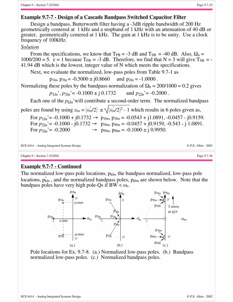
Chapter 9 – Section 7 (5/2/04) Page 9.7-35
ECE 6414 - Analog Integrated Systems Design © P.E. Allen - 2002
Example 9.7-7 - Design of a Cascade Bandpass Switched Capacitor FilterDesign a bandpass, Butterworth filter having a -3dB ripple bandwidth of 200 Hz
geometrically centered at 1 kHz and a stopband of 1 kHz with an attenuation of 40 dB orgreater, geometrically centered at 1 kHz. The gain at 1 kHz is to be unity. Use a clockfrequency of 100kHz.Solution
From the specifications, we know that TPB = -3 dB and TSB = -40 dB. Also, Ωn =1000/200 = 5. ε = 1 because TPB = -3 dB. Therefore, we find that N = 3 will give TSB = -41.94 dB which is the lowest, integer value of N which meets the specifications.
Next, we evaluate the normalized, low-pass poles from Table 9.7-1 asp1ln, p3ln = -0.5000 ± j0.8660 and p2ln = -1.0000 .
Normalizing these poles by the bandpass normalization of Ωb = 200/1000 = 0.2 givesp1ln’, p3ln’= -0.1000 ± j 0.1732 and p2ln’= -0.2000 .
Each one of the pkln’will contribute a second-order term. The normalized bandpass
poles are found by using sbn =
sln' /2 ±
sln' /2 2 - 1 which results in 6 poles given as,
For p1ln’= -0.1000 + j0.1732 → p1bn, p2bn = -0.0543 + j1.0891, -0.0457 - j0.9159.For p2ln’= -0.1000 - j0.1732 → p3bn, p4bn = -0.0457 + j0.9159, -0.543 - j 1.0891.For p3ln’= -0.2000 → p5bn, p6bn = -0.1000 ± j 0.9950.
Chapter 9 – Section 7 (5/2/04) Page 9.7-36
ECE 6414 - Analog Integrated Systems Design © P.E. Allen - 2002
Example 9.7-7 - ContinuedThe normalized low-pass pole locations, pkln, the bandpass normalized, low-pass polelocations, pkln' , and the normalized bandpass poles, pkbn are shown below. Note that thebandpass poles have very high pole-Qs if BW < ωr.
p1ln
p2ln
p3ln
p3ln'
p2ln'p1ln
'
j1
-j1
-1σln
'
jωln'
(b.)(a.)
-1
j1
-j1
-0.5000
j0.8660
-j0.8660
jωln
σln
p1ln
p2ln
p3ln
σbn
p1bn
p2bn
p3bn
p4bn
p5bn
p6bn
jωbn
j1
-1
-j1
(c.)
3 zerosat ±j∞
Pole locations for Ex. 9.7-8. (a.) Normalized low-pass poles. (b.) Bandpassnormalized low-pass poles. (c.) Normalized bandpass poles.
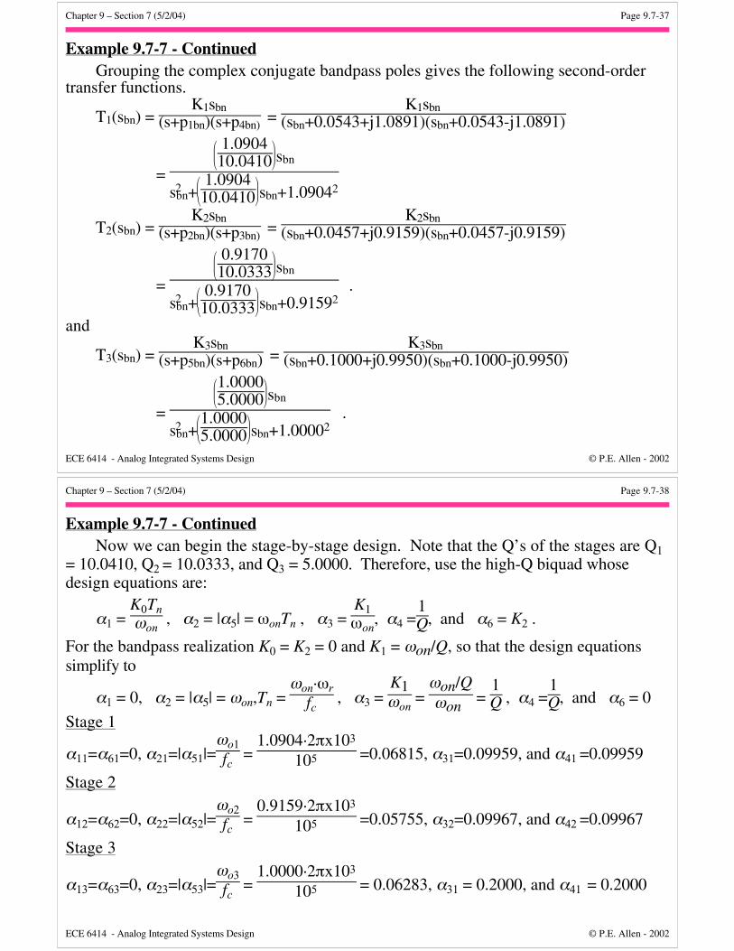
Chapter 9 – Section 7 (5/2/04) Page 9.7-37
ECE 6414 - Analog Integrated Systems Design © P.E. Allen - 2002
Example 9.7-7 - ContinuedGrouping the complex conjugate bandpass poles gives the following second-order
transfer functions.
T1(sbn) = K1sbn
(s+p1bn)(s+p4bn) =
K1sbn(sbn+0.0543+j1.0891)(sbn+0.0543-j1.0891)
=
1.0904
10.0410 sbn
sbn2 +
1.0904
10.0410 sbn+1.09042
T2(sbn) = K2sbn
(s+p2bn)(s+p3bn) =
K2sbn(sbn+0.0457+j0.9159)(sbn+0.0457-j0.9159)
=
0.9170
10.0333 sbn
sbn2 +
0.9170
10.0333 sbn+0.91592 .
and
T3(sbn) = K3sbn
(s+p5bn)(s+p6bn) = K3sbn
(sbn+0.1000+j0.9950)(sbn+0.1000-j0.9950)
=
1.0000
5.0000 sbn
sbn2 +
1.0000
5.0000 sbn+1.00002 .
Chapter 9 – Section 7 (5/2/04) Page 9.7-38
ECE 6414 - Analog Integrated Systems Design © P.E. Allen - 2002
Example 9.7-7 - ContinuedNow we can begin the stage-by-stage design. Note that the Q’s of the stages are Q1
= 10.0410, Q2 = 10.0333, and Q3 = 5.0000. Therefore, use the high-Q biquad whosedesign equations are:
α1 = K0Tnωon
, α2 = |α5| = ωonTn , α3 = K1ωon
, α4 =1Q, and α6 = K2 .
For the bandpass realization K0 = K2 = 0 and K1 = ωon/Q, so that the design equationssimplify to
α1 = 0, α2 = |α5| = ωon,Tn = ωon·ωr
fc , α3 =
K1ωon
= ωon/Qωon =
1Q , α4 =
1Q, and α6 = 0
Stage 1
α11=α61=0, α21=|α51|=ωo1fc
= 1.0904·2πx103
105 =0.06815, α31=0.09959, and α41 =0.09959
Stage 2
α12=α62=0, α22=|α52|=ωo2fc
= 0.9159·2πx103
105 =0.05755, α32=0.09967, and α42 =0.09967
Stage 3
α13=α63=0, α23=|α53|=ωo3fc
= 1.0000·2πx103
105 = 0.06283, α31 = 0.2000, and α41 = 0.2000
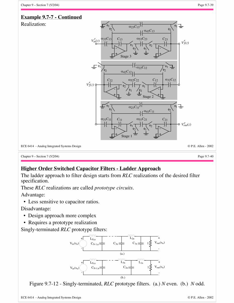
Chapter 9 – Section 7 (5/2/04) Page 9.7-39
ECE 6414 - Analog Integrated Systems Design © P.E. Allen - 2002
Example 9.7-7 - ContinuedRealization:
+-
C11
φ2α21C11
φ1
+-
C21
φ1
φ2
α51C21
φ2
φ1 Vout(z)e
α41C11
α31C11
φ1φ2
+-
C13Vin(z)e
φ2α23C13
φ1
+-
C23
φ1
φ2
α53C23
φ2
φ1V3(z)
e
α43C13
α33C13
φ1φ2
+-
C12
φ2α22C12
φ1
+-
C22
φ1
φ2
α52C22
φ2
φ1
α42C12
α32C12
φ1φ2
V2(z)e
Stage 3
Stage 2
Stage 1
Chapter 9 – Section 7 (5/2/04) Page 9.7-40
ECE 6414 - Analog Integrated Systems Design © P.E. Allen - 2002
Higher Order Switched Capacitor Filters - Ladder ApproachThe ladder approach to filter design starts from RLC realizations of the desired filterspecification.These RLC realizations are called prototype circuits.Advantage: • Less sensitive to capacitor ratios.Disadvantage: • Design approach more complex • Requires a prototype realizationSingly-terminated RLC prototype filters:
(a.)
(b.)
1
+
-
+
-
L2nLN,n
CN-1,n C3n C1nVin(sn) Vout(sn)
1
+
-
+
-
C2nCN-1,n
LN,n L3n L1n
Vin(sn) Vout(sn)
Figure 9.7-12 - Singly-terminated, RLC prototype filters. (a.) N even. (b.) N odd.
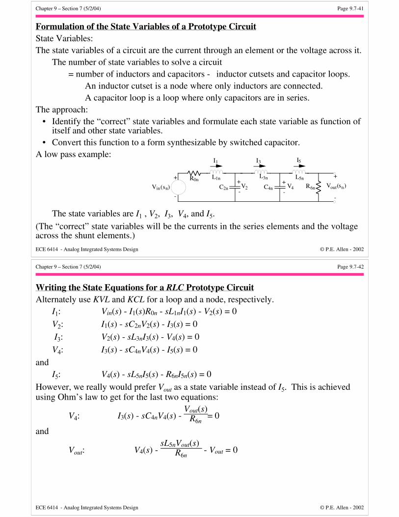
Chapter 9 – Section 7 (5/2/04) Page 9.7-41
ECE 6414 - Analog Integrated Systems Design © P.E. Allen - 2002
Formulation of the State Variables of a Prototype CircuitState Variables:The state variables of a circuit are the current through an element or the voltage across it.
The number of state variables to solve a circuit= number of inductors and capacitors - inductor cutsets and capacitor loops.
An inductor cutset is a node where only inductors are connected.A capacitor loop is a loop where only capacitors are in series.
The approach: • Identify the “correct” state variables and formulate each state variable as function of
itself and other state variables. • Convert this function to a form synthesizable by switched capacitor.
A low pass example:
The state variables are I1 , V2, I3, V4, and I5.
(The “correct” state variables will be the currents in the series elements and the voltageacross the shunt elements.)
+
-
C2n
L3nL1n
Vout(sn)+
-
Vin(sn) C4n
L5nR0n
R6n+
-
+
-
I1 I3 I5
V2 V4
Chapter 9 – Section 7 (5/2/04) Page 9.7-42
ECE 6414 - Analog Integrated Systems Design © P.E. Allen - 2002
Writing the State Equations for a RLC Prototype CircuitAlternately use KVL and KCL for a loop and a node, respectively.
I1: Vin(s) - I1(s)R0n - sL1nI1(s) - V2(s) = 0
V2: I1(s) - sC2nV2(s) - I3(s) = 0
I3: V2(s) - sL3nI3(s) - V4(s) = 0
V4: I3(s) - sC4nV4(s) - I5(s) = 0
andI5: V4(s) - sL5nI5(s) - R6nI5n(s) = 0
However, we really would prefer Vout as a state variable instead of I5. This is achievedusing Ohm’s law to get for the last two equations:
V4: I3(s) - sC4nV4(s) - Vout(s)
R6n= 0
and
Vout: V4(s) - sL5nVout(s)
R6n - Vout = 0
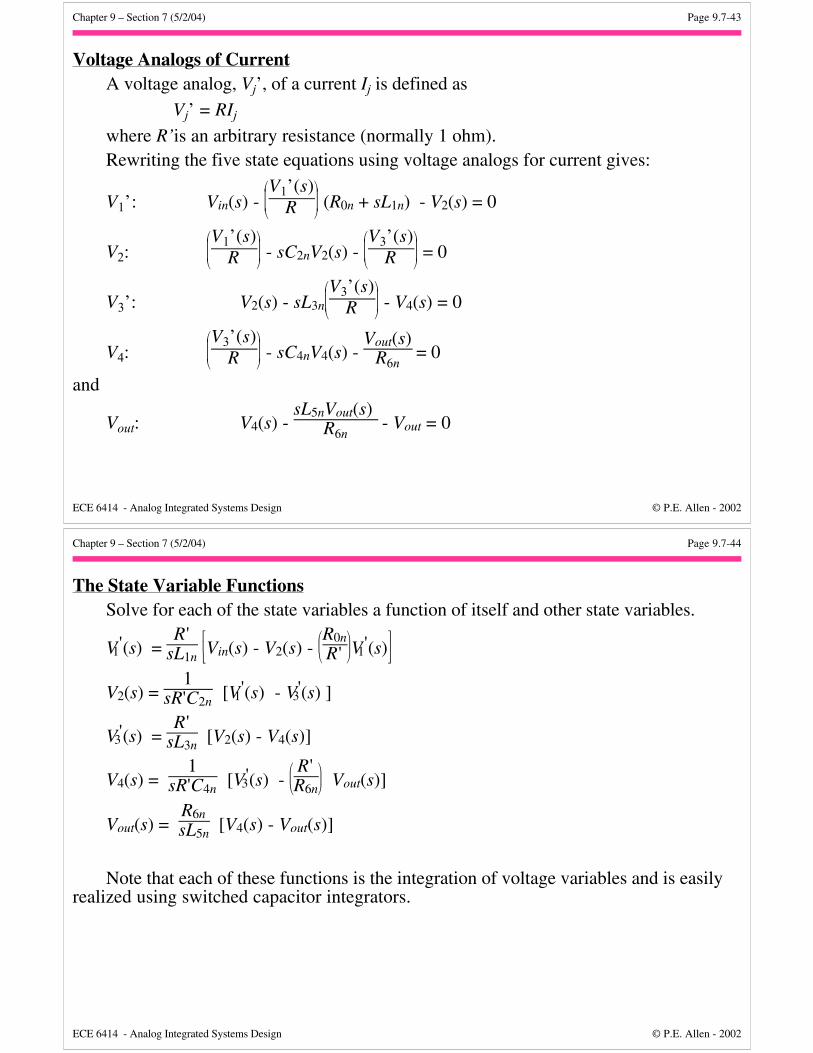
Chapter 9 – Section 7 (5/2/04) Page 9.7-43
ECE 6414 - Analog Integrated Systems Design © P.E. Allen - 2002
Voltage Analogs of CurrentA voltage analog, Vj’, of a current Ij is defined as
Vj’ = RIj
where R’is an arbitrary resistance (normally 1 ohm).Rewriting the five state equations using voltage analogs for current gives:
V1’: Vin(s) -
V1’(s)
R (R0n + sL1n) - V2(s) = 0
V2:
V1’(s)
R - sC2nV2(s) -
V3’(s)
R = 0
V3’: V2(s) - sL3n
V3’(s)
R - V4(s) = 0
V4:
V3’(s)
R - sC4nV4(s) - Vout(s)
R6n = 0
and
Vout: V4(s) - sL5nVout(s)
R6n - Vout = 0
Chapter 9 – Section 7 (5/2/04) Page 9.7-44
ECE 6414 - Analog Integrated Systems Design © P.E. Allen - 2002
The State Variable FunctionsSolve for each of the state variables a function of itself and other state variables.
V ' 1 (s) = R'
sL1n
Vin(s) - V2(s) -
R0n
R' V ' 1 (s)
V2(s) = 1
sR'C2n [V' 1 (s) - V' 3 (s) ]
V ' 3 (s) = R'
sL3n [V2(s) - V4(s)]
V4(s) = 1
sR'C4n [V' 3(s) -
R'
R6n Vout(s)]
Vout(s) = R6nsL5n
[V4(s) - Vout(s)]
Note that each of these functions is the integration of voltage variables and is easilyrealized using switched capacitor integrators.
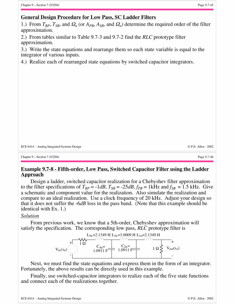
Chapter 9 – Section 7 (5/2/04) Page 9.7-45
ECE 6414 - Analog Integrated Systems Design © P.E. Allen - 2002
General Design Procedure for Low Pass, SC Ladder Filters1.) From TBP, TSB, and Ωn (or APB, ASB, and Ωn) determine the required order of the filterapproximation.2.) From tables similar to Table 9.7-3 and 9.7-2 find the RLC prototype filterapproximation.3.) Write the state equations and rearrange them so each state variable is equal to theintegrator of various inputs.4.) Realize each of rearranged state equations by switched capacitor integrators.
Chapter 9 – Section 7 (5/2/04) Page 9.7-46
ECE 6414 - Analog Integrated Systems Design © P.E. Allen - 2002
Example 9.7-8 - Fifth-order, Low Pass, Switched Capacitor Filter using the LadderApproach
Design a ladder, switched capacitor realization for a Chebyshev filter approximationto the filter specifications of TBP = -1dB, TSB = -25dB, fPB = 1kHz and fSB = 1.5 kHz. Givea schematic and component value for the realization. Also simulate the realization andcompare to an ideal realization. Use a clock frequency of 20 kHz. Adjust your design sothat it does not suffer the -6dB loss in the pass band. (Note that this example should beidentical with Ex. 1.)Solution
From previous work, we know that a 5th-order, Chebyshev approximation willsatisfy the specification. The corresponding low pass, RLC prototype filter is
1 Ω
+
-
+
-
Vin(sn) Vout(sn)1 Ω
C4n=1.0911 F
C2n=1.0911 F
L1n=2.1349 HL5n=2.1349 H L3n=3.0009 H
Next, we must find the state equations and express them in the form of an integrator.Fortunately, the above results can be directly used in this example.
Finally, use switched-capacitor integrators to realize each of the five state functionsand connect each of the realizations together.
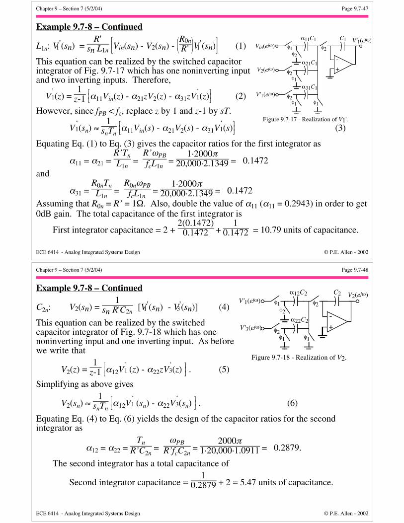
Chapter 9 – Section 7 (5/2/04) Page 9.7-47
ECE 6414 - Analog Integrated Systems Design © P.E. Allen - 2002
Example 9.7-8 – Continued
L1n: V ' 1 (sn) = R'
sn L1n
Vin(sn) - V2(sn) -
R0n
R' V ' 1 (sn) (1)
This equation can be realized by the switched capacitorintegrator of Fig. 9.7-17 which has one noninverting inputand two inverting inputs. Therefore,
V’1(z) =
1z-1
α11Vin(z) - α21zV2(z) - α31zV‘1(z) (2)
However, since fPB < fc, replace z by 1 and z-1 by sT.
V‘1(sn) ≈
1snTn
α11Vin(s) - α21V2(s) - α31V‘1(s) (3)
Equating Eq. (1) to Eq. (3) gives the capacitor ratios for the first integrator as
α11 = α21 = R’TnL1n
= R’ωPBfcL1n
= 1·2000π
20,000·2.1349 = 0.1472
and
α31 = R0nTnL1n
= R0nωPBfcL1n
= 1·2000π
20,000·2.1349 = 0.1472
Assuming that R0n = R’ = 1Ω. Also, double the value of α11 (α11 = 0.2943) in order to get0dB gain. The total capacitance of the first integrator is
First integrator capacitance = 2 + 2(0.1472)
0.1472 + 1
0.1472 = 10.79 units of capacitance.
V2(ejω)+-
V'1(ejω)
C1Vin(ejω)
φ2
φ1
φ1
φ2φ1
α21C1
α11C1
φ2
φ1
α31C1
φ2
V'1(ejω)
Figure 9.7-17 - Realization of V1'.
Chapter 9 – Section 7 (5/2/04) Page 9.7-48
ECE 6414 - Analog Integrated Systems Design © P.E. Allen - 2002
Example 9.7-8 – Continued
C2n: V2(sn) = 1
sn R'C2n [V' 1 (sn) - V' 3 (sn)] (4)
This equation can be realized by the switchedcapacitor integrator of Fig. 9.7-18 which has onenoninverting input and one inverting input. As beforewe write that
V2(z) = 1
z-1
α12V‘1 (z) - α22zV
‘3(z) . (5)
Simplifying as above gives
V2(sn) ≈ 1
snTn
α12V‘1 (sn) - α22V
‘3(sn) . (6)
Equating Eq. (4) to Eq. (6) yields the design of the capacitor ratios for the secondintegrator as
α12 = α22 = Tn
R’C2n =
ωPBR’fcC2n
= 2000π
1·20,000·1.0911 = 0.2879.
The second integrator has a total capacitance of
Second integrator capacitance = 1
0.2879 + 2 = 5.47 units of capacitance.
V'3(ejω)+-
V'1(ejω)C2
φ2
φ1 φ1
φ2φ1
α22C2
α12C2
φ2
V2(ejω)
Figure 9.7-18 - Realization of V2.
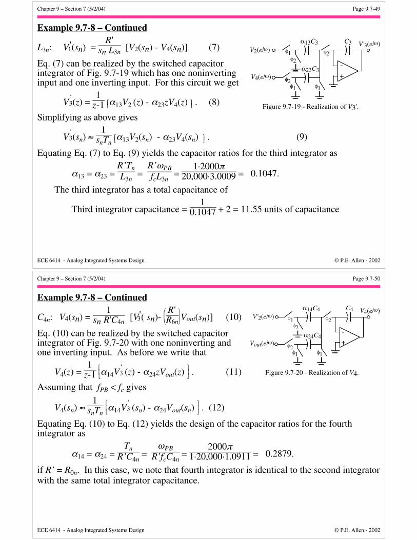
Chapter 9 – Section 7 (5/2/04) Page 9.7-49
ECE 6414 - Analog Integrated Systems Design © P.E. Allen - 2002
Example 9.7-8 – Continued
L3n: V ' 3 (sn) = R'
sn L3n [V2(sn) - V4(sn)] (7)
Eq. (7) can be realized by the switched capacitorintegrator of Fig. 9.7-19 which has one noninvertinginput and one inverting input. For this circuit we get
V‘3(z) =
1z-1 α13V2 (z) - α23zV4(z) . (8)
Simplifying as above gives
V‘3(sn) ≈
1snTn
α13V2(sn) - α23V4(sn) . (9)
Equating Eq. (7) to Eq. (9) yields the capacitor ratios for the third integrator as
α13 = α23 = R’TnL3n
= R’ωPBfcL3n
= 1·2000π
20,000·3.0009 = 0.1047.
The third integrator has a total capacitance of
Third integrator capacitance = 1
0.1047 + 2 = 11.55 units of capacitance
V4(ejω)+-
V2(ejω)C3
φ2
φ1 φ1
φ2φ1
α23C3
α13C3
φ2
V'3(ejω)
Figure 9.7-19 - Realization of V3'.
Chapter 9 – Section 7 (5/2/04) Page 9.7-50
ECE 6414 - Analog Integrated Systems Design © P.E. Allen - 2002
Example 9.7-8 – Continued
C4n: V4(sn) = 1
sn R'C4n [V' 3( sn)-
R'
R6nVout(sn)] (10)
Eq. (10) can be realized by the switched capacitorintegrator of Fig. 9.7-20 with one noninverting andone inverting input. As before we write that
V4(z) = 1
z-1
α14V‘3 (z) - α24zVout(z) . (11)
Assuming that fPB < fc gives
V4(sn) ≈ 1
snTn
α14V‘3 (sn) - α24Vout(sn) . (12)
Equating Eq. (10) to Eq. (12) yields the design of the capacitor ratios for the fourthintegrator as
α14 = α24 = Tn
R’C4n =
ωPBR’fcC4n
= 2000π
1·20,000·1.0911 = 0.2879.
if R’ = R0n. In this case, we note that fourth integrator is identical to the second integratorwith the same total integrator capacitance.
Vout(ejω)+-
V'2(ejω)C4
φ2
φ1 φ1
φ2φ1
α24C4
α14C4
φ2
V4(ejω)
Figure 9.7-20 - Realization of V4.
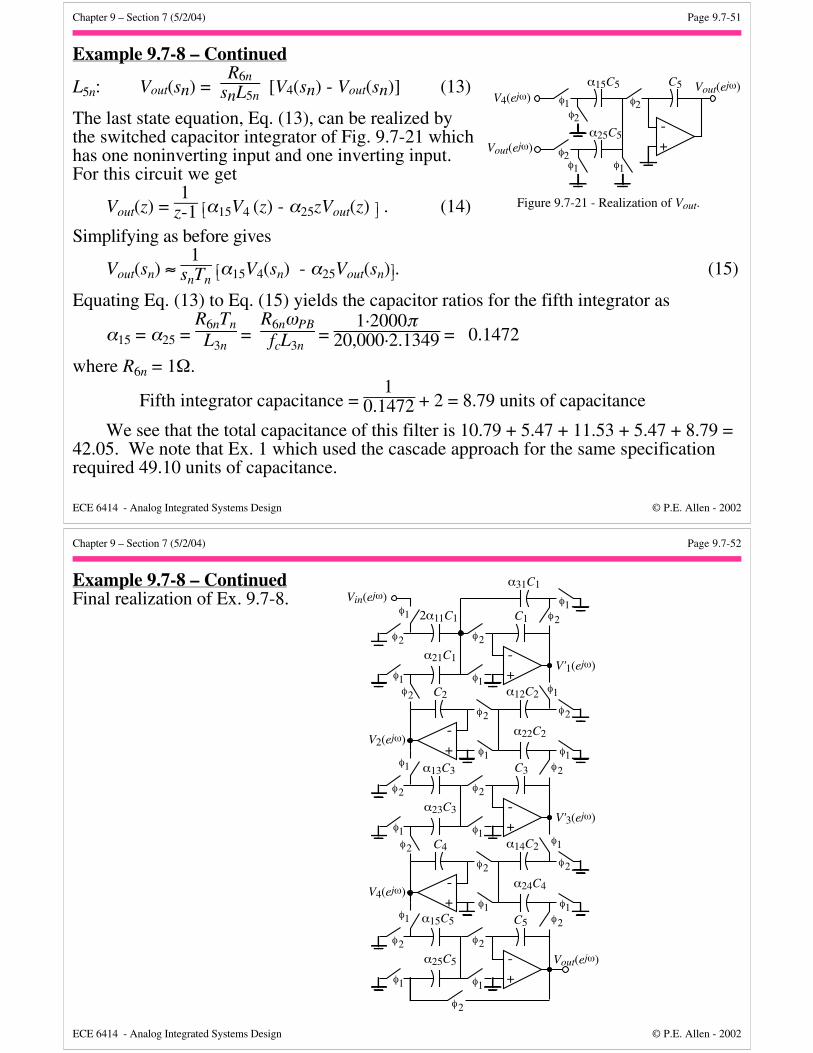
Chapter 9 – Section 7 (5/2/04) Page 9.7-51
ECE 6414 - Analog Integrated Systems Design © P.E. Allen - 2002
Example 9.7-8 – Continued
L5n: Vout(sn) = R6n
snL5n [V4(sn) - Vout(sn)] (13)
The last state equation, Eq. (13), can be realized bythe switched capacitor integrator of Fig. 9.7-21 whichhas one noninverting input and one inverting input.For this circuit we get
Vout(z) = 1
z-1 α15V4 (z) - α25zVout(z) . (14)
Simplifying as before gives
Vout(sn) ≈ 1
snTn α15V4(sn) - α25Vout(sn) . (15)
Equating Eq. (13) to Eq. (15) yields the capacitor ratios for the fifth integrator as
α15 = α25 = R6nTnL3n
= R6nωPBfcL3n
= 1·2000π
20,000·2.1349 = 0.1472
where R6n = 1Ω.
Fifth integrator capacitance = 1
0.1472 + 2 = 8.79 units of capacitance
We see that the total capacitance of this filter is 10.79 + 5.47 + 11.53 + 5.47 + 8.79 =42.05. We note that Ex. 1 which used the cascade approach for the same specificationrequired 49.10 units of capacitance.
Vout(ejω)+-
V4(ejω)C5
φ2
φ1 φ1
φ2φ1
α25C5
α15C5
φ2
Vout(ejω)
Figure 9.7-21 - Realization of Vout.
Chapter 9 – Section 7 (5/2/04) Page 9.7-52
ECE 6414 - Analog Integrated Systems Design © P.E. Allen - 2002
Example 9.7-8 – ContinuedFinal realization of Ex. 9.7-8.
V2(ejω)
C1
Vin(ejω)
φ2
φ1
α21C1
2α11C1
α31C1
V'1(ejω)
C2
α22C2
α12C2
+-
+-
φ1
φ2
φ2
φ2
φ1
φ1
φ1
φ1
φ1
φ1
φ2 φ2
φ2C3
φ2
φ1
α23C3
α13C3
V'3(ejω)+-
φ1
φ2
φ1
V4(ejω)
C4
α24C4
α14C2
+-
φ1 φ1
φ2 φ2
φ2φ1
φ2
φ2
α25C5 Vout(ejω)+-
φ1
φ2
φ1
φ2
C5α15C5
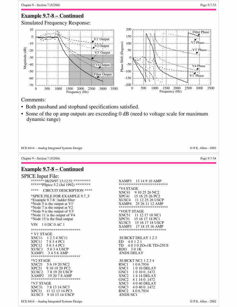
Chapter 9 – Section 7 (5/2/04) Page 9.7-53
ECE 6414 - Analog Integrated Systems Design © P.E. Allen - 2002
Example 9.7-8 – ContinuedSimulated Frequency Response:
Frequency (Hz)
-70
-60
-50
-40
-30
-20
-10
0
10
0 500 1000 1500 2000 2500 3000 3500
Mag
nitu
de (d
B)
V1' Output
V2 Output
V3' Output
V4 Output
Filter Output
-200
-150
-100
-50
0
50
100
150
200
0 500 1000 1500 2000 2500 3000 3500
Phas
e Sh
ift (
Deg
rees
)
Frequency (Hz)
V1' Phase
V2 Phase
V3' Phase
V4 Phase
Filter Phase
Comments:• Both passband and stopband specifications satisfied.• Some of the op amp outputs are exceeding 0 dB (need to voltage scale for maximum dynamic range)
Chapter 9 – Section 7 (5/2/04) Page 9.7-54
ECE 6414 - Analog Integrated Systems Design © P.E. Allen - 2002
Example 9.7-8 – ContinuedSPICE Input File:
******* 08/29/97 13:12:51 ***************PSpice 5.2 (Jul 1992) ********
**** CIRCUIT DESCRIPTION ****
*SPICE FILE FOR EXAMPLE 9.7_5*Example 9.7-8 : ladder filter*Node 5 is the output at V1'*Node 7 is the output at V2*Node 9 is the output of V3'*Node 11 is the output of V4*Node 15 is the final output
VIN 1 0 DC 0 AC 1
*************************** V1' STAGEXNC11 1 2 3 4 NC11XPC11 7 8 3 4 PC1XPC12 5 6 3 4 PC1XUSC1 5 6 3 4 USCPXAMP1 3 4 5 6 AMP***************************V2 STAGEXNC21 5 6 19 20 NC2XPC21 9 10 19 20 PC2XUSC2 7 8 19 20 USCPXAMP2 19 20 7 8 AMP***************************V3' STAGEXNC31 7 8 13 14 NC3XPC31 11 12 13 14 PC3XUSC3 9 10 13 14 USCP
XAMP3 13 14 9 10 AMP***************************V4 STAGEXNC41 9 10 25 26 NC2XPC41 15 16 25 26 PC2XUSC4 11 12 25 26 USCPXAMP4 25 26 11 12 AMP***************************VOUT STAGEXNC51 11 12 17 18 NC1XPC51 15 16 17 18 PC1XUSC5 15 16 17 18 USCPXAMP5 17 18 15 16 AMP*************************
.SUBCKT DELAY 1 2 3ED 4 0 1 2 1TD 4 0 3 0 ZO=1K TD=25USRDO 3 0 1K.ENDS DELAY
.SUBCKT NC1 1 2 3 4RNC1 1 0 6.7934XNC1 1 0 10 DELAYGNC1 1 0 10 0 .1472XNC2 1 4 14 DELAYGNC2 4 1 14 0 .1472XNC3 4 0 40 DELAYGNC3 4 0 40 0 .1472RNC2 4 0 6.7934.ENDS NC1
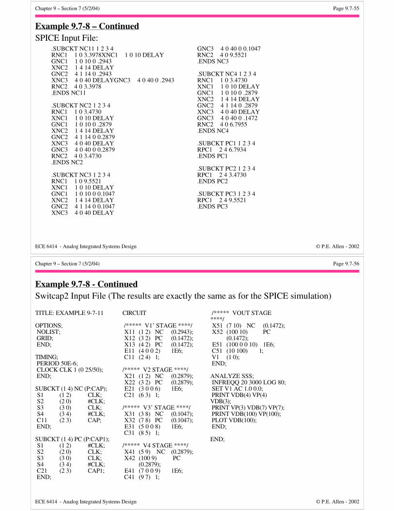
Chapter 9 – Section 7 (5/2/04) Page 9.7-55
ECE 6414 - Analog Integrated Systems Design © P.E. Allen - 2002
Example 9.7-8 – ContinuedSPICE Input File:
.SUBCKT NC11 1 2 3 4RNC1 1 0 3.3978XNC1 1 0 10 DELAYGNC1 1 0 10 0 .2943XNC2 1 4 14 DELAYGNC2 4 1 14 0 .2943XNC3 4 0 40 DELAYGNC3 4 0 40 0 .2943RNC2 4 0 3.3978.ENDS NC11
.SUBCKT NC2 1 2 3 4RNC1 1 0 3.4730XNC1 1 0 10 DELAYGNC1 1 0 10 0 .2879XNC2 1 4 14 DELAYGNC2 4 1 14 0 0.2879XNC3 4 0 40 DELAYGNC3 4 0 40 0 0.2879RNC2 4 0 3.4730.ENDS NC2
.SUBCKT NC3 1 2 3 4RNC1 1 0 9.5521XNC1 1 0 10 DELAYGNC1 1 0 10 0 0.1047XNC2 1 4 14 DELAYGNC2 4 1 14 0 0.1047XNC3 4 0 40 DELAY
GNC3 4 0 40 0 0.1047RNC2 4 0 9.5521.ENDS NC3
.SUBCKT NC4 1 2 3 4RNC1 1 0 3.4730XNC1 1 0 10 DELAYGNC1 1 0 10 0 .2879XNC2 1 4 14 DELAYGNC2 4 1 14 0 .2879XNC3 4 0 40 DELAYGNC3 4 0 40 0 .1472RNC2 4 0 6.7955.ENDS NC4
.SUBCKT PC1 1 2 3 4RPC1 2 4 6.7934.ENDS PC1
.SUBCKT PC2 1 2 3 4RPC1 2 4 3.4730.ENDS PC2
.SUBCKT PC3 1 2 3 4RPC1 2 4 9.5521.ENDS PC3
Chapter 9 – Section 7 (5/2/04) Page 9.7-56
ECE 6414 - Analog Integrated Systems Design © P.E. Allen - 2002
Example 9.7-8 - ContinuedSwitcap2 Input File (The results are exactly the same as for the SPICE simulation)
TITLE: EXAMPLE 9-7-11
OPTIONS; NOLIST; GRID; END;
TIMING; PERIOD 50E-6; CLOCK CLK 1 (0 25/50); END;
SUBCKT (1 4) NC (P:CAP); S1 (1 2) CLK; S2 (2 0) #CLK; S3 (3 0) CLK; S4 (3 4) #CLK; C11 (2 3) CAP; END;
SUBCKT (1 4) PC (P:CAP1); S1 (1 2) #CLK; S2 (2 0) CLK; S3 (3 0) CLK; S4 (3 4) #CLK; C21 (2 3) CAP1; END;
CIRCUIT
/***** V1’ STAGE ****/ X11 (1 2) NC (0.2943); X12 (3 2) PC (0.1472); X13 (4 2) PC (0.1472); E11 (4 0 0 2) 1E6; C11 (2 4) 1;
/***** V2 STAGE ****/ X21 (1 2) NC (0.2879); X22 (3 2) PC (0.2879); E21 (3 0 0 6) 1E6; C21 (6 3) 1;
/***** V3’ STAGE ****/ X31 (3 8) NC (0.1047); X32 (7 8) PC (0.1047); E31 (5 0 0 8) 1E6; C31 (8 5) 1;
/***** V4 STAGE ****/ X41 (5 9) NC (0.2879); X42 (100 9) PC
(0.2879); E41 (7 0 0 9) 1E6; C41 (9 7) 1;
/***** VOUT STAGE****/ X51 (7 10) NC (0.1472); X52 (100 10) PC
(0.1472); E51 (100 0 0 10) 1E6; C51 (10 100) 1; V1 (1 0); END;
ANALYZE SSS; INFREQQ 20 3000 LOG 80; SET V1 AC 1.0 0.0; PRINT VDB(4) VP(4)VDB(3); PRINT VP(3) VDB(7) VP(7); PRINT VDB(100) VP(100); PLOT VDB(100); END;
END;
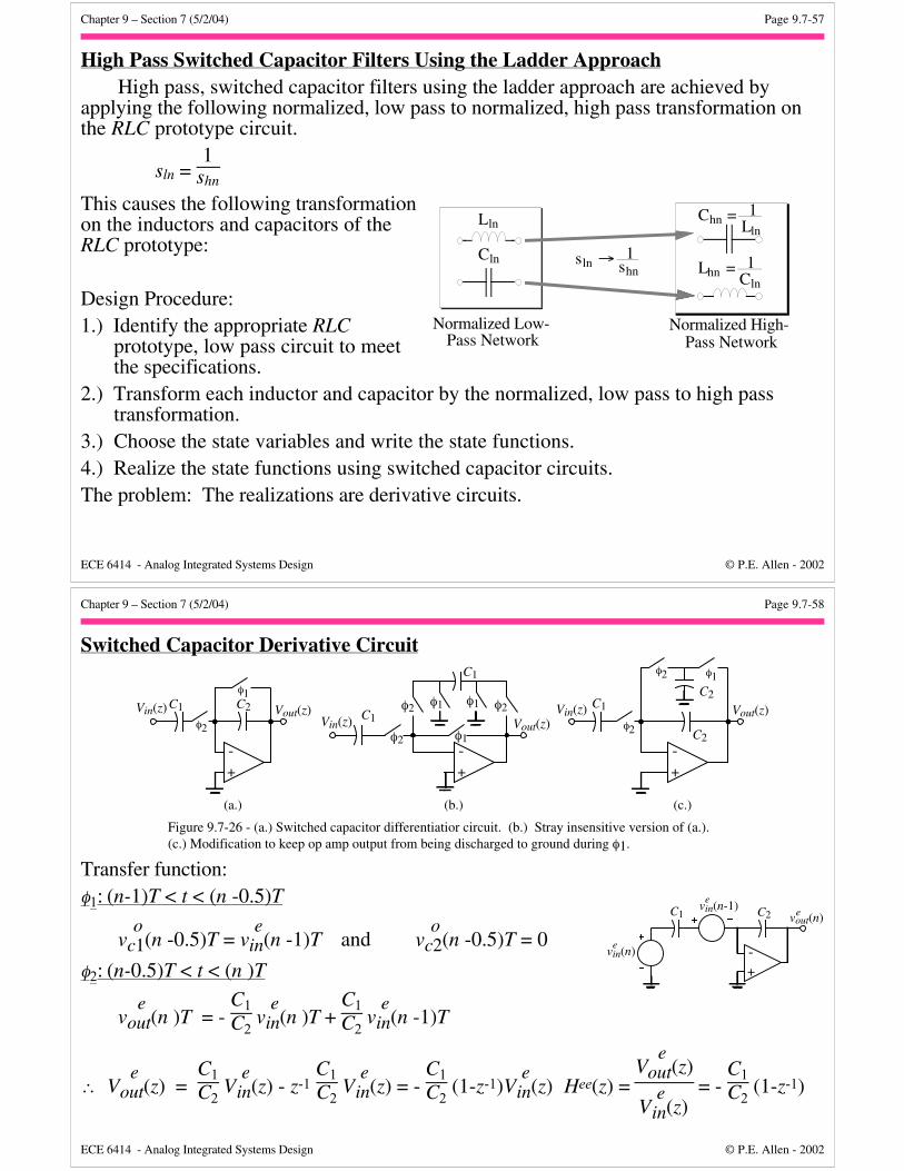
Chapter 9 – Section 7 (5/2/04) Page 9.7-57
ECE 6414 - Analog Integrated Systems Design © P.E. Allen - 2002
High Pass Switched Capacitor Filters Using the Ladder ApproachHigh pass, switched capacitor filters using the ladder approach are achieved by
applying the following normalized, low pass to normalized, high pass transformation onthe RLC prototype circuit.
sln = 1
shn
This causes the following transformationon the inductors and capacitors of theRLC prototype:
Design Procedure:1.) Identify the appropriate RLC
prototype, low pass circuit to meetthe specifications.
2.) Transform each inductor and capacitor by the normalized, low pass to high passtransformation.
3.) Choose the state variables and write the state functions.4.) Realize the state functions using switched capacitor circuits.The problem: The realizations are derivative circuits.
sln → 1shn
Normalized Low-Pass Network
Normalized High-Pass Network
Lln
ClnLhn = 1
Cln
Chn = 1Lln
Chapter 9 – Section 7 (5/2/04) Page 9.7-58
ECE 6414 - Analog Integrated Systems Design © P.E. Allen - 2002
Switched Capacitor Derivative Circuit
+-
Vin(z) C2
φ2
φ1C1 Vout(z)
Figure 9.7-26 - (a.) Switched capacitor differentiatior circuit. (b.) Stray insensitive version of (a.). (c.) Modification to keep op amp output from being discharged to ground during φ1.
+-
Vin(z)
C2φ2
φ1
C1 Vout(z)
φ2
C2
(a.) (b.)
+-
C1
C1
φ1 φ1
φ1
φ2φ2
φ2Vout(z)Vin(z)
(c.)
Transfer function:φ1: (n-1)T < t < (n -0.5)T
v oc1(n -0.5)T = v
ein(n -1)T and v
oc2(n -0.5)T = 0
φ2: (n-0.5)T < t < (n )T
v e
out(n )T = - C1C2
v ein(n )T +
C1C2
v ein(n -1)T
∴ V e
out(z) = C1C2
V ein(z) - z-1
C1C2
V ein(z) = -
C1C2
(1-z-1)V ein(z) Hee(z) =
V e
out(z)
V ein(z)
= - C1C2
(1-z-1)
+-vin(n)
C1 C2
e
vin(n-1)e
vout(n)e
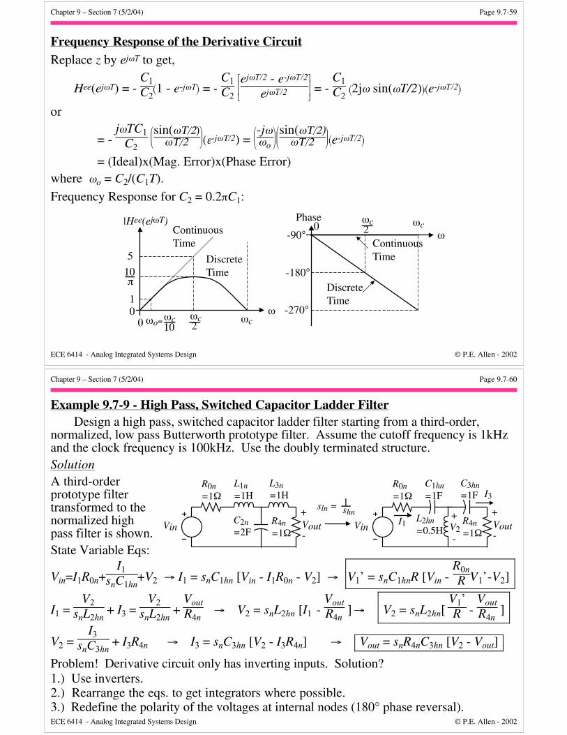
Chapter 9 – Section 7 (5/2/04) Page 9.7-59
ECE 6414 - Analog Integrated Systems Design © P.E. Allen - 2002
Frequency Response of the Derivative CircuitReplace z by ejωT to get,
Hee(ejωT) = - C1C2
1 - e-jωT = - C1C2
ejωT/2 - e-jωT/2
ejωT/2 = - C1C2
2jω sin(ωT/2) e-jωT/2
or
= - jωTC1
C2
sin(ωΤ/2)
ωΤ/2 (ε-jωΤ/2) =
-jω
ωo
sin(ωΤ/2)
ωΤ/2 e-jωT/2
= (Ideal)x(Mag. Error)x(Phase Error)where ωo = C2/(C1T).
Frequency Response for C2 = 0.2πC1:
|Hee(ejωT)
5
10
10
0 ωo= ωc2
ωc10
ωc
ContinuousTime
DiscreteTime
π
ω
Phase
-90°
-180°
-270°
0ωc2
ωcω
ContinuousTime
DiscreteTime
Chapter 9 – Section 7 (5/2/04) Page 9.7-60
ECE 6414 - Analog Integrated Systems Design © P.E. Allen - 2002
Example 9.7-9 - High Pass, Switched Capacitor Ladder FilterDesign a high pass, switched capacitor ladder filter starting from a third-order,
normalized, low pass Butterworth prototype filter. Assume the cutoff frequency is 1kHzand the clock frequency is 100kHz. Use the doubly terminated structure.SolutionA third-orderprototype filtertransformed to thenormalized highpass filter is shown.State Variable Eqs:
Vin=I1R0n+I1
snC1hn+V2 → I1 = snC1hn [Vin - I1R0n - V2] → V1’ = snC1hnR [Vin -
R0nR V1’-V2]
I1 = V2
snL2hn + I3 =
V2snL2hn
+ VoutR4n
→ V2 = snL2hn [I1 - VoutR4n
]→ V2 = snL2hn[ V1’R -
VoutR4n
]
V2 = I3
snC3hn + I3R4n → I3 = snC3hn [V2 - I3R4n] → Vout = snR4nC3hn [V2 - Vout]
Problem! Derivative circuit only has inverting inputs. Solution?1.) Use inverters.2.) Rearrange the eqs. to get integrators where possible.3.) Redefine the polarity of the voltages at internal nodes (180° phase reversal).
Vin
R0n=1Ω
L1n=1H
L3n=1H
C2n=2F
R4n=1Ω
+
-Vout
sln = shn1
Vin
R0n=1Ω
C1hn=1F
C3hn=1F
L2hn=0.5H
R4n=1Ω
+
-VoutI1
I3
+
-V2
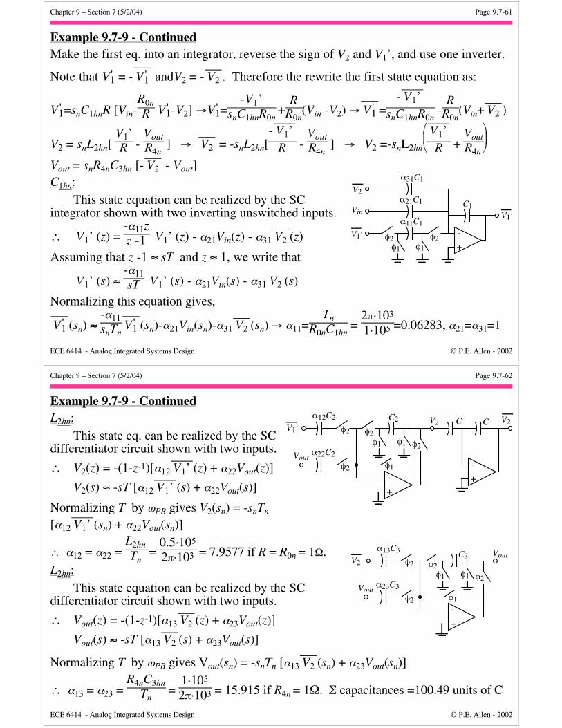
Chapter 9 – Section 7 (5/2/04) Page 9.7-61
ECE 6414 - Analog Integrated Systems Design © P.E. Allen - 2002
Example 9.7-9 - ContinuedMake the first eq. into an integrator, reverse the sign of V2 and V1’, and use one inverter.
Note that V '1 = - V '1 andV2 = - V2 . Therefore the rewrite the first state equation as:
V '1=snC1hnR [Vin-R0nR V '1-V2] →V '1=
-V1’snC1hnR0n
+R
R0n(Vin -V2) → V '1 =
- V1’snC1hnR0n
-R
R0n(Vin+ V2 )
V2 = snL2hn[ V1’R -
VoutR4n
] → V2 = -snL2hn[- V1’
R - VoutR4n
] → V2 =-snL2hn
V1’
R + VoutR4n
Vout = snR4nC3hn [- V2 - Vout]C1hn:
This state equation can be realized by the SCintegrator shown with two inverting unswitched inputs.
∴ V1’ (z) = -α11zz -1 V1’ (z) - α21Vin(z) - α31 V2 (z)
Assuming that z -1 ≈ sT and z ≈ 1, we write that
V1’ (s) ≈ -α11sT V1’ (s) - α21Vin(s) - α31 V2 (s)
Normalizing this equation gives,
V '1 (sn) ≈ -α11snTn
V '1 (sn)-α21Vin(sn)-α31 V2 (sn) → α11=Tn
R0nC1hn =
2π·103
1·105 =0.06283, α21=α31=1
+-
α11C1
φ1 φ1
α21C1
α31C1
C1
V1'
V2
Vin V1'
φ2 φ2
Chapter 9 – Section 7 (5/2/04) Page 9.7-62
ECE 6414 - Analog Integrated Systems Design © P.E. Allen - 2002
Example 9.7-9 - ContinuedL2hn:
This state eq. can be realized by the SCdifferentiator circuit shown with two inputs.
∴ V2(z) = -(1-z-1)[α12 V1’ (z) + α22Vout(z)]
V2(s) ≈ -sT [α12 V1’ (s) + α22Vout(s)]
Normalizing T by ωPB gives V2(sn) = -snTn
[α12 V1’ (sn) + α22Vout(sn)]
∴ α12 = α22 = L2hnTn
= 0.5·105
2π·103 = 7.9577 if R = R0n = 1Ω.
L2hn:
This state equation can be realized by the SCdifferentiator circuit shown with two inputs.
∴ Vout(z) = -(1-z-1)[α13 V2 (z) + α23Vout(z)]
Vout(s) ≈ -sT [α13 V2 (s) + α23Vout(s)]
Normalizing T by ωPB gives Vout(sn) = -snTn [α13 V2 (sn) + α23Vout(sn)]
∴ α13 = α23 = R4nC3hn
Tn =
1·105
2π·103 = 15.915 if R4n = 1Ω. Σ capacitances =100.49 units of C
+-
C2
φ1 φ1
φ1
φ2
φ2
φ2
V2
Voutα22C2
φ2
α12C2
V1'
+-
C C V2
+-
C3
φ1 φ1
φ1
φ2
φ2
φ2
Vout
Voutα23C3
φ2
α13C3
V2
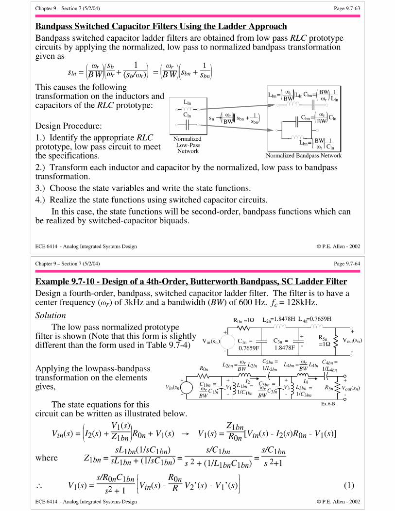
Chapter 9 – Section 7 (5/2/04) Page 9.7-63
ECE 6414 - Analog Integrated Systems Design © P.E. Allen - 2002
Bandpass Switched Capacitor Filters Using the Ladder ApproachBandpass switched capacitor ladder filters are obtained from low pass RLC prototypecircuits by applying the normalized, low pass to normalized bandpass transformationgiven as
sln =
ωr
BW
sb
ωr + 1
(sb/ωr) =
ωr
BW
sbn + 1
sbn
This causes the followingtransformation on the inductors andcapacitors of the RLC prototype:
Design Procedure:1.) Identify the appropriate RLCprototype, low pass circuit to meetthe specifications.2.) Transform each inductor and capacitor by the normalized, low pass to bandpasstransformation.3.) Choose the state variables and write the state functions.4.) Realize the state functions using switched capacitor circuits.
In this case, the state functions will be second-order, bandpass functions which canbe realized by switched-capacitor biquads.
NormalizedLow-PassNetwork
Lln
Cln sn → ωrBW
sbn + 1sbn
Normalized Bandpass Network
Lbn= ωrBW
Lln Cbn= BWωr
1Lln
Lbn= BWωr
1Cln
Cbn = ωrBW
Cln
Chapter 9 – Section 7 (5/2/04) Page 9.7-64
ECE 6414 - Analog Integrated Systems Design © P.E. Allen - 2002
Example 9.7-10 - Design of a 4th-Order, Butterworth Bandpass, SC Ladder FilterDesign a fourth-order, bandpass, switched capacitor ladder filter. The filter is to have acenter frequency (ωr) of 3kHz and a bandwidth (BW) of 600 Hz. fc = 128kHz.
SolutionThe low pass normalized prototype
filter is shown (Note that this form is slightlydifferent than the form used in Table 9.7-4)
Applying the lowpass-bandpasstransformation on the elementsgives,
The state equations for thiscircuit can be written as illustrated below.
Vin(s) =
I2(s) + V1(s)Z1bn R0n + V1(s) → V1(s) =
Z1bnR0n [Vin(s) - I2(s)R0n - V1(s)]
where Z1bn = sL1bn(1/sC1bn)
sL1bn + (1/sC1bn) = s/C1bn
s 2 + (1/L1bnC1bn) =
s/C1bn
s 2+1
∴ V1(s) = s/R0nC1bn
s2 + 1
Vin(s) - R0nR V2’(s) - V1’(s) (1)
+
-
C1n
L2n
Vout(sn)+
-
Vin(sn)
R0n
R5n+
-
=1Ω
0.7659F=
=1.8478H
C3n1.8478F
=
L =0.7659H4n
=1Ω
C1bn = C1lnωr
BW
L1bn =1/C1bn
+
-V1
R0n
Vin(sn)
L2bn = L2lnωr
BWC2bn =1/L2bn
I2 C3bn = C3lnBW
L3bn =1/C3bn
+
-V3
L4bn = L4lnωr
BWC4bn =1/L4bn
I4ωr
+
-Vout(sn)R5n
Ex.6-B
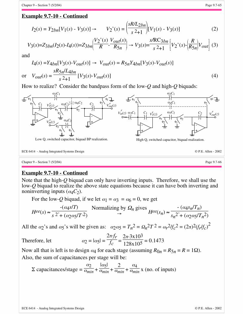
Chapter 9 – Section 7 (5/2/04) Page 9.7-65
ECE 6414 - Analog Integrated Systems Design © P.E. Allen - 2002
Example 9.7-10 - Continued
I2(s) = Y2bn[V1(s) - V3(s)]→ V2’(s) =
sR/L2bn
s 2+1[V1(s) - V3(s)] (2)
V3(s)=Z3bn(I2(s)-I4(s))=Z3bn
V2’(s)
R -Vout(s)
R5n → V3(s)=s/RC3bn
s 2+1
V2’(s)-
R
R5n Vout (3)
andI4(s) =Y4bn[V3(s)-Vout(s)] → Vout(s) = R5nY4bn[V3(s)-Vout(s)]
or Vout(s) = sR5n/L4bn
s 2+1 [V3(s)-Vout(s)] (4)
How to realize? Consider the bandpass form of the low-Q and high-Q biquads:
+-
V1(z)C1
Low Q, switched capacitor, biquad BP realization.
Vin(z)e
φ1 φ1φ2
φ2
α2C1
α4C2
φ2
+-
C2
φ2
α6C2
φ2
α5C2
φ1
Vout(z)ee
φ1φ1+-
V1(z)C1Vin(z)e
φ1φ2
α2C1
+-
C2
φ1
φ2
α5C2
φ2
φ1
Vout(z)e
α4C1
eα3C1
High Q, switched capacitor, biquad realization.
φ1φ2
Chapter 9 – Section 7 (5/2/04) Page 9.7-66
ECE 6414 - Analog Integrated Systems Design © P.E. Allen - 2002
Example 9.7-10 - ContinuedNote that the high-Q biquad can only have inverting inputs. Therefore, we shall use thelow-Q biquad to realize the above state equations because it can have both inverting andnoninverting inputs (α4C2).
For the low-Q biquad, if we let α1 = α3 = α6 = 0, we get
Hee(s) ≈ -(α4s/T)
s 2˚+ (α2α5/T˚2)Normalizing by Ωn gives
→ Hee(sn) ≈ - (α4sn/Tn)
sn2˚+ (α2α5/Tn2)
All the α2’s and α5’s will be given as: α2α5 = Tn2 = Ωn2T 2 = ωr2/fc2 = (2π)2(fr/fc)2
Therefore, let α2 = |α5| = 2π·fr
fc = 2π·3x103
128x105 = 0.1473
Now all that is left is to design α4 for each stage (assuming R0n = R5n = R = 1Ω).Also, the sum of capacitances per stage will be:
Σ capacitances/stage = α2αmin +
|α5|αmin +
2αmin +
α4αmin x (no. of inputs)
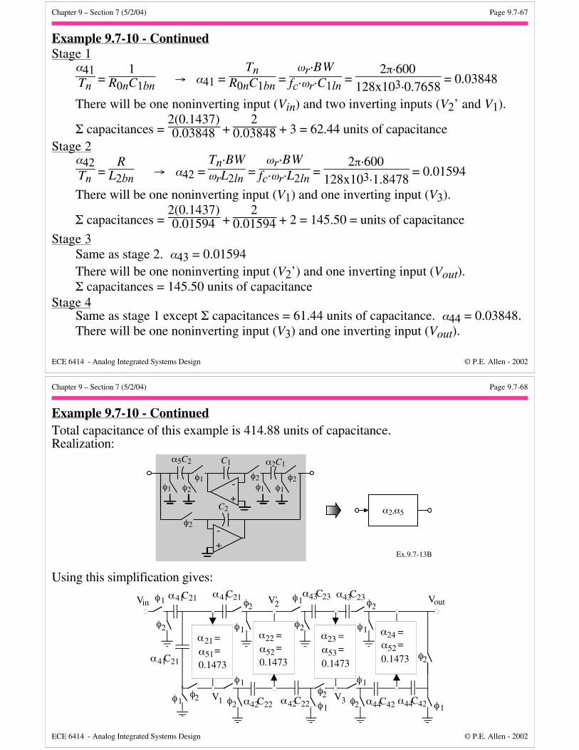
Chapter 9 – Section 7 (5/2/04) Page 9.7-67
ECE 6414 - Analog Integrated Systems Design © P.E. Allen - 2002
Example 9.7-10 - ContinuedStage 1
α41Tn =
1R0nC1bn → α41 =
TnR0nC1bn =
ωr·BWfc·ωr·C1ln =
2π·600128x103·0.7658
= 0.03848
There will be one noninverting input (Vin) and two inverting inputs (V2’ and V1).
Σ capacitances = 2(0.1437)0.03848 +
20.03848 + 3 = 62.44 units of capacitance
Stage 2α42Tn =
RL2bn → α42 =
Tn·BWωrL2ln =
ωr·BWfc·ωr·L2ln =
2π·600128x103·1.8478
= 0.01594
There will be one noninverting input (V1) and one inverting input (V3).
Σ capacitances = 2(0.1437)0.01594 +
20.01594 + 2 = 145.50 = units of capacitance
Stage 3Same as stage 2. α43 = 0.01594There will be one noninverting input (V2’) and one inverting input (Vout).Σ capacitances = 145.50 units of capacitance
Stage 4Same as stage 1 except Σ capacitances = 61.44 units of capacitance. α44 = 0.03848.There will be one noninverting input (V3) and one inverting input (Vout).
Chapter 9 – Section 7 (5/2/04) Page 9.7-68
ECE 6414 - Analog Integrated Systems Design © P.E. Allen - 2002
Example 9.7-10 - ContinuedTotal capacitance of this example is 414.88 units of capacitance.Realization:
Using this simplification gives:
φ2
φ1 α C41 21
φ1φ2
α C41 21
α 21 =α 51=
0.1473
φ2
α C41 21
φ1
φ1
φ2 α C42 22
α 22 =α 52 =
0.1473
V1
V'2
φ2
φ1α C43 23
α 23 =α 53 =
0.1473
φ2α C42 22 φ1
φ1
φ2 α C44 42V3
φ2
α C43 23
φ1
α C44 42 φ1
φ2
α 24 =α 52 =
0.1473
VoutVin
+-
+-
α2C1C1
C2
φ1φ1
φ2φ2
α5C2
φ2φ1
φ1
φ2
α2,α5
Ex.9.7-13B
Chapter 9 – Section 7 (5/2/04) Page 9.7-69
ECE 6414 - Analog Integrated Systems Design © P.E. Allen - 2002
General Approach to Designing Switched Capacitor Ladder Filters
ChooseState
Variables
WriteState
Equations
Use SC Integrators toDesign Each
State Equation
Low PassSwitchedCapacitor
Filter
Use SC BP Ckts. to
Design EachState Equation
BandpassSwitchedCapacitor
Filter
Normalized LPto Normalized
BandpassTransformation
Use SC Differentiatorsto Design EachState Equation
High PassSwitchedCapacitor
Filter
Normalized LPto Normalized
BandpassTransformation
Use SC BS Ckts. toDesign Each
State Equation
BandstopSwitchedCapacitor
Filter
EliminateL-cutsets
and C-loops
Low passPrototypeRLC Ckt.
ChooseState
Variables
WriteState
Equations
Normalized LPto Normalized
High passTransformation
ChooseState
Variables
WriteState
Equations
Normalized LPto Normalized
High passTransformation
ChooseState
Variables
WriteState
Equations
Chapter 9 – Section 7 (5/2/04) Page 9.7-70
ECE 6414 - Analog Integrated Systems Design © P.E. Allen - 2002
ANTI-ALIASING IN SWITCHED CAPACITOR FILTERSA characteristic of circuits that sample the signal (switched capacitor circuits) is that
the signal passbands occur at each harmonic of the clock frequency including thefundamental.
T(jω)
T(j0)T(jωPB)
ωPB
00
ω
Figure 9.7-28 - Spectrum of a discrete-time filter and a continuous-time anti-aliasing filter.
-ωPB ωc 2ωc
ωc+ωPBωc-ωPB 2ωc-ωPB 2ωc+ωPB
Anti-Aliasing Filter
Baseband
The primary problem of aliasing is that there are undesired passbands that contributeto the noise in the desired baseband.
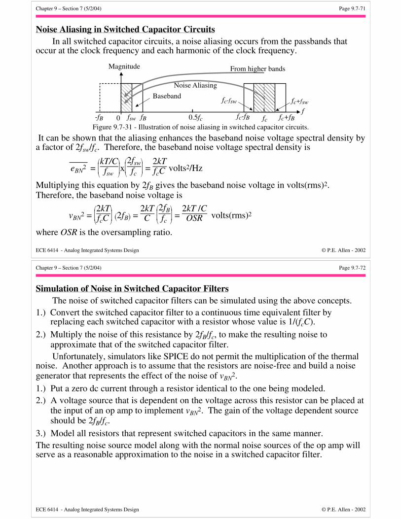
Chapter 9 – Section 7 (5/2/04) Page 9.7-71
ECE 6414 - Analog Integrated Systems Design © P.E. Allen - 2002
Noise Aliasing in Switched Capacitor CircuitsIn all switched capacitor circuits, a noise aliasing occurs from the passbands that
occur at the clock frequency and each harmonic of the clock frequency.
f0.5fc fcfBfsw-fB
fc-fsw
fc+fBfc-fB
fc+fsw
Magnitude
0
Noise Aliasing
From higher bands
Baseband
Figure 9.7-31 - Illustration of noise aliasing in switched capacitor circuits.
It can be shown that the aliasing enhances the baseband noise voltage spectral density bya factor of 2fsw/fc. Therefore, the baseband noise voltage spectral density is
eBN2 =
kT/C
fsw x
2fsw
fc =
2kTfcC volts2/Hz
Multiplying this equation by 2fB gives the baseband noise voltage in volts(rms)2.Therefore, the baseband noise voltage is
vBN2 =
2kT
fcC 2fB = 2kTC
2fB
fc =
2kT /COSR volts(rms)2
where OSR is the oversampling ratio.
Chapter 9 – Section 7 (5/2/04) Page 9.7-72
ECE 6414 - Analog Integrated Systems Design © P.E. Allen - 2002
Simulation of Noise in Switched Capacitor FiltersThe noise of switched capacitor filters can be simulated using the above concepts.
1.) Convert the switched capacitor filter to a continuous time equivalent filter byreplacing each switched capacitor with a resistor whose value is 1/(fcC).
2.) Multiply the noise of this resistance by 2fB/fc, to make the resulting noise toapproximate that of the switched capacitor filter.Unfortunately, simulators like SPICE do not permit the multiplication of the thermal
noise. Another approach is to assume that the resistors are noise-free and build a noisegenerator that represents the effect of the noise of vBN
2.
1.) Put a zero dc current through a resistor identical to the one being modeled.2.) A voltage source that is dependent on the voltage across this resistor can be placed at
the input of an op amp to implement vBN2. The gain of the voltage dependent source
should be 2fB/fc.
3.) Model all resistors that represent switched capacitors in the same manner.The resulting noise source model along with the normal noise sources of the op amp willserve as a reasonable approximation to the noise in a switched capacitor filter.
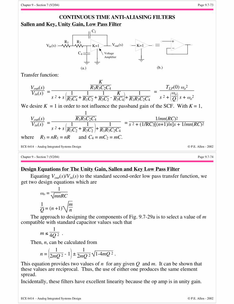
Chapter 9 – Section 7 (5/2/04) Page 9.7-73
ECE 6414 - Analog Integrated Systems Design © P.E. Allen - 2002
CONTINUOUS TIME ANTI-ALIASING FILTERSSallen and Key, Unity Gain, Low Pass Filter
VoltageAmplifier
Vout(s)Vin(s) K=1R1 R3
C2
C4
(a.) (b.)
K=1
Transfer function:
Vout(s)Vin(s) =
KR1R3C2C4
s 2 + s
1
R3C4 +
1R1C2
+ 1
R3C2 -
KR3C4
+ 1
R1R3C2C4
= TLP(0) ωo
2
s 2 +
ωo
Q s + ωo2
We desire K = 1 in order to not influence the passband gain of the SCF. With K = 1,
Vout(s)Vin(s) =
1R1R3C2C4
s 2 + s
1
R1C2 +
1R3C2
+ 1
R1R3C2C4
= 1/mn(RC)2
s 2 + (1/RC)[(n+1)/n]s + 1/mn(RC)2
where R3 = nR1 = nR and C4 = mC2 = mC.
Chapter 9 – Section 7 (5/2/04) Page 9.7-74
ECE 6414 - Analog Integrated Systems Design © P.E. Allen - 2002
Design Equations for The Unity Gain, Sallen and Key Low Pass FilterEquating Vout(s)/Vin(s) to the standard second-order low pass transfer function, we
get two design equations which are
ωo = 1
mnRC
1Q = (n +1)
mn
The approach to designing the components of Fig. 9.7-29a is to select a value of mcompatible with standard capacitor values such that
m ≤ 1
4Q 2 .
Then, n, can be calculated from
n =
1
2mQ 2 - 1 ± 1
2mQ 2 1-4mQ 2 .
This equation provides two values of n for any given Q and m. It can be shown thatthese values are reciprocal. Thus, the use of either one produces the same elementspread.Incidentally, these filters have excellent linearity because the op amp is in unity gain.
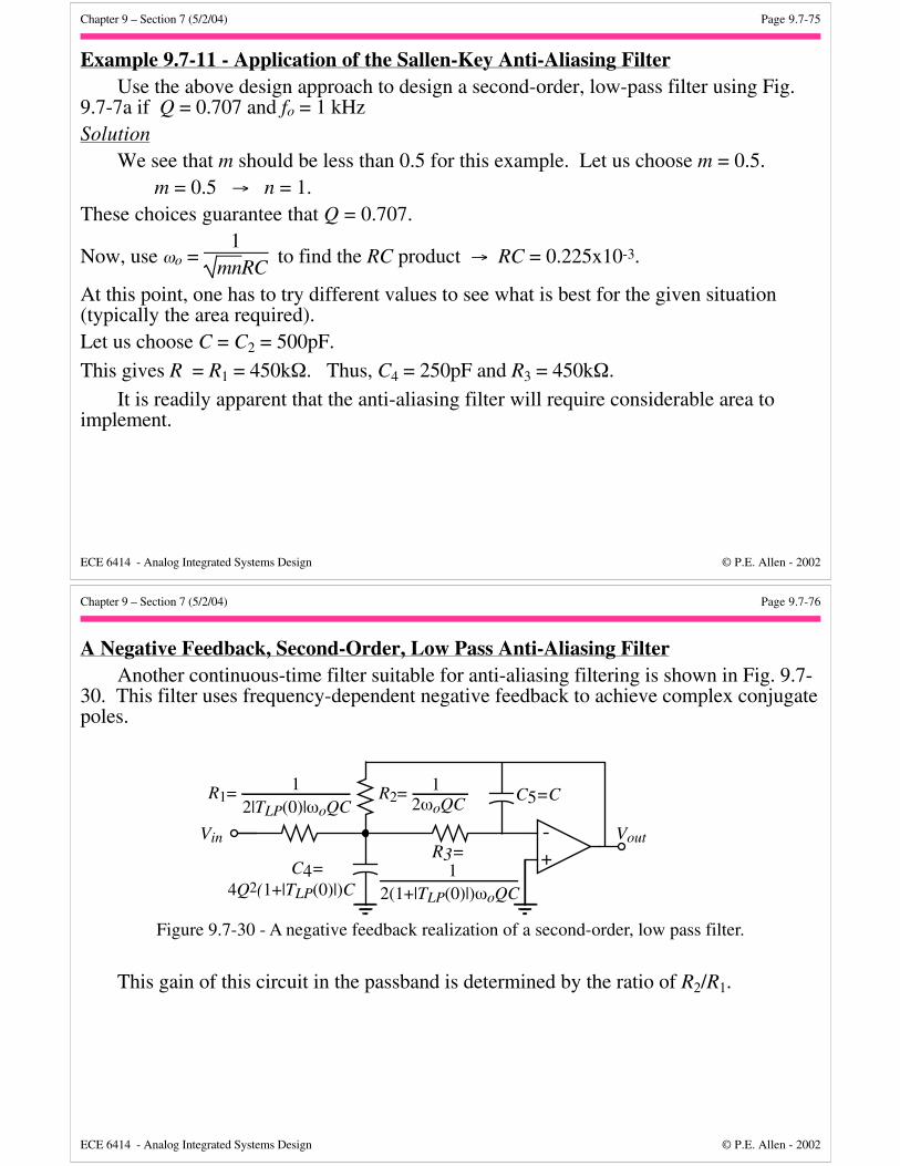
Chapter 9 – Section 7 (5/2/04) Page 9.7-75
ECE 6414 - Analog Integrated Systems Design © P.E. Allen - 2002
Example 9.7-11 - Application of the Sallen-Key Anti-Aliasing Filter Use the above design approach to design a second-order, low-pass filter using Fig.9.7-7a if Q = 0.707 and fo = 1 kHzSolution
We see that m should be less than 0.5 for this example. Let us choose m = 0.5.m = 0.5 → n = 1.
These choices guarantee that Q = 0.707.
Now, use ωo = 1
mnRC to find the RC product → RC = 0.225x10⁻³.
At this point, one has to try different values to see what is best for the given situation(typically the area required).Let us choose C = C2 = 500pF.
This gives R = R1 = 450kΩ. Thus, C4 = 250pF and R3 = 450kΩ.
It is readily apparent that the anti-aliasing filter will require considerable area toimplement.
Chapter 9 – Section 7 (5/2/04) Page 9.7-76
ECE 6414 - Analog Integrated Systems Design © P.E. Allen - 2002
A Negative Feedback, Second-Order, Low Pass Anti-Aliasing FilterAnother continuous-time filter suitable for anti-aliasing filtering is shown in Fig. 9.7-
30. This filter uses frequency-dependent negative feedback to achieve complex conjugatepoles.
+-
C5=C
C4=4Q2(1+|TLP(0)|)C
R1= 12|TLP(0)|ωoQC
R2= 12ωoQC
R3=1
2(1+|TLP(0)|)ωoQC
Vin Vout
Figure 9.7-30 - A negative feedback realization of a second-order, low pass filter.
This gain of this circuit in the passband is determined by the ratio of R2/R1.
Chapter 9 – Section 7 (5/2/04) Page 9.7-77
ECE 6414 - Analog Integrated Systems Design © P.E. Allen - 2002
Example 9.7-12 - Design of A Negative Feedback, Second-Order, Low-Pass ActiveFilter
Use the negative feedback, second-order, low-pass active filter of Fig. 9.7-30 todesign a low-pass filter having a dc gain of -1, Q = 1/ 2 , and fo = 10kHz.Solution
Let us use the design equations given on Fig. 9.7-30. Assume that C5 = C = 100pF.Therefore, we get C4 = (8)(0.5)C = 400pF. The resistors are
R1 = 2
(2)(1)(6.2832)(10-6) = 112.54 kΩ
R2 = 2
(2)(6.2832)(10-6) = 112.54 kΩ
and
R3 = 2
(2)(6.2832)(2)(10-6) = 56.27 kΩ
Unfortunately we see that again because of the passive element sizes that anti-aliasing filters will occupy a large portion of the chip.
Chapter 9 – Section 8 (5/2/04) Page 9.8-1
ECE 6414 - Analog Integrated Systems Design © P.E. Allen - 2002
SUMMARY• Switched capacitor circuits have reached maturity in CMOS technology.• The switched capacitor circuit concept was a pivotal step in the implementation of
analog signal processing circuits in CMOS technology.• The accuracy of the signal processing is proportional to the capacitor ratios.• Switched capacitor circuits have been developed for:
AmplificationIntegrationDifferentiationSummationFilteringComparisonAnalog-digital conversion
• Approaches to switched capacitor circuit design:Oversampled approach – clock frequency is much greater than the signal frequencyz-domain approach – the specifications are converted to the z-domain and directly
realized. Such circuits can operate to within half of the clock frequency.• SPICE or SWITCAP permits frequency domain simulation of switched capacitor ckts.• Clock feedthrough and kT/C noise represent the lower limit of the dynamic range of
switched capacitor circuits.