Embed Size (px)
Citation preview
Assoc.Prof.ThamerM.JamelElectronicIFirstClass
1
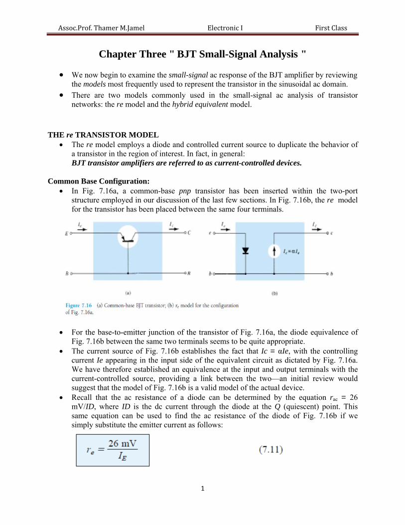
Chapter Three " BJT Small-Signal Analysis "
We now begin to examine the small-signal ac response of the BJT amplifier by reviewing the models most frequently used to represent the transistor in the sinusoidal ac domain.
There are two models commonly used in the small-signal ac analysis of transistor networks: the re model and the hybrid equivalent model.
THE re TRANSISTOR MODEL
The re model employs a diode and controlled current source to duplicate the behavior of a transistor in the region of interest. In fact, in general: BJT transistor amplifiers are referred to as current-controlled devices.
Common Base Configuration:
In Fig. 7.16a, a common-base pnp transistor has been inserted within the two-port structure employed in our discussion of the last few sections. In Fig. 7.16b, the re model for the transistor has been placed between the same four terminals.
For the base-to-emitter junction of the transistor of Fig. 7.16a, the diode equivalence of
Fig. 7.16b between the same two terminals seems to be quite appropriate. The current source of Fig. 7.16b establishes the fact that Ic = αIe, with the controlling
current Ie appearing in the input side of the equivalent circuit as dictated by Fig. 7.16a. We have therefore established an equivalence at the input and output terminals with the current-controlled source, providing a link between the two—an initial review would suggest that the model of Fig. 7.16b is a valid model of the actual device.
Recall that the ac resistance of a diode can be determined by the equation rac = 26 mV/ID, where ID is the dc current through the diode at the Q (quiescent) point. This same equation can be used to find the ac resistance of the diode of Fig. 7.16b if we simply substitute the emitter current as follows:
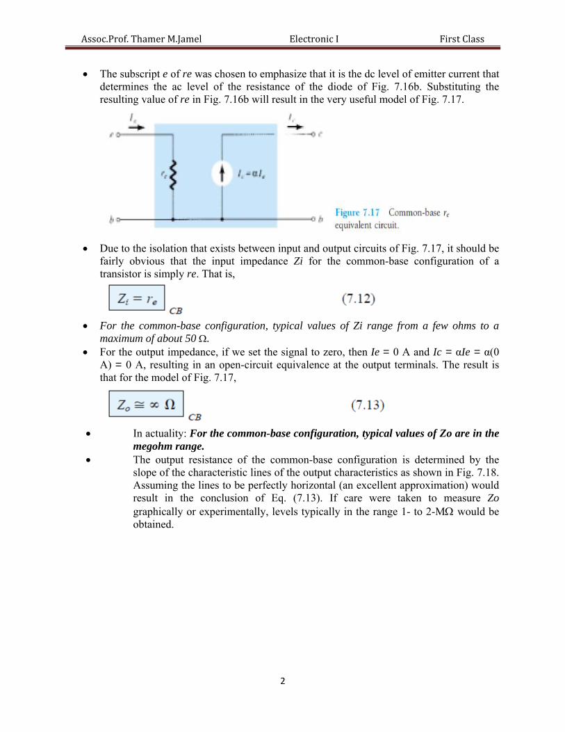
Assoc.Prof.ThamerM.JamelElectronicIFirstClass
2
The subscript e of re was chosen to emphasize that it is the dc level of emitter current that determines the ac level of the resistance of the diode of Fig. 7.16b. Substituting the resulting value of re in Fig. 7.16b will result in the very useful model of Fig. 7.17.
Due to the isolation that exists between input and output circuits of Fig. 7.17, it should be
fairly obvious that the input impedance Zi for the common-base configuration of a transistor is simply re. That is,
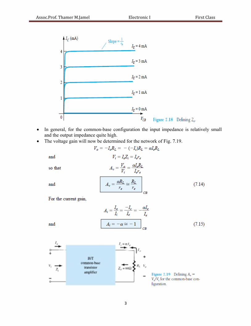
For the common-base configuration, typical values of Zi range from a few ohms to a
maximum of about 50 . For the output impedance, if we set the signal to zero, then Ie = 0 A and Ic = αIe = α(0
A) = 0 A, resulting in an open-circuit equivalence at the output terminals. The result is that for the model of Fig. 7.17,
In actuality: For the common-base configuration, typical values of Zo are in the
megohm range. The output resistance of the common-base configuration is determined by the
slope of the characteristic lines of the output characteristics as shown in Fig. 7.18. Assuming the lines to be perfectly horizontal (an excellent approximation) would result in the conclusion of Eq. (7.13). If care were taken to measure Zo graphically or experimentally, levels typically in the range 1- to 2-M would be obtained.
Assoc.Prof.ThamerM.JamelElectronicIFirstClass
3
In general, for the common-base configuration the input impedance is relatively small
and the output impedance quite high. The voltage gain will now be determined for the network of Fig. 7.19.
Assoc.Prof.ThamerM.JamelElectronicIFirstClass
4
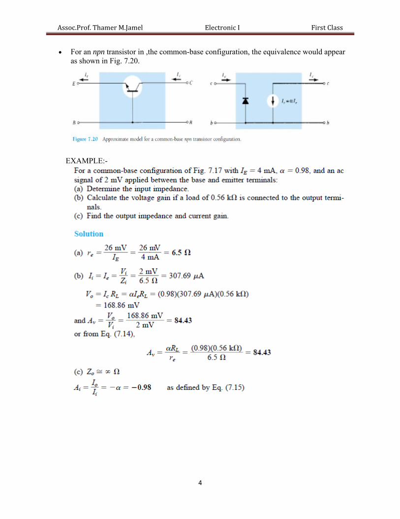
For an npn transistor in ,the common-base configuration, the equivalence would appear as shown in Fig. 7.20.
EXAMPLE:-
Assoc.Prof.ThamerM.JamelElectronicIFirstClass
5
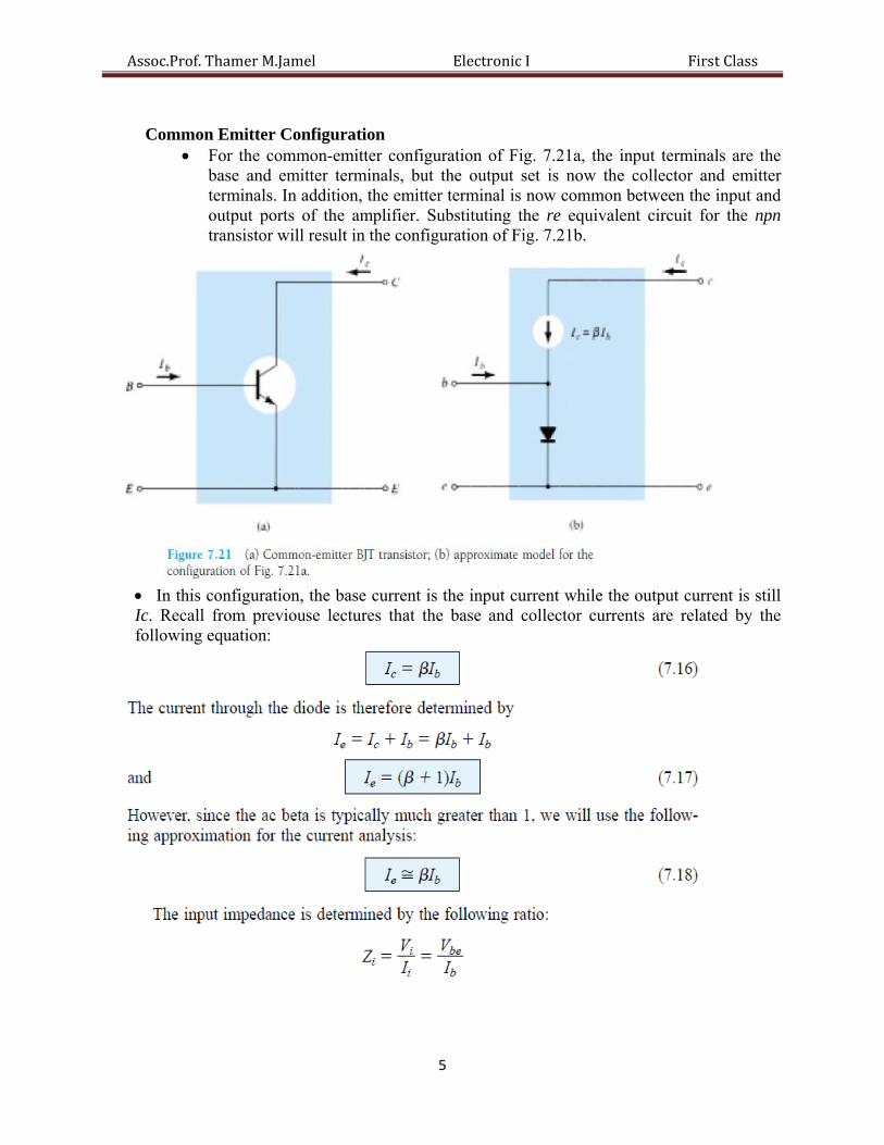
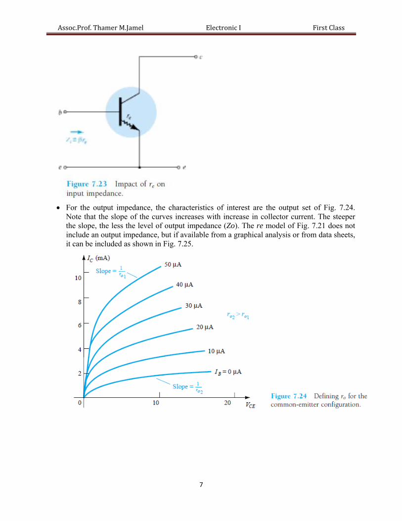
Common Emitter Configuration
For the common-emitter configuration of Fig. 7.21a, the input terminals are the base and emitter terminals, but the output set is now the collector and emitter terminals. In addition, the emitter terminal is now common between the input and output ports of the amplifier. Substituting the re equivalent circuit for the npn transistor will result in the configuration of Fig. 7.21b.
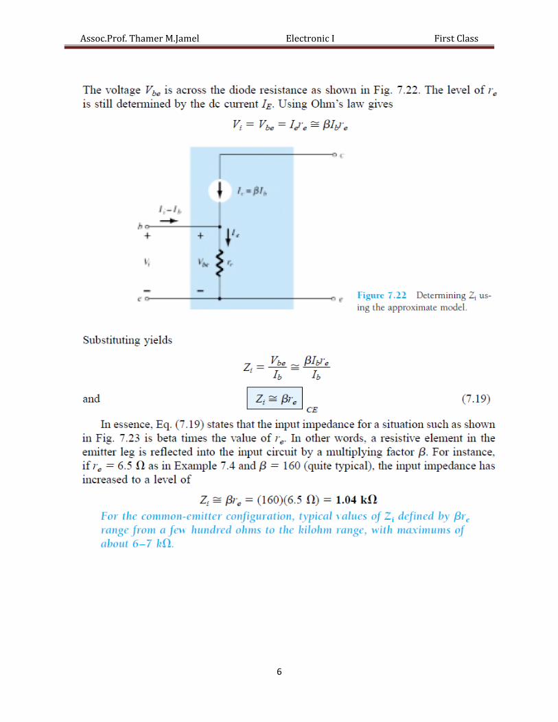
In this configuration, the base current is the input current while the output current is still Ic. Recall from previouse lectures that the base and collector currents are related by the following equation:
Assoc.Prof.ThamerM.JamelElectronicIFirstClass
6
Assoc.Prof.ThamerM.JamelElectronicIFirstClass
7
For the output impedance, the characteristics of interest are the output set of Fig. 7.24.
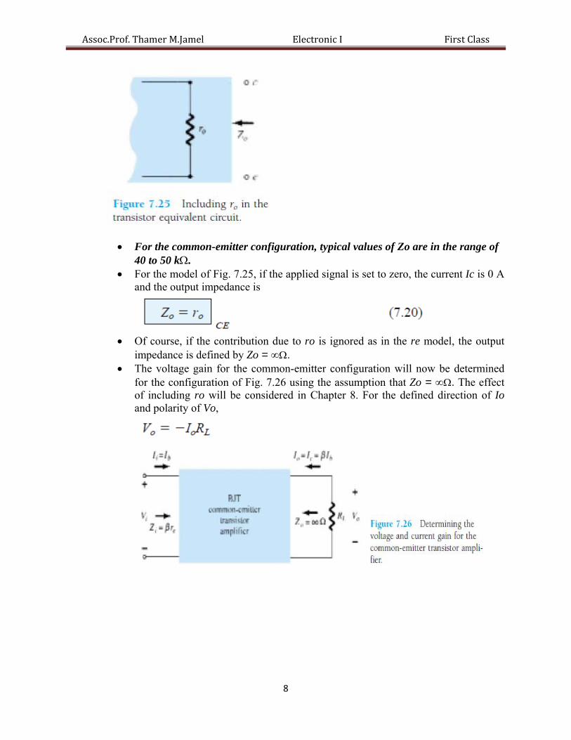
Note that the slope of the curves increases with increase in collector current. The steeper the slope, the less the level of output impedance (Zo). The re model of Fig. 7.21 does not include an output impedance, but if available from a graphical analysis or from data sheets, it can be included as shown in Fig. 7.25.
Assoc.Prof.ThamerM.JamelElectronicIFirstClass
8
For the common-emitter configuration, typical values of Zo are in the range of
40 to 50 k. For the model of Fig. 7.25, if the applied signal is set to zero, the current Ic is 0 A
and the output impedance is
Of course, if the contribution due to ro is ignored as in the re model, the output
impedance is defined by Zo = . The voltage gain for the common-emitter configuration will now be determined
for the configuration of Fig. 7.26 using the assumption that Zo = . The effect of including ro will be considered in Chapter 8. For the defined direction of Io and polarity of Vo,
Assoc.Prof.ThamerM.JamelElectronicIFirstClass
9
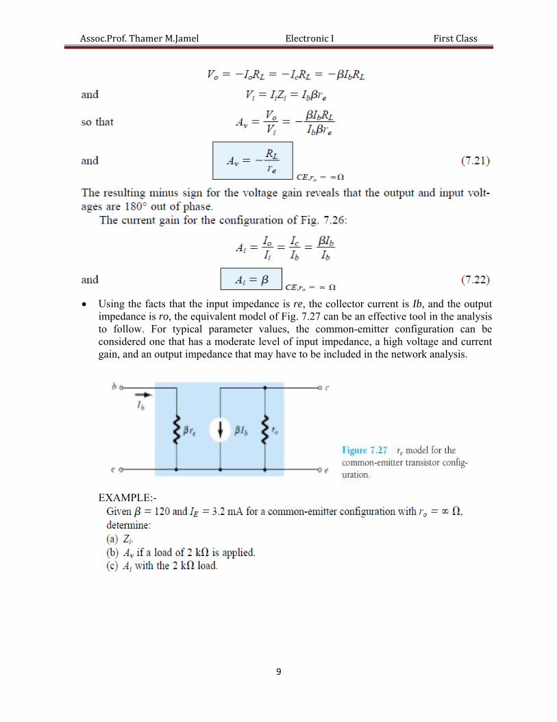
Using the facts that the input impedance is re, the collector current is Ib, and the output
impedance is ro, the equivalent model of Fig. 7.27 can be an effective tool in the analysis to follow. For typical parameter values, the common-emitter configuration can be considered one that has a moderate level of input impedance, a high voltage and current gain, and an output impedance that may have to be included in the network analysis.
EXAMPLE:-
Assoc.Prof.ThamerM.JamelElectronicIFirstClass
10
Common Collector Configuration For the common-collector configuration, the model defined for the common-emitter
configuration of Fig. 7.21 is normally applied rather than defining a model for the common-collector configuration.
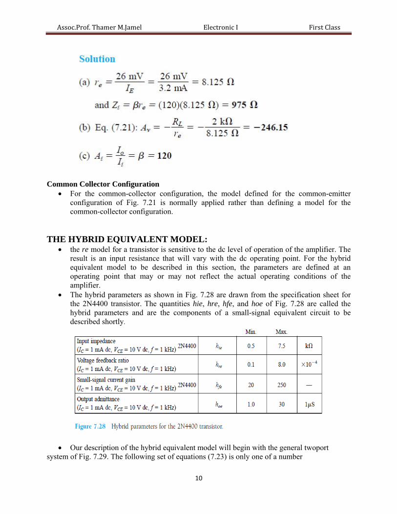
THE HYBRID EQUIVALENT MODEL: the re model for a transistor is sensitive to the dc level of operation of the amplifier. The
result is an input resistance that will vary with the dc operating point. For the hybrid equivalent model to be described in this section, the parameters are defined at an operating point that may or may not reflect the actual operating conditions of the amplifier.
The hybrid parameters as shown in Fig. 7.28 are drawn from the specification sheet for the 2N4400 transistor. The quantities hie, hre, hfe, and hoe of Fig. 7.28 are called the hybrid parameters and are the components of a small-signal equivalent circuit to be described shortly.
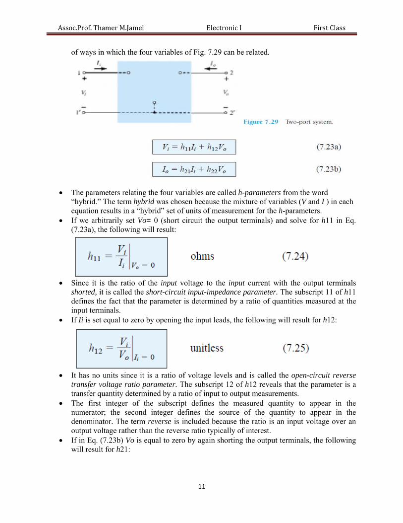
Our description of the hybrid equivalent model will begin with the general twoport system of Fig. 7.29. The following set of equations (7.23) is only one of a number
Assoc.Prof.ThamerM.JamelElectronicIFirstClass
11
of ways in which the four variables of Fig. 7.29 can be related.
The parameters relating the four variables are called h-parameters from the word
“hybrid.” The term hybrid was chosen because the mixture of variables (V and I ) in each equation results in a “hybrid” set of units of measurement for the h-parameters.
If we arbitrarily set Vo= 0 (short circuit the output terminals) and solve for h11 in Eq. (7.23a), the following will result:
Since it is the ratio of the input voltage to the input current with the output terminals
shorted, it is called the short-circuit input-impedance parameter. The subscript 11 of h11 defines the fact that the parameter is determined by a ratio of quantities measured at the input terminals.
If Ii is set equal to zero by opening the input leads, the following will result for h12:
It has no units since it is a ratio of voltage levels and is called the open-circuit reverse
transfer voltage ratio parameter. The subscript 12 of h12 reveals that the parameter is a transfer quantity determined by a ratio of input to output measurements.
The first integer of the subscript defines the measured quantity to appear in the numerator; the second integer defines the source of the quantity to appear in the denominator. The term reverse is included because the ratio is an input voltage over an output voltage rather than the reverse ratio typically of interest.
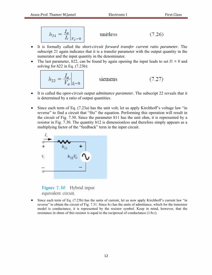
If in Eq. (7.23b) Vo is equal to zero by again shorting the output terminals, the following will result for h21:
Assoc.Prof.ThamerM.JamelElectronicIFirstClass
12
It is formally called the short-circuit forward transfer current ratio parameter. The
subscript 21 again indicates that it is a transfer parameter with the output quantity in the numerator and the input quantity in the denominator.
The last parameter, h22, can be found by again opening the input leads to set I1 = 0 and solving for h22 in Eq. (7.23b):
It is called the open-circuit output admittance parameter. The subscript 22 reveals that it
is determined by a ratio of output quantities.
Since each term of Eq. (7.23a) has the unit volt, let us apply Kirchhoff’s voltage law “in reverse” to find a circuit that “fits” the equation. Performing this operation will result in the circuit of Fig. 7.30. Since the parameter h11 has the unit ohm, it is represented by a resistor in Fig. 7.30. The quantity h12 is dimensionless and therefore simply appears as a multiplying factor of the “feedback” term in the input circuit.
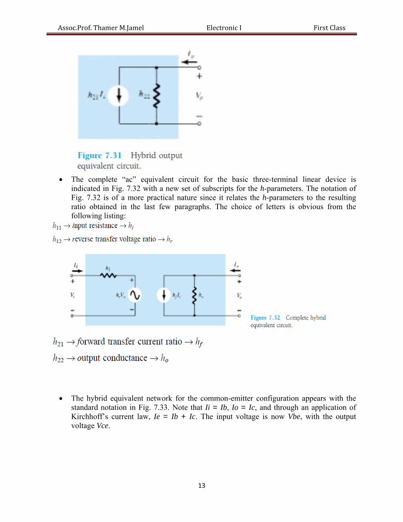
Since each term of Eq. (7.23b) has the units of current, let us now apply Kirchhoff’s current law “in
reverse” to obtain the circuit of Fig. 7.31. Since h22 has the units of admittance, which for the transistor model is conductance, it is represented by the resistor symbol. Keep in mind, however, that the resistance in ohms of this resistor is equal to the reciprocal of conductance (1/h22).
Assoc.Prof.ThamerM.JamelElectronicIFirstClass
13
The complete “ac” equivalent circuit for the basic three-terminal linear device is
indicated in Fig. 7.32 with a new set of subscripts for the h-parameters. The notation of Fig. 7.32 is of a more practical nature since it relates the h-parameters to the resulting ratio obtained in the last few paragraphs. The choice of letters is obvious from the following listing:
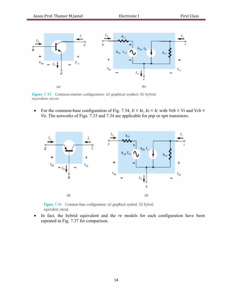
The hybrid equivalent network for the common-emitter configuration appears with the
standard notation in Fig. 7.33. Note that Ii = Ib, Io = Ic, and through an application of Kirchhoff’s current law, Ie = Ib + Ic. The input voltage is now Vbe, with the output voltage Vce.
Assoc.Prof.ThamerM.JamelElectronicIFirstClass
14
For the common-base configuration of Fig. 7.34, Ii = Ie, Io = Ic with Veb = Vi and Vcb = Vo. The networks of Figs. 7.33 and 7.34 are applicable for pnp or npn transistors.
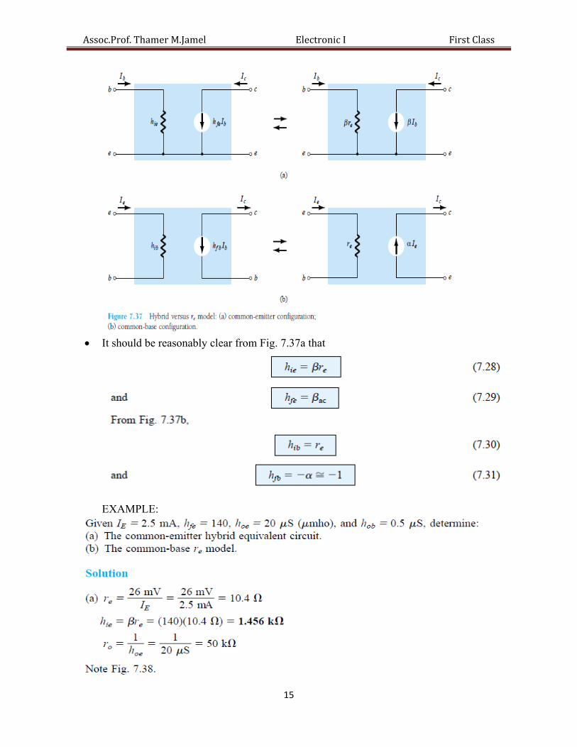
In fact, the hybrid equivalent and the re models for each configuration have been
repeated in Fig. 7.37 for comparison.
Assoc.Prof.ThamerM.JamelElectronicIFirstClass
15
It should be reasonably clear from Fig. 7.37a that
EXAMPLE:
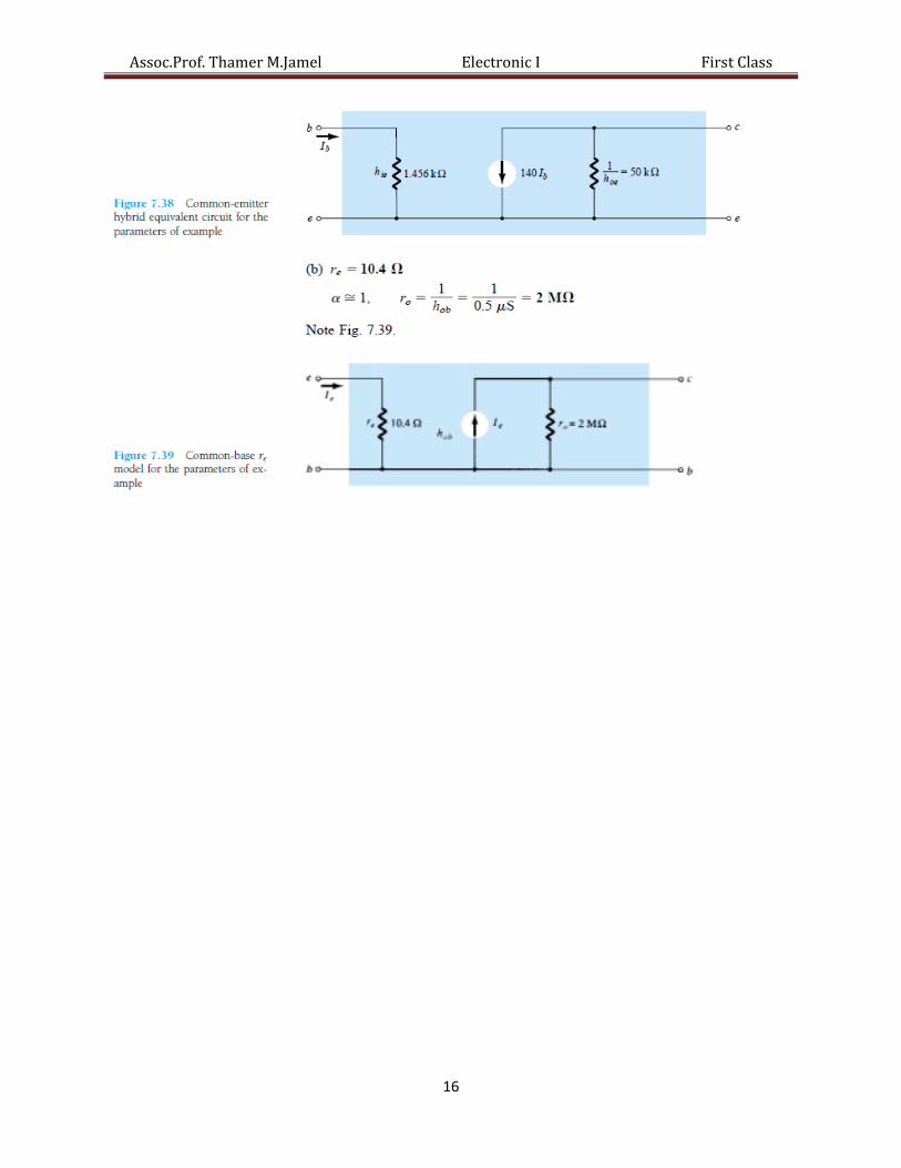
Assoc.Prof.ThamerM.JamelElectronicIFirstClass
16
Assoc.Prof.ThamerM.JamelElectronicIFirstClass
17
BJT small signal ac analysis
The transistor models introduced previously will now be used to perform a small signal ac analysis of a number of standard transistor network configurations.
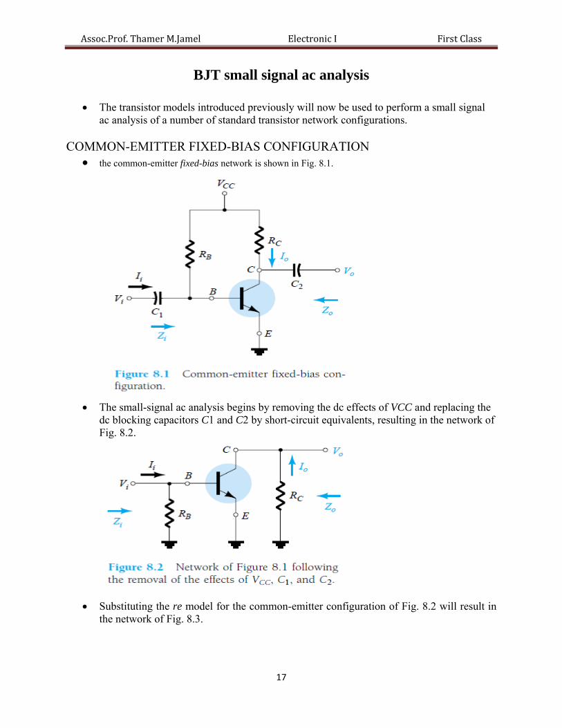
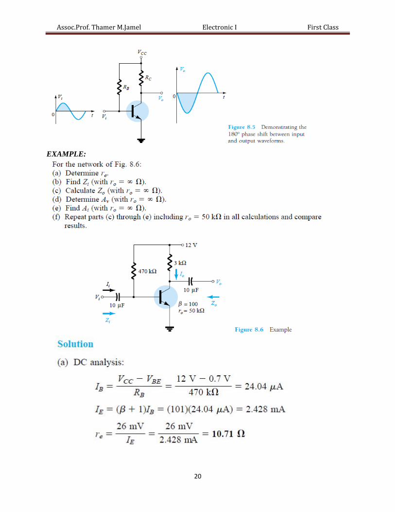
COMMON-EMITTER FIXED-BIAS CONFIGURATION the common-emitter fixed-bias network is shown in Fig. 8.1.
The small-signal ac analysis begins by removing the dc effects of VCC and replacing the
dc blocking capacitors C1 and C2 by short-circuit equivalents, resulting in the network of Fig. 8.2.
Substituting the re model for the common-emitter configuration of Fig. 8.2 will result in
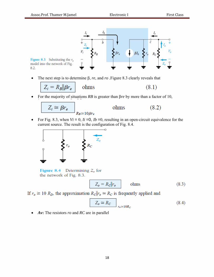
the network of Fig. 8.3.
Assoc.Prof.ThamerM.JamelElectronicIFirstClass
18
The next step is to determine β, re, and ro .Figure 8.3 clearly reveals that
For the majority of situations RB is greater than βre by more than a factor of 10,
For Fig. 8.3, when Vi = 0, Ii =0, Ib =0, resulting in an open-circuit equivalence for the
current source. The result is the configuration of Fig. 8.4.
Av: The resistors ro and RC are in parallel
Assoc.Prof.ThamerM.JamelElectronicIFirstClass
19
Ai: The current gain is determined in the following manner: Applying the current- divider
rule to the input and output circuits,
Phase Relationship: The negative sign in the resulting equation for Av reveals that a
180° phase shift occurs between the input and output signals, as shown in Fig.8.5.
Assoc.Prof.ThamerM.JamelElectronicIFirstClass
20
EXAMPLE:
Assoc.Prof.ThamerM.JamelElectronicIFirstClass
21
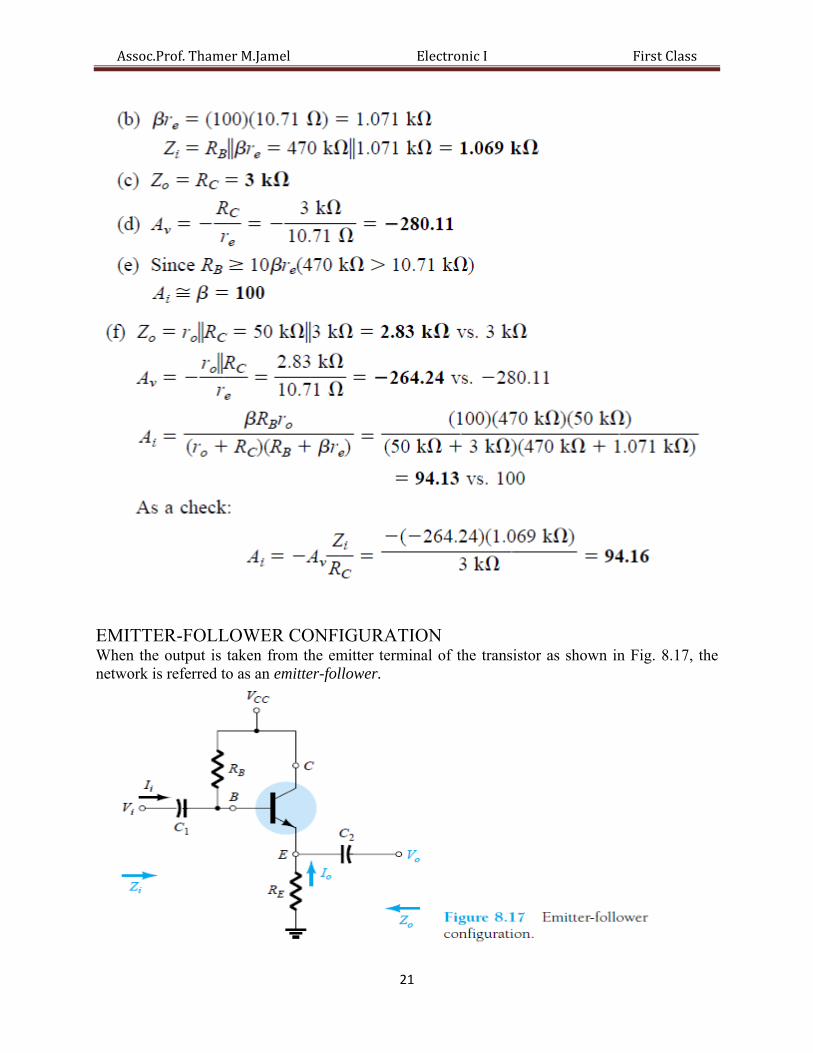
EMITTER-FOLLOWER CONFIGURATION When the output is taken from the emitter terminal of the transistor as shown in Fig. 8.17, the network is referred to as an emitter-follower.
Assoc.Prof.ThamerM.JamelElectronicIFirstClass
22
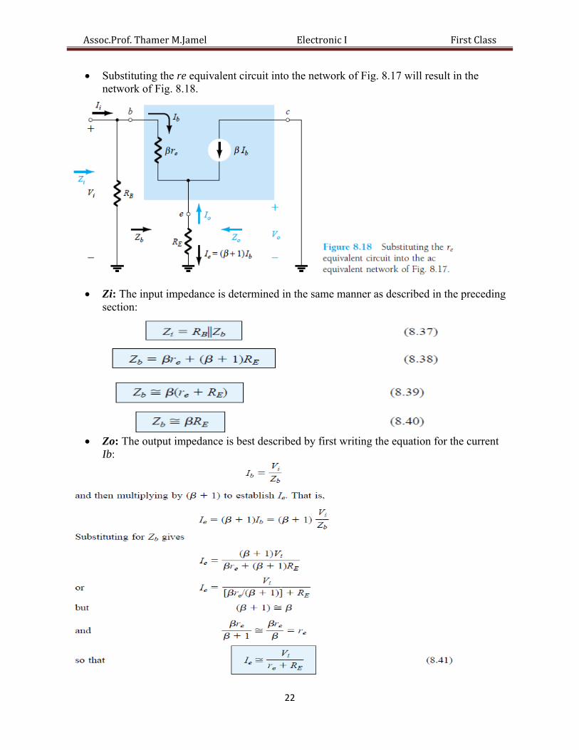
Substituting the re equivalent circuit into the network of Fig. 8.17 will result in the network of Fig. 8.18.
Zi: The input impedance is determined in the same manner as described in the preceding
section:
Zo: The output impedance is best described by first writing the equation for the current
Ib:
Assoc.Prof.ThamerM.JamelElectronicIFirstClass
23
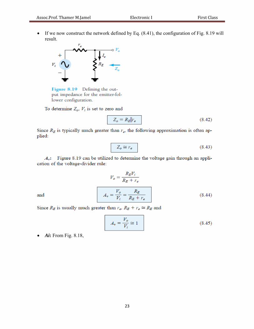
If we now construct the network defined by Eq. (8.41), the configuration of Fig. 8.19 will result.
Ai: From Fig. 8.18,
Assoc.Prof.ThamerM.JamelElectronicIFirstClass
24
Phase relationship: As revealed by Eq. (8.44) and earlier discussions of this section, Vo
and Vi are in phase for the emitter-follower configuration. Effect of ro:
Zi:
Assoc.Prof.ThamerM.JamelElectronicIFirstClass
25
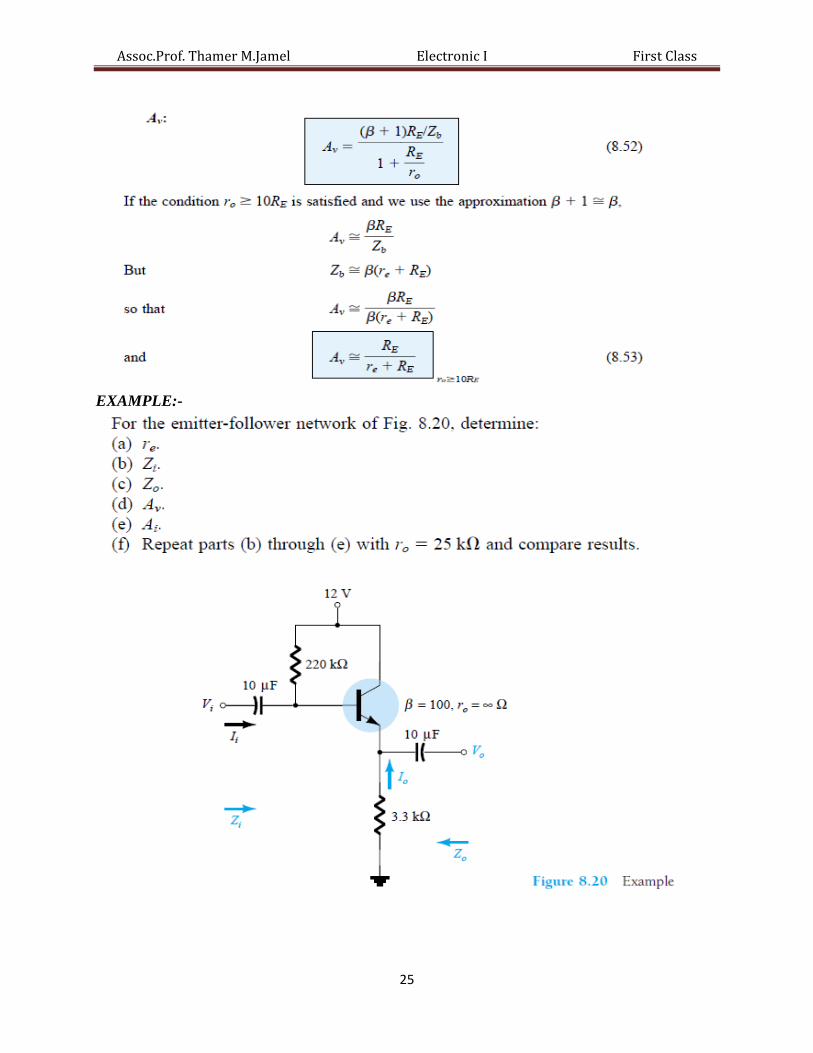
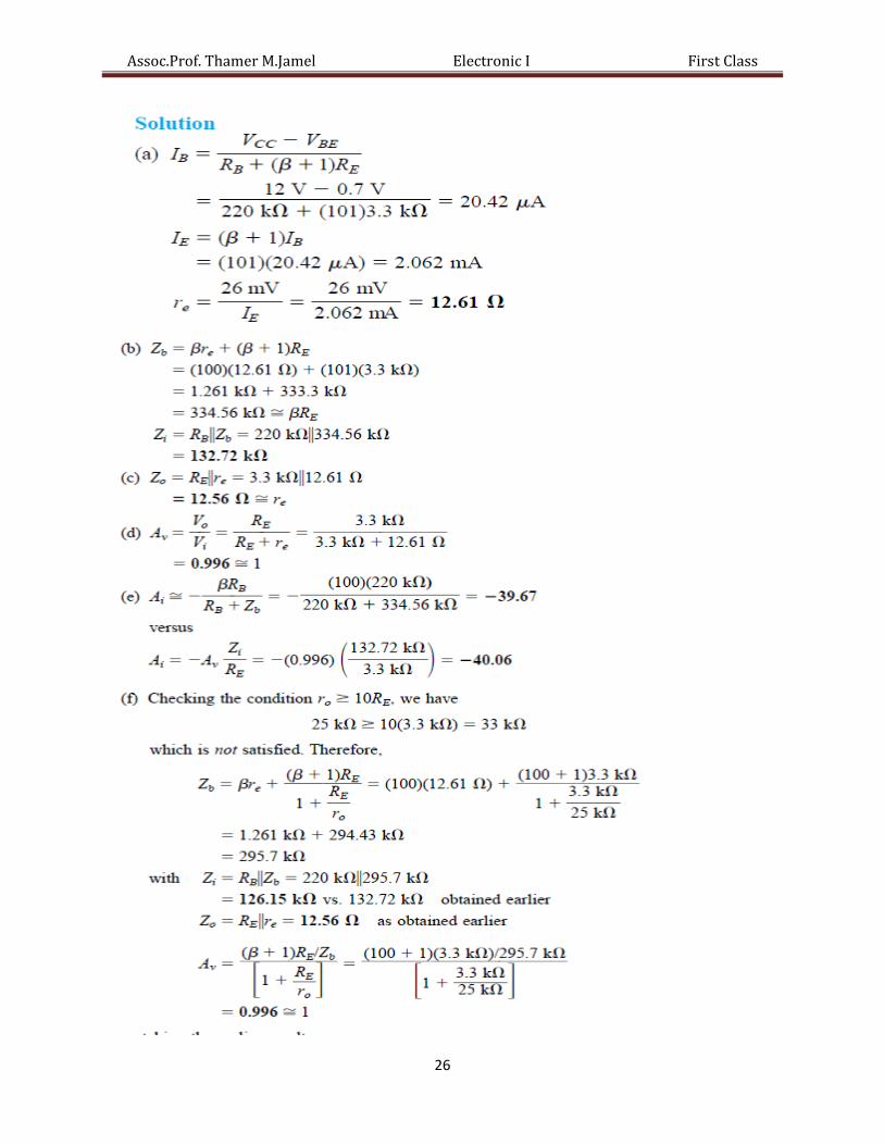
EXAMPLE:-
Assoc.Prof.ThamerM.JamelElectronicIFirstClass
26
Assoc.Prof.ThamerM.JamelElectronicIFirstClass
27
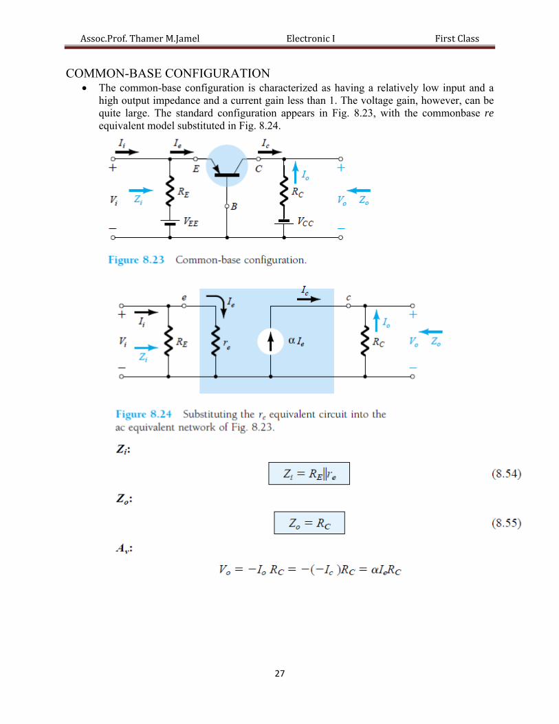
COMMON-BASE CONFIGURATION The common-base configuration is characterized as having a relatively low input and a
high output impedance and a current gain less than 1. The voltage gain, however, can be quite large. The standard configuration appears in Fig. 8.23, with the commonbase re equivalent model substituted in Fig. 8.24.
Assoc.Prof.ThamerM.JamelElectronicIFirstClass
28
Phase relationship: The fact that Av is a positive number reveals that Vo and Vi are in phase for the common-base configuration.
Effect of ro: For the common-base configuration, ro = 1/hob is typically in the megohm range and sufficiently larger than the parallel resistance RC to permit the approximation
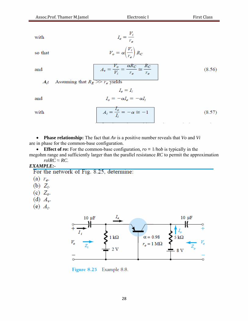
roǁRC ≈ RC. EXAMPLE:-
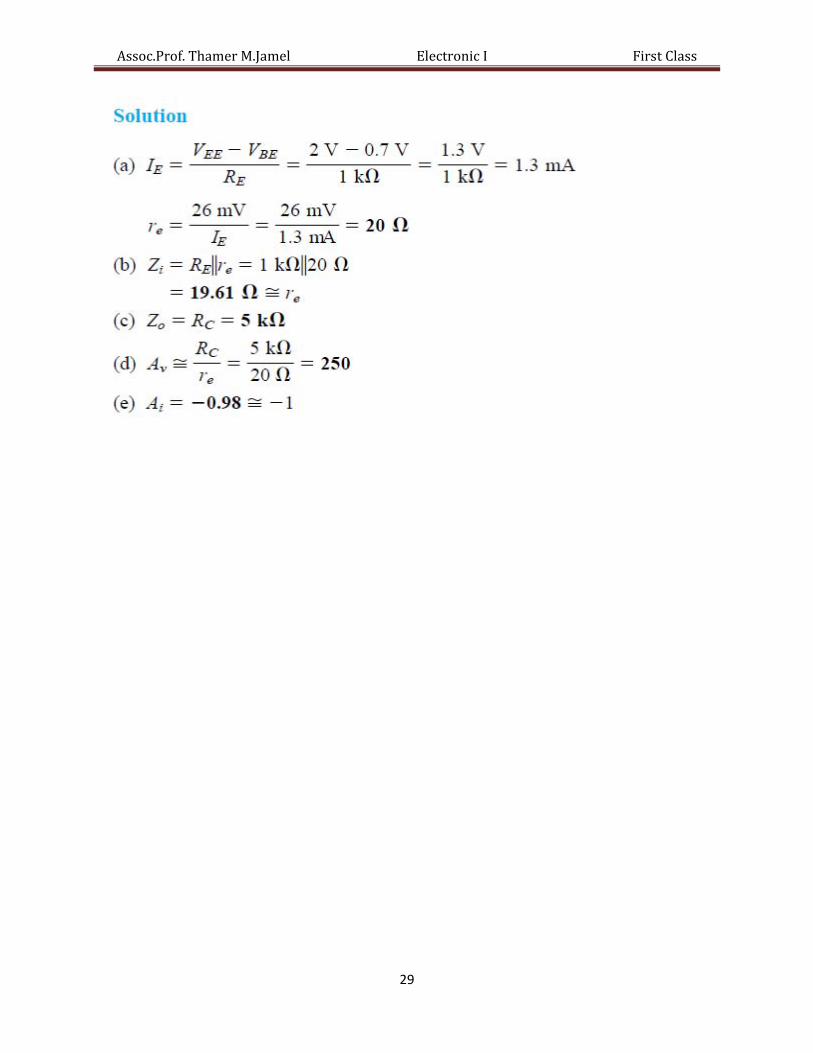
Assoc.Prof.ThamerM.JamelElectronicIFirstClass
29