Embed Size (px)
Citation preview

Chapter 3
Characterisation of Zinc Tin
Oxide Thin Films Prepared
by Pulsed Laser Deposition
This ch'tpter describes the preparation of zinc tin oxide (ZTO) thin films
by pulsed laser deposition (PLD) technique and their optical and electrical
characterisations.
3.1 Introduction
Demands for visibly transparent and electrically conductive materials are
rapidly growing in technological applications in optoelectronic devices like
solar cells, liquid crystal displays, energy efficient windows and 'invisible
electronic circuits' etc. A few crystalline materials like tin doped indium
oxide (ITO) , aluminium doped zinc oxide (ZnO:AI) and antimony doped
tin oxide (Sn02:Sb) in thin film form are presently being used for such
129

130 Characterisation of ZTO Thin Films Prepared by PLD
applications. Zinc tin oxide films have the advantages of both ZnO (higher
transparency and more stability in activated hydrogen environments than
ITO and Sn02) and Sn02 (high stability in acidic and basic solutions and
in oxidizing environments at higher temperatures) [165-170]. Zinc tin ox
ide films have been grown by radio frequency and direct current magnetron
sputtering, filtered vacuum arc deposition etc [171-175]. Most of these
works were devoted to understand the optical and electrical properties of
polycrystalline films deposited either by suhstrat.e heating or by high tem
perature post deposition annealing.
Amorphous transparent conductors are much attractive because they
need a low processing temperature and can be grown on plastic substrates
to form high-quality films suitable for practical devices. Since the mobility
of conduction electrons is proportional to the width of the conduction bands
and a narrow band tends to localize carriers, a large overlap between rele
vant orbitals is required to achieve a large mobility degenerate conduction
in amorphous semiconductors. In addition, the magnitude of the orbital
overlap needs to be insensitive to the structural randomness, which is in
trinsic to the amorphous state, to reduce the formation of shallow localized
states (often referred to as tail states). ivIetal oxides composed of heavy
metal cations (HMCs) with an electronic configuration (n -l)dlOnsO (with
n ~ 4) satisfy these requirements. A large band gap in oxides is attained
by the low energy of oxygen 2p orbitals, which constitute the valence band
maximum region. The bottom part of the conduction band in these oxides
is primarily composed of ns orbitals of HMCs [59, 60].
Experimental conditions 131
3.2 Experimental conditions
Polycrystalline ceramic targets were prepared from a mixture of ZnO (99.999%
pure) and 8n02 (99.999% pure) powders (Zn:Sn = 1:1, 2:1, 4:1 and 8:1).
The mixed powders were initially calcined at 10000 e for 4 hours and then
hydrostatically pressed at a pressure of 1000 Kgcm-2 to form a pellet of
1 cm diameter. The pellets were then sintercd at 1450 °e for 6 hours. As
discussed later in this session, the target with composition Zn:Sn = 2:1
formed a single phase compound of Zn28n04, and the other composition
target lead to a mixture of ZnO, 8n02, and Zn28n04, which were con
firmed by XRD measurements (Figure 3.2). Thin films were deposited at
RT by PLD from ceramics targets of ZTO with a KrF excimer laser (248
nm wavelength, 10 Hz repetition frequency). Laser' ablation was carried
out at a laser energy density of 35 mJcm-2pulse- 1. Films were deposited
on glass substrates placed at a distance of 30 mm from the target. The de
positions were carried out for 30 minutes by varying oxygen pressure (P02)
from 0 to 9 Pa. The resulting film thicknesses varied from 110 - 200 nm.
To study the effects of post-deposition annealing on film properties, some
films were annealed at temperatures up to BOOae in air.
3.3 Chemical composition
Chemical composition of the targets and thin films were determined from
the XRF analysis. Figure 3.1 shows the compositional variation in the
films with P02 during deposition. It was confirmed that the Zn/8n ratios
of the sintered targets were the same as those of the corresponding starting
compositions (Inset of figure 3.1). Film composition shows some variation

132
2.0
1.5
§ ;;: - 1.0 0 0 ;: f! 0.5
c: Cl) "- 0.0 c: N
-0.5
-1.0
Characterisation of ZTO Thin Films Prepared by PLD
Target Zn:Sn = 2:1 e e_e__ ________
e_______. ________ e e
Target Zn:Sn = 1:1
;,~.,----------.------.------. • ~ 9,.---------------,
o
:l • ! 7 J!! 8 c; 5 .. "0 o ~ 2 c: ~ D~~_7~~~_7-~~_7~ c 0 3 4 5 6 N
StartIng 2"IS" ratio
2 4 6 8
Oxygen partial pressure (Pa)
10
Figure 3.1: ZnjSn compositional variations with respect to oxygen partial pres
sure for the PLD films deposited using different targets with the Zn:Sn ratios of
1:1 and 2:1. Inset shows the Zn/Sn composition in the sintered target.
with P02' but is more or less the same as that of the PLD target, indicating
that the PLD process can reproduce the chemical composition of the target
in the films if an appropriate deposition condition is chosen.
3.4 Structural characterisation
ZnO-Sn02 systems are reported to have two phases: Zn2Sn04 and ZnSn03
[176]. The Zn2Sn04 has a spinal type structure and has high thermal stabil
ity. The ZnSn03 exists in a stable crystalline form at temperatures < 600
°C and shows an ilmenite like structure. XRD patterns of the sintered tar
get.s are shown in figure 3.2. The target. with composition Zn:Sn = 2:1 forms

Structural characterisation 133
;=-
Zn2SnO. ~ Zn:Sn = 2:1
;=- 0 M - v UI ::!t- o> - ~
'2 :::J
.Q ....
.e * >- + ... 'iij
+Sn02 C
(I) • Zn
2SnO.
Zn:Sn = 1:1 - * .E + *
10 20 30 40 50 60 70 81
26 (degree)
Figure 3.2: XRD pattern of PLD targets with the Zn:Sn ratios of 1:1 and 2:l.
The Zn:Sn = 2:1 targct forms a single phase compound of Zn2Sn04. In the lower
figure, * denotcs Zn2Sn04 and + denotes Sn02.
a single phase compound of Zn28n04, and the other composition lead to a
mixture of ZnO, Sn02, and Zn28n04' It has been reported that crystalline
Zn8n03 cannot be prepared under calcination temperature> 700°C [177].
The only stable phases at high temperature (> 1000 °C) in the ZnO-8n02
system are Zn28n04, ZnO and 8n02 [176]. As the Zn content in the target
is increased, the ZnO phase in the target becomes more and more promi
nent as observed from the increased intensity of diffraction peaks from ZnO
planes. For films, glancing angle XRD analysis were performed at an inci
dent angle of 0.5°. As evident from the GXRD pattern of films, all films
were amorphous irrespective of the variations in oxygen partial pressure
(Figure 3.3). Figure 3.4 show GXRD patterns of the films deposited using

134 Characterisation of ZTO Thin Films Prepared by PLD
Zn:Sn=l:l
7.0 Pa
en 5.0 Pa ,~ c :l
.Q 2.0 Pa ....
.!!. ~ 1.0 Pa 'iij c CII -E 0.5 Pa
o Pa
10 20 30 40 SO 60 70
2e {degree}
~ - Zn:Sn=2:1 9.0 Pa
~ 7.0 Pa "-
"- 5.0 Pa .......
i'--. 2.0Pa .......
i '- 1.0 Pa
"-- 0.5 Pa
~ -......... o Pa
10 20 30 40 50 60 70 80
29 (degree)
Figure 3,3: GXRD pattern of ZTO thin films prepared from targets with Zn:Sn
ratios of 1:1 and 2:1 at different oxygen partial prcssurcs.
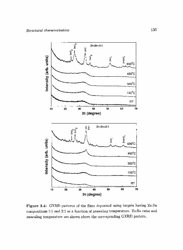
Structural characterisation 135
Goo'e
450'e
3000e
150'C
RT
10 20 30 40 50 60 70
29 (degree)
'11 Zn:Sn:::2:1 N
10 20 30 40 50 60 70
29 (degree)
Figure 3.4: GXRD patterns of the films deposited using targets having Zn:Sn
compositions 1:1 and 2:1 as a function of annealing temperature. Zn:Sn ratio and
annealing temperature are shown above the corresponding GXRD pattern.

136
.-. en -'c :::J
.e
.!.. ~ 'iij c CD -.5
10 20
Characterisation of ZTO Thin Films Prepared by PLD
30
o~ c:
(f)
rG
40 50
29 (degree)
60
ON Zn:Sn=2:1 c:
(f)
o~ c: (f)
rG
Zn:Sn::1:1
70 80
Figure 3.5: GXRD patterns of the films deposited from targets having Zn:Sn
compositions 1:1 and 2:1 after annealing at 800°C.
PLD targets with the Zn:Sn ratios of 1:1 and 2:1 as a function of post an
nealing temperature. It shows that the deposited films are amorphous, but
450°C annealing crystallizes the films partially to give crystalline phases
of the simple oxides, ZnO and 8n02. The halos around 2(J = 33° indicate
that some or large portion of the amorphous phases still remain. This result
should be compared with the results on films grown by sputtering in refer
ences [110] and [173], in which the former reported no crystallization up to
600°C while the latter reported the crystallization temperature as ",600
°C. The low crystallisation temperature in the present PLD grown films
would be attributed to the different growth kinetics of the films between
PLD and sputtering, where in general, deposition precursors have larger ki-

Structural characterisation 137
netic energies for PLD owing to the excitation hy high energy laser pulses
and few collisions of the deposition precursors with gaseous molecules due
to a lower P02 deposition condition. That is, it is speculated that higher
energy precursors in PLD deposition form a more relaxed amorphous struc
ture that is more easily crystallized. Further higher temperature annealing
at 600 - 800°C (Figure 3.5) eliminates the remaining amorpholls phases,
producing a new crystalline phase ZnSn03 as a consequence of solid state
reactions between the ZnO and Sn02 phases segregated at 450 - 600°C
and the remained amorphous ZTO film [176, 178].
Figure 3.6 shows the AFM images and root-mean-squares (rms) surface
roughness of the as-deposited films as a function of the chemical compo
sition and Po2 • It shows that the sllrface roughness depends on both the
chemical composition and P02 and ranges up to 11 nm. The films with
the Zn:Sn composition 1:1 have larger roughness compared to the 2:1 com
position films, and its roughness decreases with the increase of Po2 • The
films deposited from the Zn:Sn = 2:1 target have atomically flat surfaces
with surface roughness less than 0.3 nm at low P02 ~ 2Pa. For TFT
applications, an applied gate bias modulates the conductance of the semi
conductor layer and form an accumulated channel of carriers in a narrow
region confined at the semiconductor-insulator interface. Hence the surface
flatness of an active layer is an important parameter because carrier trans
port in TFT channels is significantly affected by the carrier scattering due
to roughness at the channel - gate insulator interface [179). Smoother the
interface, better will be the mobility of the carriers in the channel.
Figure 3.7 shows the AFM images of the film deposited from Zn:Sn
= 2: 1 target at an oxygen partial pressure of 0.5 Pa as a function of an
nealing temperature. The roughness of the film increases as the films are

138 Characterisation of ZTO Tltin Films Prepared by PLD
" r-----------------------------~ ,.
Figure 3.6: AFM images of ZTO films prepared from target composition (a)
Zn:Sn=1:1 and (b) Zn:Sn=2:1. Both films are deposited at room temperature
at an oxygen pressure of 0.5 Pa.(c) Dependence of surface roughness on oxygen
partial pressure for the films deposited from targets having Zn:Sn compOLSitioos
1:1 and 2:1.

Structural characterisation 139
Figure 3.7: AF!\! images of ZTO films deposited from Zn:Sn = 2:1 target At an
oxygen partial pressure of 0.5 Pa Ilnd t.hen annealed at. different temperatures.

140 Characterisa.tion of ZTO Thin Films Prepared by PLD
annealed at higher temperatures. As the films are annealed at higher tem
peratures, it crystallizes into different phases (ref.;r figure 3.4). The higher
film surface roughness at higher annealing temperatures is due to the facet
formation. The smoother surfaces of amorphous films change to granular
rough structures on annealing.
3.5 Optical properties
Figure 3.8 shows transmittance and reflectance spectra of the ZTO films
deposited at a P02 of 0.5 Pa. It shows that the ZTO films have average
transmittances> 85% in the visible region and significant difference is not
observed for the films having different chemical compositions.
The optical data in figure 3.8 were used in the Tauc plot to obtain
the bandgap value [Figures 3.9(a,b)J, which derived Efl values 2.37 - 2.86
eV varying with P02 as summarised in figure 3.9(c) (Method of bandgap
evaluation is given in section 2.2.5). There was some uncertainty in the
estimation of Ey at low P02 due to the presence of subgap states. The value
of Eg is insensitive to POl at P02 ? 2Pa. It should be noticed that the
fundamental band gap is an intrinsic property of a material: however, the
exceptionally small values are obtained for films grown at low Po2 , because
strong subgap absorption bands appear beneath the fundamental bandgap
and superimpose with the fundamental band absorption as observed in
figure 3.10. These results should also be compared with previously reported
results. As summarized in introduction of reference [110J and reported in
reference [173J, the Tauc gaps of ZTO films are 3.35 - 3.89 eV. But those
films were crystallized, and therefore they should not be compared with the

Optical properties 141
..-~ ~ I: 7S 0 :;: U Cl) ;: Cl)
50 a: C 0 .iij
.!!! E 25 /11 I: co ... I-
0 0 500 1000 1500 2000 2500
Wavelength (nm)
Figure 3.8: Optical transmission and reflection spectra of the ZTO films prepared
at Po, = 0.5 Pa from targets having Zn:Sn compositions 1:1 and 2:l. The films
are highly transparent across the visible region.
present data for amorphous ZTO. It indicates that the fundamental optical
gaps of ZTO films are reduced to 2.8 - 2.86 eV on amorphization.
Figures in 3.10 are log( 0:) - hv plots that show subgap absorption more
clearl:y. It is observed that the as-deposited films P02 ::; 2 Pa have ab
sorption larger by many orders of magnitude just below the fundamental
bandgap (rv 2.8 eV) compared to films deposited at P02 > 2 Pa [Figures
3.1O(a,b)]. This is the reason for the exceptionally small apparent Eg val
ues obtained for amorphous ZTO films. At higher Po2 , even though some
subgap absorptions remain, they are more distinguishable from the funda
mental band absorptions and give larger Tauc gaps > 2.8 e V. It is also
found that thermal annealing at 150 °c reduces the strong subgap absorp-

142 Characterisation of ZTO Thin Films Prepared by PLD
,. (0) In:Sn::1:1
,. (b) Zn:Sn=2:1 ,. f '" .. .. Of
E E .. 12 .. '2 ~ .. '> > ,. .. ,. .. ~ • ~ • .?!. .?!. ., '" ~ 4 ~ • .c .c
~ ~
• 3.5 ... 0.5 5 .• 2 .• >.' 3.5 ..• ',' 5,.
hv (eV) hv (aV)
2.9 (c)
2.8 3.6
.-.~ .------>" 2.7
¥ 3.2 '" :;:- a.
..!. i!! ~ a.
~ 2.6 Co la .. 2.8 j 01 Cl)
U u
\)Z:.SO".,
:I :;J 2.5 .. 2.4 ca ~ ...
2.4 2.0 0 100 200 300 400 500 600
2.3 Annealing temperature (DC)
o 2 4 6 8 10
Oxygen partial pressure (Pa)
Figure 3.9: (a) Tauc plots for the films prepared from the Zn:Sn=l:l target at
different po •. (b) Tauc plots for the films prepared from the Zn:Sn=2:1 target
at different Po2 . (c) Dependence of Tauc gap of the a-ZTO films on Po, during
the growth. Inset shows the effect of annealing in air on Tauc gap of the films
prepared at Po, = 0.5 Pa.
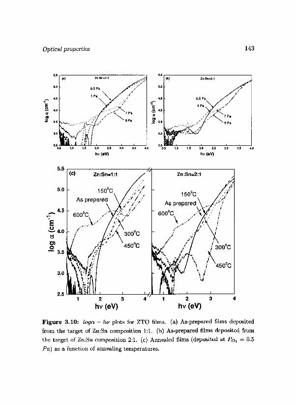
Optica.l properties
5.5 (0)
5 ••
•• S
'e g. ... " tII .2
Zn:Sn=1:1 ,.,:;;.;., ,
1 Pa /"
, ijO' ••••••• /
':>~'<::-7 Pa ,/ 9Pa
1.5 2,0 2.5 3.0 3.$ 4.0
hv (ey)
5.5 (b)
5'"
... ~ g. .... " co .E • .5
143
Zn:Sn=2:1
;;. ;
l' 0.5 Pa / ,. 1 Pa
" ,
,'<,z ,.' >~7pa
!" ;' .... ~ . .,. 9 Pa
1.D 1,5 2.0 2.5 :to 3.5 4.D
hv (eY)
5.5 r-------------I'A----------------.
5.0
4.5 .... rE ~4.0 ~
en o
- 3.5
3.0
(c) Zn:Sn=1:1 Zn:Sn=2:1
As prepared
600°C
\
2.5 LalILl!.IL:i.!..Lll---L-__ ---L-__ ...Lf'~....LJ.--li------'L---"----------.J
2 3 4 2 3 4
hv (eV) hv (eV)
Figure 3.10: loga - hv plots for ZTO films. (a) As-prepared films deposited
from the target of Zn:Sn composition 1:1. (b) As-prepared films deposited from
the target of Zn;Sn composition 2:1. (c) Annealed films (deposited at po. = 0.5
Pa) as a function of annealing temperatures.
144 Characterisation of ZTO Thin Films Prepared by PLD
tions observed in the films deposited at low P02 [Figure 3.1O(c)J, and 300
DC annealing increases the Tauc gaps to> 2.8 eV as shown in the inset to
figure 3.9c. The large increase in the subgap absorption for the 600 DC an
nealed films would be attributed to a strong reduction condition prevailing
at high temperatures leading to high oxygen deficiency.
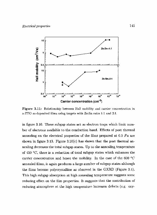
3.6 Electrical properties
Electrical properties of the as-deposited a-ZTO film~ are summarized in
figures 3.11-3.13. Previous works on a disordered crystalline oxide semi
conductor [180] and amorphous oxide semiconductors [126, 179, 181] indi
cate that carrier concentration should exceed a threshold value to obtain a
large mobility needed for semiconductor devices with active layers having
structural randomness. Similar to them, Hall mobilities comparable to or
greater than 10 cm2 IV s were obtained in the a-ZTO films when the carrier
concentrations exceeded 1016 cm-3 for the Zn:Sn = 2:1 films and 1018
cm-3 for the Zn:Sn = 1:1 films.
Figure 3.12 shows the controllability of the carrier concentration for as
deposited ZTO films. Carrier concentration can be controlled from 1012 to
1019 cm-3 by varying P02 from ° to 5 Pa. The large carrier concentrations
and mobilities are obtained for the films grown at P02 in the range of 2
- 7 Pa. The decrease of carrier concentration at higher P02 is due to the
suppression of the oxygen vacancies that may contribute to the formation
of donor states. However, the low carrier concentrations at low P02
are
not common in PLD deposited transparent conducting oxides. It could be
explained for the ZTO films by the large subgap states below 3 eV observed
Electrical properties 145
10
ii) ~ '" E
/-. / Zn:Sn=l:l
........... --........ --• u ->. :5 0.1
:c 0 10 E "ii I
.'
/ -..--~ Zn:Sn=2:1
Carrier concentration (cm"3)
Figure 3.11: Relationship between Hall mobility and carrier concentration in
a-ZTO as-deposited films using targets with Zn:Sn ratio 1:1 and 2:1.
in figure 3.10. These subgap states act as electron traps which limit num
ber of electrons available to the conduction band. Effects of post thermal
annealing on the electrical properties of the films prepared at 0.5 Pa are
shown in figure 3.13. Figure 3.1O(c) has shown that the post thermal an
nealing decreases the total subgap states. Up to the annealing temperature
of 450°C, there is a reduction of total subgap states which enhances the
carrier concentration and hence the mobility. In the case of the 600°C
annealed films, it again produces a large number of subgap states although
the films become polycrystalline as observed in the GXRD (Figure 3.4).
This high sub gap absorption at high annealing temperature suggests some
reducing effect on the film properties. It suggests that the contribution of
reducing atmosphere at the high temperature increases defects (e.g. oxy-

146 Characterisation of ZTO Thin Films Prepared by PLD
'1 10"
E ~.-~ . ~" >0- 10' ~ ~ ... 'jij yl ~S""~ c: ID
"C 10' ..
ID .;: ./ ... 1\1 0
10"
10' --E I.)
~ 10"
~ :~ 10~ () ::::I
"C 10" c:
0 0
o 2 4 6 8 10
Oxygen partial pressure (Pa)
Figure 3.12: Dependence of carrier transport properties of ZTO films on oxygen
partial pressure for the as-deposited films.
gen deficiencies) and localized states, which increases the film resistivity.
This leads to a reduction in carrier concentration and hence the mobility
(subsequently a higher resistivity) in the case of films annealed at 600 QC.
3.7 Conclusion
The structural, electrical and optical properties of amorphous zinc tin oxide
films deposited by pulsed laser deposition were investigated for two Zn/Sn
compositions as a function of oxygen partial pressure (P02) and annealing
temperature. The effects of post deposition annealing on the optical and
electrical properties of ZTO films were also examined. It was found that

Conclusion 147
e- 10' <>
9.. ~ 10'
~ '" 'u; 10' 11> a:
10·
iiI 6
~ E .!:!.
~ :c 0
::E
"l; 10" .!:!. .., I: • 0 rt ! l;. . c .. .. 10"
~ <> I: 0 <> a;
..... In:Sn=2:1 'E • .. -.- Zn:Sn=l:l 0 10"
0 100 200 300 400 SOO 600
Annealing temperature (oC)
Figure 3.13: Dependence of carrier transport properties of ZTO films on post
annealing temperature for the films deposited at po. = 0,5 Pa,

148
optical absorption spectra showed strong subgap absorptions for the films
deposited at P02 < 2 Pa. Tauc gaps of the ZTO films were increased
to 2.85 eV on deposition at high P02 or post thermal annealing, which
resulted from the reduction of the subgap states. The carrier concentration
- P02 relations showed broad peaks, which is explained by the existence
of the electron traps in the sllbgap states for the films grown at low P02
and by the reduction of the oxygen vacancies on deposition of films at high
Po2 • The high electron concentration films were shown large Hall mobilities
greater than 10 crn2 IV s.