Embed Size (px)
Citation preview

University of North Carolina at Chapel Hill Department of Computer Science
CHARACTERIZATION AND ANALYSIS OF
PROGRAMMABLE SWITCH DESIGNS
Margaret F. Loaplnuao April 11185
Technical Report TR85-005

CHARACTERIZATION AND ANALYSIS OF
PROGRAMMABLE SWITCH DESIGNS
Margaret F. Lospinuso The University of North Carolina at Chapel Hill
April 1985
Abotract
The object of the experiments described here was to guide the design effort by characterizing the signal transmission time and power consumption of switch designs proposed for the WAfer-scale Systolic Processor (WASP) project. Three design layouts and one fabricated design were tested. The experiments showed that by revising the design we could achieve a 50% reduction in signal transmission time while also reducing power consumption by 50%. The reduction was achieved by moving from a three-inverter superbufrcr design to a two-inverter switch using precharge. The experimental results strongly reinforce the observation that design must be guided by analysis, and that careful use of simulators can bring significant improvements before fabrication. The result of these experiments was a switch that is practical for use in a wafer-scale processor, and, therefore, the knowledge that we can build a wafer-scale processor.
Contents:
I. Objective 2. Experiments
2.1 Theoretical Model 2.2 Simulation
2.2.1 The Simulation Programs 2.2.2 The Testbed 2.2.3 Circuits Tested 2.2.4 Definition of Signal Transmission Time 2.2.5 Test Input 2.2.6 Results
2.2.6.1 Delay 2.2.6.2 Power Consumption
2.3 Test Structures Chip 2.3.1 Layout 2.3.2 Tests Conducted 2.3.3 Test Results
3. Conclusion

1. Objective
For certain special purpose computations systolic architectures have the potential for very high perrormance. A wafer-scale implementation, in which processing elements are connected by a mesh of programmable switches on a single wafer, offers the best means for optimizing speed and reliability in systolic arrays. The smaller size and lower capacitance of on-chip wiring permit higher speed than can be obtained with discrete chips and external wiring. On-chip interconnection also brings greater reliability through a reduction in the number of components, and the programmable switch matrix lessens the impact of faults by permitting the inclusion of red undant processors and the local exclusion or bad processors.
The W Arer-scale Systolic Processor (WASP) project is focussing on both the logical problems of wafer-scale integration, such as system decomposition, component redundancy and wire routing, and the physical problems, such as power consumption, defect frequencies and design of components suitable for the mesh of programmable switches ]Hedlund84]. The programmable switches are a key aspect of both the logical and physical aspects of the design, since the WASP approach to systolic processor design requires that the switches route data around bad processing elements and implement the data paths needed for the execution of systolic algorithms. The objective of this study has been to characterize proposed switch designs.
The intent of the characterization is to derive detailed performance information on programmable switch designs for the WASP project, information to be used as a baseline in judging the performance of new switch designs. Because of the requirements of the WASP design, switches must be optimized for speed, power consumption, area and complexity, tradeoffs that usually conflict.
WASP switches must not only provide the capability to route data and exclude bad processing elements from the mesh of processing elements, they must also be transparent to the logical design. Algorithms are mapped onto the mesh of processing elements as if there were nothing but short programmable wires between processing elements. A signal must be able to propagate from the output of a processing element through one to twelve switches in a single clock cycle, so that the output of a processing element is received by its logical neighbor in the same cycle. This propagation length requires that switch designs be optimized for speed. However, since power consumption is an important limiting factor in wafer-scale design, the required speed must be gained at a minimum expenditure of power.
Along with speed and power constraints are size constraints. Switches must be small and simple so that there are few components that can fail, and so that adding redundant switches costs only a modest amount of silicon.
The goal of the new designs, then, is to improve speed and reduce power consumption, while minimizing size and complexity. Detailed characterization is being used to guide the design effort.
z. Experiments
The characterization comprised three phases: construction of a theoretical model, simulation of layouts, and 'fabrication and testing of a switch design. Both the simulation testbed and the fabricated chip were designed to place the switch into an environment that was as close as possible to its intended working environment but that would allow close observation of the switch.
:!.1. Theoretical Model
The theoretical model serves to derive estimates that will be used as a rough check of the more precise results that can be expected from SPICE. Theoretical discussions of delay appropriate to the switch circuit and its transmission line have been published by Penfield and Rubinstein ]Penfield81] and Rubinstein, Penfield and Horowitz ]Rubinstein83], who discuss delay in RC trees, by Ousterhout ]Ousterhout84], who develops both RC and slope based models, by Antinone

[Antinone83J, who gives results on the use of a ladder of L-networks, and by Sakurai [Sakurai83J, who simplifies the work of Penfield and Rubinstein, compares the use of an analytical model and lumped circuit approximations, and establishes the appropriate types of lumped circuit approximations as a function of the ratio of the drive resistance to the wire resistance and the wire capacitance to the load capacitance.
Penfield and Rubinstein focus on uniform RC trees, that is, circuits with fanout> 1, and do not include pass transistors in their RC lines. The WASP switch has the capability for a fanout of four, but it is being used with a fanout or one in this test sequence because we anticipate that, although the switch must be able to direct the signal in multiple directions, most systolic algorithms require that the signal be propagated on a single path in a given cycle. Furthermore, the directional switching is accomplished with pass transistors, which are not included in the Penfield and Rubinstein model.
Ousterhout uses the Penfield-Rubinstein model and a division or the circuit into stages comprised generally of one transistor to arrive at a delay model whose delay is expressed as the sum of the stage delays.
Antinone's principal focus is on the transmission properties of long resistive interconnects. His results show that lumped element RC ladder networks can be used to get a good approximation of delay time using relatively few sections. His basic element is a L-network, consisting or a single resistor and capacitor; these L-networks are linked into a ladder network. A two-section ladder gives results that are close to that predicted by transmission line theory; a five section ladder gives yet closer correspondence to the theoretical results, but there is little difference betweeen the results obtained from a five-section ladder and a 10-section ladder. This suggests that for approximating the WASP switch delay there should be greater than two L-networks in the ladder, but not more than five.
Sakurai divides lumped circuit models into several types of models, from simple to more complex RC ladders, and analyzes the degree of error anticipated with each model in terms of the relation of the load capacitance to the wire capacitance and the driver resistance to the wire resistance. His basic model contains a single inverter driving an interconnect line and the gate of the next inverter. The WASP switch is somewhat more complex than this basic model since it has the pass transistors superimposed on the interconnect line. Antinone's work suggests that the pass transistors can be added to Sakurai's basic model in the form of additional L-networks. From the ratio of the drive resistance to the wire resistance (including the pass transistors as wire resistance), and the ratio of the load capacitance to the wiring capacitance, if an error of 3% is admitted, Sakurai's results recommend the use of a pi-network to model the interconnect line, as shown in Figure 2.1.1a. Adding the pass transistors modifies the basic model as shown in Fig· ure 2.1.1b. Converting these pass transistors and the drive transistor and its source capacitance into L-networks produces the ladder of L-networks shown in Figure 2.1.1c. This series of Lnetworks can be solved by modeling each L-network as a switched circuit, where the switch of all the L-networks is closed at t=O, and the voltage across the capacitor of each L-network is the input voltage seen by the subsequent L-network. Figure 2.1.2a shows the basic switched-circuit model of the L-network, and Figure 2.1.2b shows the RC ladder modelled with switched circuits. Note that the circuit is being modelled for the zero to one transition, which is longer than the one to zero transition for nMOS circuits; the model thereby adopts the worst case as its basis.
There are several important simplifications involved here. A linear resistor is being used to approximate the depletion mode driver; this is generally considered an acceptable simplification for approximating devices [Hodges83[. The drain/source capacitances of all devices are modelled as simple capacitors. By extension of the modeling or the load device, the pass transistors are also modelled as resistors. This is the weakest aspect of the modeling, since a pass transistor is not a linear device, and will cause a threshold drop in the voltage, an aspect that is not modelled by the substitution of resistors. For this reason, these calculation results are not accurate above Vdd-Vth. As Hodges and Jackson point out, accurate mathematical modeling involves higher
3

order polynomials, work they feel is best Jert to SPICE. The model, then, serves as an approximate check on the SPICE results.
Each L-network switched circuit solves easily as a first order partial differential equation, as follows:
From Kirchoff's voltage Jaw
Substituting for i we get
which has a solution of the form
Vo.+1(t)- VoP•+1(t)+Be''.
Since when we replace the output voltage with a constant the derivative in equation 2 is zero,
VoP•+l( t)= Vo,.
And the output at t(O+) is zero, so
Then we have
B=-Vo •.
.=L Vo.+1(t)= Vo.- Vo. e RC.
(1)
(2)
(3)
(4)
(6)
(8)
Repeatedly solving this equation, using the result from one L-network iteration as the input voltage for the next L-network iteration, we see that the transmission time should be about 10 nanoseconds. This iteration effectively divides the circuit into stages, and produces a solution in a manner similar to that used by Ousterhout. Figure 2.1.3 shows the output voltage from the last L-network in the ladder. These results are in close agreement with the results predicted by SPICE (see section 2.2.6) and the transmission time measured on the test structures chip (see section 2.3.3). They are heavily dependent upon the accuracy of the estimation of resistance and capacitance, both of which may vary significantly from fabrication to fabrication, and they treat transistors as purely linear devices, which they are not. It is more burdensome to derive the model equation and perform the calculations than it is to invoke SPICE with the input file preparation tools at hand; nevertheless the model provides a fairly accurate check on the validity of the SPICE output. Futhermore, many results may be understood from the equation through simple contemplation or its implications.
:t.:z. Simulation
The simulation of layouts required that appropriate simulation programs be chosen and that a suitable testbed be constructed, a testbed that would allow different switch designs to be placed into a constant environment. SPICE makes assumptions about the initial conditions of the circuit; it proved better to provide a testbed that isolated the recorded result from these assumptions than to force SPICE to abandon its view of the initial conditions. The testbed had to provide a framework into which various switch designs could be inserted, a framework that would model a wafer-scale processing section under the size restrictions imposed by SPICE. Both the simulation programs and the testbed are discussed further below.

A.
B.
R1 c.
R1 -l
C1
R1
-l r""T""vvv-,----1~ C4
C2 C3
C2 C3
R2 R3 R4
C2 C3 C4
Figure 2.1.1 Steps in Modeling the WASP 1.3 Switch
5

R
t=~ c
R1 R2 R3 R4
.--"' ----"w.,.., ----,l.--c-;-v.""'~'r·1-l,_c-2_+_v .... ~.,.., 2---,1.--c-~-v.""':-I
=Ydd
Figure 2.1.2 Switched Circuit Model of the WASP 1.3 Switch

v
3
2
1
0
0 5 10 15 ns
Figure 2.1.3: Output or the Final L-network in the RC Ladder
7

2.2.1. The Simulation Program•
Two simulation programs were used, SPICE [VIadimirescu81[ for electrical simulation and POWEST [Cmelik81) for estimating power consumption.
Several separate SPICE simulations were conducted, each with different parameters. The SPICE simulation parameters used for these simulations were those supplied by MOSIS in June 1984 for the upper limit fabrication, the nominal fabrication and the lower limit fabrication, and those supplied by MOSIS for its November 1984 run M4ABVL1, the run on which the switch test structures chip described in section 2.3 was fabricated. On these runs lambda was equal to two microns; the minimum device size was four microns.
There are severe size constraints on circuits that can reasonably be modelled with SPICE; these size constraints run counter to the need to include not only the switch but also an accurate model of its operating environment. The test environment, then, had to resemble the actual environment closely in its electrical characteristics, but it had to be restricted in scope so that it would be small enough for accurate simulation to be feasible. For this purpose a medium-size simulation testbed was constructed.
In order to achieve as much accuracy as possible, the power simulator, POWEST, was recompiled using parameters from MOSIS run M4ABVL1. Power estimates were derived for a single switch or each type.
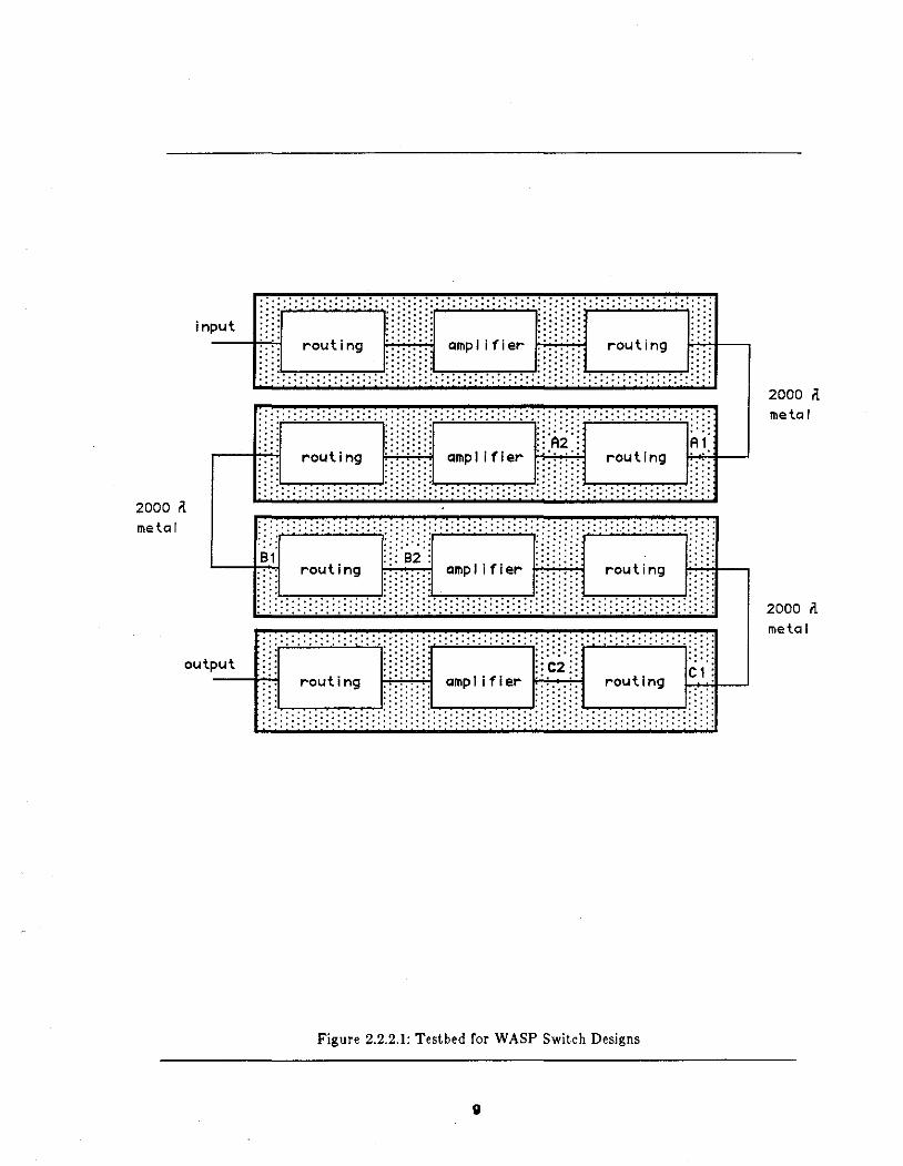
2.2.2. The Testbed
The testbed constructed for the simulation comprised four switch modules interconnected by 2000 lambda of metal wire. This separation between switches is intended to model that expected in a full-size systolic processor. The distance between switches in the mesh is determined by the size of the processing elements embedded in the mesh. The processing elements in WASP 1.1--1.3 are minimal processors, about 350 x 350 lambda, and switches are separated by this distance. The more powerful processing elements of a production systolic processor will be not more than 2000 lambda on a side, which dimension gives an upper bound on the distance between switches.
The switch module routing sections each consisted of a single pass transistor with its gate tied to VDD, but with the same diffusion drain/source area as would be required for the fourway switch used in WASP 1.1--1.3. The removal of these six unused pass transistors from the input file greatly simplified the use of SPICE but was transparent in the result. (See section 2.2.3 for a more detailed description of the circuits tested.) The first switch served to isolate the test apparatus from the input signal, so that the second and subsequent switches would see the waveform that the switch is capable of generating instead of a test input square wave. Values were recorded at the six points A1,A2, ... C2 labelled in Fig. 2.2.2.1. Three pairs of test points were chosen to reduce the possibility of error in transcribing the results from the SPICE output files (since the pairs had to correspond closely to be correct) and to reduce the effects of local variance by increasing the number of points of observation.
2.2.3. Circuits Tested
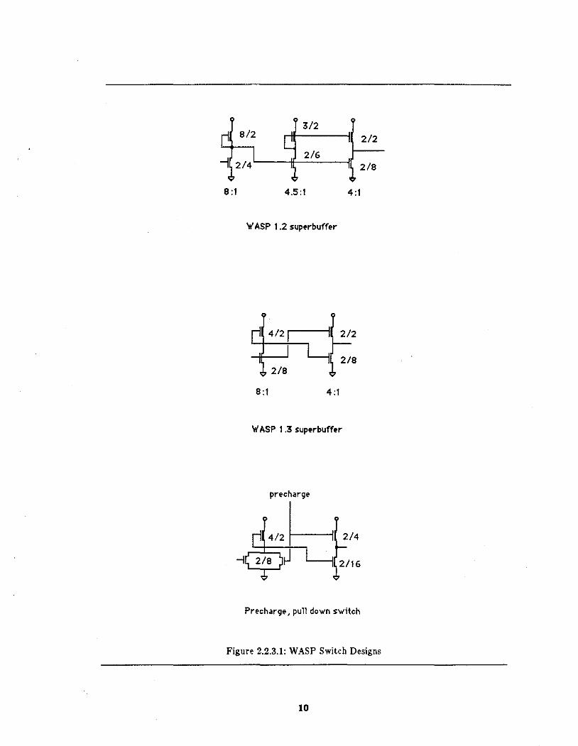
The three WASP switches (Fig. 2.2.3.1) that have been studied are of basically similar design. They pass a single signal, receiving it from any of four directions (N,S,E or W), and passing it to any single direction or combination of four directions, NSEW. The switches use a single amplifier to restore signals coming from all directions, and going to all directions; unwanted paths are isolated by pass transistors. There are three sections to the general switch design: input selection pass transistors for four directions (NSEW), the amplifier, and output selection pass transistors (also for NSEW). Routing pass transistor sizes were the same for all designs. The designs differ sharply in the amplifying section, both in the number and the sizes of transistors used. The number of inverters was reduced to achieve lower power consumption; the transistor sizes in the inverters were optimized individually for each design.
8
2000 il meta I
input
output
. . . . . . . . . . . . . . . . . . ·.·.·.·.·.·.·.·.·
routing
. . . . . . . . . . . . . . . . . . . . . . . ·.·.·.·.·.·.·.·.·
routing
·:·:-::;:;:;:;:;:;:;::
........... . . . . . . . . . . . .. ·.·.·.·.·.·.·.·.·
81 routing
. . . . . . . . . . . . . . . . . . . . . . . . . . . . . . . . . . . . . . . . . . . . . . . . . . . . . . . . . . . . . . . . . . . . . . . . •,•,•,•,•,·,·.·.·
routing
. . . . . . . . . . . . . . . . . . . . . . . . . . . . . . . . . . ' ....... . . . . . . . . . .
. ....... . ......... . . . . . . . . . .........
amp I i fier
. ....... .
amp I i fier
......... ............ . . . . . . . . . . . . . . . . . . . . . . . . . . . . . . . . .
82
. . . . . . . . . . . . . . . . .
amp I i fier
. . . . . . . . . . . . . . . . . ......... . . . . . . . . . . . . . . . . . . . ....... . . . . . . . . . . . . . . . . . . .
amp I i fier
........ . . . . . . . . . . ....... . . ....... . . . . . . . . . . . ....... .
C2
.......... . . . . . . . . . ·.·.·.·.·.·.·.·.·.·
routing
::: ::::::::::::::: :-:.:
............ . ......... . ·.·.·.·.·.·.·.·.·.· .. A1
routing
;:;:;:;:;:;:;:;:;:;.:-:
. ......... . ............ . ·.·.·.·.·.·.·.· ..
routing
....... . ......... . . .......... . . . . . . . . . . . . . . . . . . . . . . . . . ......... . . ......... . . .......... . . ......... . .......
routing C1
. ..... . . ....... . . ........ . . ....... . . ........ . . ....... .
Figure 2.2.2.1: Testbed for WASP Switch Designs
II
2000 il metal
2000 il metal
3/2 r 8/2 ~ 2/2
I 2/6 --f 2/4 " 2/8
o!> ~ o!>
8:1 4.5:1 4:1
WASP 1 .2 superbuffer
8:1 4:1
WASP 1 .3 superbuffer
Precharge, pull down switch
Figure 2.2.3.1: WASP Switch Designs
10

Three switch designs circuits were tested, The WASP 1.2 switch, the WASP 1.3 switch, and a third as yet unfabricated design. The WASP 1.2 switch uses a three-inverter super buffer for level-restoring and driving. The second switch tested uses a two-inverter super buffer. This switch was fabricated on the test structures chip and in WASP 1.3. The third circuit tested was a new design, using a precharging scheme for level-restoring, with a single inverter to pull down the precharged line. The three circuits represent a progression, from a lear cell derived from a standard cell whose function was known to be correct, to a refinement of the first attempt, and then consideration of an entirely new scheme. The WASPI.2 switch was known to be powerhungry and slow, but it did function, and could be used in a first design. The WASP1.3 switch was a refinement of this design--once the first design could be shown to work, it was time to improve it. The third design, the precharge scheme, came from a total change in concept. We had squeezed the maximum performance from the second design but found it only adequate. Better speed and lower power consumption were still wanted, which meant that it was time to step back and take a fresh look.
:Z.:Z.4. Definition of Signal Transmission Time
The transmission time for one switch to send a signal to the next switch was determined to be the time elapsed between the point at which the input gate of the first switch reached the logic inversion voltage, Vinv, and the input gate of the next switch reached Vinv. During this time the signal passes through the switch inverters, the switch output routing section, and the 2000 lambda of metal wire separating the switches, and the input routing section of the second switch. Mathematically,
Transmission time= T(Bl=Vinv)- T(Al=Vinv) = T(Cl=Vinv)- T(Bl=Vinv) - T(B2=Vinv)- T(A2=Vinv) = T( C2= Vinv) - T(B2= Vinv)
This measurement of transmission time differs slightly from that used by Hodges and Jackson [Hodges83J, but seems closer to the intent of their definition. They define propagation time as the
delay between the 50% points on the waveforms'. In general it is desirable that the voltage margins around the logic inversion point be approximately equal [Mead80]; however, simulation results showed that the logic inversion point would be slightly lower than 50%, meaning that the switches would turn on sooner but would be slower to turn off. Since a switch that has reached the logic inversion point can be considered to have "heard" the signal, the inversion point was selected in preference to the 50% point. The actual difference on the delay estimation using the 50% point and the logic inversion point was minimal, but extraction or the logic inversion point from the SPICE files was simpler than calculating the 50% point. The logic inversion voltage, Vinv, was determined by using SPICE to get the de transfer curve for the switch inverters, and measuring Vinv as the point at which the input and output voltages of the inverter were equal.
Delay is sometimes measured as the time required for the voltage at a given point to swing from 10% to 90% peak-to-peak. It is a convenient measurement since it requires knowledge of only a single point, and thus does not require point-to-point comparison. However, the experience derived from the experiments here is that the peak-to-peak time is related to power consumption in the circuits that did not use precharge and to gate width in the precharged circuits. It is not related to the point-to-point rise to the logic inversion voltage described above. The 10% to 90% peak-to-peak value is in effect an overly conservative measure, since it does not describe the time it takes a node to be transmitting a new value. The rise from 50% to 90% consumes more time in low-power circuits than in higher-power circuits. This is obvious from the higher slope in the rise time curve on higher-power circuits. The upper part of the curve tends to level out in lower-power circuits, as if the last volt were harder to dr!ve. Since it is the 10% to
1There seem!! to be no common &gTeement on the definition of propagation time. [Ohkura.83] ddinee: propa..gation time u the delay between the times the input and output wavefortiUI reach the three:hold volta.ge; thie: definition e:eems likely to
11

logic inversion voltage time segment that actually determines how long it takes to transmit the signal, and this time segment is not as sharply affected by power consumption in the switch designs used in WASP implementations, the 10% to 90% time does not adequately describe delay in this circuit.
t.Z.5. Test Input
The input signal consisted of a 120 ns square wave, with a rise and fall time of Ins and a pulse width of 58ns. In each simulation a transient analysis was run for 240 ns, and timings were read for the rising transition on the second pulse (falling transition on the precharge design). Using the second pulse had the effect or isolating the experiment from the assumptions SPICE makes about the initial conditions or nMOS inverters.
t.t.!l. Results
The experiment showed that we could simultaneously increase speed and reduce power con, sumption by moving to a different type or switch design, one using a precharge scheme.
:t.z.!l.l. Delay
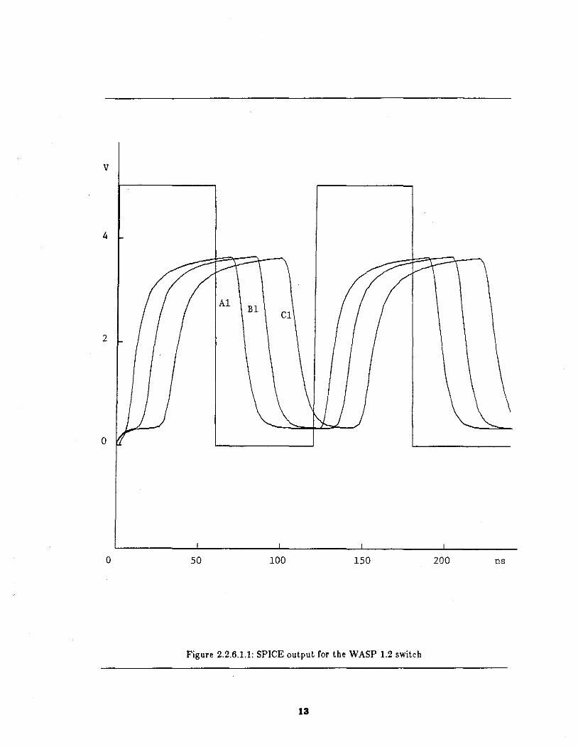
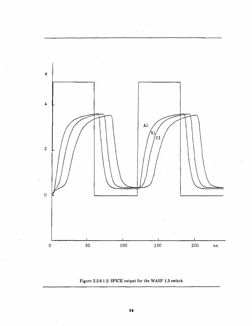
The average delay at the three points reeorded in the SPICE simulations is recorded in Table 1. The delay times show that the WASP 1.2 switch had an unacceptable performance using the parameters from the lower limit fabrication; no output pulse was detectable using an input pulse of 58ns. The output wave forms for each or the three pairs of recorded points in the WASP1.2 switch show that the pulse became progressively wider as it passed through successive switches in the chain. This widening effectively limits the number or switches through which a signal may be expected to pass in a single clock cycle at a given speed. Figure 2.2.6.1.1 shows the SPICE output wave forms for the WASP 1.2 switch; Figure 2.2.6.1.2 shows the SPICE output wave forms for the WASP 1.3 switch, showing obvious improvment over the WASP 1.2 switch.
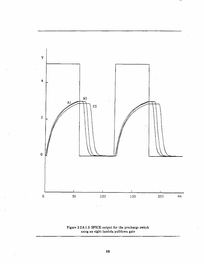
Two sets of results are shown in Table 1 for the proposed circuit using a precharge scheme. The first series of experiments showed an surprising degree or sensitivity to the width or the gate pulling down the pre charged wire between switches. Analysis or the RC values showed that some sensitivity should be expected and that we should expect to get significantly better pull-down time with a wider gate, but the degree or sensitivity observed in the SPICE output also provoked careful field-by-field study or the automatically generated SPICE input file.
In order to enforce uniformity or result a circuit extractor-to-SPICE-input conversion tool, CIF2SPICE [Bishop83J, was routinely used. Detailed study or the SPICE input files 1•·ovided by CIF2SPICE showed that it had yielded an unnecessarily conservative estimation of the RC values, and the SPICE input files were accordingly revised by hand. These revised files were then run with SPICE using only the nominal and upper limit fabrication parameters, since by this time MOSIS, through a program of screening results from vendors, had achieved a minimal fabrication quality well above the former minimal level. The r•"ision netted some improvement in signal transmission time. Overall, a 50% reduction in signal transmission time ret ween the WASP 1.2 switch and the proposed precharge design was gained. Figure 2.2.6.1.3 shows the output wave forms of the revised SPICE files using an eight lambda wide gate, and Figure 2.2.6.1.4 shows the same simulation using a two lambda wide gate, with the resulting slower transmission
introduce confu:~ion between thre!lhold voltage of a tra.uistor aud logic inven:ion voltage of an inverter.
v
4
2
0
0 50 100 150 200 ns
Figure 2.2.6.1.1: SPICE output for the WASP 1.2 switch
13
v
4
2
0
0 50 100 150 200 ns
Figure 2.2.6.1.2: SPICE output for the WASP 1.3 switch
v
4
2
0
0
B1
C1
50 100 150
Figure 2.2.6.1.3: SPICE output for the precharge switch using an eight lambda pulldown gate
15
200 ns

v
4
2
0
0
B1
C1
50 100 150
Figure 2.2.6.1.4: SPICE output for the precharge switch using a two lambda pull down gate
111
zoo ns
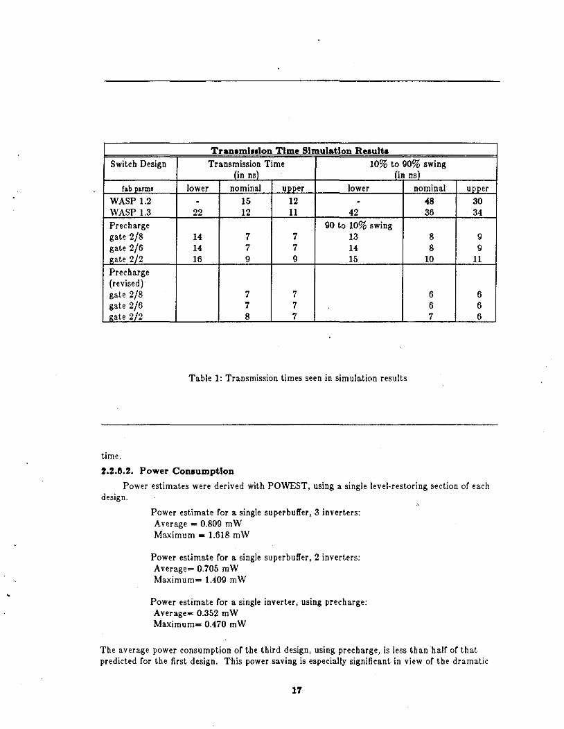
Tranomloolon Time Simulation Reoulto Switch Design Transmission Time 10% to 90% swing
(in ns) (in ns)
lab P&nns lower nominal upper lower nominal upper
WASP 1.2 - 15 12 - 48 30 WASP 1.3 22 12 11 42 36 34 Precharge 90 to 10% swing gate 2/8 14 7 7 13 8 g
gate 2/6 14 7 7 14 8 g
gate 2/2 16 9 9 15 10 11
Precharge (revised) gate 2/8 7 7 6 6 gate 2/6 7 7 6 6 gate 2/2 8 7 7 6
Table 1: Transmission times seen in simulation results
time.
%.2.11.2. Power Conoumptlon
Power estimates were derived with POWEST, using a single level-restoring section of each design.
Power estimate for a single super buffer, 3 inverters: Average= 0.809 mW Maximum= 1.618 mW
Power estimate for a single superbuf!er, 2 inverters: Average= 0.705 mW Maximum= 1.409 mW
Power estimate for a single inverter, using precharge: Average- 0.352 mW Maximum= 0.470 mW
The average power consumption of the third design, using precharge, is less than half of that predicted for the first design. This power saving is especially significant in view of the dramatic
17

decrease in signal transmission time and the reduction in size associated with this design.
%.3. Test Structure• Chip
The test structures chip was designed to allow measurement of switching speed in such a manner that the switch would be operating in an environment close to what is expected in a systolic array, but could be studied from the exterior of the chip with the effects of the instrumentation transparent in the result. It consists of two mirror-image halves, each of which contains three different types of chains of switches.
J.3.1. Layout
Switch chain no. 1 (see Fig. 2.3.1.1) comprises a metal input pad (with lightning arrester but no driver circuitry) and a chain of 15 switches. Between each switch is 1180 lambda or metal, 45 lambda of polysilicon, and an output pad with superbuffer. The total load is intended to be somewhat greater than that seen by a switch driving 2000 lambda of metal, and the interspersed output pads afford the opportunity to watch single switches and groups of switches to observe signal transmission times.
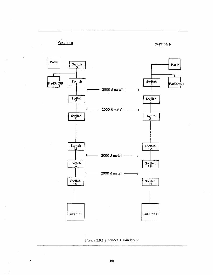
Switch chain no. 2 is present in two versions (see Fig. 2.3.1.2). Version a has an input pad (with driver circuitry) that drives a single switch (switch 0). This switch then drives both an output pad (with pad driver) and a chain of fourteen switches. The fourteenth switch drives an identical output pad. Version b has much the same structure except that the input pad drives both the chain of fourteen switches and and output pad. The fourteenth switch again drives an output pad. A 2000 lambda metal wire goes between each switch.
The switch design is the two-inverter super buffer design also used in WASP 1.3 (see Fig. 2.3.1.3). In the routing sections the three pass transistors that are not needed for signal transmission (the signal is being passed from west to east only; the north, ·south, west-out and east-in routing pass transistors are unneeded) are tied to ground. The gate voltage supply for the routing pass transistors that are intended to transmit the signal is tied in all three chains to a separate power supply line (PadVHot), so that the effects of gate voltages higher than 5V could be studied.
2.3.:1. Teato Conducted
Each chip was mounted on a test stand with connections to power supply and ground. The input signal was provided by a signal generator, and the output was observed on an oscilloscope. Signal transmission times were recorded at two output pads, one receiving its signal directly from an input pad, the other receiving its signal from a chain or switches driven by the same input pad. The transmission time was defined as the difference between the time the signal passed through the 50% points on the two output pads. To provide feedback on the accuracy of the SPICE simulations, one further SPICE run was done, using the actual fabrication parameters with the fabricated design on the simulation testbed.
2.3.3. Teot Resulto
The average delay using a gate voltage or 5V was 9.9ns per switch. Using "hot clocking." with the gate voltage at 8V, the delay was reduced to 8.4 ns per switch. There was variation observed in the times recorded for the same chain in different positions on the same chip and for the same chain on different chips (7 chips were fabricated). The shortest delay recorded was 8.7 ns; the longest was 10.4ns. The switch chains could be operated comfortably up to 5Mhz. Operation was still possible up to lOMhz, but although there was still a clear output pulse, there was no longer a 50% duty cycle output for a 50% duty cycle input. Figure 2.3.3.1 shows the output of one sample of switch chain no. 2, version b. The delay between the rise times is 143ns for a chain or 14 switches, or about 10.2ns per switch.
The SPICE runs utilizing the MOSJS fabrication parameters from the run on which the test structures chip was fabricated yielded an average signal transmission time of 9ns per switch.
18

70 ,t poly I . l PadlnBlnk I sw1tch 1
1180 4 metal ---+
45 ,t poly i PadOutSB 1
I switch 2 I
PadOutSB 2
I I switch 141
PadOutSB 14
I switch 15 1
PadOutSB 15
Figure 2.3.1.1: Switch Chain No. 1
111
Version e Version b
Padln Padln
PadOutSB I
1 swreh 1 PadOut~ B
2000 II meta 1
I Swdteh I 2000 II meta 1
f Swleh l I ,. ' l
2000 II meta 1
2000 II metal
PadOutSB PadOutSB
Figure 2.3.1.2: Switch Chain No. 2
20

I Gnd output VHot
Figure 2.3.1.3: Switch Element
tl

v
5
3
1
3
1
0 40 80 120 ns
Figure 2.3.3.1: Switch Chain Output

This is within one nanosecond of the result obtained from testing of the fabricated circuits and is well within an acceptable degree of accuracy.
3. Conclualono
The experimental results strongly reinforce the observation that design must be guided by analysis, and that careful use of simulators can bring significant improvements before fabrication is attempted. The experiments showed that by using a precharge scheme we could expect a 50% reduction in signal transmission time while also reducing the expected power consumption by more than 50%. Furthermore, the precharge design is simpler and smaller than the WASP 1.2 switch that was the first design tested. A by-product of the experiments was confirmation that our circuit simulator is indeed reasonably reliable, that results from fabrication can be expected to agree closely with simulation results for circuits similar to those used in WASP switch designs.
The experiment began with a power-hungry superbuffer, included testing of three designs in simulation, using a specially constructed simulation testbed, and testing of fabricated integrated circuit chips using one of these designs in a special fabrication test structure. It concluded with the decision to make a fundamental change in design strategy with the adoption of a precharge scheme. The experiments resulted in a switch that even in four micron nMOS is fast enough for a practical wafer-scale design; this, of course, implies that as we move to smaller dimensions in nMOS and to CMOS, we can achieve even better performance and lower power consumption, and we know that we can build a wafer-scale processor.

REFERENCES
[Antinone83[. Antinone, Robert J. and Gerald W. Brown, "The Modeling or Resistive Interconnects for Integrated Circuits." IEEE Journal of Solid-Stale Circuita, SC-18 (April 1983), 20().203.
[Bishop83[. Bishop, Gary. Cif!Japice, UNC-CH CAD Tools, 1983.
[Cmelik81j. Poweat, Berkeley CAD Tools, 1981.
[Hedlund84). Hedlund, Kye S, and Lawrence Snyder, "Systolic Architectures- A Water Scale Approach" Proceedinga of the IEEE ICCD 1984, pp. 604-609.
[Hodges83J. Hodges, David A. and Horace G. Jackson. Anal11m and Delign of Digital Integrated Circuita. New York: McGraw-Hill, 1983.
[Mead80). Mead, Carver and Lynn Conway. Introduction to VLSI Systema. Reading, MA: Addison-Wesley, 1980.
[Ohkura83). Ohkura, !sao, Kaoru Okazaki, Takeshi Tokuda and Kazuhiro Sakashita. "VLSI Design Verification and Logic Simulation." In: Hardware and Software Concepts in VLSI, ed. by Guy Rabbat. New York: Van Nostrand Reinhold, 1983.
[Ousterhout84). Ouster bout, John K. "Switch-Level Delay Models for Digital MOS VLSJ." In: ACM IEEE !Jlst Design Automation Conference Proceedings, 1984, pp. 542-548.
[Penfield81). Penfield, Paul Jr. and Jorge Rubinstein. "Signal Delay in RC Tree Networks." In: IEEE 18th Design Automation Conference Proceedings, 1981, pp. 613-617.
[Rubinstein83J. Rubinstein, Jorge, Paul Penfield, Jr., and Mark A. Horowitz. "Signal Delay in RC Tree Networks." IEEE Transactions on Computer-Aided Design CAD-2 (July 1983) 202-211).
[Sakurai83). Sakurai, Takayasu. "Approximation of Wiring Delay in MOSFET LSI." IEEE Journal of Solid-State Circuits SC-18 (August 1983) 418-426.