Embed Size (px)
Citation preview
Characterization and design of architectures for
phase-change memories based on alternative-to-GST
materials
Athanasios Kiouseloglou
To cite this version:
Athanasios Kiouseloglou. Characterization and design of architectures for phase-change mem-ories based on alternative-to-GST materials. Micro and nanotechnologies/Microelectronics.Universite Grenoble Alpes, 2015. English. <NNT : 2015GREAT128>. <tel-01278433>
HAL Id: tel-01278433
https://tel.archives-ouvertes.fr/tel-01278433
Submitted on 24 Feb 2016
HAL is a multi-disciplinary open accessarchive for the deposit and dissemination of sci-entific research documents, whether they are pub-lished or not. The documents may come fromteaching and research institutions in France orabroad, or from public or private research centers.
L’archive ouverte pluridisciplinaire HAL, estdestinee au depot et a la diffusion de documentsscientifiques de niveau recherche, publies ou non,emanant des etablissements d’enseignement et derecherche francais ou etrangers, des laboratoirespublics ou prives.
THÈSE
Pour obtenir le grade de
DOCTEUR DE L’UNIVERSITÉ GRENOBLE ALPES
préparée dans le cadre d’une cotutelle entre l’Université Grenoble Alpes et l’Université de Pavia
Spécialité : Nano Électronique et Nano Technologies et Microélectronique
Arrêté ministériel : le 6 janvier 2005 - 7 août 2006
Présentée par
Athanasios KIOUSELOGLOU Thèse dirigée par Fabien CLERMIDY et codirigée par Guido TORELLI préparée au sein du CEA-LETI dans l’École Doctorale Électronique, Electrotechnique, Automatique et Traitement du Signal (UGA) et au sein du Laboratoire des Microsystèmes Intégreés du Dipartimento di Ingegneria Industriale e dell’Informazione dans l’École Doctorale de Sciences de l’Ingenierie (UniPV)
Caractérisation et conception d’architectures basées sur des
mémoires à changement de phase Thèse soutenue publiquement le 17 décembre 2015 devant le jury composé de :
Monsieur Jean-Michel PORTAL Prof., Université d'Aix-Marseille (France) Président rapporteur
Monsieur Alessandro SPINELLI Prof., Politecnico di Milano (Italie) Rapporteur
Monsieur Alessandro CABRINI Ing., Université de Pavia (Italie) Encadrant
Monsieur Fabien CLERMIDY HDR, CEA-LETI, Grenoble (France) Directeur de thèse
Monsieur Luca PERNIOLA Ing., CEA-LETI, Grenoble (France) Encadrant
Monsieur Guido TORELLI Prof., Université de Pavia (Italie) Co-Directeur de thèse
Monsieur Jean-Michel MIRABEL
Ing., STMicroelectronics, Rousset (France) Invité

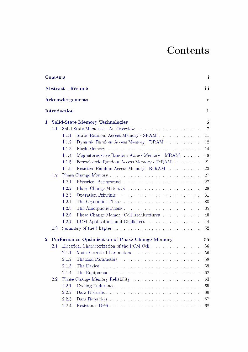
Contents
Contents i
Abstract - Résumé iii
Acknowledgements v
Introduction 1
1 Solid-State Memory Technologies 5
1.1 Solid-State Memories - An Overview . . . . . . . . . . . . . . . . . . 7
1.1.1 Static Random Access Memory - SRAM . . . . . . . . . . . . 11
1.1.2 Dynamic Random Access Memory - DRAM . . . . . . . . . . 12
1.1.3 Flash Memory . . . . . . . . . . . . . . . . . . . . . . . . . . 14
1.1.4 Magnetoresistive Random Access Memory - MRAM . . . . . 19
1.1.5 Ferroelectric Random Access Memory - FeRAM . . . . . . . . 21
1.1.6 Resistive Random Access Memory - ReRAM . . . . . . . . . 23
1.2 Phase Change Memory . . . . . . . . . . . . . . . . . . . . . . . . . . 27
1.2.1 Historical Background . . . . . . . . . . . . . . . . . . . . . . 27
1.2.2 Phase Change Materials . . . . . . . . . . . . . . . . . . . . . 28
1.2.3 Operation Principle . . . . . . . . . . . . . . . . . . . . . . . 31
1.2.4 The Crystalline Phase . . . . . . . . . . . . . . . . . . . . . . 33
1.2.5 The Amorphous Phase . . . . . . . . . . . . . . . . . . . . . . 35
1.2.6 Phase Change Memory Cell Architectures . . . . . . . . . . . 40
1.2.7 PCM Applications and Challenges . . . . . . . . . . . . . . . 44
1.3 Summary of the Chapter . . . . . . . . . . . . . . . . . . . . . . . . . 52
2 Performance Optimization of Phase Change Memory 55
2.1 Electrical Characterization of the PCM Cell . . . . . . . . . . . . . . 56
2.1.1 Main Electrical Parameters . . . . . . . . . . . . . . . . . . . 56
2.1.2 Thermal Parameters . . . . . . . . . . . . . . . . . . . . . . . 58
2.1.3 The Device . . . . . . . . . . . . . . . . . . . . . . . . . . . . 59
2.1.4 The Equipment . . . . . . . . . . . . . . . . . . . . . . . . . . 62
2.2 Phase Change Memory Reliability . . . . . . . . . . . . . . . . . . . 63
2.2.1 Cycling Endurance . . . . . . . . . . . . . . . . . . . . . . . . 65
2.2.2 Data Disturbs . . . . . . . . . . . . . . . . . . . . . . . . . . . 66
2.2.3 Data Retention . . . . . . . . . . . . . . . . . . . . . . . . . . 67
2.2.4 Resistance Drift . . . . . . . . . . . . . . . . . . . . . . . . . . 68
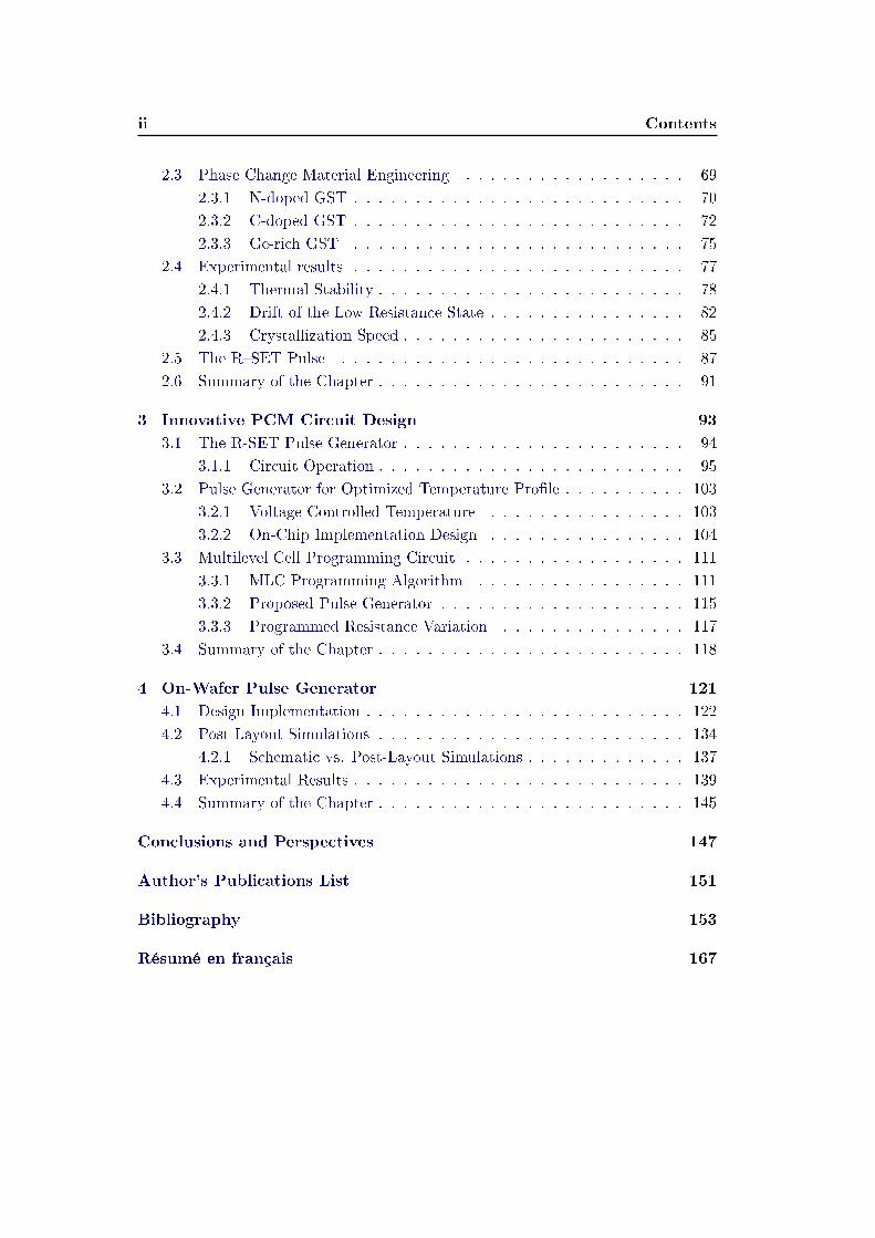
ii Contents
2.3 Phase Change Material Engineering . . . . . . . . . . . . . . . . . . 69
2.3.1 N-doped GST . . . . . . . . . . . . . . . . . . . . . . . . . . . 70
2.3.2 C-doped GST . . . . . . . . . . . . . . . . . . . . . . . . . . . 72
2.3.3 Ge-rich GST . . . . . . . . . . . . . . . . . . . . . . . . . . . 75
2.4 Experimental results . . . . . . . . . . . . . . . . . . . . . . . . . . . 77
2.4.1 Thermal Stability . . . . . . . . . . . . . . . . . . . . . . . . . 78
2.4.2 Drift of the Low Resistance State . . . . . . . . . . . . . . . . 82
2.4.3 Crystallization Speed . . . . . . . . . . . . . . . . . . . . . . . 85
2.5 The RSET Pulse . . . . . . . . . . . . . . . . . . . . . . . . . . . . 87
2.6 Summary of the Chapter . . . . . . . . . . . . . . . . . . . . . . . . . 91
3 Innovative PCM Circuit Design 93
3.1 The R-SET Pulse Generator . . . . . . . . . . . . . . . . . . . . . . . 94
3.1.1 Circuit Operation . . . . . . . . . . . . . . . . . . . . . . . . . 95
3.2 Pulse Generator for Optimized Temperature Prole . . . . . . . . . . 103
3.2.1 Voltage Controlled Temperature . . . . . . . . . . . . . . . . 103
3.2.2 On-Chip Implementation Design . . . . . . . . . . . . . . . . 104
3.3 Multilevel Cell Programming Circuit . . . . . . . . . . . . . . . . . . 111
3.3.1 MLC Programming Algorithm . . . . . . . . . . . . . . . . . 111
3.3.2 Proposed Pulse Generator . . . . . . . . . . . . . . . . . . . . 115
3.3.3 Programmed Resistance Variation . . . . . . . . . . . . . . . 117
3.4 Summary of the Chapter . . . . . . . . . . . . . . . . . . . . . . . . . 118
4 On-Wafer Pulse Generator 121
4.1 Design Implementation . . . . . . . . . . . . . . . . . . . . . . . . . . 122
4.2 Post-Layout Simulations . . . . . . . . . . . . . . . . . . . . . . . . . 134
4.2.1 Schematic vs. Post-Layout Simulations . . . . . . . . . . . . . 137
4.3 Experimental Results . . . . . . . . . . . . . . . . . . . . . . . . . . . 139
4.4 Summary of the Chapter . . . . . . . . . . . . . . . . . . . . . . . . . 145
Conclusions and Perspectives 147
Author's Publications List 151
Bibliography 153
Résumé en français 167
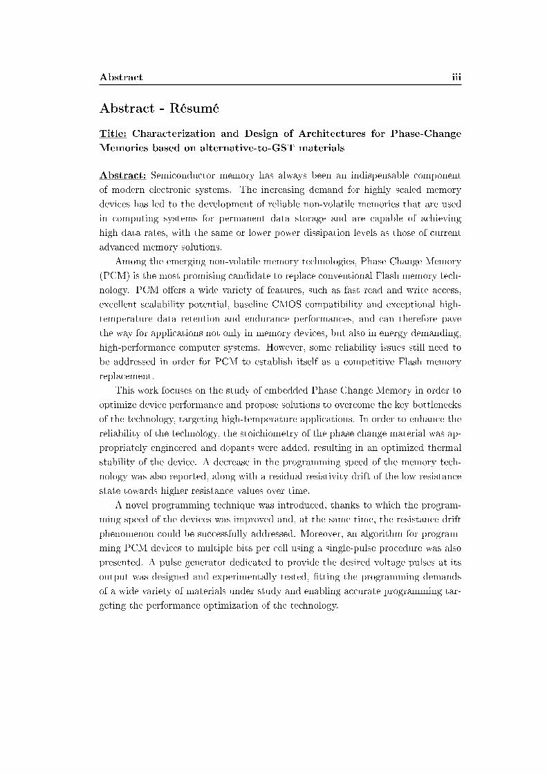
Abstract iii
Abstract - Résumé
Title: Characterization and Design of Architectures for Phase-Change
Memories based on alternative-to-GST materials
Abstract: Semiconductor memory has always been an indispensable component
of modern electronic systems. The increasing demand for highly scaled memory
devices has led to the development of reliable non-volatile memories that are used
in computing systems for permanent data storage and are capable of achieving
high data rates, with the same or lower power dissipation levels as those of current
advanced memory solutions.
Among the emerging non-volatile memory technologies, Phase Change Memory
(PCM) is the most promising candidate to replace conventional Flash memory tech-
nology. PCM oers a wide variety of features, such as fast read and write access,
excellent scalability potential, baseline CMOS compatibility and exceptional high-
temperature data retention and endurance performances, and can therefore pave
the way for applications not only in memory devices, but also in energy demanding,
high-performance computer systems. However, some reliability issues still need to
be addressed in order for PCM to establish itself as a competitive Flash memory
replacement.
This work focuses on the study of embedded Phase Change Memory in order to
optimize device performance and propose solutions to overcome the key bottlenecks
of the technology, targeting high-temperature applications. In order to enhance the
reliability of the technology, the stoichiometry of the phase change material was ap-
propriately engineered and dopants were added, resulting in an optimized thermal
stability of the device. A decrease in the programming speed of the memory tech-
nology was also reported, along with a residual resistivity drift of the low resistance
state towards higher resistance values over time.
A novel programming technique was introduced, thanks to which the program-
ming speed of the devices was improved and, at the same time, the resistance drift
phenomenon could be successfully addressed. Moreover, an algorithm for program-
ming PCM devices to multiple bits per cell using a single-pulse procedure was also
presented. A pulse generator dedicated to provide the desired voltage pulses at its
output was designed and experimentally tested, tting the programming demands
of a wide variety of materials under study and enabling accurate programming tar-
geting the performance optimization of the technology.
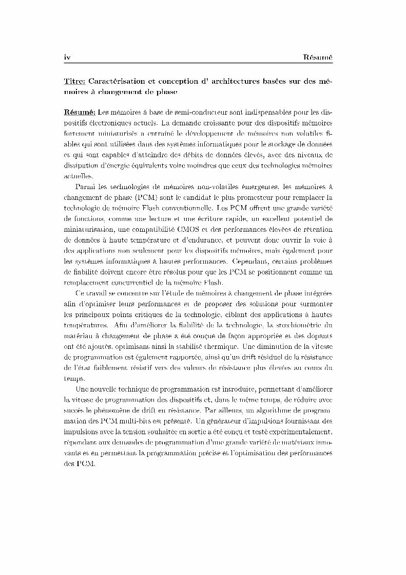
iv Résumé
Titre: Caractérisation et conception d' architectures basées sur des mé-
moires à changement de phase
Résumé: Les mémoires à base de semi-conducteur sont indispensables pour les dis-
positifs électroniques actuels. La demande croissante pour des dispositifs mémoires
fortement miniaturisés a entraîné le développement de mémoires non volatiles -
ables qui sont utilisées dans des systèmes informatiques pour le stockage de données
et qui sont capables d'atteindre des débits de données élevés, avec des niveaux de
dissipation d'énergie équivalents voire moindres que ceux des technologies mémoires
actuelles.
Parmi les technologies de mémoires non-volatiles émergentes, les mémoires à
changement de phase (PCM) sont le candidat le plus prometteur pour remplacer la
technologie de mémoire Flash conventionnelle. Les PCM orent une grande variété
de fonctions, comme une lecture et une écriture rapide, un excellent potentiel de
miniaturisation, une compatibilité CMOS et des performances élevées de rétention
de données à haute température et d'endurance, et peuvent donc ouvrir la voie à
des applications non seulement pour les dispositifs mémoires, mais également pour
les systèmes informatiques à hautes performances. Cependant, certains problèmes
de abilité doivent encore être résolus pour que les PCM se positionnent comme un
remplacement concurrentiel de la mémoire Flash.
Ce travail se concentre sur l'étude de mémoires à changement de phase intégrées
an d'optimiser leurs performances et de proposer des solutions pour surmonter
les principaux points critiques de la technologie, ciblant des applications à hautes
températures. An d'améliorer la abilité de la technologie, la st÷chiométrie du
matériau à changement de phase a été conçue de façon appropriée et des dopants
ont été ajoutés, optimisant ainsi la stabilité thermique. Une diminution de la vitesse
de programmation est également rapportée, ainsi qu'un drift résiduel de la résistance
de l'état faiblement résistif vers des valeurs de résistance plus élevées au cours du
temps.
Une nouvelle technique de programmation est introduite, permettant d'améliorer
la vitesse de programmation des dispositifs et, dans le même temps, de réduire avec
succès le phénomène de drift en résistance. Par ailleurs, un algorithme de program-
mation des PCM multi-bits est présenté. Un générateur d'impulsions fournissant des
impulsions avec la tension souhaitée en sortie a été conçu et testé expérimentalement,
répondant aux demandes de programmation d'une grande variété de matériaux inno-
vants et en permettant la programmation précise et l'optimisation des performances
des PCM.
Acknowledgements
First of all, I would like to thank my supervisor Luca Perniola for giving me the
opportunity to work in CEA-LETI for the past three years. Having his trust and
condence pushed me and motivated me to work hard and thanks to him, I got the
opportunity to work in a great scientic environment, on a topic that I ended up
loving. This period was one of the best of my life, making me better on a personal
and a professional level, and this would have not been possible without him putting
his trust in me.
I would also like to thank my thesis directors, Fabien Clermidy and Guido Torelli
for their collaboration and their scientic input. Alessandro Cabrini, my tutor
during my stay in Pavia, is another person I am feeling grateful towards, as well
as Olivier Thomas, who guided me during my short collaboration with the memory
design team of DACLE.
Besides my ocial supervisors, the biggest thank you should be given to my
behind-the-scenes supervisor, dear friend and colleague, Gabriele Navarro. I'd like
to thank him for always standing next to me, not only professionally, but also
personally. Always eager to help me and encourage me for the best, he transmitted
his warmth and passion for what he was doing, and I am truly grateful I got to work
by his side, learn so many things from him and get to know him on a personal level.
Of course I also need to thank my friends for their support and the great times
we had together. The old ones, Thilo and Natalija, who I was super lucky to end
up working together with and are practically family to me, but also a bunch of
new ones, I met in Grenoble and in Pavia, such as Cécile, Daniele, Davide, Erika,
Giorgio, Hadi, (best oce mate I could ever imagine) Julia, Lorenzo, Marinela, Sara
and of course my beloved friend Yiota! Thank you all for stoically listening to my
complaints and for always putting a smile on my face!
There are also so many colleagues I would like to thank for their collaboration,
so hoping that I am not forgetting anyone, I would like to thank Martin, my fellow
PCM traveler since day one, Onofrio, Quentin, Thérèse, Thomas, Sarra, Boubacar,
Adam D., Issam, Vincent, Loic, Alexia, Bastien, Adam M., Alex, Giuseppe, Jérémy,
Mouhamad and Mourad for our great talks and fun times.
I would also like to thank my colleagues from the electrical characterization
lab, the people from the memory design team in DACLE, and the permanent stu
from the memory components laboratory for their collaboration and their immediate
availability every time I had questions. Last but not least, I would like to thank my
colleagues and the professors in the University in Pavia, who also gave me valuable
input when I needed help during my stay there.
Finally, I would like to thank my family for their unconditional love and support.
Η Ιθάκη σ’ έδωσε τ’ ωραίο ταξίδι,
χωρίς αυτην δεν θα ΄βγαινες στον δρόμο.
΄Αλλα δεν έχει να σε δώσει πια.
Κι αν πτωχική την βρεις, η Ιθάκη δε σε γέλασε.
΄Ετσι σοφός που έγινες, με τόση πείρα,
ήδη θα το κατάλαβες οι Ιθάκες τι σημαίνουν.
Ithaca, C. P. Cavafy (1910)
Introduction
Context
Social scientists have reached the conclusion that we are living through an era in
which the generation of wealth, the exercise of power, and the creation of cultural
codes came to depend on the technological capacity of societies and individuals, with
information technologies as the core of this capacity [1]. The way modern society
handles information, strongly depends on the technological breakthroughs, which
allowed us to process and store more information much faster than a few years ago.
The information revolution was made possible thanks to several technological
improvements in fabrication techniques from one side and to the increased under-
standing of solid-state electronics mechanisms from the other side. The invention
of the integrated circuit by J. Kilby in 1958 totally changed the world and the way
we live on it, while the ability to place a large number of electronic devices on the
same chip further allowed for the invention of the rst personal computer in 1977.
It was only a matter of time before the Internet became a free platform, gradually
connecting all personal computers in the World Wide Web.
The exponential technological development of integrated circuits followed the
well-known Moore's law, which was fairly simple in its concept: according to Moore,
the number of devices that can be integrated on a chip of xed area would double
every 12 months. This simple prediction (later amended to doubling the number of
devices every 18 - 24 months) unleashed a powerful economic cycle of investment
followed by enhanced products and innovative applications motivating even more
investment. Moore's Law has become a driving force behind dramatic reductions in
unit cost over the past few decades for memory, enabling products of higher density
and ultimately putting enormous amounts of memory in the hands of the consumer
at reduced cost [2].
Semiconductor memory has always been an indispensable component of modern
electronic systems. All familiar computing platforms, ranging from hand-held de-
vices to large supercomputers, use storage systems for storing data temporarily or
permanently, having reached TB of capacities in considerably less space and power
consumption, yet maintaining a high speed [3].
The roots of memory technologies used in modern computing systems date back
to early 1970's, when the semiconductor industry was still in its nascent stage. These
technologies include solid-state memories such as Static RAM (SRAM), Dynamic
RAM (DRAM), and EPROM, as well as mechanical memories like tape and Hard
Disk Drive (HDD).
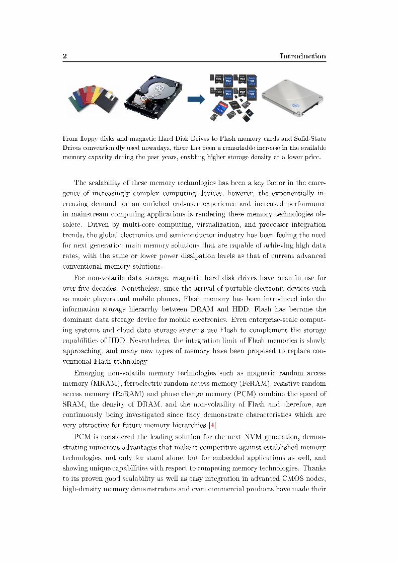
2 Introduction
From oppy disks and magnetic Hard Disk Drives to Flash memory cards and Solid-State
Drives conventionally used nowadays, there has been a remarkable increase in the available
memory capacity during the past years, enabling higher storage density at a lower price.
The scalability of these memory technologies has been a key factor in the emer-
gence of increasingly complex computing devices, however, the exponentially in-
creasing demand for an enriched end-user experience and increased performance
in mainstream computing applications is rendering these memory technologies ob-
solete. Driven by multi-core computing, virtualization, and processor integration
trends, the global electronics and semiconductor industry has been feeling the need
for next-generation main memory solutions that are capable of achieving high data
rates, with the same or lower power dissipation levels as that of current advanced
conventional memory solutions.
For non-volatile data storage, magnetic hard disk drives have been in use for
over ve decades. Nonetheless, since the arrival of portable electronic devices such
as music players and mobile phones, Flash memory has been introduced into the
information storage hierarchy between DRAM and HDD. Flash has become the
dominant data storage device for mobile electronics. Even enterprise-scale comput-
ing systems and cloud data storage systems use Flash to complement the storage
capabilities of HDD. Nevertheless, the integration limit of Flash memories is slowly
approaching, and many new types of memory have been proposed to replace con-
ventional Flash technology.
Emerging non-volatile memory technologies such as magnetic random access
memory (MRAM), ferroelectric random access memory (FeRAM), resistive random
access memory (ReRAM) and phase change memory (PCM) combine the speed of
SRAM, the density of DRAM, and the non-volatility of Flash and therefore, are
continuously being investigated since they demonstrate characteristics which are
very attractive for future memory hierarchies [4].
PCM is considered the leading solution for the next NVM generation, demon-
strating numerous advantages that make it competitive against established memory
technologies, not only for stand-alone, but for embedded applications as well, and
showing unique capabilities with respect to competing memory technologies. Thanks
to its proven good scalability as well as easy integration in advanced CMOS nodes,
high-density memory demonstrators and even commercial products have made their
Thesis Presentation 3
appearance, while the combination of small cell size and good performance, oers
Phase Change Memories the opportunity to be strongly considered for Storage Class
Memory [5] operations, in addition to embedded non-volatile memory applications.
Furthermore, as 3-D is becoming the new technological scaling paradigm, interesting
pathways to realize 3-D PCM are explored [6].
Nevertheless, some performances should be further optimized. More specically,
for stand-alone applications, a reduction of the power consumption is necessary,
while for embedded applications, the reliability of the technology has to be improved,
as well as the high-temperature data retention. Reducing the programming current
requires scaling of the active material volume, demanding new cell congurations or
concepts, while the thermal stability of the technology can be improved by proper
material engineering.
Thesis Presentation
This work focuses on the electrical characterization and the design of architectures
for Phase Change Memory based on innovative materials, targeting device perfor-
mance optimization. To this purpose, extensive electrical studies on state-of-the-art
devices have been conducted in order to understand the benets that are intro-
duced by the use of novel materials. Additionally, novel programming techniques
are investigated to deal with the problems emerging by the technology.
Chapter 1 is intended to give an overview of memory concepts that are widely
used in present memory hierarchy or are under study and are going to replace
existing memory technologies. Modern memory systems have requirements that
cannot be met by a single memory technology, thus motivating the development
of emerging device concepts that could potentially replace well-established players
in the memory market. A standard memory hierarchy is presented and existing
volatile and non-volatile memory technologies are introduced. At the end of the
Chapter, Phase Change Memory is introduced and presented in depth. The main
operation principle of the technology is discussed and the mechanisms leading to
phase transition are explained. Some of the main issues of the technology, such as
the resistivity drift are examined and potential applications for PCM are introduced.
Chapter 2 presents the electrical parameters of a PCM device, as well as the
characterization setup used in order to perform the reliability analysis, along with
the main reliability issues of PCM leading to the need for appropriate engineering of
phase change material stoichiometry in order to improve the thermal stability of our
devices. Some of the best data retention results reported in literature, in Ge-rich
based devices fabricated in the framework of the collaboration with STMicroelec-
tronics are presented. Thanks to a new programming technique, we demonstrate the
possibility to improve the programming speed of these devices and reduce the drift
4 Introduction
phenomenon that aects the resistance stability of PCM technology, in particular
at high temperature, thus proving the suitability of this particular phase change
material for embedded applications.
Chapter 3 focuses on the circuit design of architectures intended for optimized
PCM operation. Starting from the innovative programming technique introduced in
the previous Chapter, we present a pulse generator able to provide this kind of pulse
sequence. A circuit capable of generating a linearly decreasing temperature prole,
thus leading to an optimum device programming is also introduced. At the end of
the Chapter a current pulse generator capable of providing pulses for programming
the cell into multiple bits per cell is introduced and the programming algorithm
enabling Multilevel Cell programming in PCM is also examined.
Chapter 4 is dedicated to the design approach that was followed to fabricate an
on-wafer pulse generator. The analytical schematics of the circuit are presented as
well as the physical layout of the designed circuit. Schematic simulations are com-
pared to the simulations extracted from the nally laid-out circuit and the results
are in very good agreement, thus conrming the validity of the followed approach.
Finally, experimental results on silicon are provided, showing the functionality of
the fabricated circuit and its potential to be used for testing purposes.
In the end, the general conclusions of this work are provided, summarizing the
main results obtained and proposing perspectives for future research activity on
this technology, taking into consideration the performance optimization of PCM
technology introduced within the context of this study.
Chapter 1
Solid-State Memory Technologies
An ideal memory system should be fast, cheap, persistent and big (highly dense).
Until now, all memory technologies address only some of these characteristics. For
instance, Static Random Access Memory (SRAM) is very fast but also expensive,
has low density and is not persistent. Dynamic RAM (DRAM) is cheaper; however,
it is slower and not persistent as well. Disks on the other hand, are cheap, highly
dense and persistent, but are considerably slow. Flash memory lies somewhere
between DRAM and disks: it is a non-volatile memory (NVM) with higher density
than DRAM, but suers from much higher latency.
Nowadays, research is moving along three main axes for embedded memory
devices:
a) scaling down the cell size of the memory cell;
b) scaling down the operating voltage;
c) increasing the density of stored bits (and consequently reducing the cost per bit)
by using a Multilevel Cell (MLC) approach, which consists in storing more than
one bits in a single cell.
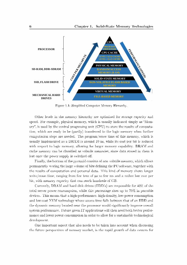
Luckily, it is possible to design a memory system that satises all the above
development trends in a single memory hierarchy. Such a hierarchy enables the
creation of a system that features fast performance, high power eciency and low
cost. More specically, this system can be implemented by a memory hierarchy
consisting of many dierent memory levels, as shown in Fig. 1.1. Memories in the
top levels of this hierarchy are faster and smaller, but have a higher cost, whereas
memories in the bottom layers are progressively larger and cheaper, but feature
considerably lower access speed.
In modern computing systems, a hierarchy of volatile and non-volatile data stor-
age devices is used in order to achieve an optimal trade-o between cost and perfor-
mance. On top of the hierarchy pyramid, we nd the portion of the memory that
is the closest to the processor core and requires frequent access (CPU registers and
cache memory). For this reason, this portion requires the fastest operation speed
possible, while it is also the most expensive due to the large chip area required.
6 Chapter 1. Solid-State Memory Technologies
VIRTUAL MEMORY
CPU
SOLID-STATE MEMORY
CPU CACHE
PHYSICAL MEMORY
REGISTERPROCESSOR
LEVEL 1 (L1) CACHELEVEL 2 (L2) CACHE
RANDOM ACCESSMEMORY (RAM)
NON-VOLATILE FLASH-BASED MEMORY
FILE-BASED MEMORY
PROCESSOR
SD-RAM, DDR-SDRAM
SSD, FLASH DRIVE
MECHANICAL HARD DRIVES
Figure 1.1: Simplied Computer Memory Hierarchy.
Other levels in the memory hierarchy are optimized for storage capacity and
speed. For example, physical memory, which is usually indicated simply as Mem-
ory, is used by the central progressing unit (CPU) to store the results of computa-
tion, which are ready to be (partly) transferred to the logic memory when further
computation steps are needed. The program/erase time of this memory, which is
usually implemented as a DRAM is around 10 ns, while its cost per bit is reduced
with respect to logic memory, allowing for larger memory capability. DRAM and
cache memory can be classied as volatile memories, since data stored in them is
lost once the power supply is switched o.
Finally, the bottom of the pyramid consists of non-volatile memory, which allows
permanently storing the large volume of bits dening the PC software, together with
the results of computation and personal data. This kind of memory shows longer
write/erase time, ranging from few tens of µs to few ms and a rather low cost per
bit, with memory capacity that can reach hundreds of GB.
Currently, DRAM and hard disk drives (HDD's) are responsible for 40% of the
total server power consumption, while this percentage rises up to 70% in portable
devices. This means that a high-performance, high-density, low-power consumption
and low-cost NVM technology whose access time falls between that of an HDD and
the dynamic memory located near the processor would signicantly improve overall
system performance. Future green IT applications will then need both better perfor-
mance and lower power consumption in order to allow for a sustainable technological
development.
One important aspect that also needs to be taken into account when discussing
the future perspectives of memory market, is the rapid growth of data centers for
1.1. Solid-State Memories - An Overview 7
cloud computing. Generally, cloud storage can provide users with immediate access
to a broad range of resources, also serving as a natural disaster-proof backup solu-
tion. The cloud computing market is predicted to see an explosive growth from a 41
billion $ market in 2011 to a 241 billion $ market in 2020. One of the key technical
bottlenecks of this novel system architecture is expected to be its storage capacity.
It is for this reason that a fast, cheap and reliable non-volatile memory technology
will be one of the most important success factors for semiconductors companies in
the near future. The main factor that will enable such changes will also be the
ability to optimize energy consumption of both giant, concentrated databases and
small, distributed portable devices.
To sustain the continuous scaling and thus be able to appear competitive in the
future, conventionally used memory devices may be obliged to undergo revolutionary
changes, since some of the limitations within each type of memory are becoming
more and more evident. Several emerging memory concepts are introduced, aiming
to go beyond those limitations and potentially replace all or most of the existing
semiconductor memory technologies and become a Universal Memory [7]. The
benet of implementing such a device would be the control of an enormous market,
which has expanded from computer applications to all kinds of consumer electronic
products [8].
In this Chapter, we introduce the reasons why memory plays a key role in mod-
ern computing systems. Thanks to the memory hierarchy used in present-day com-
puter architectures, we highlight the main requirements and specications for dif-
ferent memory technologies and present well-known memory technologies such as
SRAM, DRAM and Flash Memory, before moving on to emerging memory con-
cepts. Among the wide range of next generation memory devices covered in this
Chapter, we study the basic operation principles of Magnetoresistive Random-Access
Memory (MRAM), Ferroelectric RAM (FeRAM), Resistive Random-Access Mem-
ory (ReRAM) and Phase Change Memory (PCM). PCM is the focus of this work;
therefore, its behavior and performance are thoroughly examined.
1.1 Solid-State Memories - An Overview
Solid-state memories are a category of devices that have been developed in parallel
with logic computing. SRAM (Static Random Access Memory) and DRAM (Dy-
namic Random Access Memory) are the oldest semiconductor memories introduced
at the end of the 60's. Their main advantage is their fast access time, however, they
are volatile memories. This means that the information can be maintained only
through continuous refresh and is lost when the power supply is switched o.
8 Chapter 1. Solid-State Memory Technologies
MICROPROCESSOR
SRAM DRAMFLASH
MEMORY
OTHER NVM
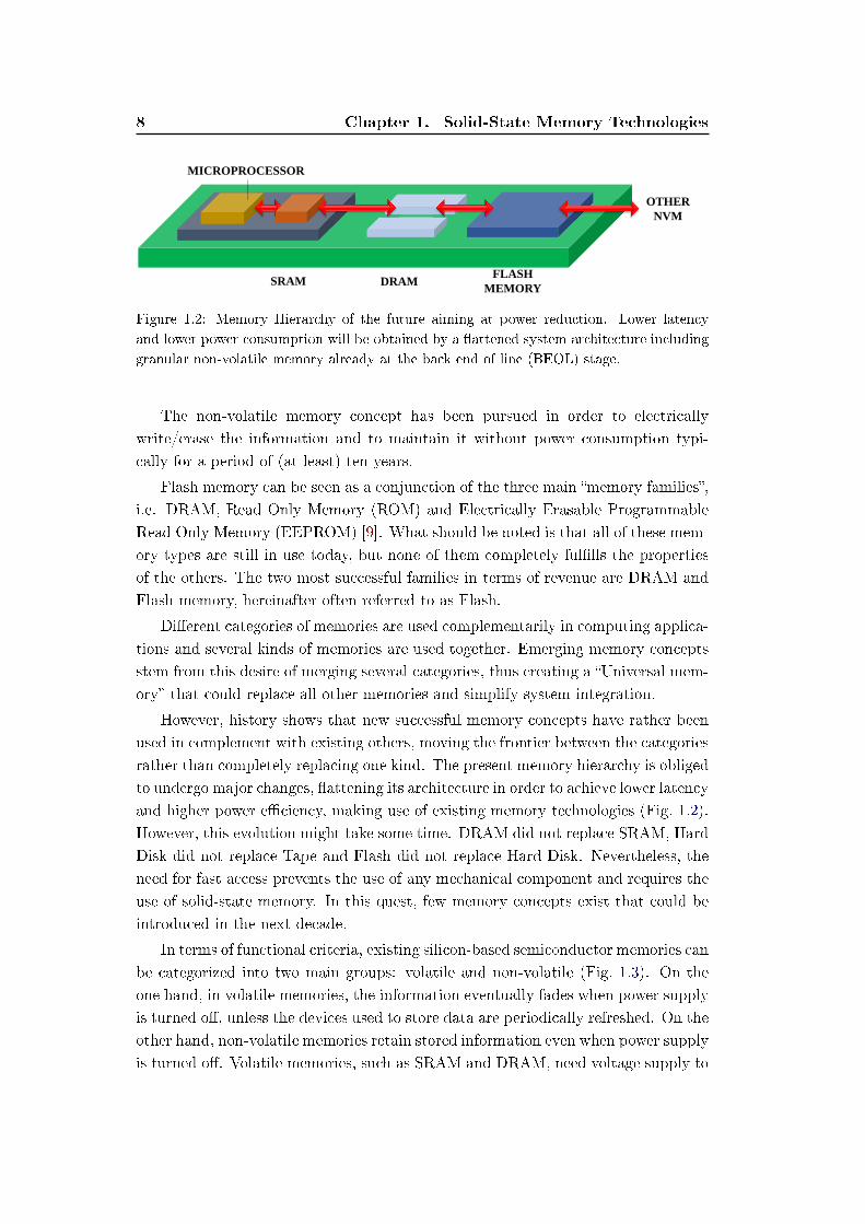
Figure 1.2: Memory Hierarchy of the future aiming at power reduction. Lower latency
and lower power consumption will be obtained by a attened system architecture including
granular non-volatile memory already at the back end of line (BEOL) stage.
The non-volatile memory concept has been pursued in order to electrically
write/erase the information and to maintain it without power consumption typi-
cally for a period of (at least) ten years.
Flash memory can be seen as a conjunction of the three main memory families,
i.e. DRAM, Read Only Memory (ROM) and Electrically Erasable Programmable
Read Only Memory (EEPROM) [9]. What should be noted is that all of these mem-
ory types are still in use today, but none of them completely fullls the properties
of the others. The two most successful families in terms of revenue are DRAM and
Flash memory, hereinafter often referred to as Flash.
Dierent categories of memories are used complementarily in computing applica-
tions and several kinds of memories are used together. Emerging memory concepts
stem from this desire of merging several categories, thus creating a Universal mem-
ory that could replace all other memories and simplify system integration.
However, history shows that new successful memory concepts have rather been
used in complement with existing others, moving the frontier between the categories
rather than completely replacing one kind. The present memory hierarchy is obliged
to undergo major changes, attening its architecture in order to achieve lower latency
and higher power eciency, making use of existing memory technologies (Fig. 1.2).
However, this evolution might take some time. DRAM did not replace SRAM, Hard
Disk did not replace Tape and Flash did not replace Hard Disk. Nevertheless, the
need for fast access prevents the use of any mechanical component and requires the
use of solid-state memory. In this quest, few memory concepts exist that could be
introduced in the next decade.
In terms of functional criteria, existing silicon-based semiconductor memories can
be categorized into two main groups: volatile and non-volatile (Fig. 1.3). On the
one hand, in volatile memories, the information eventually fades when power supply
is turned o, unless the devices used to store data are periodically refreshed. On the
other hand, non-volatile memories retain stored information even when power supply
is turned o. Volatile memories, such as SRAM and DRAM, need voltage supply to
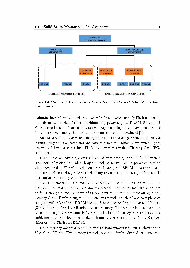
1.1. Solid-State Memories - An Overview 9
ReRAMFeRAM MRAMPCMFlash
CHARGE STORAGE
POLARITY CHANGE
RESISTANCE CHANGE
DRAMSRAM
CURRENT MEMORY DEVICES EMERGING MEMORY CONCEPTS
MEMORY TECHNOLOGIES
VOLATILE MEMORIES
NON-VOLATILE MEMORIES
Figure 1.3: Overview of the semiconductor memory classication according to their func-
tional criteria.
maintain their information, whereas non-volatile memories, namely Flash memories,
are able to hold their information without any power supply. DRAM, SRAM and
Flash are today's dominant solid-state memory technologies and have been around
for a long time. Among them, Flash is the most recently introduced [10].
SRAM is built in CMOS technology with six transistors per cell, while DRAM
is built using one transistor and one capacitor per cell, which allows much higher
density and lower cost per bit. Flash memory works with a Floating Gate (FG)
component.
DRAM has an advantage over SRAM of only needing one MOSFET with a
capacitor. Moreover, it is also cheap to produce, as well as less power consuming
when compared to SRAM, but demonstrates lower speed. SRAM is faster and easy
to control. Nevertheless, SRAM needs many transistors (is thus expensive) and is
more power consuming than DRAM.
Volatile memories consist mostly of DRAM, which can be further classied into
SDRAM. The market for DRAM devices exceeds the market for SRAM devices
by far, although a small amount of SRAM devices is used in almost all logic and
memory chips. Forthcoming volatile memory technologies that hope to replace or
compete with SRAM and DRAM include Zero-capacitor Random Access Memory
(Z-RAM), Twin-Transistor Random Access Memory (TTRAM), Advanced Random
Access Memory (A-RAM) and ETA RAM [11]. In the industry, new universal and
stable memory technologies will make their appearance as real contenders to displace
either or both Flash and DRAM.
Flash memory does not require power to store information but is slower than
SRAM and DRAM. This memory technology can be further divided into two cate-
10 Chapter 1. Solid-State Memory Technologies
gories: NOR Flash, characterized by word programming granularity and large cell
size and NAND Flash, characterized by page programming and small cell size.
Today, non-volatile memories are highly reliable and can be programmed by
using a simple microcomputer. Among them, emerging non-volatile memories and
especially Flash, have been the fastest growing segment of the semiconductor mar-
ket during the last 10 years. There are mainly ve types of non-volatile memory
technology: Flash memory, magnetic random access memory (MRAM), ferroelec-
tric random access memory (FeRAM), oxide based resistive random access memory
(ReRAM) and phase change memory (PCM).
MRAM is an NVM technology, where data is not stored in an electric charge
ow, but by magnetic storage elements. FeRAM is a random access memory similar
in construction to DRAM but uses a ferroelectric layer instead of a dielectric layer
to achieve non-volatility. ReRAM is a non-volatile memory that bases its operation
on a dielectric, normally insulating, which is made to conduct through a lament or
conduction path formed after the application of a suciently high voltage. Arguably,
this is a memristor technology and should be considered as a potentially strong
candidate to challenge NAND Flash.
Finally, PCM is a non-volatile random-access memory, based on a reversible
phase transition between the amorphous and the crystalline state of a chalcogenide
(a material that has been used to manufacture read/writable compact disks,
CD-RW's and digital versatile disks, DVD's), which is accomplished by heating
and cooling of this material.
An ideal memory device, or a so-called Universal memory, should be able to
simultaneously satisfy at least three requirements: high speed, high density and
non-volatility (retention). Up until now, such a memory device has not been devel-
oped. The oating gate non-volatile semiconductor memory has high density and
retention, but its program/erase speed is low. DRAM has high speed (access time
of approximately 10 ns) and high density, but it is volatile. In contrast, SRAM has
very high speed (access time of hundreds of ps), but its application range is limited
due to its very low density and volatility.
Researchers are in inspiring search of novel non-volatile memories, which will
successfully lead to the realization and commercialization of the Universal memory.
Among these emerging concepts, it is expected that PCM will have better scalability
than other emerging technologies. Additionally, MRAM, FeRAM and PCM are in
commercial production but still remain limited to niche applications and are many
years away from competing for industry adoption [12].
1.1. Solid-State Memories - An Overview 11
1.1.1 Static Random Access Memory - SRAM
Cache memory is employed to store frequently used information and can be placed
at several layers of the computer architecture, but probably the most important
layer is processor cache. The speed of the cache is typically inversely proportional
to its size. This means that processor cache memory needs to be very fast and small
in order to save search time.
The technology that best matches this basic set of requirements is Static Random
Access Memory. SRAM is a high-performance semiconductor memory, which is
designed using standard CMOS transistors arranged as an addressable latch. As a
memory technology, SRAM is the fastest memory in the modern hierarchy, but it
requires signicant area to implement.
An SRAM cell is generally used for instruction registers and as cache memory
in modern processors, because these elements store data that is needed and handled
immediately by the CPU. Delay in this data constitutes a direct delay in instruction
processing, so SRAM must be used for this function to ensure reasonable processor
performance.
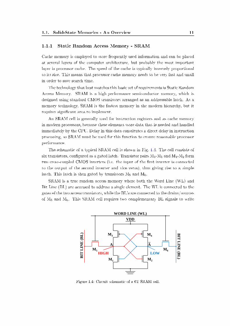
The schematic of a typical SRAM cell is shown in Fig. 1.4. The cell consists of
six transistors, congured as a gated latch. Transistor pairs M3-M1 and M4-M2 form
two cross-coupled CMOS inverters (i.e. the input of the rst inverter is connected
to the output of the second inverter and vice-versa), thus giving rise to a simple
latch. This latch is then gated by transistors M5 and M6.
SRAM is a true random access memory where both the Word Line (WL) and
Bit Line (BL) are accessed to address a single element. The WL is connected to the
gates of the two access transistors, while the BL's are connected to the drains/sources
of M5 and M6. This SRAM cell requires two complementary BL signals to write
M1 M2
M3 M4
M5 M6
VDD
BIT
LIN
E (
BL
) BIT
LIN
E (B
L)
WORD LINE (WL)
A A_
HIGH LOW
Figure 1.4: Circuit schematic of a 6T SRAM cell.
12 Chapter 1. Solid-State Memory Technologies
the cell. When the WL is high, the cell simply receives the high-low or low-high
conguration provided by the BL, which is then latched when the WL goes low.
In modern memory systems, the contribution of the inverter gate delay to the
write access time is generally less than 1 ns. In an actual SRAM, read and write
speed also depends on the distance of the memory from the arithmetic logic unit
and the time involved in the array control electronics. An SRAM array is gener-
ally integrated on the same CPU chip, which performs logic operations and thus
maintains a fast access time even at system level (in contrast to DRAM).
For instance, when used as a register, which is as close as possible to logic
computation, SRAM latency is less than 1 ns. When used as a cache, SRAM
latency at system level ranges from 1 to 20 ns. Furthermore, high speed in SRAM
is enabled by direct integration with CMOS processor logic but this is also a reason
why the maximum capacity of SRAM is limited. Considering that a state-of-the-art
microprocessor might have up to one billion transistors on a single chip and each
SRAM cell requires six transistors, as described above, we can assume that if all
transistors on the chip were used as SRAM cells, the chip itself could only constitute
a memory of a few hundred Mbit, or less than 30 MB of SRAM. This is the reason
why typical modern CPU's only have several MB of SRAM and, hence, application
memory heavily relies on DRAM.
1.1.2 Dynamic Random Access Memory - DRAM
While some of the most frequently used data are kept in cache in order to lower
access time, most of the memory addressing space used by a program is usually
stored in the main memory. Main memories have to be big enough to hold most
of the data needed by a program and can be slower than cache, since the most
frequently used data are already being cached. Since more capacity is needed, the
cost-per-bit of the main memory also needs to be lower than in the case of cache.
These requirements can be satised by Dynamic Random Access Memory.
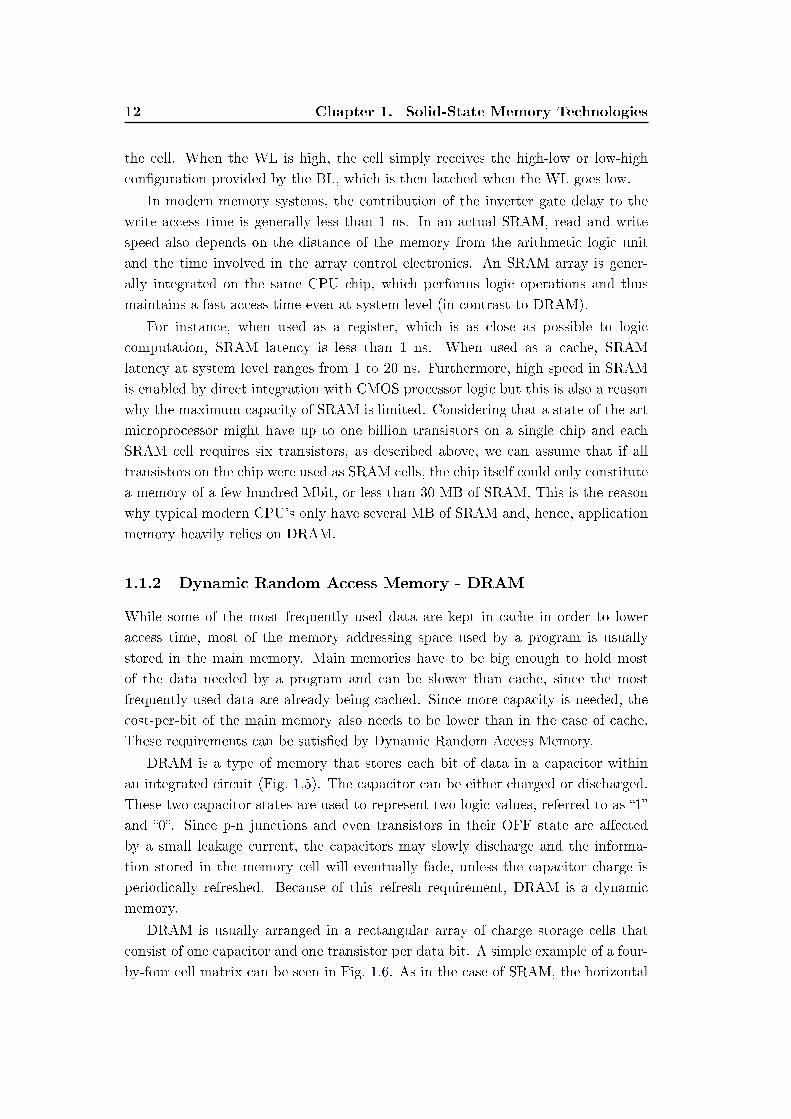
DRAM is a type of memory that stores each bit of data in a capacitor within
an integrated circuit (Fig. 1.5). The capacitor can be either charged or discharged.
These two capacitor states are used to represent two logic values, referred to as 1
and 0. Since p-n junctions and even transistors in their OFF state are aected
by a small leakage current, the capacitors may slowly discharge and the informa-
tion stored in the memory cell will eventually fade, unless the capacitor charge is
periodically refreshed. Because of this refresh requirement, DRAM is a dynamic
memory.
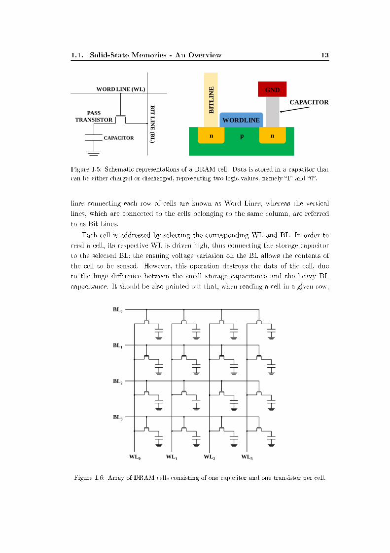
DRAM is usually arranged in a rectangular array of charge storage cells that
consist of one capacitor and one transistor per data bit. A simple example of a four-
by-four cell matrix can be seen in Fig. 1.6. As in the case of SRAM, the horizontal
1.1. Solid-State Memories - An Overview 13
PASS TRANSISTOR
WORD LINE (WL)
CAPACITOR
BIT
LIN
E (B
L)
WORDLINE
BIT
LIN
E
n np
CAPACITOR
GND
Figure 1.5: Schematic representations of a DRAM cell. Data is stored in a capacitor that
can be either charged or discharged, representing two logic values, namely 1 and 0.
lines connecting each row of cells are known as Word Lines, whereas the vertical
lines, which are connected to the cells belonging to the same column, are referred
to as Bit Lines.
Each cell is addressed by selecting the corresponding WL and BL. In order to
read a cell, its respective WL is driven high, thus connecting the storage capacitor
to the selected BL: the ensuing voltage variation on the BL allows the contents of
the cell to be sensed. However, this operation destroys the data of the cell, due
to the huge dierence between the small storage capacitance and the heavy BL
capacitance. It should be also pointed out that, when reading a cell in a given row,
BL0
BL1
BL2
BL3
WL3WL0 WL1 WL2
Figure 1.6: Array of DRAM cells consisting of one capacitor and one transistor per cell.
14 Chapter 1. Solid-State Memory Technologies
all the cells in the same row are also connected to their respective BL's and, hence,
their data are destroyed. For this reason, all the cells of the addressed WL are
read and are then written back to the level corresponding to the sensed data. This
approach is also followed to refresh a DRAM: all WL's are sequentially accessed in
order to read all the associated cells and then re-write them.
In order to store data in a cell, its respective WL is driven high and its respective
BL is driven to the desired value (high or low). The BL is held at the desired value
even when the WL voltage is removed. While performing a write operation on a
particular cell, all the columns in the selected row are sensed simultaneously and
are then re-written to the level corresponding to the sensed data.
Unlike SRAM, DRAM exhibits structural simplicity [13]. Only one transistor
and one capacitor are required to store information for one bit. This allows DRAM
to reach very high densities when compared to SRAM, where six transistors are
needed for the same amount of information. The transistors and capacitors used
are extremely small; billions can t on a single memory chip. However, despite its
numerous advantages, DRAM is a volatile memory, i.e. it is incapable of retaining
its data once power supply is removed, and its operation speed is lower than that
of SRAM.
Despite the fact that DRAM has been able to double its capacity every two
years, its latency does not follow an equally impressive improvement. Moreover,
DRAM technology is bound to hit a density wall, which will eventually result in its
replacement by emerging memory technologies, such as Spin Transfer Torque RAM
or Phase Change Memory.
1.1.3 Flash Memory
Flash memory has been conceived by Professor Fujio Masuoka in 1980 and was rst
presented in 1984. The word Flash comes from the fact that the data from a whole
memory block (referred to as sector) can be erased in one single shot. With an
electrical erase, it is possible to reprogram the read only memory in situ without
removing the memory from the system. The design of the memory was based on
a NOR array conguration (see below) and was dedicated to code storage. This
memory is commonly called NOR Flash memory. In order to decrease the cost of
Flash memory, NAND Flash memory was also invented by Professor Fujio Masuoka
in 1987. NAND Flash memory has been dedicated to data storage and is based on
a NAND array conguration.
1.1.3.1 Operation Principle
Flash Memory is based on a MOS transistor structure with a modied gate stack
(Fig. 1.7). The gate stack is composed by a poly-silicon oating gate embedded
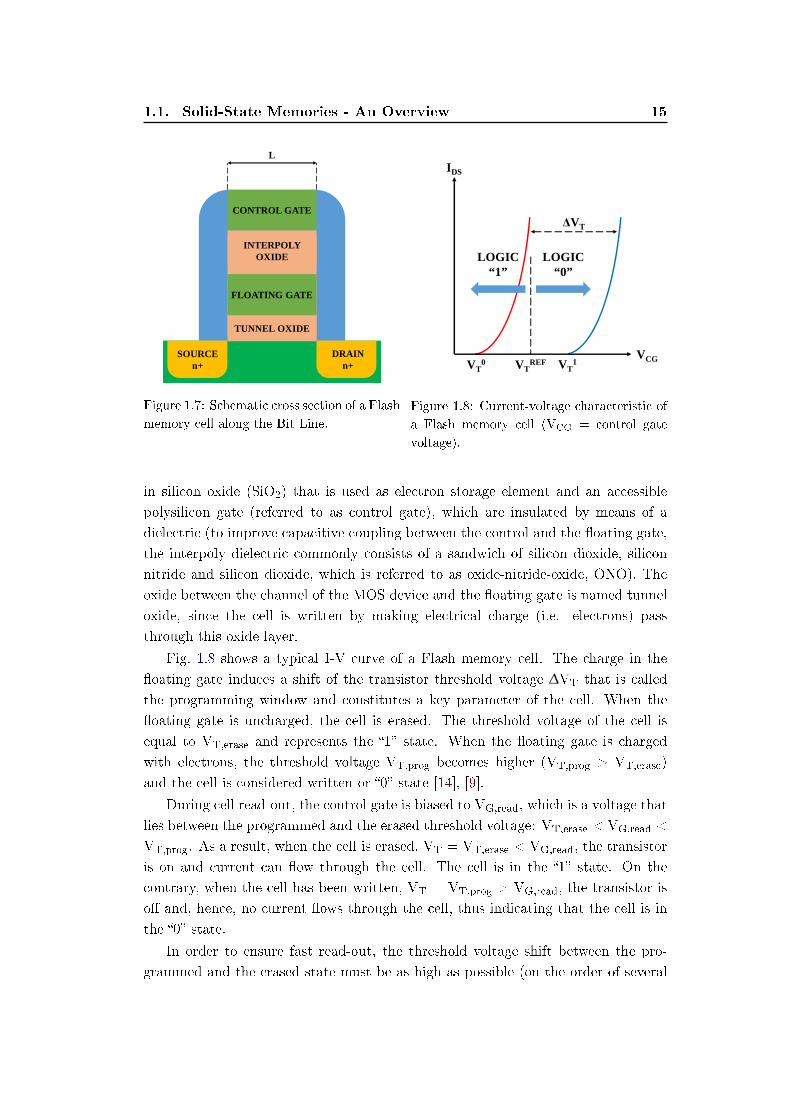
1.1. Solid-State Memories - An Overview 15
SOURCEn+
p SUBSTRATE
TUNNEL OXIDE
INTERPOLY OXIDE
FLOATING GATE
CONTROL GATE
L
DRAINn+
Figure 1.7: Schematic cross section of a Flash
memory cell along the Bit Line.
LOGIC “0”
LOGIC “1”
VCG
IDS
ΔVT
VTREFVT
0 VT1
Figure 1.8: Current-voltage characteristic of
a Flash memory cell (VCG = control gate
voltage).
in silicon oxide (SiO2) that is used as electron storage element and an accessible
polysilicon gate (referred to as control gate), which are insulated by means of a
dielectric (to improve capacitive coupling between the control and the oating gate,
the interpoly dielectric commonly consists of a sandwich of silicon dioxide, silicon
nitride and silicon dioxide, which is referred to as oxide-nitride-oxide, ONO). The
oxide between the channel of the MOS device and the oating gate is named tunnel
oxide, since the cell is written by making electrical charge (i.e. electrons) pass
through this oxide layer.
Fig. 1.8 shows a typical I-V curve of a Flash memory cell. The charge in the
oating gate induces a shift of the transistor threshold voltage ∆VT that is called
the programming window and constitutes a key parameter of the cell. When the
oating gate is uncharged, the cell is erased. The threshold voltage of the cell is
equal to VT,erase and represents the 1 state. When the oating gate is charged
with electrons, the threshold voltage VT,prog becomes higher (VT,prog > VT,erase)
and the cell is considered written or 0 state [14], [9].
During cell read-out, the control gate is biased to VG,read, which is a voltage that
lies between the programmed and the erased threshold voltage: VT,erase < VG,read <
VT,prog. As a result, when the cell is erased, VT = VT,erase < VG,read, the transistor
is on and current can ow through the cell. The cell is in the 1 state. On the
contrary, when the cell has been written, VT = VT,prog > VG,read, the transistor is
o and, hence, no current ows through the cell, thus indicating that the cell is in
the 0 state.
In order to ensure fast read-out, the threshold voltage shift between the pro-
grammed and the erased state must be as high as possible (on the order of several
16 Chapter 1. Solid-State Memory Technologies
BIT LINE
WL0 WL1 WL2 WL3 WL4 WL5 WL6 WL7
S DRAIN
p SUBSTRATE
TUNNEL OXIDE
INTERPOLY OXIDE
FLOATING GATE
CONTROL GATE
TUNNEL OXIDE
INTERPOLY OXIDE
FLOATING GATE
CONTROL GATE
SOURCE
TUNNEL OXIDE
INTERPOLY OXIDE
FLOATING GATE
CONTROL GATE
DRAIN
TUNNEL OXIDE
INTERPOLY OXIDE
FLOATING GATE
CONTROL GATE
S
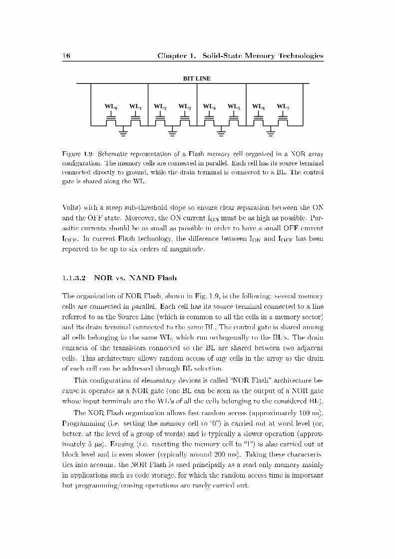
BIT LINEFigure 1.9: Schematic representation of a Flash memory cell organized in a NOR array
conguration. The memory cells are connected in parallel. Each cell has its source terminal
connected directly to ground, while the drain terminal is connected to a BL. The control
gate is shared along the WL.
Volts) with a steep sub-threshold slope to ensure clear separation between the ON
and the OFF state. Moreover, the ON current ION must be as high as possible. Par-
asitic currents should be as small as possible in order to have a small OFF current
IOFF. In current Flash technology, the dierence between ION and IOFF has been
reported to be up to six orders of magnitude.
1.1.3.2 NOR vs. NAND Flash
The organization of NOR Flash, shown in Fig. 1.9, is the following: several memory
cells are connected in parallel. Each cell has its source terminal connected to a line
referred to as the Source Line (which is common to all the cells in a memory sector)
and its drain terminal connected to the same BL. The control gate is shared among
all cells belonging to the same WL, which run orthogonally to the BL's. The drain
contacts of the transistors connected to the BL are shared between two adjacent
cells. This architecture allows random access of any cells in the array as the drain
of each cell can be addressed through BL selection.
This conguration of elementary devices is called NOR Flash architecture be-
cause it operates as a NOR gate (one BL can be seen as the output of a NOR gate
whose input terminals are the WL's of all the cells belonging to the considered BL).
The NOR Flash organization allows fast random access (approximately 100 ns).
Programming (i.e. setting the memory cell to 0) is carried out at word level (or,
better, at the level of a group of words) and is typically a slower operation (approx-
imately 5 µs). Erasing (i.e. resetting the memory cell to 1) is also carried out at
block level and is even slower (typically around 200 ms). Taking these characteris-
tics into account, the NOR Flash is used principally as a read only memory mainly
in applications such as code storage, for which the random access time is important
but programming/erasing operations are rarely carried out.
1.1. Solid-State Memories - An Overview 17
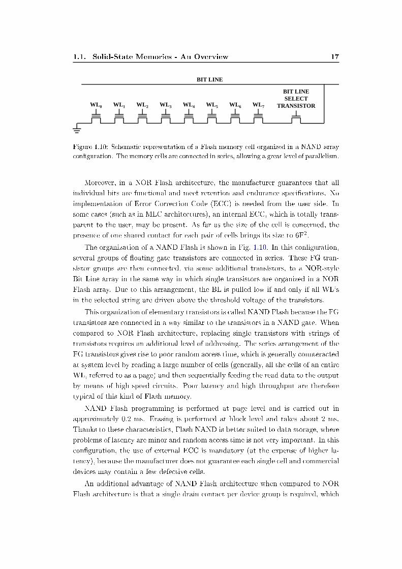
BIT LINE
BIT LINE SELECT
TRANSISTORWL0 WL1 WL2 WL3 WL4 WL5 WL6 WL7
S DRAIN
p SUBSTRATE
TUNNEL OXIDE
INTERPOLY OXIDE
FLOATING GATE
CONTROL GATE
TUNNEL OXIDE
INTERPOLY OXIDE
FLOATING GATE
CONTROL GATE
SOURCE
TUNNEL OXIDE
INTERPOLY OXIDE
FLOATING GATE
CONTROL GATE
DRAIN
TUNNEL OXIDE
INTERPOLY OXIDE
FLOATING GATE
CONTROL GATE
S
Figure 1.10: Schematic representation of a Flash memory cell organized in a NAND array
conguration. The memory cells are connected in series, allowing a great level of parallelism.
Moreover, in a NOR Flash architecture, the manufacturer guarantees that all
individual bits are functional and meet retention and endurance specications. No
implementation of Error Correction Code (ECC) is needed from the user side. In
some cases (such as in MLC architectures), an internal ECC, which is totally trans-
parent to the user, may be present. As far as the size of the cell is concerned, the
presence of one shared contact for each pair of cells brings its size to 6F2.
The organization of a NAND Flash is shown in Fig. 1.10. In this conguration,
several groups of oating gate transistors are connected in series. These FG tran-
sistor groups are then connected, via some additional transistors, to a NOR-style
Bit Line array in the same way in which single transistors are organized in a NOR
Flash array. Due to this arrangement, the BL is pulled low if and only if all WL's
in the selected string are driven above the threshold voltage of the transistors.
This organization of elementary transistors is called NAND Flash because the FG
transistors are connected in a way similar to the transistors in a NAND gate. When
compared to NOR Flash architecture, replacing single transistors with strings of
transistors requires an additional level of addressing. The series arrangement of the
FG transistors gives rise to poor random access time, which is generally counteracted
at system level by reading a large number of cells (generally, all the cells of an entire
WL, referred to as a page) and then sequentially feeding the read data to the output
by means of high-speed circuits. Poor latency and high throughput are therefore
typical of this kind of Flash memory.
NAND Flash programming is performed at page level and is carried out in
approximately 0.2 ms. Erasing is performed at block level and takes about 2 ms.
Thanks to these characteristics, Flash NAND is better suited to data storage, where
problems of latency are minor and random access time is not very important. In this
conguration, the use of external ECC is mandatory (at the expense of higher la-
tency), because the manufacturer does not guarantee each single cell and commercial
devices may contain a few defective cells.
An additional advantage of NAND Flash architecture when compared to NOR
Flash architecture is that a single drain contact per device group is required, which
18 Chapter 1. Solid-State Memory Technologies
allows reaching an optimal cell size of 4F2 and, hence, a 30% area gain with respect
to a NOR Flash array, resulting in higher density.
Many of the advantages and disadvantages of NOR and NAND Flash devices
arise directly from the dierences in the architecture used for their implementation.
Not surprisingly, the names for these two technologies carry a signicant clue as to
the implementation dierences [15]. The extra connections used in the NOR archi-
tecture provide some additional exibility when compared to NAND conguration,
whereas NAND devices have a simpler and more silicon-ecient layout than NOR
devices due to their series structure as well as the smaller number of ground wires
and BL's with respect to NOR devices.
Both NOR and NAND Flash memory devices push density even further by
storing more than one data bit per cell. Multilevel cell devices store two bits per
cell by trapping four dierent levels of charge in the storage cell, thus establishing
four dierent threshold voltages. Nevertheless, more complex read and write circuits
as well as more complex error management algorithms are required when storing
multiple bits per cell. On the other hand, the overall benet in cost per bit typically
outweighs the added complexity and reduced performance that comes with more
advanced management techniques.
1.1.3.3 Main Issues and Perspectives
While Flash memory has enabled the emergence of a wide range of consumer prod-
ucts, it does not fulll all requirements to establish itself as a Universal Memory.
The main limitations are read bandwidth for NAND Flash and write bandwidth for
NOR Flash. The speed gap of Flash with respect to DRAM is still large, while its
endurance is limited to 106 cycles. The high voltage needed for the operation of the
cell is also a strong limitation for future interfacing with leading edge CMOS tech-
nology. As a result, other candidates are expected to replace Flash memory. Some
of them (MRAM, FeRAM, PCM) are already used in niche market, whereas others
(ReRAM) have promising characteristics and are slowly starting their introduction
in the memory market (ReRAM).
Even though these new technologies usually require the introduction of new
materials and device architectures that prevent direct competition with the low-
price and reliable materials of standard Flash technology, the inability of Flash to
scale below the 20 nm node renders the development of these new memory concepts
necessary in order to eciently replace Flash and establish themselves as potential
Storage Class Memory candidates [5].
In the following paragraphs, several replacement solutions of Flash memory are
investigated. Herewith are presented MRAM, FeRAM, ReRAM and PCM. These
technologies are investigated for code storage operations in order to replace the NOR
1.1. Solid-State Memories - An Overview 19
MAGNETIC FIELD
CURRENT
DIGITLINE
BIT LINE
FREE LAYER
HARD LAYER
OXIDE LAYER
CURRENT SELECTOR
MTJ
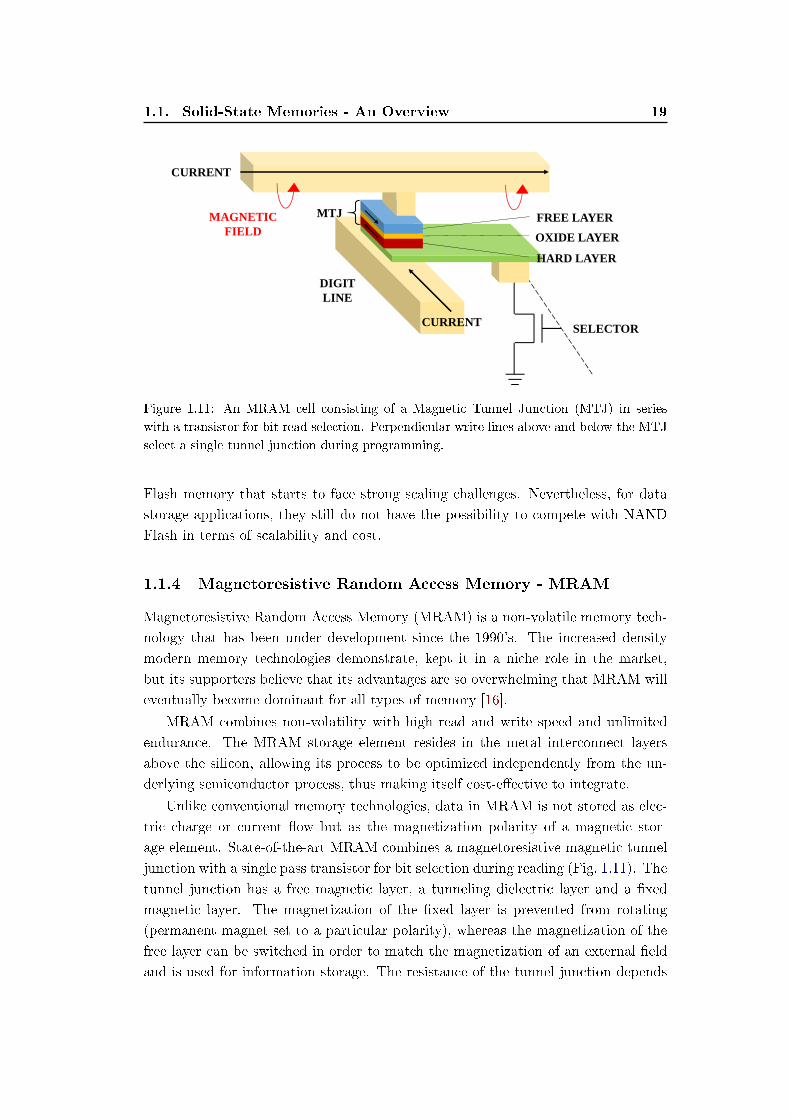
Figure 1.11: An MRAM cell consisting of a Magnetic Tunnel Junction (MTJ) in series
with a transistor for bit read selection. Perpendicular write lines above and below the MTJ
select a single tunnel junction during programming.
Flash memory that starts to face strong scaling challenges. Nevertheless, for data
storage applications, they still do not have the possibility to compete with NAND
Flash in terms of scalability and cost.
1.1.4 Magnetoresistive Random Access Memory - MRAM
Magnetoresistive Random Access Memory (MRAM) is a non-volatile memory tech-
nology that has been under development since the 1990's. The increased density
modern memory technologies demonstrate, kept it in a niche role in the market,
but its supporters believe that its advantages are so overwhelming that MRAM will
eventually become dominant for all types of memory [16].
MRAM combines non-volatility with high read and write speed and unlimited
endurance. The MRAM storage element resides in the metal interconnect layers
above the silicon, allowing its process to be optimized independently from the un-
derlying semiconductor process, thus making itself cost-eective to integrate.
Unlike conventional memory technologies, data in MRAM is not stored as elec-
tric charge or current ow but as the magnetization polarity of a magnetic stor-
age element. State-of-the-art MRAM combines a magnetoresistive magnetic tunnel
junction with a single pass transistor for bit selection during reading (Fig. 1.11). The
tunnel junction has a free magnetic layer, a tunneling dielectric layer and a xed
magnetic layer. The magnetization of the xed layer is prevented from rotating
(permanent magnet set to a particular polarity), whereas the magnetization of the
free layer can be switched in order to match the magnetization of an external eld
and is used for information storage. The resistance of the tunnel junction depends
20 Chapter 1. Solid-State Memory Technologies
on the relative magnetization orientation of the free layer with respect to that of
a xed layer, being much lower when the two layers have the same magnetization
polarity. This conguration is known as a spin valve and is the simplest structure
for an MRAM cell.
Reading is accomplished by measuring the electrical resistance of the cell. Be-
cause of the magnetic tunnel eect, the electrical resistance of the cell changes due to
the orientation of the elds in the two magnetic plates. The magnetization polarity
of the writable plane and, consequently, the resistance of the cell can be determined
by measuring the resulting current through the cell, when a bias of approximately
0.3 V is applied. Typically, if the two plates have the same polarity (larger elec-
tric current through the cell), we have a logic 1, while in the case of the opposite
polarity, the measured current is higher and we have a logic 0.
MRAM has similar performance to SRAM, similar density to DRAM (with a
much lower power consumption), is faster and suers no degradation in time when
compared to Flash memory. This combination of characteristics makes it a good
candidate for a Universal Memory, able to replace SRAM, DRAM, EEPROM and
Flash. A huge amount of research is carried out into developing it, however, MRAM
still has to face several challenges before it can be introduced to the market on a
large scale.
One of these challenges relates to the switching current distribution. The write
selection scheme that is conventionally used in MRAM requires tight and uniform
switching current distributions, which cannot be always achieved. Another current-
related concern for MRAM is its relatively small read-out signal, which eectively
limits its read speed.
As with any new memory technology, the most obvious concerns relate to the
long-term stability of memory device elements and characteristics, such as the ultra
thin tunneling barrier, the stability of the magnetic layers in the free layer and data
retention. Accelerated tests show that these mechanisms have negligible impact on
memory performance at operating conditions. In particular, the tunneling barrier
is likely to be highly stable, because aluminum oxide has a high breakdown voltage
even at very small thicknesses, MRAM uses a low operating voltage and only the
magnetic tunnel junctions that are being read are subject to voltage stress.
Future generations of MRAM will use smaller tunnel junctions and will thus have
to re-address the above challenges. Nevertheless, going towards smaller dimensions
should not introduce more bit-to-bit variations or jeopardize data retention. The
switching current will not increase with reduced bit size, however, the current density
will scale inversely with the conductor area and electromigration may therefore
become an issue. At that point, spin momentum transfer (magnetization polarity
switching by a spin-polarized current) might become a viable alternative to 2-D
write selection.
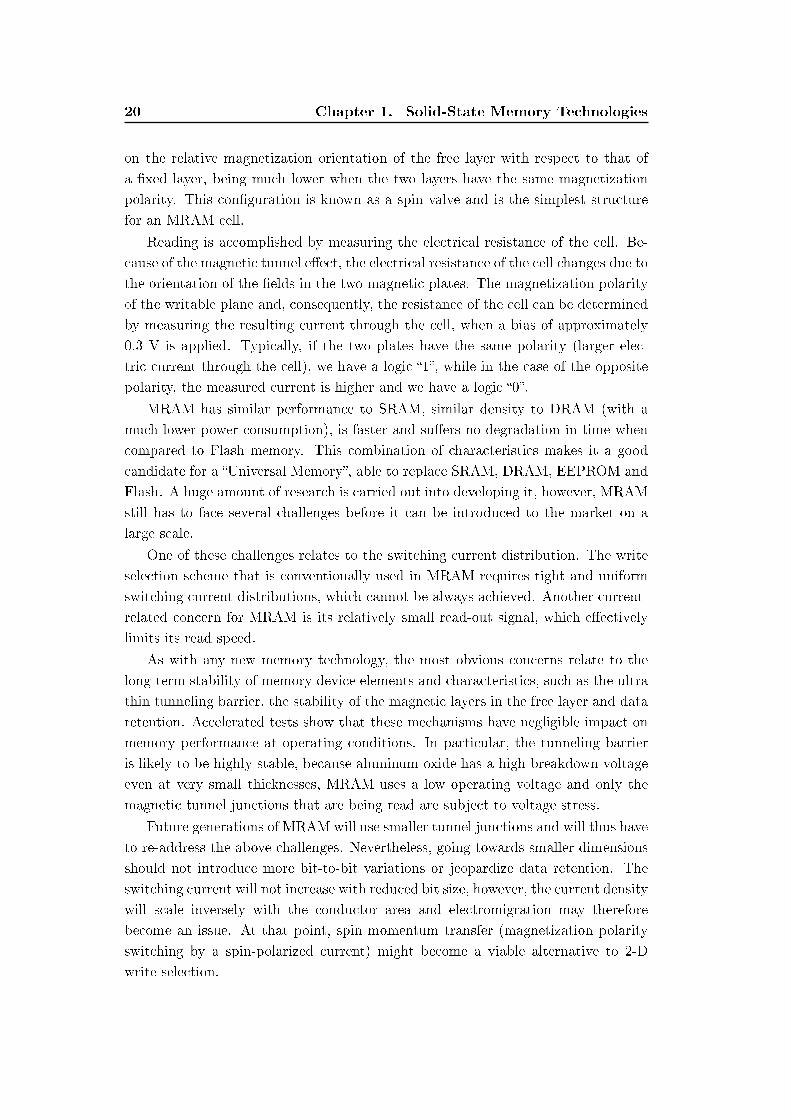
1.1. Solid-State Memories - An Overview 21
WORDLINE
FERROELECTRIC
BIT
LIN
E
n npFERROELECTRIC
BIT
LIN
E
WORDLINE(a) (b)
Figure 1.12: Schematic representation (a) and cross section (b) of a FeRAM cell. FeRAM is
similar in structure to DRAM and uses ferroelectric lms instead of a conventional capacitor
to store information.
1.1.5 Ferroelectric Random Access Memory - FeRAM
FeRAM (Ferroelectric Random Access Memory) is a high-performance and low-
power non-volatile memory that combines the benets of conventional non-volatile
memories (Flash and EEPROM) and high-speed RAM (SRAM and DRAM). This
memory technology outperforms existing memories like EEPROM and Flash, is less
power-consuming and much faster and has greater endurance to multiple read and
write operations [17].
FeRAM is similar in structure to DRAM but uses a ferroelectric layer instead of
a dielectric one to achieve non-volatility, as can be seen in Fig. 1.12. The FeRAM
cell structure, which is similar to the transistor and capacitor structure of a DRAM
cell, does not require the same high programming voltages as Flash. By using
the polarization of a ferroelectric lm material placed between two electrodes, it
is possible to store information, oering non-volatile data storage, while still being
signicantly more energy-ecient when compared with conventional memory tech-
nologies. Moreover, it oers the same functionality as Flash memory and some of
its advantages include lower power consumption, fast read/write performance and
an essentially unlimited endurance (reaching up to 1012 cycles).
FeRAM uses ferroelectric lms as a capacitor for storing data. Ferroelectric ma-
terials exhibit a non-linear relationship between the applied electric eld and the
stored charge. More specically, the characteristic of ferroelectric materials has the
form of a hysteresis loop, which is similar to the hysteresis loop of ferromagnetic ma-
terials. The dielectric constant of a ferroelectric material is typically much higher
than that of a linear dielectric because of the eects of semi-permanent electric
dipoles formed in the crystal structure of the material. When an external electric
eld is applied to a dielectric, the dipoles tend to align themselves with the eld
direction, producing small shifts in the positions of atoms and, hence, in the dis-
tributions of electronic charge in the crystal structure. After the applied voltage is
22 Chapter 1. Solid-State Memory Technologies
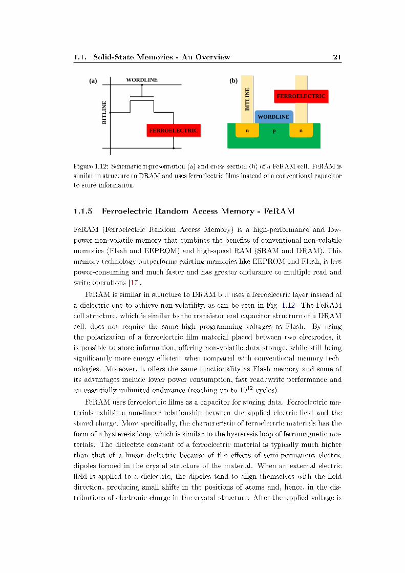
Figure 1.13: PZT (PbZr,TiO3), which has a perovskite-type structure (ABO3), is com-
monly used in ferroelectric memory. When an electric eld is applied, Zr/Ti atoms shift up
or down (depending on the eld polarity) and this polarization remains when the electric
eld is removed.
removed, the dipoles retain their polarization state. Bits are stored as one of two
possible electric polarizations in each data storage cell.
In FeRAM applications, PZT (PbZr,TiO3), which has a perovskite-type struc-
ture (ABO3), is commonly used [18]. When an electric eld is applied, the Zr/Ti
atom shifts up or down and this polarization remains once the electric eld is re-
moved (Fig. 1.13). This material property provides non-volatility and keeps the
power required for data storage low.
In terms of programming, FeRAM is similar to DRAM. Writing is accomplished
by applying a voltage across the ferroelectric layer and, hence, forcing the atoms
inside into the up or down orientation (depending on the polarity of the applied
voltage), thereby storing a 1 or a 0. Reading, however, is dierent than in DRAM.
The cell is forced into a particular state: if the cell was already programmed to a
state similar to the one it is forced to, nothing will happen in the output lines.
If the cell was programmed in the opposite state, the re-orientation of the atoms
in the ferroelectric lm will cause a brief pulse of current in the output lines, as
electrons are pushed out of the metal towards the electrode contacts. Since this
process overwrites the cell, reading FeRAM is a destructive process and requires the
cell to be re-written to the original state if the information stored in it is altered.
Texas Instruments proved that it is possible to embed FeRAM cells in a CMOS
fabrication process using two additional masking steps. Flash typically requires nine
masks. This enables for example, the integration of FeRAM on micro-controllers,
where a simplied process would reduce cost. However, the materials used to make
FeRAM are not commonly used in CMOS integrated circuit manufacturing. Both
the PZT ferroelectric layer and the noble metals used for electrodes raise CMOS
process compatibility and contamination issues.
However, the storage density FeRAM demonstrates is much lower than that of
Flash memory and, therefore, its fabrication cost is much higher. Flash memory
cells can store multiple bits per cell (up to three in the highest density NAND
Flash devices) and for this reason the areal bit density of Flash memory is much
1.1. Solid-State Memories - An Overview 23
higher with respect to FeRAM, bringing the cost per bit of Flash memory orders of
magnitude below that of FeRAM. The density of FeRAM arrays might be increased
by improvements in FeRAM fabrication process ow and cell structures, such as the
development of vertical capacitor structures (the same way as for DRAM) to reduce
the area of the cell footprint.
1.1.6 Resistive Random Access Memory - ReRAM
The last technology alternative presented here is Resistive RAM (ReRAM). Non-
volatility is based on the reversible breakdown of an oxide. This technology is
still at a research stage. The memory device consists of a resistance-changeable
material sandwiched by two terminal electrodes. Resistance change can be achieved
by applying controlled current or voltage pulses to the electrodes. The resistance
state remains stable with no need for refresh.
Up to date, a number of dierent switching characteristics have been observed
in a variety of material systems, which include NiO2, TiO2, HfO2, WOx, CuOx and
TaOx. In fact, it has become understood that a number of combinations of an oxide
with metal electrodes can exhibit some kind of resistance switching behavior [19].
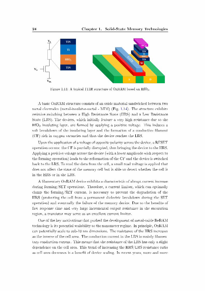
Two main classes of ReRAM, based on dierent mechanisms, exist: OxRAM
based on metallic lament formation and CBRAM based on ionic conduction. Oxide-
based RAM is the object of research by companies such as Fujitsu, Samsung,
Macronix, Panasonic, Sharp, STMicroelectronics, SMIC and TSMC. CB-RAM is
(or has been) the object of research by companies such as Qimonda, Micron, Sam-
sung and Sony.
1.1.6.1 Oxide-based Resistive Random Access Memories - OxRAM
Resistive switching refers to the physical phenomenon where a dielectric suddenly
changes its resistance under the application of an electric eld or current. This
resistance change is non-volatile and reversible. Typical resistive switching systems
are capacitor-like devices, where the electrode is an ordinary metal and the dielec-
tric a transition metal oxide. An interesting application of resistive switching is
the fabrication of novel non-volatile oxide-based resistive random access memories
(OxRAM). This eect also represents the base of the operation of the so-called
memristor devices [20] and neuromorphic memory applications [21].
OxRAM is expected to be a memory technology that can bring a revolution in
memory hierarchy and system architecture, since it can be integrated with conven-
tional CMOS in a simple way and presents a lot of advantages, such as low cost,
BEOL compatibility, non-volatility with high-speed, bit-alterable read/write, good
endurance and potentially low power/energy consumption.
24 Chapter 1. Solid-State Memory Technologies
TiN
TiN
Ti
HfO2
VG
VBL
VA
TiN
TiNTi
HfO2
AlCu
W
S D
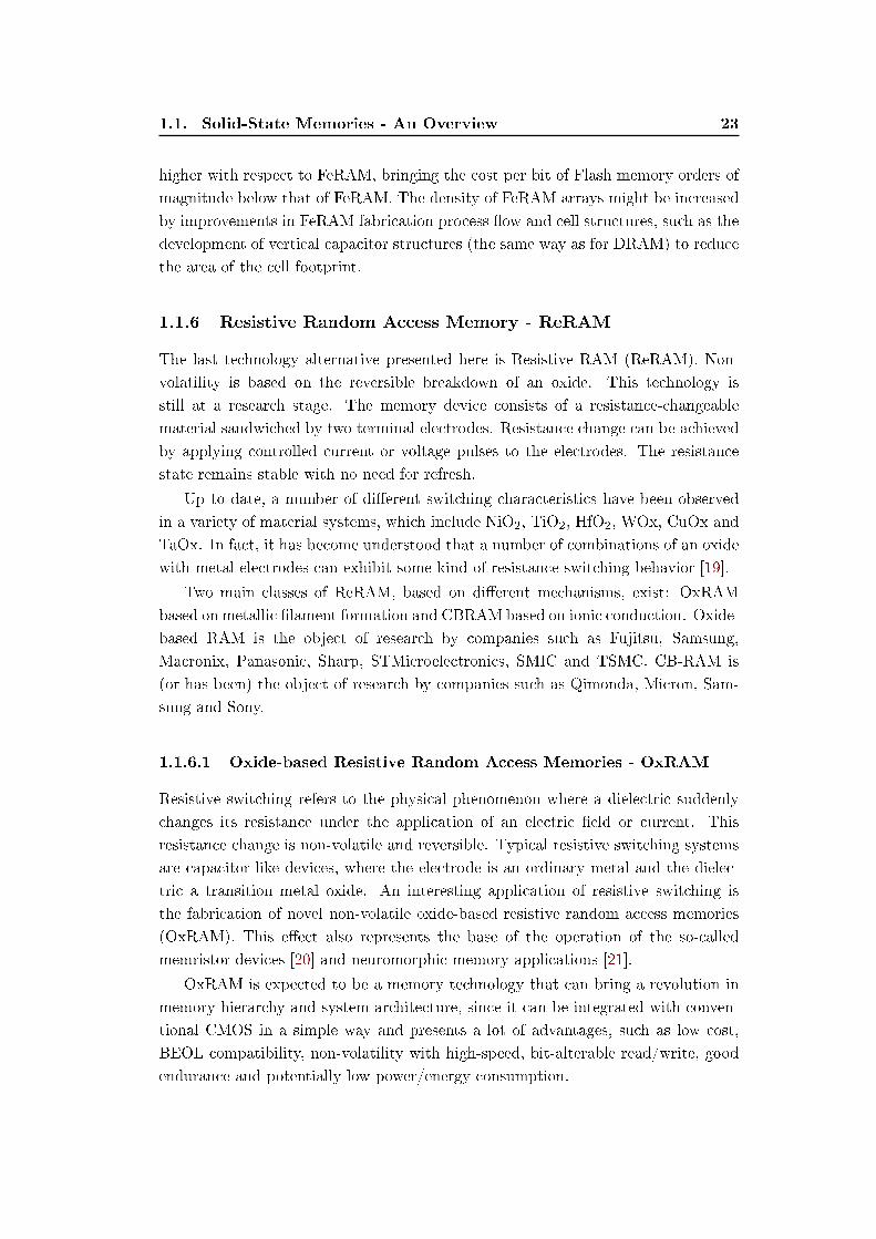
Figure 1.14: A typical 1T1R structure of OxRAM based on HfO2.
A basic OxRAM structure consists of an oxide material sandwiched between two
metal electrodes (metal-insulator-metal - MIM) (Fig. 1.14). The structure exhibits
resistive switching between a High Resistance State (HRS) and a Low Resistance
State (LRS). The devices, which initially feature a very high resistance due to the
HfO2 insulating layer, are formed by applying a positive voltage. This induces a
soft breakdown of the insulating layer and the formation of a conductive lament
(CF) rich in oxygen vacancies and thus the device reaches the LRS.
Upon the application of a voltage of opposite polarity across the device, a RESET
operation occurs: the CF is partially disrupted, thus bringing the device to the HRS.
Applying a positive voltage across the device (with a lower amplitude with respect to
the forming operation) leads to the reformation of the CF and the device is switched
back to the LRS. To read the data from the cell, a small read voltage is applied that
does not aect the state of the memory cell but is able to detect whether the cell is
in the HRS or in the LRS.
A lamentary OxRAM device exhibits a characteristic of abrupt current increase
during forming/SET operations. Therefore, a current limiter, which can optimally
clamp the forming/SET current, is necessary to prevent the degradation of the
HRS (protecting the cell from a permanent dielectric breakdown during the SET
operation) and eventually the failure of the memory device. Due to the benets of
fast response time and very large incremental output resistance in the saturation
region, a transistor may serve as an excellent current limiter.
One of the key motivations that pushed the development of metal-oxide ReRAM
technology is its potential scalability to the nanometer regime. In principle, OxRAM
can potentially scale to sub-10 nm dimensions. The resistance of the HRS increases
as the inverse of the cell area. The conduction current in the LRS is mainly lamen-
tary conduction current. This means that the resistance of the LRS has only a slight
dependence on the cell area. This trend of increasing the HRS/LRS resistance ratio
as cell area decreases is a benet of device scaling. In recent years, more and more
1.1. Solid-State Memories - An Overview 25
ELECTRODE
ELECTRODE
ELECTRODE
ELECTRODE
Ag-RICH PRECIPITATES
METAL+ IONS
ELECTRONS
+
+-
-
OFF STATEON STATEFigure 1.15: Schematic illustration of the CBRAM switching mechanism. In order to
achieve the ON state, a redox reaction drives Ag ions into the electrolyte, which results in a
conductive bridge. When programming the cell to the OFF state, the size and the number
of the Ag-rich clusters is reduced, thus breaking the conductive bridge [24].
metal-oxide memory devices with sub-100 nm feature size have been fabricated by
either optical or e-beam lithography.
Nevertheless, one of the major barriers to large-scale manufacturing of OxRAM
is the poor uniformity of device characteristics. Signicant parameter uctuations
exist in terms of variation of the switching voltages as well as of the HRS and LRS
resistance values. The variations of the resistance switching include temporal (cycle
to cycle) and spatial uctuations (device to device). The origin of these variations
may be attributed to the stochastic nature of oxygen vacancies generation [22]. The
LRS resistance variation comes from the variation of the number or the size of CF's,
thus the reduction of possible lament paths eectively connes the active switching
region and leads to a reduction of the LRS variation. The HRS resistance variation
results from the variation of the ruptured CF's length. The observed variation is an
intrinsic property of OxRAM technology, which needs to be addressed in order for
the technology to become a viable non-volatile memory solution.
1.1.6.2 Conductive Bridge Random Access Memory - CBRAM
Conductive Bridge Random Access Memory (CBRAM) is a highly promising fu-
ture non-volatile memory technology, since it exhibits high-speed switching, low
SET/RESET currents and ease of BEOL integration. Its operation is based on a
steady-state electrolyte, in which ions such as Ag+ or Cu+ move along the applied
eld and form a conductive bridge in the electrolyte [23]. A typical CBRAM mem-
ory cell consists of a layer of a Metal-Oxide resistive layer, deposited on a metal
plug, combined with a Cu-based ion supply layer, deposited as a top electrode.
Fig. 1.15 illustrates the CBRAM switching mechanism, which is based on the
polarity dependent electrochemical deposition and removal of metal in a thin solid-
26 Chapter 1. Solid-State Memory Technologies
state electrolyte lm. The ON state (low resistance) is achieved by applying a
positive bias larger than a threshold voltage VTH, at the oxidizable anode, which
results in redox reactions driving Ag+ ions into the electrolyte. This leads to the
formation of metal-rich clusters, which form a conductive bridge between the two
electrodes. The device can be switched back to the OFF state by applying a reverse
bias voltage. In this case, metal ions are removed from the glass and, due to that,
the size and number of metal-rich clusters are reduced, thus resulting in an erased
conductive bridge (resistance increase) [24].
Despite its promise, CBRAM still needs to address many issues in order to es-
tablish itself as a key protagonist in the non-volatile memory market. New CBRAM
generations use oxides as electrolytes and a Cu-based active electrode in order to
improve the thermal stability, tolerating a slight increase of the operating voltages.
Nevertheless, an issue of oxide-based CBRAM remains the variability of the High
Resistance State, which results in a dispersion and instability of retention character-
istics at high temperature. It has been recently reported that the lament morphol-
ogy as well as the programming conditions can drastically increase high temperature
data retention, leading to thermally stable cells at high temperatures [25], [26].
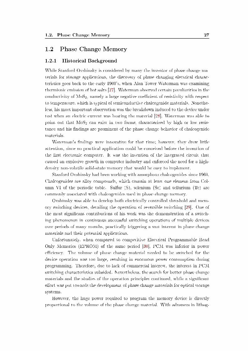
1.2. Phase Change Memory 27
1.2 Phase Change Memory
1.2.1 Historical Background
While Stanford Ovshinsky is considered by many the inventor of phase change ma-
terials for storage applications, the discovery of phase changing electrical charac-
teristics goes back to the early 1900's, when Alan Tower Waterman was examining
thermionic emission of hot salts [27]. Waterman observed certain peculiarities in the
conductivity of MoS2, namely a large negative coecient of resistivity with respect
to temperature, which is typical of semiconductive chalcogenide materials. Nonethe-
less, his most important observation was the breakdown induced to the device under
test when an electric current was heating the material [28]. Waterman was able to
point out that MoS2 can exist in two forms, characterized by high or low resis-
tance and his ndings are prominent of the phase change behavior of chalcogenide
materials.
Waterman's ndings were innovative for that time; however, they drew little
attention, since no practical application could be conceived before the invention of
the rst electronic computer. It was the invention of the integrated circuit that
caused an explosive growth in computer industry and enforced the need for a high-
density non-volatile solid-state memory that would be easy to implement.
Stanford Ovshinsky had been working with amorphous chalcogenides since 1960.
Chalcogenides are alloy compounds, which contain at least one element from Col-
umn VI of the periodic table. Sulfur (S), selenium (Se) and tellurium (Te) are
commonly associated with chalcogenides used in phase change memory.
Ovshinsky was able to develop both electrically controlled threshold and mem-
ory switching devices, detailing the operation of reversible switching [29]. One of
the most signicant contributions of his work was the demonstration of a switch-
ing phenomenon in continuous successful switching operations of multiple devices
over periods of many months, practically triggering a vast interest in phase change
materials and their potential applications.
Unfortunately, when compared to competitive Electrical Programmable Read
Only Memories (EPROM) of the same period [30], PCM was inferior in power
eciency. The volume of phase change material needed to be switched for the
device operation was too large, resulting in enormous power consumption during
programming. Therefore, due to lack of commercial interest, the interest in PCM
switching characteristics subsided. Nevertheless, the search for better phase change
materials and the studies of the operation principles continued, while a signicant
eort was put towards the development of phase change materials for optical storage
systems.
However, the huge power required to program the memory device is directly
proportional to the volume of the phase change material. With advances in lithog-
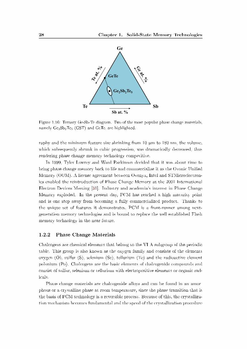
28 Chapter 1. Solid-State Memory Technologies
Ge
Te Sb
GeTe
Ge2Sb2Te5
Sb at. %
Figure 1.16: Ternary Ge-Sb-Te diagram. Two of the most popular phase change materials,
namely Ge2Sb2Te5 (GST) and GeTe, are highlighted.
raphy and the minimum feature size shrinking from 10 µm to 180 nm, the volume,
which subsequently shrunk in cubic progression, was dramatically decreased, thus
rendering phase change memory technology competitive.
In 1999, Tyler Lowrey and Ward Parkinson decided that it was about time to
bring phase change memory back to life and commercialize it as the Ovonic Unied
Memory (OUM). A license agreement between Ovonyx, Intel and STMicroelectron-
ics enabled the reintroduction of Phase Change Memory at the 2001 International
Electron Devices Meeting [31]. Industry and academia's interest in Phase Change
Memory exploded. In the present day, PCM has reached a high maturity point
and is one step away from becoming a fully commercialized product. Thanks to
the unique set of features it demonstrates, PCM is a front-runner among next-
generation memory technologies and is bound to replace the well-established Flash
memory technology in the near future.
1.2.2 Phase Change Materials
Chalcogens are chemical elements that belong to the VI-A subgroup of the periodic
table. This group is also known as the oxygen family and consists of the elements
oxygen (O), sulfur (S), selenium (Se), tellurium (Te) and the radioactive element
polonium (Po). Chalcogens are the basic elements of chalcogenide compounds and
consist of sulfur, selenium or tellurium with electropositive elements or organic rad-
icals.
Phase change materials are chalcogenide alloys and can be found in an amor-
phous or a crystalline phase at room temperature, since the phase transition that is
the basis of PCM technology is a reversible process. Because of this, the crystalliza-
tion mechanism becomes fundamental and the speed of the crystallization procedure
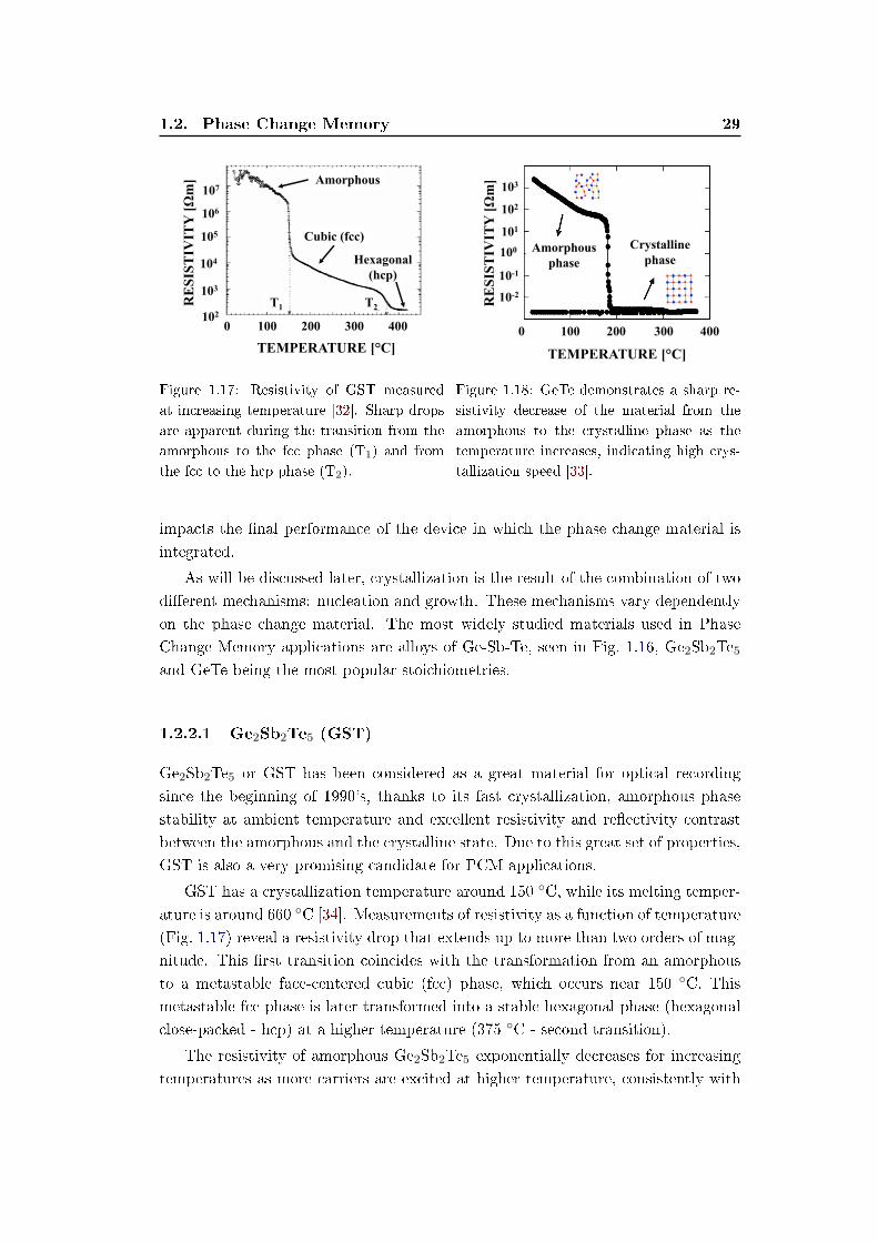
1.2. Phase Change Memory 29
TEMPERATURE [°C]0 100 200 300 400
RE
SIST
IVIT
Y [Ω
m]
106
107
102
105
104
103
T1 T2
Amorphous
Cubic (fcc)
Hexagonal(hcp)
Figure 1.17: Resistivity of GST measured
at increasing temperature [32]. Sharp drops
are apparent during the transition from the
amorphous to the fcc phase (T1) and from
the fcc to the hcp phase (T2).
TEMPERATURE [°C]
RE
SIST
IVIT
Y [Ω
m]
101
102
103
100
10-1
10-2
0 100 200 300 400
Amorphous phase
Crystalline phase
Figure 1.18: GeTe demonstrates a sharp re-
sistivity decrease of the material from the
amorphous to the crystalline phase as the
temperature increases, indicating high crys-
tallization speed [33].
impacts the nal performance of the device in which the phase change material is
integrated.
As will be discussed later, crystallization is the result of the combination of two
dierent mechanisms: nucleation and growth. These mechanisms vary dependently
on the phase change material. The most widely studied materials used in Phase
Change Memory applications are alloys of Ge-Sb-Te, seen in Fig. 1.16, Ge2Sb2Te5and GeTe being the most popular stoichiometries.
1.2.2.1 Ge2Sb2Te5 (GST)
Ge2Sb2Te5 or GST has been considered as a great material for optical recording
since the beginning of 1990's, thanks to its fast crystallization, amorphous phase
stability at ambient temperature and excellent resistivity and reectivity contrast
between the amorphous and the crystalline state. Due to this great set of properties,
GST is also a very promising candidate for PCM applications.
GST has a crystallization temperature around 150 C, while its melting temper-
ature is around 660 C [34]. Measurements of resistivity as a function of temperature
(Fig. 1.17) reveal a resistivity drop that extends up to more than two orders of mag-
nitude. This rst transition coincides with the transformation from an amorphous
to a metastable face-centered cubic (fcc) phase, which occurs near 150 C. This
metastable fcc phase is later transformed into a stable hexagonal phase (hexagonal
close-packed - hcp) at a higher temperature (375 C - second transition).
The resistivity of amorphous Ge2Sb2Te5 exponentially decreases for increasing
temperatures as more carriers are excited at higher temperature, consistently with
30 Chapter 1. Solid-State Memory Technologies
the semiconductive nature of the material [32]. When the material is cooled down,
the resistivity returns to its original value.
However, the resistivity decrease of a crystalline phase at high temperatures is
mainly due to the increase of mobility rather than the increase of carrier concen-
tration. Crystal grains grow during heating and the scattering by grain boundaries
decreases, thus increasing carrier mobility. This decrease in resistivity is irreversible
and the lower resistance persists once the sample is cooled back at room tempera-
ture. The thermal conductivity of GST increases abruptly at 150 C (amorphous to
fcc transition), while it increases more gradually near 340 C (fcc to hcp transition).
Studies on the recrystallization mechanism of amorphous marks upon laser irra-
diation revealed that Ge2Sb2Te5 recrystallizes by nucleation and subsequent growth
of crystals inside the amorphous mark, indicating that the fundamental control
mechanism of crystallization is heterogeneous crystal nucleation [34].
1.2.2.2 GeTe
GeTe is one of the rst examples of chalcogen compounds that demonstrated a
reproducible and controllable phase transition from a low resistive, low reective
crystalline state, to a low resistive, low reective amorphous state.
At room temperature, the crystalline phase forms in rhombohedral structure.
The GeTe lattice can be visualized as a distorted rocksalt structure with Ge and
Te uniquely located on fcc structures that undergo a distortion along the [1 1 1]
direction [35]. Upon heating above 400 C, GeTe transforms into a higher-symmetry
cubic phase with a small volume reduction (on the order of 1%).
GeTe is a degenerated p-type semiconductor with the top of the valence band
formed by p-type electrons. In the near-perfect cubic phase, all atoms and con-
sequently their p orbitals are aligned and the resonant-bonding network extends
throughout the crystal, while in the amorphous phase, resonance bonding is local-
ized to within fewer interatomic distances. Consequently, the two phases have very
dierent electrical and thermal conductivity [36].
GeTe is still largely investigated because of its high crystallization speed [37].
Most of the pre-amorphized surface tends to recrystallize starting from the interface
between the amorphous region and the surrounding crystalline phase. In really long
crystallization procedures, nucleation coupled with growth can be observed [38].
The crystallization temperature of GeTe is around 180 C, while its melting
temperature is around 725 C [39]. The transition from the amorphous to the
crystalline phase is quite abrupt, indicating the rapid growth of a generated crystal
that leads to instantaneous crystallization. This phenomenon is evident as an abrupt
transition in optical and resistivity measurements (Fig. 1.18), highlighting the high
crystallization speed of the material.
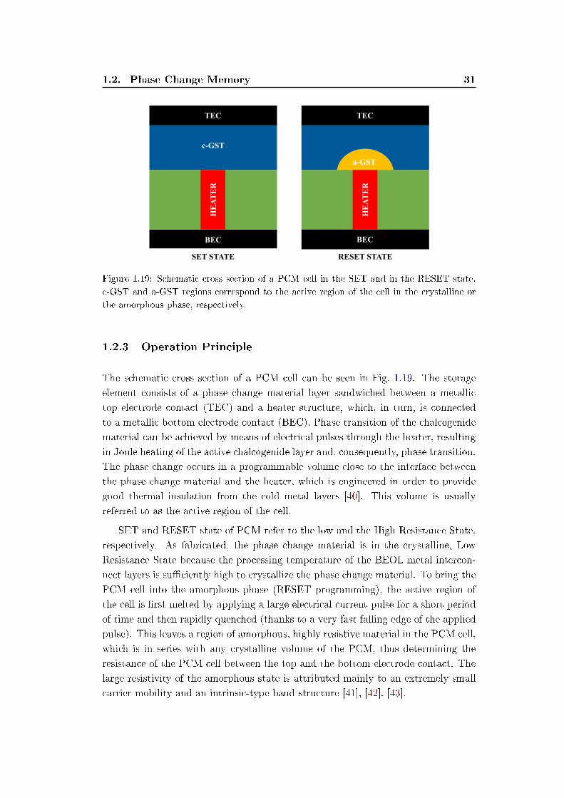
1.2. Phase Change Memory 31
TEC
HE
AT
ER
SET STATE
BEC
c-GST
TEC
RESET STATE
BEC
HE
AT
ER
a-GST
Figure 1.19: Schematic cross section of a PCM cell in the SET and in the RESET state.
c-GST and a-GST regions correspond to the active region of the cell in the crystalline or
the amorphous phase, respectively.
1.2.3 Operation Principle
The schematic cross section of a PCM cell can be seen in Fig. 1.19. The storage
element consists of a phase change material layer sandwiched between a metallic
top electrode contact (TEC) and a heater structure, which, in turn, is connected
to a metallic bottom electrode contact (BEC). Phase transition of the chalcogenide
material can be achieved by means of electrical pulses through the heater, resulting
in Joule heating of the active chalcogenide layer and, consequently, phase transition.
The phase change occurs in a programmable volume close to the interface between
the phase change material and the heater, which is engineered in order to provide
good thermal insulation from the cold metal layers [40]. This volume is usually
referred to as the active region of the cell.
SET and RESET state of PCM refer to the low and the High Resistance State,
respectively. As fabricated, the phase change material is in the crystalline, Low
Resistance State because the processing temperature of the BEOL metal intercon-
nect layers is suciently high to crystallize the phase change material. To bring the
PCM cell into the amorphous phase (RESET programming), the active region of
the cell is rst melted by applying a large electrical current pulse for a short period
of time and then rapidly quenched (thanks to a very fast falling edge of the applied
pulse). This leaves a region of amorphous, highly resistive material in the PCM cell,
which is in series with any crystalline volume of the PCM, thus determining the
resistance of the PCM cell between the top and the bottom electrode contact. The
large resistivity of the amorphous state is attributed mainly to an extremely small
carrier mobility and an intrinsic-type band structure [41], [42], [43].
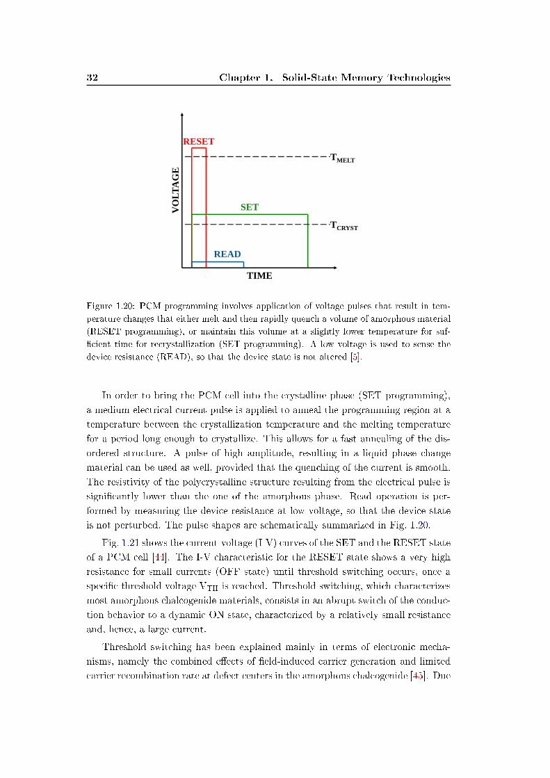
32 Chapter 1. Solid-State Memory Technologies
READ
SET
RESET
TMELT
TCRYST
VO
LTA
GE
TIME
Figure 1.20: PCM programming involves application of voltage pulses that result in tem-
perature changes that either melt and then rapidly quench a volume of amorphous material
(RESET programming), or maintain this volume at a slightly lower temperature for suf-
cient time for recrystallization (SET programming). A low voltage is used to sense the
device resistance (READ), so that the device state is not altered [5].
In order to bring the PCM cell into the crystalline phase (SET programming),
a medium electrical current pulse is applied to anneal the programming region at a
temperature between the crystallization temperature and the melting temperature
for a period long enough to crystallize. This allows for a fast annealing of the dis-
ordered structure. A pulse of high amplitude, resulting in a liquid phase change
material can be used as well, provided that the quenching of the current is smooth.
The resistivity of the polycrystalline structure resulting from the electrical pulse is
signicantly lower than the one of the amorphous phase. Read operation is per-
formed by measuring the device resistance at low voltage, so that the device state
is not perturbed. The pulse shapes are schematically summarized in Fig. 1.20.
Fig. 1.21 shows the current-voltage (I-V) curves of the SET and the RESET state
of a PCM cell [44]. The I-V characteristic for the RESET state shows a very high
resistance for small currents (OFF state) until threshold switching occurs, once a
specic threshold voltage VTH is reached. Threshold switching, which characterizes
most amorphous chalcogenide materials, consists in an abrupt switch of the conduc-
tion behavior to a dynamic ON state, characterized by a relatively small resistance
and, hence, a large current.
Threshold switching has been explained mainly in terms of electronic mecha-
nisms, namely the combined eects of eld-induced carrier generation and limited
carrier recombination rate at defect centers in the amorphous chalcogenide [45]. Due
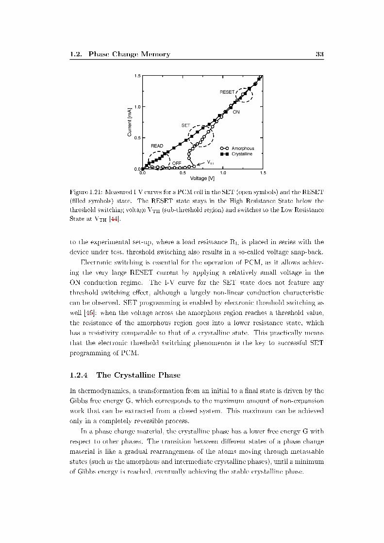
1.2. Phase Change Memory 33
Figure 1.21: Measured I-V curves for a PCM cell in the SET (open symbols) and the RESET
(lled symbols) state. The RESET state stays in the High Resistance State below the
threshold switching voltage VTH (sub-threshold region) and switches to the Low Resistance
State at VTH [44].
to the experimental set-up, where a load resistance RL is placed in series with the
device under test, threshold switching also results in a so-called voltage snap-back.
Electronic switching is essential for the operation of PCM, as it allows achiev-
ing the very large RESET current by applying a relatively small voltage in the
ON conduction regime. The I-V curve for the SET state does not feature any
threshold switching eect, although a largely non-linear conduction characteristic
can be observed. SET programming is enabled by electronic threshold switching as
well [46]: when the voltage across the amorphous region reaches a threshold value,
the resistance of the amorphous region goes into a lower resistance state, which
has a resistivity comparable to that of a crystalline state. This practically means
that the electronic threshold switching phenomenon is the key to successful SET
programming of PCM.
1.2.4 The Crystalline Phase
In thermodynamics, a transformation from an initial to a nal state is driven by the
Gibbs free energy G, which corresponds to the maximum amount of non-expansion
work that can be extracted from a closed system. This maximum can be achieved
only in a completely reversible process.
In a phase change material, the crystalline phase has a lower free energy G with
respect to other phases. The transition between dierent states of a phase change
material is like a gradual rearrangement of the atoms moving through metastable
states (such as the amorphous and intermediate crystalline phases), until a minimum
of Gibbs energy is reached, eventually achieving the stable crystalline phase.
34 Chapter 1. Solid-State Memory Technologies
This atomic rearrangement occurs when a given activation energy barrier is
overcome. Temperature plays a key role in this mechanism, since an increase of the
material temperature can boost the crystallization process, giving rise to a number
of metastable phases that depend on the elemental composition of the phase change
material.
Ge2Sb2Te5, which is the most commonly used phase change material, demon-
strates a hexagonal stable crystal structure (hcp structure) but, depending on the
recrystallization procedure, a metastable rocksalt structure (fcc structure) can be
observed, with Te atoms occupying sites on one fcc sub-lattice and Ge and Sb ran-
domly forming another fcc sub-lattice (20% of the sites being vacant) [47].
Crystallization of GST in the cubic structure (which is rather isotropic and
hence more similar to the amorphous structure than any other crystal structure) is
the reason for the high-speed switching and reproducible performance, since the hcp
structure is more energetically expensive to obtain. The presence of vacancies in
the lattice means that covalent bond lengths are slightly dierent from each other
and that the lattice is distorted. Moreover, there is a low volume dierence between
the amorphous and the fcc-type crystalline phase, possibly due to the presence of
vacancies. Finally, the basis of the fcc structure of the Ge2Sb2Te5 metastable state
seems to be some slight changes in the covalent bonding angle, facilitated at high
temperature [48].
1.2.4.1 Crystallization Kinetics
The crystallization mechanism impacts many aspects of the performance of a PCM
device, aecting the programming speed and the stability of the amorphous phase.
In order to describe the crystallization process, the Classical Nucleation Theory
developed by Gibbs in 1878 may be used. According to that theory, the composition
of the material during crystallization remains unchanged and the entire process
demonstrates a diusion-limited nature.
A cluster of crystalline phase growing in the surrounding amorphous phase is
expressed as the sum of the bulk contributions of the nucleus and the amorphous
phase. Applying the Classical Nucleation Theory to cluster formation, an increase
of the characteristic thermodynamic potential is observed and a subsequent creation
of a critical cluster size (crystal nucleation). Only clusters with sizes larger than
the critical size are capable of growing in a deterministic way to macroscopic sizes
(crystal growth). The change of the characteristic thermodynamic potential result-
ing from the formation of a cluster of critical size is commonly denoted as the work of
critical cluster formation. This quantity reects the thermodynamic (or energetic)
aspect of nucleation.
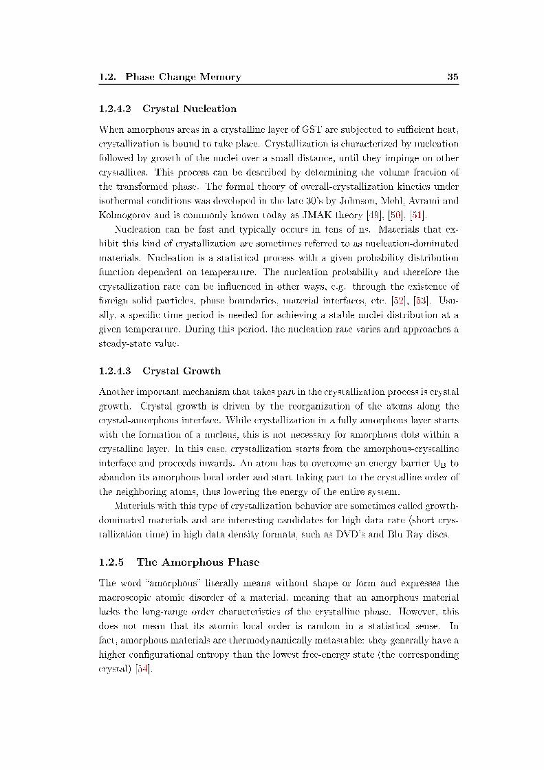
1.2. Phase Change Memory 35
1.2.4.2 Crystal Nucleation
When amorphous areas in a crystalline layer of GST are subjected to sucient heat,
crystallization is bound to take place. Crystallization is characterized by nucleation
followed by growth of the nuclei over a small distance, until they impinge on other
crystallites. This process can be described by determining the volume fraction of
the transformed phase. The formal theory of overall-crystallization kinetics under
isothermal conditions was developed in the late 30's by Johnson, Mehl, Avrami and
Kolmogorov and is commonly known today as JMAK theory [49], [50], [51].
Nucleation can be fast and typically occurs in tens of ns. Materials that ex-
hibit this kind of crystallization are sometimes referred to as nucleation-dominated
materials. Nucleation is a statistical process with a given probability distribution
function dependent on temperature. The nucleation probability and therefore the
crystallization rate can be inuenced in other ways, e.g. through the existence of
foreign solid particles, phase boundaries, material interfaces, etc. [52], [53]. Usu-
ally, a specic time period is needed for achieving a stable nuclei distribution at a
given temperature. During this period, the nucleation rate varies and approaches a
steady-state value.
1.2.4.3 Crystal Growth
Another important mechanism that takes part in the crystallization process is crystal
growth. Crystal growth is driven by the reorganization of the atoms along the
crystal-amorphous interface. While crystallization in a fully amorphous layer starts
with the formation of a nucleus, this is not necessary for amorphous dots within a
crystalline layer. In this case, crystallization starts from the amorphous-crystalline
interface and proceeds inwards. An atom has to overcome an energy barrier UB to
abandon its amorphous local order and start taking part to the crystalline order of
the neighboring atoms, thus lowering the energy of the entire system.
Materials with this type of crystallization behavior are sometimes called growth-
dominated materials and are interesting candidates for high data rate (short crys-
tallization time) in high data density formats, such as DVD's and Blu-Ray discs.
1.2.5 The Amorphous Phase
The word amorphous literally means without shape or form and expresses the
macroscopic atomic disorder of a material, meaning that an amorphous material
lacks the long-range order characteristics of the crystalline phase. However, this
does not mean that its atomic local order is random in a statistical sense. In
fact, amorphous materials are thermodynamically metastable: they generally have a
higher congurational entropy than the lowest free-energy state (the corresponding
crystal) [54].
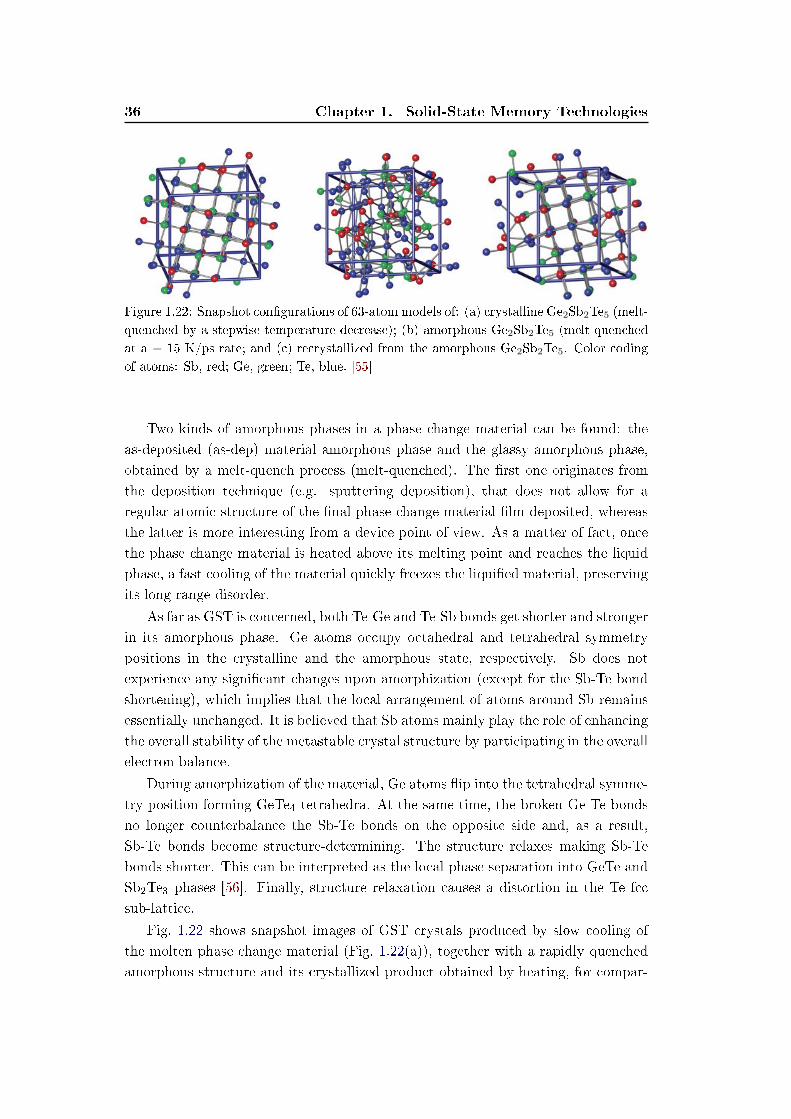
36 Chapter 1. Solid-State Memory Technologies
Figure 1.22: Snapshot congurations of 63-atom models of: (a) crystalline Ge2Sb2Te5 (melt-
quenched by a stepwise temperature decrease); (b) amorphous Ge2Sb2Te5 (melt-quenched
at a − 15 K/ps rate; and (c) recrystallized from the amorphous Ge2Sb2Te5. Color coding
of atoms: Sb, red; Ge, green; Te, blue. [55]
Two kinds of amorphous phases in a phase change material can be found: the
as-deposited (as-dep) material amorphous phase and the glassy amorphous phase,
obtained by a melt-quench process (melt-quenched). The rst one originates from
the deposition technique (e.g. sputtering deposition), that does not allow for a
regular atomic structure of the nal phase change material lm deposited, whereas
the latter is more interesting from a device point of view. As a matter of fact, once
the phase change material is heated above its melting point and reaches the liquid
phase, a fast cooling of the material quickly freezes the liquied material, preserving
its long range disorder.
As far as GST is concerned, both Te-Ge and Te-Sb bonds get shorter and stronger
in its amorphous phase. Ge atoms occupy octahedral and tetrahedral symmetry
positions in the crystalline and the amorphous state, respectively. Sb does not
experience any signicant changes upon amorphization (except for the Sb-Te bond
shortening), which implies that the local arrangement of atoms around Sb remains
essentially unchanged. It is believed that Sb atoms mainly play the role of enhancing
the overall stability of the metastable crystal structure by participating in the overall
electron balance.
During amorphization of the material, Ge atoms ip into the tetrahedral symme-
try position forming GeTe4 tetrahedra. At the same time, the broken Ge-Te bonds
no longer counterbalance the Sb-Te bonds on the opposite side and, as a result,
Sb-Te bonds become structure-determining. The structure relaxes making Sb-Te
bonds shorter. This can be interpreted as the local phase separation into GeTe and
Sb2Te3 phases [56]. Finally, structure relaxation causes a distortion in the Te fcc
sub-lattice.
Fig. 1.22 shows snapshot images of GST crystals produced by slow cooling of
the molten phase change material (Fig. 1.22(a)), together with a rapidly quenched
amorphous structure and its crystallized product obtained by heating, for compar-
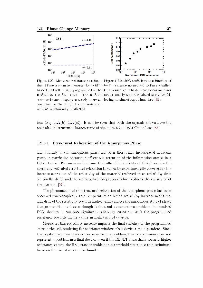
1.2. Phase Change Memory 37
102 104 106
104
105
106
107
103
RE
SIST
AN
CE
[Ω]
TIME [s]108100
GST108
ν = 0.11
ν < 0.01
Figure 1.23: Measured resistance as a func-
tion of time at room temperature for a GST-
based PCM cell initially programmed in the
RESET or the SET state. The RESET
state resistance displays a steady increase
over time, while the SET state resistance
remains substantially unaected.
Figure 1.24: Drift coecient as a function of
GST resistance normalized to the crystalline
GST resistance. The drift coecient increases
monotonically with normalized resistance fol-
lowing an almost logarithmic law [58].
ison (Fig. 1.22(b), 1.22(c)). It can be seen that both the crystals shown have the
rocksalt-like structure characteristic of the metastable crystalline phase [55].
1.2.5.1 Structural Relaxation of the Amorphous Phase
The stability of the amorphous phase has been thoroughly investigated in recent
years, in particular because it aects the retention of the information stored in a
PCM device. The main mechanisms that aect the stability of this phase are the
thermally activated structural relaxation that can be experimentally observed as the
increase over time of the resistivity of the material (referred to as resistivity drift
or, briey, drift) and the recrystallization process, which reduces the resistivity of
the material [57].
The phenomenon of the structural relaxation of the amorphous phase has been
observed macroscopically as a temperature-activated resistivity increase over time.
The drift of the resistivity towards higher values aects the amorphous state of phase
change materials and even though it does not cause serious problems in standard
PCM devices, it can pose signicant reliability issues and shift the programmed
resistance towards higher values in highly scaled devices.
Moreover, this resistivity increase impacts the nal stability of the programmed
state in the cell, rendering the resistance window of the device time-dependent. Since
the crystalline phase does not experience this problem, this phenomenon does not
represent a problem in a nal device: even if the RESET state drifts towards higher
resistance values, the SET state is stable and a threshold resistance to discriminate
between the two states can be found.
38 Chapter 1. Solid-State Memory Technologies
The physics involved in the drift behavior is still debated and the phenomenon
can be observed in as-dep [59] [60] and in melt-quenched phase change materials,
meaning that probably all the mechanisms proposed have a contribution in the drift
of the amorphous state. In all theoretical models proposed so far [61], resistivity
drift is phenomenologically represented by a power law equation:
ρ = ρ0(tt0)ν (1.1)
where ρ is the electrical resistivity, t0 is an arbitrary time set at the end of the
recovery time for the amorphous material and ρ0 is the value of resistivity at t0.
The exponent ν is known as the drift coecient [62].
Starting from this equation and considering that it has been experimentally
demonstrated that the observed drift coecient ν increases as the resistance of the
cell increases [57], the resistance evolution over time is given by
R = R0(tt0)ν (1.2)
In this case, the drift coecient ν represents the slope of the resistance vs. time curve
in log-log scale for the amorphous (ν = 0.11) and the crystalline phase (ν < 0.01)
of GST [63], as shown in Fig. 1.23.
The fact that the resistance coecient depends on the programmed resistance
state (Fig. 1.24) may become detrimental in Multilevel Cell applications, where the
cell is also programmed to intermediate resistance states. This potential reliability
issue calls for novel programming and reading techniques at system level, to ensure
storage reliability [64], [65]. At the same time, experimental results also show that
due to its stochastic nature, the drift phenomenon broadens the resistance dispersion
of the devices when the resistance value increases [66].
After the application of a RESET pulse, the threshold voltage that is required
in order to switch the amorphized volume of the phase change material exhibits an
increase over time as well. The evolution in time of the threshold voltage is also
correlated to the structural relaxation of the amorphous material. This phenomenon
is referred to as threshold recovery or drift of the threshold voltage.
The equation that describes the drift of the threshold voltage over time is:
VTH = VTH,0[1+ βln(tτ0
)] (1.3)
where VTH,0 is the value of the threshold voltage at the characteristic time τ0 (con-
sidered as the delay time for the activation of the drift phenomenon) and β is referred
to as the drift parameter.
If the trap decay model is used to explain the threshold voltage drift phe-
nomenon [63], then VTH can be tted with a power law similar to the one seen
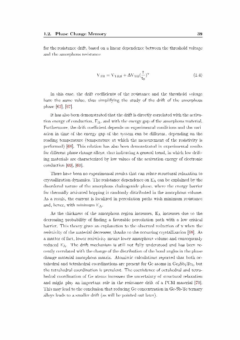
1.2. Phase Change Memory 39
for the resistance drift, based on a linear dependence between the threshold voltage
and the amorphous resistance
VTH = VTH,0 + ∆VTH(tt0)ν (1.4)
In this case, the drift coecients of the resistance and the threshold voltage
have the same value, thus simplifying the study of the drift of the amorphous
phase [62], [67].
It has also been demonstrated that the drift is directly correlated with the activa-
tion energy of conduction, EA, and with the energy gap of the amorphous material.
Furthermore, the drift coecient depends on experimental conditions and the vari-
ation in time of the energy gap of the system can be dierent, depending on the
reading temperature (temperature at which the measurement of the resistivity is
performed) [68]. This relation has also been demonstrated in experimental results
for dierent phase change alloys, thus indicating a general trend, in which low drift-
ing materials are characterized by low values of the activation energy of electronic
conduction [69], [60].
There have been no experimental results that can relate structural relaxation to
crystallization dynamics. The resistance dependence on EA can be explained by the
disordered nature of the amorphous chalcogenide phase, where the energy barrier
for thermally activated hopping is randomly distributed in the amorphous volume.
As a result, the current is localized in percolation paths with minimum resistance
and, hence, with minimum EA.
As the thickness of the amorphous region increases, EA increases due to the
decreasing probability of nding a favorable percolation path with a low critical
barrier. This theory gives an explanation to the observed reduction of ν when the
resistivity of the material decreases, thanks to the occurring crystallization [68]. As
a matter of fact, lower resistivity means lower amorphous volume and consequently
reduced EA. The drift mechanism is still not fully understood and has been re-
cently correlated with the change of the distribution of the bond angles in the phase
change material amorphous matrix. Atomistic calculations reported that both oc-
tahedral and tetrahedral coordinations are present for Ge atoms in Ge2Sb2Te5, but
the tetrahedral coordination is prevalent. The coexistence of octahedral and tetra-
hedral coordination of Ge atoms increases the uncertainty of structural relaxation
and might play an important role in the resistance drift of a PCM material [70].
This may lead to the conclusion that reducing Ge concentration in Ge-Sb-Te ternary
alloys leads to a smaller drift (as will be pointed out later).
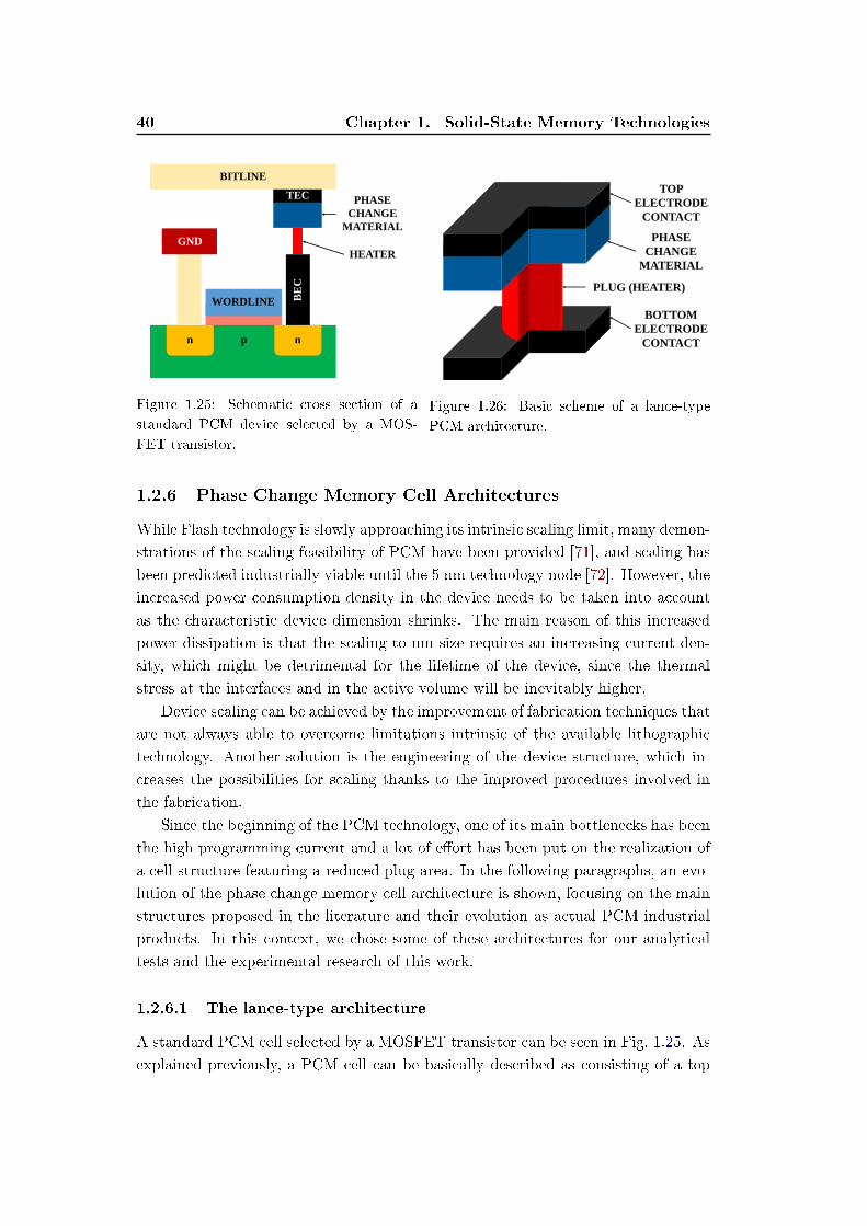
40 Chapter 1. Solid-State Memory Technologies
WORDLINE
n np
GND
BITLINE
TEC
BE
C
PHASE CHANGE
MATERIAL
HEATER
Figure 1.25: Schematic cross section of a
standard PCM device selected by a MOS-
FET transistor.
PHASE CHANGE
MATERIAL
PLUG (HEATER)
TOP ELECTRODE
CONTACT
BOTTOM ELECTRODE
CONTACT
Figure 1.26: Basic scheme of a lance-type
PCM architecture.
1.2.6 Phase Change Memory Cell Architectures
While Flash technology is slowly approaching its intrinsic scaling limit, many demon-
strations of the scaling feasibility of PCM have been provided [71], and scaling has
been predicted industrially viable until the 5 nm technology node [72]. However, the
increased power consumption density in the device needs to be taken into account
as the characteristic device dimension shrinks. The main reason of this increased
power dissipation is that the scaling to nm size requires an increasing current den-
sity, which might be detrimental for the lifetime of the device, since the thermal
stress at the interfaces and in the active volume will be inevitably higher.
Device scaling can be achieved by the improvement of fabrication techniques that
are not always able to overcome limitations intrinsic of the available lithographic
technology. Another solution is the engineering of the device structure, which in-
creases the possibilities for scaling thanks to the improved procedures involved in
the fabrication.
Since the beginning of the PCM technology, one of its main bottlenecks has been
the high programming current and a lot of eort has been put on the realization of
a cell structure featuring a reduced plug area. In the following paragraphs, an evo-
lution of the phase change memory cell architecture is shown, focusing on the main
structures proposed in the literature and their evolution as actual PCM industrial
products. In this context, we chose some of these architectures for our analytical
tests and the experimental research of this work.
1.2.6.1 The lance-type architecture
A standard PCM cell selected by a MOSFET transistor can be seen in Fig. 1.25. As
explained previously, a PCM cell can be basically described as consisting of a top
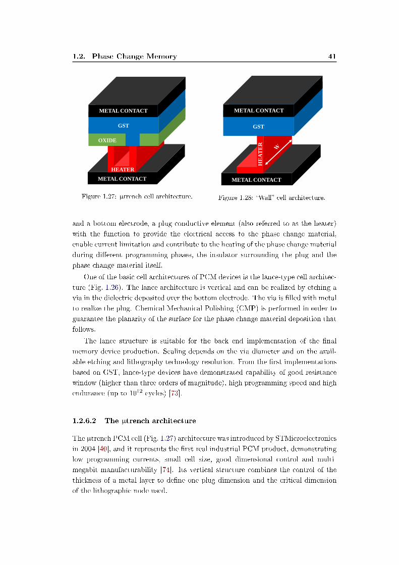
1.2. Phase Change Memory 41
METAL CONTACT
GST
HE
AT
ER
GST
OXIDE
HEATER
METAL CONTACT
METAL CONTACT
Figure 1.27: µtrench cell architecture.
METAL CONTACT
METAL CONTACT
GST
HE
AT
ER
METAL CONTACT
Figure 1.28: Wall cell architecture.
and a bottom electrode, a plug conductive element (also referred to as the heater)
with the function to provide the electrical access to the phase change material,
enable current limitation and contribute to the heating of the phase change material
during dierent programming phases, the insulator surrounding the plug and the
phase change material itself.
One of the basic cell architectures of PCM devices is the lance-type cell architec-
ture (Fig. 1.26). The lance architecture is vertical and can be realized by etching a
via in the dielectric deposited over the bottom electrode. The via is lled with metal
to realize the plug. Chemical Mechanical Polishing (CMP) is performed in order to
guarantee the planarity of the surface for the phase change material deposition that
follows.
The lance structure is suitable for the back end implementation of the nal
memory device production. Scaling depends on the via diameter and on the avail-
able etching and lithography technology resolution. From the rst implementations
based on GST, lance-type devices have demonstrated capability of good resistance
window (higher than three orders of magnitude), high programming speed and high
endurance (up to 1012 cycles) [73].
1.2.6.2 The µtrench architecture
The µtrench PCM cell (Fig. 1.27) architecture was introduced by STMicroelectronics
in 2004 [40], and it represents the rst real industrial PCM product, demonstrating
low programming currents, small cell size, good dimensional control and multi-
megabit manufacturability [74]. Its vertical structure combines the control of the
thickness of a metal layer to dene one plug dimension and the critical dimension
of the lithographic node used.
42 Chapter 1. Solid-State Memory Technologies
This structure has also been implemented in order to study the eects of scaling
and the reliability of this technology. In this structure, the interface area is dened
by the ring thickness and the trench width. The main resistive contribution of the
plug to the programming of the cell (RON) is in the regions close to the plug/phase
change material interface. As a matter of fact, moving from the interface towards the
inside of the ring, the current density rapidly decreases due to the larger eective area
of the ring. This poses problems for the engineering of the plug, since an appropriate
RON to allow SET and RESET operations without the need of an external selector
device to limit the current is dicult to achieve.
Nevertheless, a great advantage of the µtrench architecture is fast programming,
thanks to the fact that the peak of the current density is always at the plug/phase
change material interface and the reduction of the power dissipated in the plug.
However, co-integration with an MOS selector becomes necessary.
1.2.6.3 The Wall architecture
The Wall structure (Fig. 1.28) represents the direct evolution of the µtrench ar-
chitecture. When compared to the µtrench cell, the Wall structure has better
lithographic alignment tolerances while still preserving good programming current
control and allows saving one critical mask, thus simplifying the storage element
process integration [75]. A thin-lm vertical heater element is dened on top of a
tungsten contact and a GST layer is directly deposited and self-aligned etched to
form the BL. From a functional point of view, this structure enables better engi-
neering of the cell with respect to programming operations [76].
The analysis of the structure eciency shows that the increase of the heater
resistance (for better current control) produces a displacement of the temperature
peak inside the plug, with a consequent reduction of the power eciency of the de-
vice [77]. The scaling of cell has to be coupled to a proper selection of the properties
(thermal and electrical) of the integrated phase change material. As we will present
in the following sections, the reliability studies of this work were performed on state-
of-the-art Wall PCM devices fabricated in collaboration with STMicroelectronics.
1.2.6.4 The conned architecture
As already pointed out, scaling of vertical structures is limited by the increase of
the current density required to program the cell due to the increased contribution of
the lateral thermal dissipation of the structure at lower dimensions. The idea of the
conned structure is to conne the phase change material in the same hole realized
to implement the plug element, partially or totally replacing it. This enhances the
thermal connement of the active volume, since the power delivered to the phase
change material is conned by the dielectric.
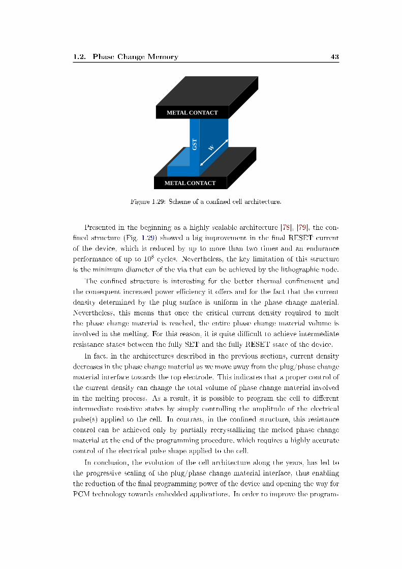
1.2. Phase Change Memory 43
METAL CONTACT
METAL CONTACT
GST
Figure 1.29: Scheme of a conned cell architecture.
Presented in the beginning as a highly scalable architecture [78], [79], the con-
ned structure (Fig. 1.29) showed a big improvement in the nal RESET current
of the device, which is reduced by up to more than two times and an endurance
performance of up to 108 cycles. Nevertheless, the key limitation of this structure
is the minimum diameter of the via that can be achieved by the lithographic node.
The conned structure is interesting for the better thermal connement and
the consequent increased power eciency it oers and for the fact that the current
density determined by the plug surface is uniform in the phase change material.
Nevertheless, this means that once the critical current density required to melt
the phase change material is reached, the entire phase change material volume is
involved in the melting. For this reason, it is quite dicult to achieve intermediate
resistance states between the fully SET and the fully RESET state of the device.
In fact, in the architectures described in the previous sections, current density
decreases in the phase change material as we move away from the plug/phase change
material interface towards the top electrode. This indicates that a proper control of
the current density can change the total volume of phase change material involved
in the melting process. As a result, it is possible to program the cell to dierent
intermediate resistive states by simply controlling the amplitude of the electrical
pulse(s) applied to the cell. In contrast, in the conned structure, this resistance
control can be achieved only by partially recrystallizing the melted phase change
material at the end of the programming procedure, which requires a highly accurate
control of the electrical pulse shape applied to the cell.
In conclusion, the evolution of the cell architecture along the years, has led to
the progressive scaling of the plug/phase change material interface, thus enabling
the reduction of the nal programming power of the device and opening the way for
PCM technology towards embedded applications. In order to improve the program-
44 Chapter 1. Solid-State Memory Technologies
ming speed of the device, the current density increase provided at the plug/phase
change material interface in the µtrench structure represents a great solution, also
in terms of programming power reduction. However, the absence of a real intrinsic
current limitation requires external current control that should be provided by an
access transistor, which makes the µtrench architecture not suitable for crossbar
applications. In terms of thermal connement of the phase change material and
consequent reduction of programming current density, the conned structure repre-
sents the best solution. However, this structure requires highly conformal deposition
techniques. The best compromise in terms of fabrication process, scaling capability
and device engineering opportunity, is the Wall structure that represents nowadays
the state-of-the-art of industrial PCM products.
1.2.7 PCM Applications and Challenges
Phase Change Memory has made rapid progress in a short time, having left behind
older technologies in terms of both sophisticated demonstrations of scaling to small
device dimensions, as well as integrated large-array demonstrators with impressive
data retention, endurance, performance and yield characteristics. PCM supports
the promise of scalability beyond that of other memory technologies, with proven
scalability down to the 5 nm node [72].
The range of applications in which PCM technology can be used is quite exten-
sive, including [80]:
i. ultra high-performance memory subsystems to achieve solid-state drive (SSD)
performance and reliability that is unachievable with Flash NAND and at power
consumption levels that cannot be achieved with conventional SRAM technol-
ogy;
ii. execution memory in embedded systems, thanks to its single bit-alterability;
iii. wireless systems for data storage and/or direct software execution (read latency
comparable to DRAM);
iv. computing platforms where the non-volatility of stored data allows for energy
saving.
In order to become competitive in these markets, PCM needs to match the
cost of existing technologies in terms of cell size and process complexity, providing
good perspectives in future scalability and nding application opportunities in the
optimization of the overall memory system.
Currently, one of the most critical issues that prevents PCM from accomplishing
large scale adoption in the NVM market is its large programming current. Since the
cell selector must provide this large programming current, it can be concluded that
1.2. Phase Change Memory 45
the selector device area may become the limiting factor in device density. For this
reason, a reduction of the programming current would be benecial not only for the
decrease of the power consumption but also for applications where high density is
necessary. Finally, two additional challenges remain for this technology and prevent
it from becoming a denitive Flash replacement in the near future: data retention
in high temperature environments (such as automotive applications) and multilevel
capability.
A comparison of PCM with established memory technologies (DRAM, SRAM,
Flash) that also highlights its potential for use in embedded and stand-alone appli-
cations follows next. Furthermore, the concept of Storage Class Memory, for which
PCM seems to be an ideal candidate, is introduced. The stringent requirements
for use of PCM in automotive applications are discussed, while the Multilevel Cell
programming capabilities and the factors that aect its reliability are also examined
at the end of the Section.
1.2.7.1 Universal Memory
The extent to which non-volatile memories (NVM) have invaded our everyday lives is
truly remarkable. From music on MP3 players to photos on digital cameras, stored
e-mail and text messages on smartphones, the documents we carry on our USB
drives and the program code that enables everything from our portable electronics
to cars, NVM, mainly Flash memory, is everywhere around us.
New NVM candidate technologies have been under consideration as possible
Flash replacements for more than a decade. For these reasons, PCM is expected
to compare to the major incumbent memory technologies in terms of cost and per-
formance. Table 1.1 summarizes the basic features of existing memory technologies
(SRAM, DRAM, NAND Flash memory) and memory concepts that have emerged
during the past decade, indicating the superior performance of PCM and its poten-
tial to be used in a wide range of possible applications.
As far as the comparison to SRAM is concerned, PCM has proven its ability to
scale down and thus compete with the large SRAM cell size, even though a large
access device may be used for the PCM cell. Nevertheless, SRAM performance
is hard to match. The performance limiter for PCM is the SET programming
speed, which depends on the crystallization speed of the phase change material.
Furthermore, the most stringent requirement for any emerging memory technology
that seeks to replace SRAM is endurance. The read/write endurance of SRAM
is substantially innite. While read endurance does not pose signicant issues for
PCM, the required write endurance should be in the order of 1015 cycles, which is
almost impossible to achieve.
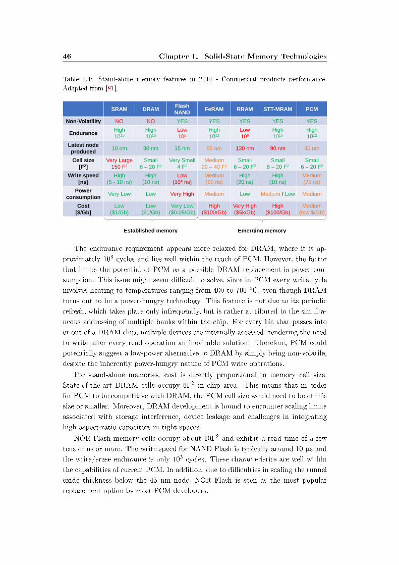
46 Chapter 1. Solid-State Memory Technologies
Table 1.1: Stand-alone memory features in 2014 - Commercial products performance.
Adapted from [81].
SRAM DRAMFlash NAND
FeRAM RRAM STT-MRAM PCM
Non-Volatility NO NO YES YES YES YES YES
EnduranceHigh1015
High1015
Low105
High1012
Low106
High1015
High 1012
Latest node produced
10 nm 30 nm 15 nm 65 nm 130 nm 90 nm 45 nm
Cell size [F2]
Very Large150 F2
Small6 – 20 F2
Very Small4 F2
Medium20 – 40 F2
Small6 – 20 F2
Small6 – 20 F2
Small6 – 20 F2
Write speed [ns]
High (5 - 10 ns)
High (10 ns)
Low (104 ns)
Medium(50 ns)
High (20 ns)
High (10 ns)
Medium (75 ns)
Power consumption
Very Low Low Very High Medium Low Medium / Low Medium
Cost[$/Gb]
Low($1/Gb)
Low($1/Gb)
Very Low($0.05/Gb)
High($100/Gb)
Very High($5k/Gb)
High($100/Gb)
Medium(few $/Gb)
Established memory Emerging memory
The endurance requirement appears more relaxed for DRAM, where it is ap-
proximately 108 cycles and lies well within the reach of PCM. However, the factor
that limits the potential of PCM as a possible DRAM replacement is power con-
sumption. This issue might seem dicult to solve, since in PCM every write cycle
involves heating to temperatures ranging from 400 to 700 C, even though DRAM
turns out to be a power-hungry technology. This feature is not due to its periodic
refresh, which takes place only infrequently, but is rather attributed to the simulta-
neous addressing of multiple banks within the chip. For every bit that passes into
or out of a DRAM chip, multiple devices are internally accessed, rendering the need
to write after every read operation an inevitable solution. Therefore, PCM could
potentially suggest a low-power alternative to DRAM by simply being non-volatile,
despite the inherently power-hungry nature of PCM write operations.
For stand-alone memories, cost is directly proportional to memory cell size.
State-of-the-art DRAM cells occupy 6F2 in chip area. This means that in order
for PCM to be competitive with DRAM, the PCM cell size would need to be of this
size or smaller. Moreover, DRAM development is bound to encounter scaling limits
associated with storage interference, device leakage and challenges in integrating
high aspect-ratio capacitors in tight spaces.
NOR Flash memory cells occupy about 10F2 and exhibit a read time of a few
tens of ns or more. The write speed for NAND Flash is typically around 10 µs and
the write/erase endurance is only 105 cycles. These characteristics are well within
the capabilities of current PCM. In addition, due to diculties in scaling the tunnel
oxide thickness below the 45 nm node, NOR Flash is seen as the most popular
replacement option by most PCM developers.
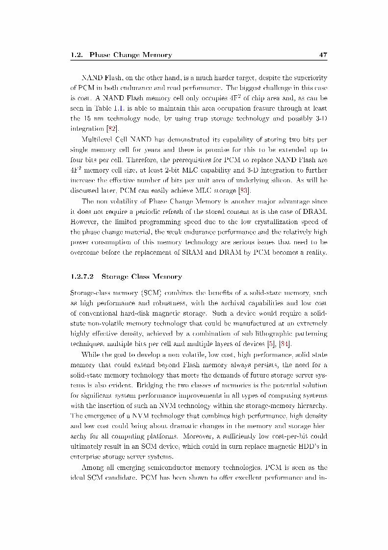
1.2. Phase Change Memory 47
NAND Flash, on the other hand, is a much harder target, despite the superiority
of PCM in both endurance and read performance. The biggest challenge in this case
is cost. A NAND Flash memory cell only occupies 4F2 of chip area and, as can be
seen in Table 1.1, is able to maintain this area occupation feature through at least
the 15 nm technology node, by using trap storage technology and possibly 3-D
integration [82].
Multilevel Cell NAND has demonstrated its capability of storing two bits per
single memory cell for years and there is promise for this to be extended up to
four bits per cell. Therefore, the prerequisites for PCM to replace NAND Flash are
4F2 memory cell size, at least 2-bit MLC capability and 3-D integration to further
increase the eective number of bits per unit area of underlying silicon. As will be
discussed later, PCM can easily achieve MLC storage [83].
The non-volatility of Phase Change Memory is another major advantage since
it does not require a periodic refresh of the stored content as is the case of DRAM.
However, the limited programming speed due to the low crystallization speed of
the phase change material, the weak endurance performance and the relatively high
power consumption of this memory technology are serious issues that need to be
overcome before the replacement of SRAM and DRAM by PCM becomes a reality.
1.2.7.2 Storage Class Memory
Storage-class memory (SCM) combines the benets of a solid-state memory, such
as high performance and robustness, with the archival capabilities and low cost
of conventional hard-disk magnetic storage. Such a device would require a solid-
state non-volatile memory technology that could be manufactured at an extremely
highly eective density, achieved by a combination of sub-lithographic patterning
techniques, multiple bits per cell and multiple layers of devices [5], [84].
While the goal to develop a non-volatile, low-cost, high-performance, solid-state
memory that could extend beyond Flash memory always persists, the need for a
solid-state memory technology that meets the demands of future storage server sys-
tems is also evident. Bridging the two classes of memories is the potential solution
for signicant system performance improvements in all types of computing systems
with the insertion of such an NVM technology within the storage-memory hierarchy.
The emergence of a NVM technology that combines high performance, high density
and low cost could bring about dramatic changes in the memory and storage hier-
archy for all computing platforms. Moreover, a suciently low cost-per-bit could
ultimately result in an SCM device, which could in turn replace magnetic HDD's in
enterprise storage server systems.
Among all emerging semiconductor memory technologies, PCM is seen as the
ideal SCM candidate. PCM has been shown to oer excellent performance and in-
48 Chapter 1. Solid-State Memory Technologies
herent scaling capability beyond the 45 nm technology node. While 90 nm PCRAM
chips with competitive memory cell size are in production by multiple vendors, gen-
eral acceptance of Phase Change Memory as a SCM is by no means imminent. These
early production chips are mostly targeted for NOR Flash replacement [85].
A number of challenges awaits solutions in order for Phase Change Memory to
become a true candidate for SCM. Resistance drift in PCM oers the toughest chal-
lenge for MLC operation, which is essential for storage applications. Phase change
material deposition into conned memory elements for RESET current reduction
and better thermal isolation will need a lot more work, but the results so far are
promising and the performance optimization that results from device and material
engineering emphasizes the potential of PCM to establish itself as a competitive
SCM candidate.
1.2.7.3 Automotive Applications
The automotive industry has experienced an explosive growth in the adoption of
electronics in vehicles over the last decade. Industry estimates show that electronics
components have grown from 15 to 20% of the total production cost of an average
car in 2007 to as much as 40% in 2015. The main drivers for automotive electronics
are fuel economy, safety improvement, driver comfort and convenience, as well as
regulatory mandates.
Automotive electronics have in turn evolved from single-purpose microcontrollers
to high-performance computing platforms that manage multiple tasks and functions
in an automobile. Highly reliable, high-capacity solid-state memory technologies are
required to support the computation and data storage demands of modern automo-
tive systems and sustain the increased processing power and data storage needs of
the new generation of automotive electronics systems.
It is thus clear that automotive applications present unique challenges for stor-
age products. Electronics in vehicle must be designed to operate reliably at extreme
temperatures (working temperature range from -55 C up to 150 C) and consis-
tently over the life of the vehicle presenting a lifetime from 15 up to 30 years.
Robustness against data corruption in a sudden power loss event and zero defect
requirement are additional desired performances that have to be met to fulll the
evolving automotive application demands.
The automotive environment represents a challenging target for PCM technol-
ogy, mainly because of the high temperature at which programming operations and
storage have to be guaranteed. The only possible way to overcome this limit is
the engineering of the integrated phase change material, in order to make PCM a
competent candidate for Flash replacement.
1.2. Phase Change Memory 49
Figure 1.30: (a) Biological neuron and synapse. (b) Equivalent circuit for a synaptic con-
nection [88].
1.2.7.4 Brain-inspired computing
Brain-inspired computing has been a theoretical research topic for a long time and
is still facing implementation issues [86]. Only a few industrial applications have
made their appearance even though the existing computing capabilities are powerful
and seemingly capable of solving even the most complex problems. Implementation
limitations are linked to two main diculties:
- the emulation of the behavior of synapses and neurons with transistors, since
standard CMOS technology is not conceived for devices compatible with neurons
requirements;
- the neuron connectivity, which is mainly linked to the 2D-layered implementation
used in order to simplify CMOS integration.
Some solutions have been proposed to cope with these issues. An analog neuron
is an elegant implementation solution to reduce the number of transistors needed for
a neuron (Fig. 1.30(a)-(b)). However, while reducing the number of transistors, a
large capacitance is needed for achieving an adequate RC delay. Time multiplexing
is currently used, but limits the overall performance, while increasing the power
consumption due to high-frequency operation. Moreover, the increasing capacitance
of wires in advanced technologies is a limiting factor for this solution [87].
To overcome these issues, a novel low-power architecture, referred to as 2-PCM
Synapse, has been introduced in the literature [88]. The idea is to emulate synaptic
functions in large-scale neural networks thanks to two PCM devices constituting one
synapse as shown in Figure 1.30(b). The two devices have an opposite contribution
to the neuron's integration. When the synapse needs to be potentiated, the Long
Term Potentiation (LTP) PCM device undergoes partial crystallization, increasing
the equivalent weight of the synapse. Similarly, when the synapse must be depressed,
the Long Term Depression (LTD) PCM device is crystallized. As the LTD device
has a negative contribution to the neuron's integration, the equivalent weight of the
synapse is reduced. Furthermore, because gradual crystallization is achieved with
successive identical voltage pulses, pulse generation is greatly simplied.
50 Chapter 1. Solid-State Memory Technologies
Brain inspired computing is an emerging eld that can extend the capabilities
of information technology beyond digital logic. Electronic synapses made by Phase
Change Memories are capable of emulating the functions and plasticity of biological
synapses, thus bringing themselves to the center of studies seeking the key building
blocks of brain-inspired computational systems. Recent studies have demonstrated
that power consumption can be reduced by tuning the SET and the RESET resis-
tance, without penalty to the system's learning capability [89].
1.2.7.5 Multilevel Cell (MLC) Phase Change Memory
Multilevel Cell storage, namely storage of multiple bits per PCM cell, is a key factor
for increasing memory capacity and thus enhancing cost-per-bit competitiveness of
PCM technology. MLC storage in PCM is achieved by accurate programming of
the memory cell to intermediate resistance levels between the SET and the RESET
state taking advantage of the ability of a memory cell to store analog data in order
to encode more than one bit of digital data per cell. The programming space is
dened by the characteristic programming curve, which quanties the change of the
cell resistance as a function of the programming current or voltage [90], [91].
Process variability as well as intra-cell and inter-cell material parameter vari-
ations give rise to deviations in the achieved resistance levels from their intended
target values. As a result, the same programming pulse applied to an ensemble of
cells gives rise to dierent temperature proles within the cells. Therefore, single-
pulse programming has not been considered as a viable option for MLC storage
because the resulting resistance distributions are relatively broad.
One solution to address this problem is employing iterative programming strate-
gies which use multiple write-and-verify (WAV) steps until the desired resistance
level is reached. The concept of iterative multilevel programming using a sequence
of WAV steps can be seen in Fig. 1.31. The amplitude of the programming pulse
in each iteration is updated based on the error between the programmed and the
target resistance level. The goal of this adaptive algorithm is to eciently track the
programming curve of each cell towards an accurate and fast programming of any
target level.
Programming starts with a RESET pulse and progressively crystallizes the ac-
tive memory element with a series of pulses of increasing current (partial RESET
programming). In this case, the left part of the programming curve in Fig. 1.32 is
utilized and re-initialization is required in case of resistance undershoot. Alterna-
tively, programming can start with an initial SET pulse and then melting pulses
of varying amplitude are used to increase or decrease the resistance (partial SET
programming).
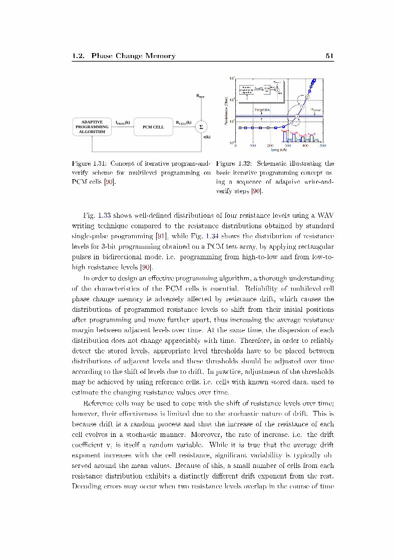
1.2. Phase Change Memory 51
ADAPTIVE PROGRAMMING
ALGORITHMPCM CELL Σ
IPROG(k) RCELL(k)
RREF
e(k)
Figure 1.31: Concept of iterative program-and-
verify scheme for multilevel programming on
PCM cells [90].
Figure 1.32: Schematic illustrating the
basic iterative programming concept us-
ing a sequence of adaptive write-and-
verify steps [90].
Fig. 1.33 shows well-dened distributions of four resistance levels using a WAV
writing technique compared to the resistance distributions obtained by standard
single-pulse programming [91], while Fig. 1.34 shows the distribution of resistance
levels for 3-bit programming obtained on a PCM test array, by applying rectangular
pulses in bidirectional mode, i.e. programming from high-to-low and from low-to-
high resistance levels [90].
In order to design an eective programming algorithm, a thorough understanding
of the characteristics of the PCM cells is essential. Reliability of multilevel-cell
phase change memory is adversely aected by resistance drift, which causes the
distributions of programmed resistance levels to shift from their initial positions
after programming and move further apart, thus increasing the average resistance
margin between adjacent levels over time. At the same time, the dispersion of each
distribution does not change appreciably with time. Therefore, in order to reliably
detect the stored levels, appropriate level thresholds have to be placed between
distributions of adjacent levels and these thresholds should be adjusted over time
according to the shift of levels due to drift. In practice, adjustment of the thresholds
may be achieved by using reference cells, i.e. cells with known stored data, used to
estimate the changing resistance values over time.
Reference cells may be used to cope with the shift of resistance levels over time;
however, their eectiveness is limited due to the stochastic nature of drift. This is
because drift is a random process and thus the increase of the resistance of each
cell evolves in a stochastic manner. Moreover, the rate of increase, i.e. the drift
coecient v, is itself a random variable. While it is true that the average drift
exponent increases with the cell resistance, signicant variability is typically ob-
served around the mean values. Because of this, a small number of cells from each
resistance distribution exhibits a distinctly dierent drift exponent from the rest.
Decoding errors may occur when two resistance levels overlap in the course of time
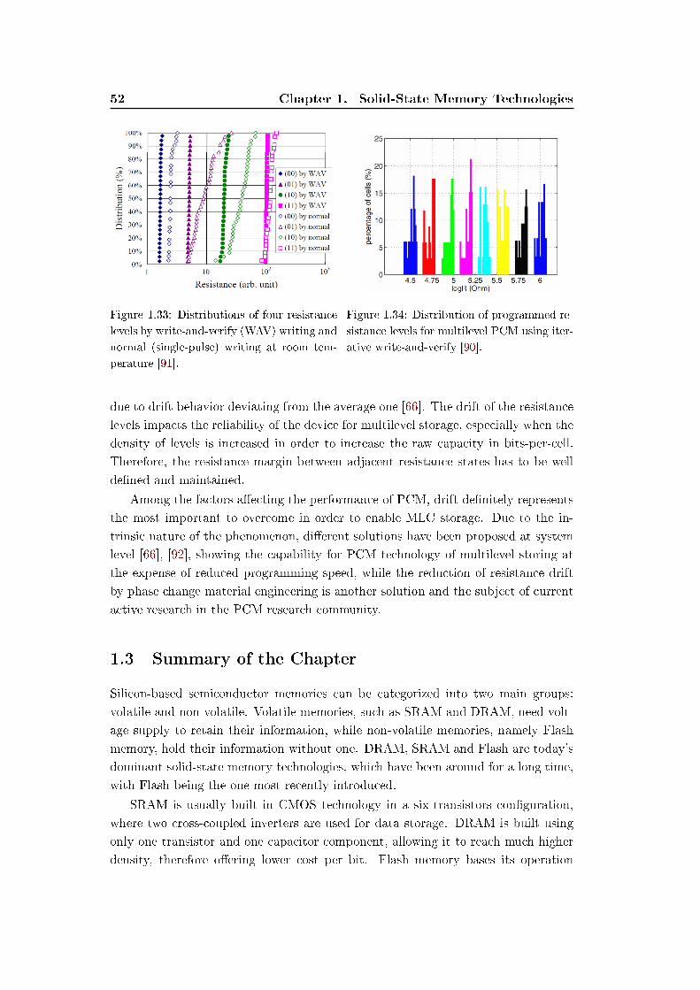
52 Chapter 1. Solid-State Memory Technologies
Figure 1.33: Distributions of four resistance
levels by write-and-verify (WAV) writing and
normal (single-pulse) writing at room tem-
perature [91].
Figure 1.34: Distribution of programmed re-
sistance levels for multilevel PCM using iter-
ative write-and-verify [90].
due to drift behavior deviating from the average one [66]. The drift of the resistance
levels impacts the reliability of the device for multilevel storage, especially when the
density of levels is increased in order to increase the raw capacity in bits-per-cell.
Therefore, the resistance margin between adjacent resistance states has to be well
dened and maintained.
Among the factors aecting the performance of PCM, drift denitely represents
the most important to overcome in order to enable MLC storage. Due to the in-
trinsic nature of the phenomenon, dierent solutions have been proposed at system
level [66], [92], showing the capability for PCM technology of multilevel storing at
the expense of reduced programming speed, while the reduction of resistance drift
by phase change material engineering is another solution and the subject of current
active research in the PCM research community.
1.3 Summary of the Chapter
Silicon-based semiconductor memories can be categorized into two main groups:
volatile and non-volatile. Volatile memories, such as SRAM and DRAM, need volt-
age supply to retain their information, while non-volatile memories, namely Flash
memory, hold their information without one. DRAM, SRAM and Flash are today's
dominant solid-state memory technologies, which have been around for a long time,
with Flash being the one most recently introduced.
SRAM is usually built in CMOS technology in a six-transistors conguration,
where two cross-coupled inverters are used for data storage. DRAM is built using
only one transistor and one capacitor component, allowing it to reach much higher
density, therefore oering lower cost per bit. Flash memory bases its operation
1.3. Summary of the Chapter 53
on a oating gate component. Flash is further divided into two categories: NOR,
characterized by a direct write and a large cell size and NAND, characterized by a
page write and small cell size.
Non-volatile memories are highly reliable and can be programmed using a simple
microcomputer. They can be found virtually in every modern electronic equipment.
Emerging non-volatile memories have always captivated the interest of research and
their potential to be used as a Universal Memory in data systems is undeniable.
The main contenders among the emerging non-volatile memory concepts are MRAM,
FeRAM, PCM and ReRAM. Among them, PCM seems to be the memory technology
that has made rapid progress in a short time, leaving behind older technologies in
terms of sophisticated demonstrations of scaling to small device dimensions. More-
over, it has shown promise to succeed conventional memory technologies, such as
Flash memory and thus play a broad role in the entire storage hierarchy.
PCM bases its operation on a reversible phase transition between the amorphous
and the crystalline phase of a chalcogenide material, usually Ge2Sb2Te5 (GST) or
GeTe, which have been extensively used for optical recording media. The resistance
of a phase change material can be modied by applying an appropriate voltage or
current pulse capable of providing a temperature gradient in the active region of
the cell, thus modifying the material organization between an amorphous and a
crystalline phase. The amorphous region inside the phase change layer can be crys-
tallized by applying SET pulses, increasing the device conductance. The magnitude
of the relative increase in conductance can be controlled by the pulse amplitude
and by the equivalent pulse width. Amorphization, on the other hand is a more
power-hungry process and is not progressive with identical pulses.
The crystalline phase of the phase change material represents the Low Resis-
tance State. The main mechanisms resulting in a crystalline phase are nucleation
and growth, which directly impact the performance of a PCM device, in particular
in terms of speed of the SET programming operation. The amorphous phase of
the phase change materials corresponds to the High Resistance State and has been
largely studied in order to understand the origin of the electronic switching phe-
nomenon, which consists the base of PCM programming as well as the eects of the
structural relaxation of the amorphous phase on the device performance.
Despite the fact that structural relaxation of the amorphous phase leads to re-
sistivity drift, which consists of a resistance increase over time, this phenomenon
does not seem to aect the reliability of the technology when a memory cell is pro-
grammed in the SET or the RESET state. However, for Multilevel Cell applications,
the mechanisms behind this phenomenon need to be fully understood. Another pos-
sible problem that PCM technology might face, concerns the high current density
needed to perform a RESET operation. Luckily, decrease of the cell size results in
a consequent current density decrease. A further reliability issue of this technol-
54 Chapter 1. Solid-State Memory Technologies
ogy is the thermal stability of the amorphous phase at high temperatures, which
might prevent PCM from addressing automotive applications, where the working
temperature ranges up to 150 C.
Nonetheless, despite all the problems PCM might face, it always remains the
most mature among emerging non-volatile memory concepts. PCM has reached a
scalability level beyond that of other memory technologies and has demonstrated
its suitability for embedded applications, thus rendering itself an already conrmed
industrial reality. The range of applications in which it can replace Flash mem-
ory is wide; PCM can be competitive against established memory technologies,
demonstrating potential to be used as execution memory in embedded systems and
computing platforms. At the same time, the wide resistance dierence between the
SET and the RESET state allows it to store more than one bit of digital data per
cell, thus increasing its density and reducing its cost per bit.
Chapter 2
Performance Optimization of
Phase Change Memory
Memories are becoming increasingly fundamental in electronic systems thanks to
the shift from computer-centric to data-centric servers, where the bottlenecks are
expected to be storage and I/O connections. One of the key challenges to sustain this
development is the optimization of the energy consumption of portable devices and
databases. Emerging memory technologies capable of delivering better performance
while consuming less power could play a key role in future IT development.
Phase Change Memory provides an attractive set of features, which is quite inter-
esting for novel applications, while its ability to match the cost of existing memory
technologies and provide a good perspective in terms of scalability makes PCM a
promising candidate to enter a well established memory market. Nevertheless, one
of the key challenges of PCM cell scaling is power reduction, mainly due to the
programming current.
Most of the development has focused on the cell architecture optimization in or-
der to increase programming eciency, however, it has been shown that it is possible
to reduce the programming current of a standard PCM cell by proper material en-
gineering. The reliability optimization of PCM devices based on alternative to GST
materials is the focus of the present Chapter. Through a series of extensive char-
acterization tests, we studied the reliability enhancement thanks to an innovative
N-doped Ge-rich chalcogenide material.
This Chapter starts with a description of the procedure followed for the ex-
perimental testing of state-of-the-art PCM devices. The main electrical parameters
which are of great interest for the scope of this work are introduced, while the device
behavior is discussed in depth. Then, the equipment used to perform the electrical
measurements is briey introduced. Later on, the main reliability issues of PCM
technology are examined and the benets of Material Engineering on the device
performance are introduced. Finally, the results of our extensive characterization
on PCM devices are explained in depth and an innovative pulse sequence, capable
of providing optimal programming conditions in industrially compatible times, is
introduced.
56 Chapter 2. Performance Optimization of Phase Change Memory
2.1 Electrical Characterization of the PCM Cell
The study of the electrical behavior of highly scaled PCM devices and the evalua-
tion of their electrical performance necessitates the use of equipment enabling pulse
widths of few ns combined with a high output slew rate. The latter is fundamental
to allow rise and fall times of a few ns to quench the molten phase change material,
which is needed to program the memory device in its RESET state.
At the same time, the wide programming window PCM devices demonstrate,
which in some cases exceeds three orders of magnitude, requires a highly accurate
sensing for all possible resistance states in which the cell can be programmed. In
order to be able to perform statistical analysis and model the behavior of devices, a
large number of tests on a broad number of devices is required, which emphasizes the
need for a fast and fully automatic characterization system. Furthermore, electrical
characterization performed at high temperature must be equally reliable as the one
performed at room temperature. In the following paragraphs, we will introduce
the main electrical parameters taken into account during the experimental tests, as
well as the devices and the setup used for our experimental analysis. We will then
focus on the main reliability issues typical of a phase change memory cell and the
procedures used during our tests to evaluate these aspects in our devices.
2.1.1 Main Electrical Parameters
A Phase Change Memory cell is a two-terminal device, which bases its functionality
on the strong resistivity dierence between the amorphous and the crystalline phase.
In order to model the electrothermal behavior of the cell, the properties of each
phase of the chalcogenide material have to be taken into account since they give
rise to a specic current-voltage characteristic that depends on the structure of the
device and on the integrated phase change material. To this purpose, a thorough
understanding of the electrical properties of the phase change material is necessary.
Fig. 2.1 shows a typical I-V curve of a PCM device. Starting from the RESET
state (lled dots), the increase in the voltage across the phase change material pro-
duces an increase in the conductivity of the amorphous material, which is conrmed
by the change of the RESET curve slope at voltages higher than 0.5 V. Once the
threshold voltage VTH is reached, threshold switching occurs, as indicated by the
voltage snap back. The device is in the ON state and while being in a SET range
of currents, it can reach temperatures favorable for recrystallization, achieving a
SET state once the pulse is removed. If the current provided is higher than this
range (approaching the melting current IM), the phase change material melts and
depending on the slope of the pulse trailing edge, it can either preserve its amor-
phous structure (abrupt quenching) or recrystallize (long fall time). An increase in
the conductivity of the phase change material at voltages higher than 0.5 V can also
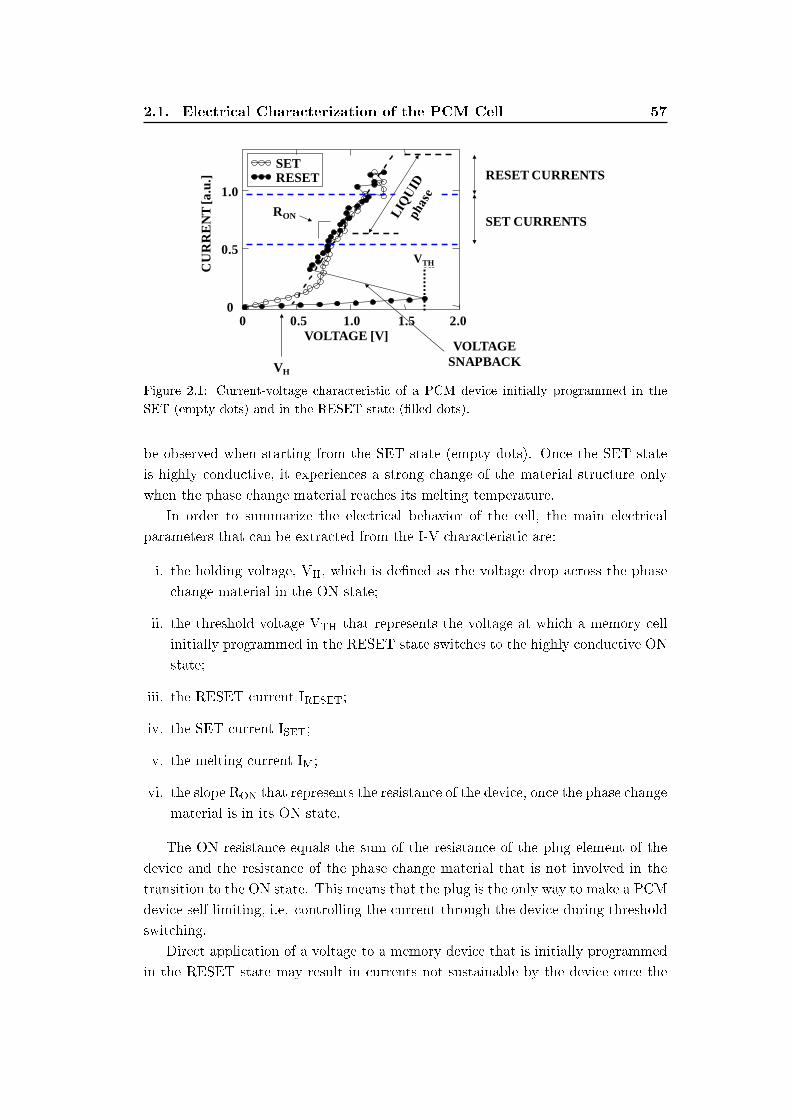
2.1. Electrical Characterization of the PCM Cell 57
0 0.5 1.0 1.5 2.00
0.5
1.0C
UR
RE
NT
[a.u
.]
VOLTAGE [V]
SET CURRENTS
RESET CURRENTS
VTH
VOLTAGESNAPBACK
RESETSET
RON
VH
VTH
Figure 2.1: Current-voltage characteristic of a PCM device initially programmed in the
SET (empty dots) and in the RESET state (lled dots).
be observed when starting from the SET state (empty dots). Once the SET state
is highly conductive, it experiences a strong change of the material structure only
when the phase change material reaches its melting temperature.
In order to summarize the electrical behavior of the cell, the main electrical
parameters that can be extracted from the I-V characteristic are:
i. the holding voltage, VH, which is dened as the voltage drop across the phase
change material in the ON state;
ii. the threshold voltage VTH that represents the voltage at which a memory cell
initially programmed in the RESET state switches to the highly conductive ON
state;
iii. the RESET current IRESET;
iv. the SET current ISET;
v. the melting current IM;
vi. the slope RON that represents the resistance of the device, once the phase change
material is in its ON state.
The ON resistance equals the sum of the resistance of the plug element of the
device and the resistance of the phase change material that is not involved in the
transition to the ON state. This means that the plug is the only way to make a PCM
device self-limiting, i.e. controlling the current through the device during threshold
switching.
Direct application of a voltage to a memory device that is initially programmed
in the RESET state may result in currents not sustainable by the device once the
58 Chapter 2. Performance Optimization of Phase Change Memory
threshold voltage is reached. These currents may lead to device degeneration and,
thus, a memory access device capable of limiting the current owing through the
cell (e.g. a transistor or a diode) is necessary. From the I-V characteristic of the
PCM device, the voltage drop across the cell as a function of the current when the
cell is in the ON state can be described as
VCELL = RONION +VH. (2.1)
The nal power delivered to the device will therefore be
PCELL = RONI2ON +VHION. (2.2)
2.1.2 Thermal Parameters
In the calculation of the power delivered to the cell, it is important to take into
account both voltage contributions, namely the one from the ON resistance (Joule
heating) and the one from the holding voltage. In fact, the latter term is the
real voltage drop across the phase change material layer in the ON state during
programming.
Considering the device from a thermal point of view, the thermal eciency of
the cell is related to the thermal resistance of the PCM cell RTH. As a matter of
fact, we have
∆T = PCELLRTH. (2.3)
When power is provided to a PCM device, a temperature increase, ∆T, is gener-
ated in the phase change material that depends on the structure and on the thermal
conductivity of the materials surrounding the active region of the phase change ma-
terial. Since the power delivered to the cell is used to increase the temperature of
the phase change material, the higher is RTH, the lower is the nal power needed to
achieve the target temperature increment. RTH depends on the thermal conductiv-
ity of the materials that surround the active volume of the phase change material, in
particular, the plug, the interface between the plug and the phase change material
and the crystalline phase of the phase change material that is not involved in the
phase transition [93].
The plug is the metallic element of the PCM device that provides electrical ac-
cess to the phase change material. Its geometry denes the area and the geometry
of the interface between the plug itself and the active volume. The material compo-
sition of the plug as well as its geometry impact the functionality and the thermal
eciency of the memory cell. Its resistance has to be matched with the phase change
material resistivity, in order to optimize the position of the temperature peak at the
plug/phase change material interface [93].
Considering a dierent optimization approach, we can engineer the plug material
while keeping the cell geometry unchanged. The resistivity of the plug can be
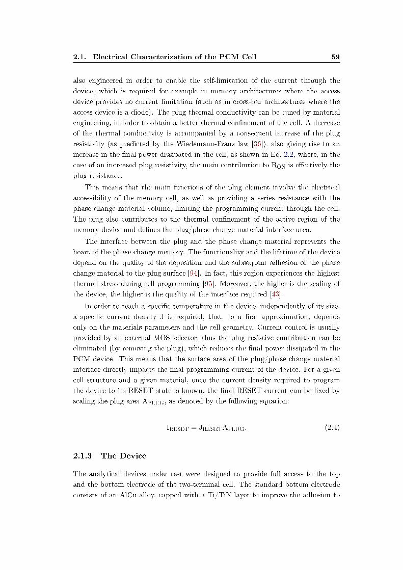
2.1. Electrical Characterization of the PCM Cell 59
also engineered in order to enable the self-limitation of the current through the
device, which is required for example in memory architectures where the access
device provides no current limitation (such as in cross-bar architectures where the
access device is a diode). The plug thermal conductivity can be tuned by material
engineering, in order to obtain a better thermal connement of the cell. A decrease
of the thermal conductivity is accompanied by a consequent increase of the plug
resistivity (as predicted by the Wiedemann-Franz law [36]), also giving rise to an
increase in the nal power dissipated in the cell, as shown in Eq. 2.2, where, in the
case of an increased plug resistivity, the main contribution to RON is eectively the
plug resistance.
This means that the main functions of the plug element involve the electrical
accessibility of the memory cell, as well as providing a series resistance with the
phase change material volume, limiting the programming current through the cell.
The plug also contributes to the thermal connement of the active region of the
memory device and denes the plug/phase change material interface area.
The interface between the plug and the phase change material represents the
heart of the phase change memory. The functionality and the lifetime of the device
depend on the quality of the deposition and the subsequent adhesion of the phase
change material to the plug surface [94]. In fact, this region experiences the highest
thermal stress during cell programming [95]. Moreover, the higher is the scaling of
the device, the higher is the quality of the interface required [43].
In order to reach a specic temperature in the device, independently of its size,
a specic current density J is required, that, to a rst approximation, depends
only on the materials parameters and the cell geometry. Current control is usually
provided by an external MOS selector, thus the plug resistive contribution can be
eliminated (by removing the plug), which reduces the nal power dissipated in the
PCM device. This means that the surface area of the plug/phase change material
interface directly impacts the nal programming current of the device. For a given
cell structure and a given material, once the current density required to program
the device to its RESET state is known, the nal RESET current can be xed by
scaling the plug area APLUG, as denoted by the following equation:
IRESET = JRESETAPLUG. (2.4)
2.1.3 The Device
The analytical devices under test were designed to provide full access to the top
and the bottom electrode of the two-terminal cell. The standard bottom electrode
consists of an AlCu alloy, capped with a Ti/TiN layer to improve the adhesion to
60 Chapter 2. Performance Optimization of Phase Change Memory
VO
LT
AG
E [a
.u.]
TIME [a.u.]
VPULSE
VCELL
VLOAD
VTH
Figure 2.2: General setup used to characterize a PCM cell. The cell current is limited by an
external series resistance (RLOAD). On the right, the waveforms applied to the series of the
cell and the load resistor (VPULSE) and the voltage acquired on the PCM device (VCELL)
are shown. The voltage drop across RLOAD allows calculating the current owing through
the cell during pulse application.
the plug interface, whereas the top electrode is made of copper. The devices under
test are single 1R cells, where no selector is co-integrated with the memory element.
The study of single PCM cells enables the monitoring of the behavior of the
integrated phase change material. All devices under test were fabricated on 200 mm
wafers. The use of single-cell devices as a test vehicle enabled the fabrication of a
large number of devices on a single wafer in order to increase the obtained statistics.
In order to limit the current owing through the PCM device, a load resistance
RLOAD is placed in series with the cell (pull-up conguration - Fig. 2.2). The voltage
drop across the load resistor during the pulse application is acquired through an
oscilloscope in order to calculate the nal current provided to the device, according
to the following equation:
ICELL =VPULSE −VCELL
RLOAD, (2.5)
where VPULSE is the voltage applied to the series of cell and load resistor and VCELL
is the voltage acquired across the PCM device.
The sizing of the external load resistance is fundamental for the study of the
cell and depends on the electrical parameters of the device. The value of the load
resistance needs to ensure that the current required for the RESET operation can
be reached. Since the maximum VPULSE is limited by the maximum voltage that
can be provided by the equipment, the series load resistance has to be adapted
accordingly in order to guarantee that the cell can be programmed to its RESET
state. Moreover, the minimum resolution of the measurement of the voltage drop
across the load resistance has to allow the acquisition of low current values, whereas
2.1. Electrical Characterization of the PCM Cell 61
the value of RLOAD must also guarantee the possibility to screen currents able to
crystallize the cell at the threshold voltage VTH.
In Fig. 2.2 we report an example of the acquired waveforms of the evolution of
the voltage applied, VPULSE and the voltage measured across the cell, VCELL. The
device is initially programmed in the RESET state and, thus, the voltage applied
drops completely across the cell. Once the threshold voltage is reached, the cell
enters its ON state and starts being highly conductive. As a result, the voltage drop
across the cell is reduced and the drop across the load resistance is increased.
Since current limitation is provided externally, a limitation on the bandwidth
is to be expected due to the parasitic capacitance CP of the system. CP results
from the sum of all parasitic contributions of the external cables, the probe needles
used to contact the device electrodes and the capacitance between the top and the
bottom electrode of the device.
During the application of a pulse across a cell in the HRS, CP is charged until
the threshold voltage of the device is reached. The cell then switches to its highly
conductive ON state and the system experiences another transient phenomenon
before recovering its stability (in fact, the nal voltage across the cell will be lower
than VTH). CP discharges on the parallel connection of the cell and RLOAD, thus
giving rise to a peak of current through the device that is approximately equal to
IPEAK = VTHRON. (2.6)
RON includes the resistive contributions of all the elements of the device, in
particular the resistance of the plug RPLUG, the resistance contribution of the top
and the bottom electrode and the relative access lines, RLINES, and the resistance of
the phase change material that, after the switching event, is taken to its ON state.
The recovery of the stability in the cell is provided after a characteristic time,
which is proportional to CP. This recovery transient can represent a source of
thermal stress for the cell, therefore adversely aecting its endurance performance.
A proper reduction of CP can reduce the impact of this phenomenon. As we will
see, in order to increase the bandwidth of the programming system and reduce the
transients duration, an innovative pulse sequence was engineered. The co-integration
of the PCM elements with the testing circuit that will be the focus of the following
Chapter, has the purpose to eliminate the main parasitic distributions that aect
system performance.
62 Chapter 2. Performance Optimization of Phase Change Memory
2.1.4 The Equipment
The electrical characterization of a PCM device consists of three main parts:
i. the application of a voltage/current on the device;
ii. the sensing;
iii. the nal acquisition of data.
For voltage generation, an Agilent 81110A pulse/pattern generator capable of
2 ns transition time and 5 ns pulse width was used. The generator enables the
application of trains of pulses as well as of combined pulses (e.g. sum of two dierent
pulses) and the tuning of the fall time of the pulse independently from its rise time.
To acquire the pulses applied to the cell, we used a 2 GS/s oscilloscope Tektronix
TDS 744A, combined with two active probes P6205 (750 MHz). To guarantee a high
accuracy in the sensing of the cell, we used a parametric analyser (such as Agilent
4156C and Keithley 4200-SCS) with a veried current sensing resolution of 10 pA (in
the nal test conguration). To automatically move the probe needles and contact
the devices under test, a Cascade Microtech probe station was employed, equipped
with a hot chuck with temperature remote control capability up to 300 C.
In order to automatize all the electrical characterization process, a highly inno-
vative electronic board was used, which enables the change of RLOAD by remotely
controlling of the load resistance during the characterization procedure as well as
the switching between the pulse generation electronics. The change of the load re-
sistance during characterization is required in order to rene the current control in
the range of currents favorable to crystallization.
The control of the equipment was realized under Labview and C code program-
ming environment. The nal hardware/software system enabled standard charac-
terization procedures (low-eld measurements, programming characteristics, data
retention, cycling, etc.) and the engineering of new procedures for the study of the
behavior of new materials integrated in PCM devices.
Fig. 2.3 shows an example of the output of the characterization system: a
staircase-up (SCU) procedure is a train of pulses with increasing amplitude and
can be a useful tool to verify cell functionality. The cell starts in the RESET state
and then switches to the SET state once the threshold voltage VTH is reached. In-
creasing the current, the cell resistance gradually increases until the original RESET
state is recovered.
From the acquisition of the current provided to the cell during each pulse, the
voltage drop across the cell and the resistance of the device measured after each
pulse, we can construct a full R-I-V programming characteristic for any given pulse
width. From this curve, we can obtain the standard R-I and I-V characteristics that
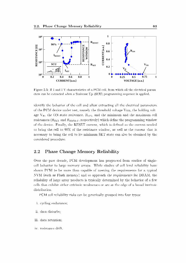
2.2. Phase Change Memory Reliability 63
106
105
104
103
0 0.2 0.4 0.6 0.8 1
RE
SIST
AN
CE
[Ω]
CURRENT [a.u.]
RRESET
RSET
RE
SIST
AN
CE
W
IND
OW
90%
IRESET
ISET...
SCU
0 0.25 0.5 0.75 10
0.2
1
CU
RR
EN
T [a
.u.]
VOLTAGE [a.u.]
VTH
VH
RON
0.4
0.6
0.8
Figure 2.3: R-I and I-V characteristics of a PCM cell, from which all the electrical param-
eters can be extracted when a Staircase Up (SCU) programming sequence is applied.
identify the behavior of the cell and allow extracting all the electrical parameters
of the PCM device under test, namely the threshold voltage VTH, the holding volt-
age VH, the ON state resistance, RON, and the minimum and the maximum cell
resistances (RSET and RRESET, respectively) which dene the programming window
of the device. Finally, the RESET current, which is dened as the current needed
to bring the cell to 90% of the resistance window, as well as the current that is
necessary to bring the cell to its minimum SET state can also be obtained by the
considered procedure.
2.2 Phase Change Memory Reliability
Over the past decade, PCM development has progressed from studies of single-
cell behavior to large memory arrays. While studies of cell level reliability have
shown PCM to be more than capable of meeting the requirements for a typical
NVM (such as Flash memory) and to approach the requirements for DRAM, the
reliability of large array products is typically determined by the behavior of a few
cells that exhibit either extrinsic weaknesses or are at the edge of a broad intrinsic
distribution.
PCM cell reliability risks can be generically grouped into four types:
i. cycling endurance;
ii. data disturbs;
iii. data retention;
iv. resistance drift.
64 Chapter 2. Performance Optimization of Phase Change Memory
Cycling endurance is the number of re-write operations that can be applied to the
cell without failure. Data disturb concerns the ability to access a cell or neighboring
cells without unintentionally changing the stored data. Data retention refers to the
ability of the device to retain the data written into the cell over a period of time and
typically at a maximum ambient temperature. Resistance drift involves the low-eld
resistance increase over time and is mainly attributed to the structural relaxation
of the amorphous phase of a chalcogenide material.
The majority of these reliability issues of PCM technology are related to the
working temperature of the device. However, some of them are not exclusively
related to temperature, but also to a combination of temperature with other pa-
rameters such as sub-threshold switching that depends on the electric eld applied
to the cell or material segregation, that depends on the atomic composition.
The working temperature strongly aects the device performance. First of all,
temperature can impact the retention of the information stored in a PCM device
through recrystallization of the amorphous chalcogenide. However, the recrystal-
lization mechanism is not the only issue that can inuence the thermal stability
of a phase change material (in particular, a phase change material is aected by
the temperature activated structural relaxation phenomenon that gives rise to the
resistance drift toward higher resistance values). Even when the working temper-
ature is lower than the critical crystallization temperature, the cell can experience
an unwanted increase of the temperature due to the programming of neighboring
devices (crosstalk phenomenon).
PCM performs well in each of these areas. It shows data retention capability for
cells based on Ge2Sb2Te5 (GST) greater than 10 years at 85 C [31], [42], [96], [97],
independently of prior cycling. Floating gate devices, instead, show a reduction
in retention as they are cycled. Cycling counts exceeding 1012 have been reported
for isolated cells and 109 for cells integrated in full arrays. In addition, read and
proximity disturb characterization has shown the capability of continuous reading
for 10 years and 1010 write operations on surrounding cells [42]. Finally, resistance
drift seems to be aecting only the RESET state of PCM cells based on conventional
GST material and is generally well documented and understood in the literature.
In addition to its ability to lithographically scale, these characteristics make
PCM an attractive candidate for both traditional applications and for applications
that had previously been beyond the capability of oating gate devices. At cell level,
data retention and disturb risk are primarily conned to the RESET state due to the
fact that the amorphous state is metastable with respect to the stable crystalline
phase. Any additional energy applied to this state (primarily in thermal and/or
electrical form) can accelerate the crystallization process. For data retention, this
energy is thermal and provided by the surrounding ambient.
2.2. Phase Change Memory Reliability 65
2.2.1 Cycling Endurance
Achieving high reliability for cycling endurance also requires optimized device op-
eration. At cell level, two modes of cycling failures are observed: cell opens (stuck
RESET) and RESET fails (stuck SET). Analysis of failed cells shows that they
have dierent electrical characteristics prior to cycling, which may give clues as to
the nature of the failures.
In general, cells that become open after cycling show a higher threshold voltage
than cells that do not fail, suggesting a failure mechanism related to the phase change
material. Cells that show RESET fail, instead, show matched threshold voltages but
a high resistance (dV/dI) in the I-V curve at high current. This suggests that the
failure mechanism is related to the heating element. Subsequent physical failure
analysis conrms these hypotheses, showing evidence for the generation of voids in
the chalcogenide material above the heater for the open cells and Ge contamination
of the heater in the RESET fails. In the latter case, Ge contamination reduces
heater eciency, thus preventing a suciently large volume of GST from melting
during the programming operation. The resulting amorphous region is then too
small to achieve the required high resistance.
An advantage of PCM over oating gate technologies is that cycling a PCM
device does not show a subsequent reduction in data retention. In Flash devices,
repeated programming and erasing of the cell damages the tunnel oxide and re-
duces data retention [98]. The cell failure rate decreases with increasing prior cycles
observed in PCM suggests that the chemical composition changes that may take
place in GST during programming [99] do not reduce the thermal stability of the
amorphous state.
Moreover, one factor that can impact the nal lifetime of the PCM device is the
scaling of the plug/phase change material interface due to thermal stress generated
during programming. During the RESET pulse, the phase change material reaches
its melting temperature and, even if the pulse is applied for merely a few ns, the
cumulative eect can generate mechanical failures such as delamination, cracks, local
stoichiometry changes, materials interdiusion, etc. [100].
The general trend observed in the literature highlights the increasing importance
of the engineering of the interfaces/materials and the optimization of the deposition
quality of the phase change material as the dimension of the active area of the PCM
device decreases. To be competitive with other emerging technologies, the scaling
of the PCM device must go hand in hand with the preserving of the cyclability
performance.
Endurance tests on PCM devices can be performed by providing sequences of
repeated SET and RESET pulses, stopping the train of pulses at predetermined
logarithmically spaced time steps to verify the functionality of the cell and evaluate
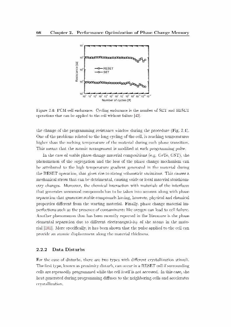
66 Chapter 2. Performance Optimization of Phase Change Memory
Figure 2.4: PCM cell endurance. Cycling endurance is the number of SET and RESET
operations that can be applied to the cell without failure [42].
the change of the programming resistance window during the procedure (Fig. 2.4).
One of the problems related to the long cycling of the cell, is reaching temperatures
higher than the melting temperature of the material during each phase transition.
This means that the atomic arrangement is modied at each programming pulse.
In the case of stable phase change material compositions (e.g. GeTe, GST), the
phenomenon of the segregation and the loss of the phase change mechanism can
be attributed to the high temperature gradient generated in the material during
the RESET operation, that gives rise to strong volumetric variations. This causes a
mechanical stress that can be detrimental, causing voids or local material stoichiom-
etry changes. Moreover, the chemical interaction with materials of the interfaces
that generates unwanted compounds has to be taken into account along with phase
separation that generates stable compounds having, however, physical and chemical
properties dierent from the starting material. Finally, phase change material im-
perfections such as the presence of contaminants like oxygen can lead to cell failure.
Another phenomenon that has been recently reported in the literature is the phase
elemental separation due to dierent electronegativity of the atoms in the mate-
rial [101]. More specically, it has been shown that the pulse applied to the cell can
provide an atomic displacement along the material thickness.
2.2.2 Data Disturbs
For the case of disturbs, there are two types with dierent crystallization stimuli.
The rst type, known as proximity disturb, can occur in a RESET cell if surrounding
cells are repeatedly programmed while the cell itself is not accessed. In this case, the
heat generated during programming diuses to the neighboring cells and accelerates
crystallization.
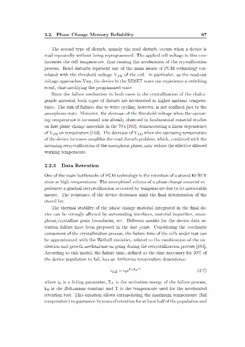
2.2. Phase Change Memory Reliability 67
The second type of disturb, namely the read disturb, occurs when a device is
read repeatedly without being reprogrammed. The applied cell voltage in this case
increases the cell temperature, thus causing the acceleration of the crystallization
process. Read disturbs represent one of the main issues of PCM technology cor-
related with the threshold voltage VTH of the cell. In particular, as the read-out
voltage approaches VTH, the device in the RESET state can experience a switching
event, thus modifying the programmed state.
Since the failure mechanism in both cases is the crystallization of the chalco-
genide material, both types of disturb are accelerated at higher ambient tempera-
tures. The risk of failures due to write cycling, however, is not conned just to the
amorphous state. Moreover, the decrease of the threshold voltage when the operat-
ing temperature is increased was already observed in fundamental material studies
on rst phase change materials in the 70's [102], demonstrating a linear dependence
of VTH on temperature [103]. The decrease of VTH when the operating temperature
of the device increases amplies the read disturb problem, which, combined with the
incoming recrystallization of the amorphous phase, may reduce the eective allowed
working temperature.
2.2.3 Data Retention
One of the main bottlenecks of PCM technology is the retention of a stored RESET
state at high temperatures. The amorphized volume of a phase change material ex-
periences a gradual recrystallization activated by temperature due to its metastable
nature. The resistance of the device decreases until the nal deterioration of the
stored bit.
The thermal stability of the phase change material integrated in the nal de-
vice can be strongly aected by surrounding interfaces, material impurities, amor-
phous/crystalline grain boundaries, etc. Dierent models for the device data re-
tention failure have been proposed in the last years. Considering the stochastic
component of the crystallization process, the failure time of the cells under test can
be approximated with the Weibull statistics, related to the combination of the nu-
cleation and growth mechanisms on going during the recrystallization process [104].
According to this model, the failure time, dened as the time necessary for 50% of
the device population to fail, has an Arrhenius temperature dependence:
tfail = t0eEAkBT (2.7)
where t0 is a tting parameter, EA is the activation energy of the failure process,
kB is the Boltzmann constant and T is the temperature used for the accelerated
retention test. This equation allows extrapolating the maximum temperature (fail
temperature) to guarantee 10 years of retention for at least half of the population and
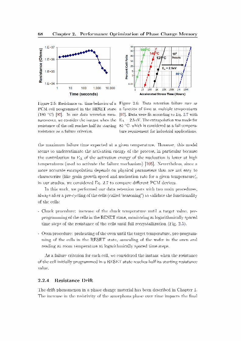
68 Chapter 2. Performance Optimization of Phase Change Memory
Figure 2.5: Resistance vs. time behavior of a
PCM cell programmed in the RESET state
(180 C) [97]. In our data retention mea-
surements, we consider the instant when the
resistance of the cell reaches half its starting
resistance as a failure criterion.
Figure 2.6: Data retention failure rate as
a function of time at multiple temperatures
[97]. Data were t according to Eq. 2.7 with
EA = 2.5 eV. The extrapolation was made for
85 C, which is considered as a fail tempera-
ture requirement for industrial applications.
the maximum failure time expected at a given temperature. However, this model
seems to underestimate the activation energy of the process, in particular because
the contribution to EA of the activation energy of the nucleation is lower at high
temperatures (used to activate the failure mechanism) [105]. Nevertheless, since a
more accurate extrapolation depends on physical parameters that are not easy to
characterize (like grain growth speed and nucleation rate for a given temperature),
in our studies, we considered Eq. 2.7 to compare dierent PCM devices.
In this work, we performed our data retention tests with two main procedures,
always after a pre-cycling of the cells (called seasoning) to validate the functionality
of the cells:
- Chuck procedure: increase of the chuck temperature until a target value, pre-
programming of the cells in the RESET state, monitoring at logarithmically spaced
time steps of the resistance of the cells until full recrystallization (Fig. 2.5).
- Oven procedure: preheating of the oven until the target temperature, pre-program-
ming of the cells in the RESET state, annealing of the wafer in the oven and
reading at room temperature at logarithmically spaced time steps.
As a failure criterion for each cell, we considered the instant when the resistance
of the cell initially programmed in a RESET state reaches half its starting resistance
value.
2.2.4 Resistance Drift
The drift phenomenon in a phase change material has been described in Chapter 1.
The increase in the resistivity of the amorphous phase over time impacts the nal
2.3. Phase Change Material Engineering 69
stability of the programmed state in the cell but this phenomenon does not represent
a problem in a nal device, since the crystalline phase does not experience this
problem. Even though the RESET state drifts towards higher resistance values, the
SET state is substantially stable and a threshold resistance to discriminate the two
states can be found.
Moreover, the higher is the resistance of the cell, the higher is the drift coecient
ν [57], calculated according to equation
R = R0(tt0)ν. (2.8)
The problem of the resistance drift becomes detrimental in Multilevel Cell ap-
plications, where the cell is programmed to intermediate resistance states. This
requires ecient programming and reading techniques at system level, to ensure
storage reliability [90]. At the same time, experimental results also show how the
drift phenomenon broadens the resistance dispersion of the devices when the resis-
tance value increases [66].
2.3 Phase Change Material Engineering
Phase change material properties are known to inuence PCM device parameters
such as the crystallization temperature, having an eect on data retention and
lifetime, while resistivity values of the amorphous and crystalline phases impact the
current/voltage needed to program the cell.
Ge2Sb2Te5 (GST) is recognized as the reference chalcogenide material for stan-
dard PCM in consumer market applications. One of the most critical bottlenecks
of Ge2Sb2Te5 is its low crystallization temperature (≈ 150 C) that makes it in-
trinsically impossible to satisfy the standard 85 C 10-years data retention require-
ments [106].
In the last years, many eorts have been put in the research of new materials
and the study of their properties to target automotive applications, for which the
operating temperature is in the range of 150 C. To address this requirement, dier-
ent approaches at material level are possible. A rst one mainly consists in changing
the stoichiometry of Ge2Sb2Te5 or adding dopants to increase the stability of the
amorphous state [107]. Another solution is to look for dierent materials with a
higher crystallization temperature.
Material Engineering of chalcogenide alloys used in Phase Change Memory ap-
plication can drastically improve device characteristics. Addition of dopants is an
eective way of changing the characteristics of phase change materials, leading to
an overall performance optimization of the technology. Table 2.1 summarizes the
inuence that material parameters have on PCM performance.
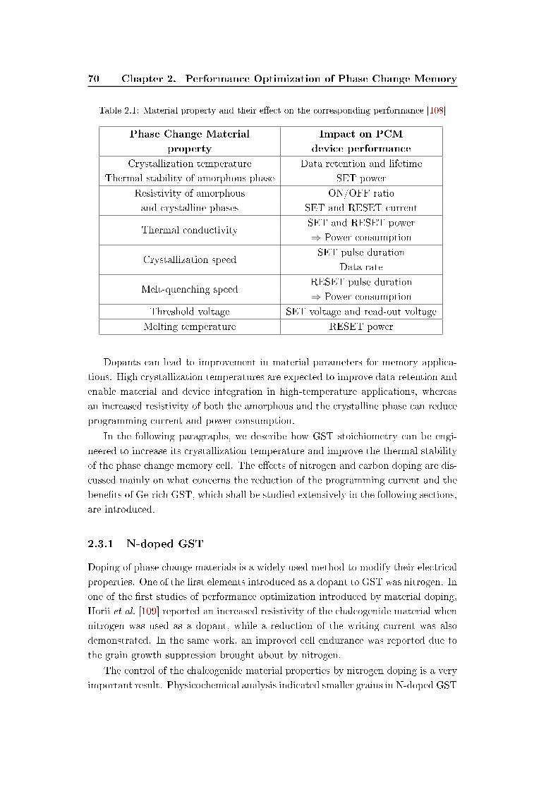
70 Chapter 2. Performance Optimization of Phase Change Memory
Table 2.1: Material property and their eect on the corresponding performance [108]
Phase Change Material Impact on PCM
property device performance
Crystallization temperature Data retention and lifetime
Thermal stability of amorphous phase SET power
Resistivity of amorphous ON/OFF ratio
and crystalline phases SET and RESET current
Thermal conductivitySET and RESET power
⇒ Power consumption
Crystallization speedSET pulse duration
Data rate
Melt-quenching speedRESET pulse duration
⇒ Power consumption
Threshold voltage SET voltage and read-out voltage
Melting temperature RESET power
Dopants can lead to improvement in material parameters for memory applica-
tions. High crystallization temperatures are expected to improve data retention and
enable material and device integration in high-temperature applications, whereas
an increased resistivity of both the amorphous and the crystalline phase can reduce
programming current and power consumption.
In the following paragraphs, we describe how GST stoichiometry can be engi-
neered to increase its crystallization temperature and improve the thermal stability
of the phase change memory cell. The eects of nitrogen and carbon doping are dis-
cussed mainly on what concerns the reduction of the programming current and the
benets of Ge-rich GST, which shall be studied extensively in the following sections,
are introduced.
2.3.1 N-doped GST
Doping of phase change materials is a widely used method to modify their electrical
properties. One of the rst elements introduced as a dopant to GST was nitrogen. In
one of the rst studies of performance optimization introduced by material doping,
Horii et al. [109] reported an increased resistivity of the chalcogenide material when
nitrogen was used as a dopant, while a reduction of the writing current was also
demonstrated. In the same work, an improved cell endurance was reported due to
the grain growth suppression brought about by nitrogen.
The control of the chalcogenide material properties by nitrogen doping is a very
important result. Physicochemical analysis indicated smaller grains in N-doped GST
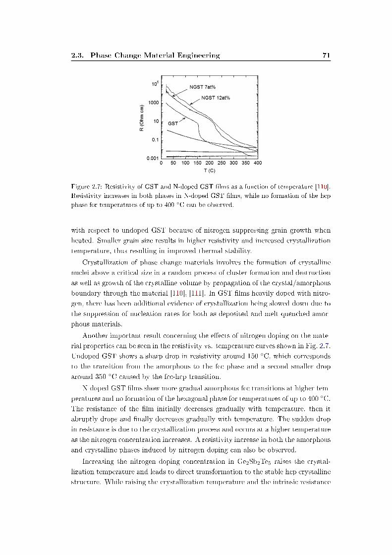
2.3. Phase Change Material Engineering 71
Figure 2.7: Resistivity of GST and N-doped GST lms as a function of temperature [110].
Resistivity increases in both phases in N-doped GST lms, while no formation of the hcp
phase for temperatures of up to 400 C can be observed.
with respect to undoped GST because of nitrogen suppressing grain growth when
heated. Smaller grain size results in higher resistivity and increased crystallization
temperature, thus resulting in improved thermal stability.
Crystallization of phase change materials involves the formation of crystalline
nuclei above a critical size in a random process of cluster formation and destruction
as well as growth of the crystalline volume by propagation of the crystal/amorphous
boundary through the material [110], [111]. In GST lms heavily doped with nitro-
gen, there has been additional evidence of crystallization being slowed down due to
the suppression of nucleation rates for both as-deposited and melt-quenched amor-
phous materials.
Another important result concerning the eects of nitrogen doping on the mate-
rial properties can be seen in the resistivity vs. temperature curves shown in Fig. 2.7.
Undoped GST shows a sharp drop in resistivity around 150 C, which corresponds
to the transition from the amorphous to the fcc phase and a second smaller drop
around 350 C caused by the fcc-hcp transition.
N-doped GST lms show more gradual amorphous-fcc transitions at higher tem-
peratures and no formation of the hexagonal phase for temperatures of up to 400 C.
The resistance of the lm initially decreases gradually with temperature, then it
abruptly drops and nally decreases gradually with temperature. The sudden drop
in resistance is due to the crystallization process and occurs at a higher temperature
as the nitrogen concentration increases. A resistivity increase in both the amorphous
and crystalline phases induced by nitrogen doping can also be observed.
Increasing the nitrogen doping concentration in Ge2Sb2Te5 raises the crystal-
lization temperature and leads to direct transformation to the stable hcp crystalline
structure. While raising the crystallization temperature and the intrinsic resistance
72 Chapter 2. Performance Optimization of Phase Change Memory
of the material by nitrogen doping are eective approaches to enhance thermal sta-
bility and reduce the RESET current, excessive nitrogen incorporation could lead
to adverse results. Transformation to the metastable fcc phase appears to be an
essential criterion to achieve low programming currents and maintain fast switching
properties. Therefore, a careful consideration of various factors points towards a
nitrogen doping concentration of 3 to 4 atomic percentage in Ge2Sb2Te5 lms to
achieve good device performance.
2.3.2 C-doped GST
Phase Change Memory has the potential to act as a promising candidate for the
emerging Storage Class Memory, given its power eciency and continuous storage
capacity improvement through scaling, along with its fast programming speed and
sucient data retention. For highly scaled PCM devices, however, several issues
have to be addressed to provide highly reliable devices, suitable for mobile memory
applications.
One of the main bottlenecks that prevent PCM from being commercially viable
for embedded applications is the large current needed to amorphize the active region
of the phase change material through the melt-quench process. The high current
required for the transition from the SET to the RESET state limits the minimum
size of the selector element and, hence, the maximum memory density and therefore
needs to be lowered in order to reduce power consumption. Moreover, the low
crystallization temperature of Ge2Sb2Te5 leads to stability problems related to the
amorphous phase and consequent poor data retention capability. These problems
need to be addressed since thermal cross-talk between adjacent memory cells can be
relatively severe in high-density memory arrays. A higher stability of the amorphous
phase to boost the data retention performance of PCM is thus necessary.
So far, many studies have been carried out to solve these issues by either experi-
mental methods or theoretical calculations, with the incorporated dopants including
N, O [112] and SiO2 [113]. The addition of these elements to GST leads to larger
resistivity of the crystalline phase with a benecial reduction of the write current,
along with a signicantly improved retention time of the amorphous phase due to
an increased crystallization temperature.
The impact of carbon on the atomic and electronic properties of amorphous GST
has been proven more eective than the dopants mentioned above. Carbon doping
was found to aect the local order of the amorphous structure of GST by increasing
the contribution of tetrahedral Ge atoms [114] while, at the same time, the energy
required for the amorphization of the crystalline material can be largely decreased
by reducing the active volume and conning the phase change material.
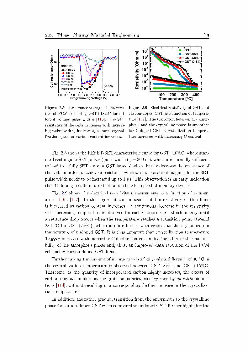
2.3. Phase Change Material Engineering 73
Figure 2.8: Resistance-voltage characteris-
tics of PCM cell using GST+18%C for dif-
ferent voltage pulse widths [115]. The SET
resistance of the cells decreases with increas-
ing pulse width, indicating a lower crystal-
lization speed as carbon content increases.
Figure 2.9: Electrical resistivity of GST and
carbon-doped GST as a function of tempera-
ture [107]. The transition between the amor-
phous and the crystalline phase is smoother
for C-doped GST. Crystallization tempera-
ture increases with increasing C content.
Fig. 2.8 shows the RESET-SET characteristic curve for GST+10%C, where stan-
dard rectangular SET pulses (pulse width tw = 300 ns), which are normally sucient
to lead to a fully SET state in GST-based devices, barely decrease the resistance of
the cell. In order to achieve a resistance window of one order of magnitude, the SET
pulse width needs to be increased up to 1 µs. This observation is an early indication
that C-doping results in a reduction of the SET speed of memory devices.
Fig. 2.9 shows the electrical resistivity measurements as a function of temper-
ature [116], [107]. In this gure, it can be seen that the resistivity of thin lms
is increased as carbon content increases. A continuous decrease in the resistivity
with increasing temperature is observed for each C-doped GST stoichiometry, until
a resistance drop occurs when the temperature reaches a transition point (around
280 C for GST+5%C), which is quite higher with respect to the crystallization
temperature of undoped GST. It is thus apparent that crystallization temperature
TCRYST increases with increasing C doping content, indicating a better thermal sta-
bility of the amorphous phase and, thus, an improved data retention of the PCM
cells using carbon-doped GST lms.
Further raising the amount of incorporated carbon, only a dierence of 30 C in
the crystallization temperature is observed between GST+8%C and GST+15%C.
Therefore, as the quantity of incorporated carbon highly increases, the excess of
carbon may accumulate at the grain boundaries, as suggested by ab-initio simula-
tions [114], without resulting in a corresponding further increase in the crystalliza-
tion temperature.
In addition, the rather gradual transition from the amorphous to the crystalline
phase for carbon-doped GST when compared to undoped GST, further highlights the
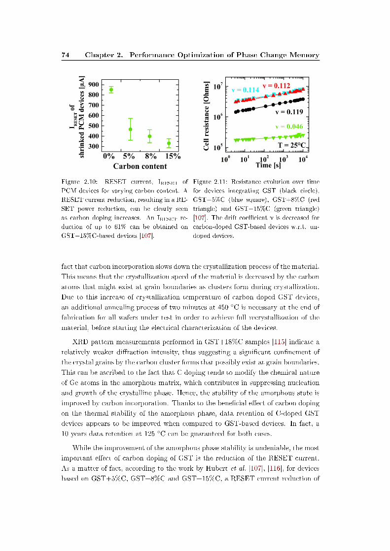
74 Chapter 2. Performance Optimization of Phase Change Memory
Figure 2.10: RESET current, IRESET of
PCM devices for varying carbon content. A
RESET current reduction, resulting in a RE-
SET power reduction, can be clearly seen
as carbon doping increases. An IRESET re-
duction of up to 61% can be obtained on
GST+15%C-based devices [107].
Figure 2.11: Resistance evolution over time
for devices integrating GST (black circle),
GST+5%C (blue square), GST+8%C (red
triangle) and GST+15%C (green triangle)
[107]. The drift coecient ν is decreased for
carbon-doped GST-based devices w.r.t. un-
doped devices.
fact that carbon incorporation slows down the crystallization process of the material.
This means that the crystallization speed of the material is decreased by the carbon
atoms that might exist at grain boundaries as clusters form during crystallization.
Due to this increase of crystallization temperature of carbon doped GST devices,
an additional annealing process of two minutes at 450 C is necessary at the end of
fabrication for all wafers under test in order to achieve full recrystallization of the
material, before starting the electrical characterization of the devices.
XRD pattern measurements performed in GST+18%C samples [115] indicate a
relatively weaker diraction intensity, thus suggesting a signicant connement of
the crystal grains by the carbon cluster forms that possibly exist at grain boundaries.
This can be ascribed to the fact that C doping tends to modify the chemical nature
of Ge atoms in the amorphous matrix, which contributes in suppressing nucleation
and growth of the crystalline phase. Hence, the stability of the amorphous state is
improved by carbon incorporation. Thanks to the benecial eect of carbon doping
on the thermal stability of the amorphous phase, data retention of C-doped GST
devices appears to be improved when compared to GST-based devices. In fact, a
10 years data retention at 125 C can be guaranteed for both cases.
While the improvement of the amorphous phase stability is undeniable, the most
important eect of carbon doping of GST is the reduction of the RESET current.
As a matter of fact, according to the work by Hubert et al. [107], [116], for devices
based on GST+5%C, GST+8%C and GST+15%C, a RESET current reduction of
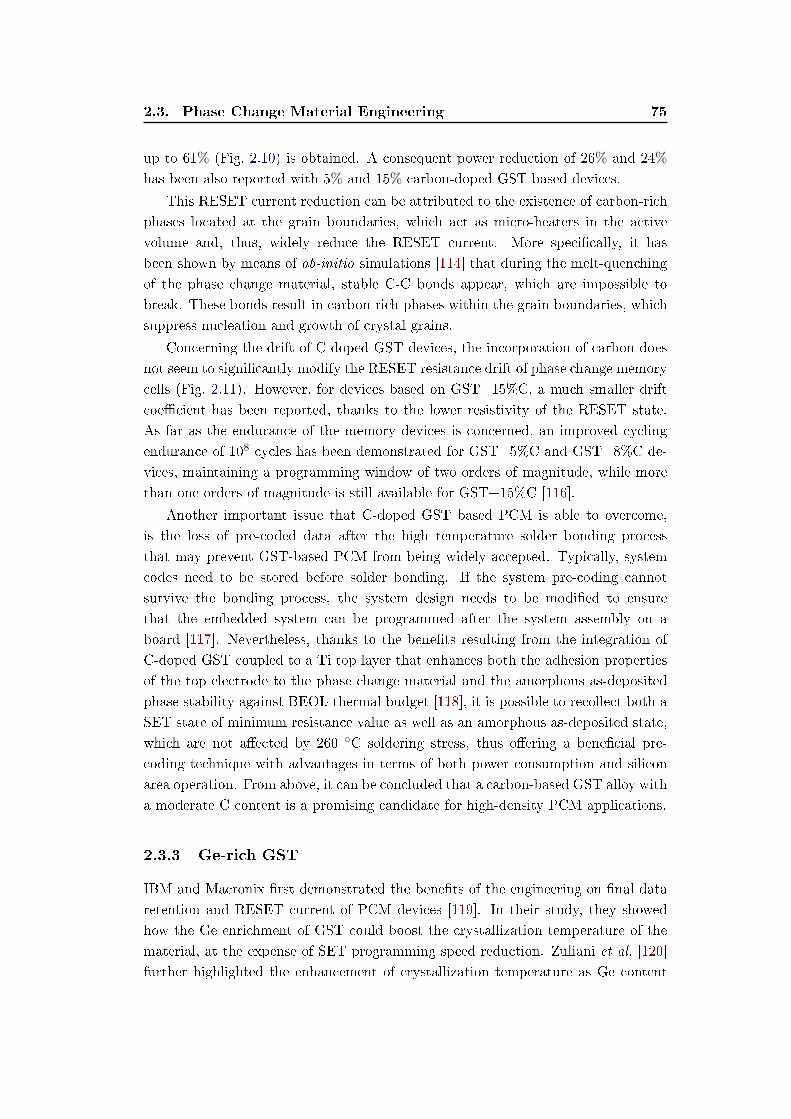
2.3. Phase Change Material Engineering 75
up to 61% (Fig. 2.10) is obtained. A consequent power reduction of 26% and 24%
has been also reported with 5% and 15% carbon-doped GST based devices.
This RESET current reduction can be attributed to the existence of carbon-rich
phases located at the grain boundaries, which act as micro-heaters in the active
volume and, thus, widely reduce the RESET current. More specically, it has
been shown by means of ab-initio simulations [114] that during the melt-quenching
of the phase change material, stable C-C bonds appear, which are impossible to
break. These bonds result in carbon-rich phases within the grain boundaries, which
suppress nucleation and growth of crystal grains.
Concerning the drift of C-doped GST devices, the incorporation of carbon does
not seem to signicantly modify the RESET resistance drift of phase change memory
cells (Fig. 2.11). However, for devices based on GST+15%C, a much smaller drift
coecient has been reported, thanks to the lower resistivity of the RESET state.
As far as the endurance of the memory devices is concerned, an improved cycling
endurance of 108 cycles has been demonstrated for GST+5%C and GST+8%C de-
vices, maintaining a programming window of two orders of magnitude, while more
than one orders of magnitude is still available for GST+15%C [116].
Another important issue that C-doped GST based PCM is able to overcome,
is the loss of pre-coded data after the high temperature solder bonding process
that may prevent GST-based PCM from being widely accepted. Typically, system
codes need to be stored before solder bonding. If the system pre-coding cannot
survive the bonding process, the system design needs to be modied to ensure
that the embedded system can be programmed after the system assembly on a
board [117]. Nevertheless, thanks to the benets resulting from the integration of
C-doped GST coupled to a Ti top layer that enhances both the adhesion properties
of the top electrode to the phase change material and the amorphous as-deposited
phase stability against BEOL thermal budget [118], it is possible to recollect both a
SET state of minimum resistance value as well as an amorphous as-deposited state,
which are not aected by 260 C soldering stress, thus oering a benecial pre-
coding technique with advantages in terms of both power consumption and silicon
area operation. From above, it can be concluded that a carbon-based GST alloy with
a moderate C content is a promising candidate for high-density PCM applications.
2.3.3 Ge-rich GST
IBM and Macronix rst demonstrated the benets of the engineering on nal data
retention and RESET current of PCM devices [119]. In their study, they showed
how the Ge enrichment of GST could boost the crystallization temperature of the
material, at the expense of SET programming speed reduction. Zuliani et al. [120]
further highlighted the enhancement of crystallization temperature as Ge content
76 Chapter 2. Performance Optimization of Phase Change Memory
Figure 2.12: Crystallization temperature of
GST as function of Ge concentration. In-
creasing the Ge content, the crystallization
temperature is enhanced [120].
Figure 2.13: RESET distributions before (t
= 0) and after soldering reow thermal treat-
ment (260 C for 40 s) for an optimized Ge-
rich GST alloy (T-alloy) and an intermediate
D-alloy [120].
increases (Fig. 2.12) and were able to dene an optimized Ge-rich T-alloy, that
proved to be very robust to a soldering reow temperature peak (Fig. 2.13).
The phenomenon of the drift of the RESET phase has also been analyzed in
Ge-rich GST [121]. One of the basic hypotheses made to explain the drift of the
RESET state is that the multiple coordination of Ge atoms in the matrix (tetrahe-
dral bonds of 90 and octahedral bonds of 110) can create a new energy gap state,
thus increasing the structural relaxation process, which is the main cause of the
increased resistance drift observed for the RESET state. As a matter of fact, it has
been shown that mobile atoms lead to very small change in gap states whereas a
nite atomic rearrangement of a local structure results in a bigger gap state change
and, hence, becomes the dominating factor for drift. This is the case in Ge-rich
samples, where the higher the number of possible gap states, the higher the drift
due to the larger structural relaxation.
In order to study and understand the behavior of Ge-rich GST devices, we
performed a series of electrical measurements on Ge-rich GST, integrated in shrunk
Wall structures, while also being interested in the eects of nitrogen and carbon
doping on the nal performance of the devices. We characterized the cells and
started to observe a strong drift also of the SET state, even in samples programmed
with really long pulse-sequences (in the order of tens of µs).
The drift of the RESET state is not detrimental in an industrial memory device,
since it enlarges the resistance window. Nevertheless, a drift of the SET state
towards higher resistance values can be detrimental, as it decreases the resistance
window of the cell, degenerating the information stored in the device and can also
be a major hurdle for the Multilevel Cell potential of PCM technology. In this
light, we report in the following paragraphs a detailed characterization of N- or
2.4. Experimental results 77
C-doped and undoped Ge-rich GST based materials, integrated in state-of-the-art
PCM devices, focusing on the phenomenon of the SET state drift and its eects on
memory performance.
2.4 Experimental results
In order to study the electrical performance of our innovative materials, we inte-
grated N or C-doped and undoped Ge-rich GST materials in state-of-the-art Wall"
structure PCM cells [75], designed specically to perform our analytical studies
on the behavior of dierent materials. The wall thickness is 5 nm while the wall
width varies (depending on the device considered) from a minimum of 60 nm up to
240 nm. The plug is based on a particular titanium nitride alloy, designed to provide
the maximum temperature peak at the plug/phase change material interface. The
deposition process was realized through co-sputtering of one target of Ge2Sb2Te5and one target of Ge and either an additional target of C or under N ux. The
nominal Ge content as referred to in this work varies from 25% up to 45% and the
nominal C and N atomic percentages are 1% and 4%, respectively.
The BEOL temperature was 400 C: all wafers were annealed at this temperature
at the end of the fabrication process ow for two minutes to guarantee full recrys-
tallization before beginning the testing procedure. In order to prepare the devices
for the electrical characterization, we performed a pre-seasoning, consisting of ve
Staircase Up (SCU) and Staircase Down (SCD) sequences, each one (both SCU and
SCD) composed by a series of 50 pulses of increasing (or decreasing) voltage. The
pulse width used was 300 ns, with a rise and fall time of 5 ns.
The SET-RESET characteristics in Fig. 2.14 demonstrate a decrease in the RE-
SET current (by an amount of up to 33%) as the Ge atomic content is increased.
The SET state resistance also appears increased while, at the same time, a smoother
transition slope from the SET to the RESET state can be observed.
The reduction in the RESET current is most likely due to the lower thermal
conductivity of Ge-rich GST with respect to GST. The presence of dierent phases
in the crystalline matrix of the material increases the number of boundaries in the
system, thus leading to an increase of the nal thermal conductivity of the material.
This enables the amorphization of the phase change material at lower currents (lower
temperatures) thanks to the increased thermal eciency of the cell.
The reason why the transition between the SET and the RESET state is smoother
in Ge-rich GST is the lower recrystallization speed of the material, which will be
analyzed in depth later. Even though the pulse amplitude is sucient to melt a
part of the phase change material, the melted volume can be partially recrystallized
during the fall time of the pulse, if the material has a suciently high crystallization
speed (like in the case of GST). In order to obtain a considerable increase of the cell
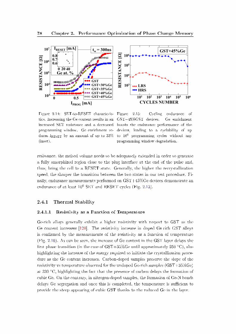
78 Chapter 2. Performance Optimization of Phase Change Memory
0 0.5 1.0
105
IPROG [mA]
RE
SIS
TA
NC
E [Ω
]
tw = 300ns
104
103
106
107
GSTGST+30%Ge
GST+35%Ge
GST+40%GeGST+45%Ge
0 20 40
0.60.70.8
Ge at. %
IRESET [mA]107
Figure 2.14: SET-to-RESET characteris-
tics. Increasing the Ge content results in an
increased SET resistance and a decreased
programming window. Ge enrichment re-
duces IRESET by an amount of up to 33%
(inset).
106
CYCLES NUMBER
RE
SIS
TA
NC
E [Ω
]
LRS
HRS
GST+45%Ge
105
104
103
101 102 103 104 105 106
Figure 2.15: Cycling endurance of
GST+45%GST devices. Ge enrichment
boosts the endurance performance of the
devices, leading to a cyclability of up
to 106 programming cycles without any
programming window degradation.
resistance, the melted volume needs to be adequately extended in order to generate
a fully amorphized region close to the plug interface at the end of the pulse and,
thus, bring the cell to a RESET state. Generally, the higher the recrystallization
speed, the sharper the transition between the two states in our test procedure. Fi-
nally, endurance measurements performed on GST+45%Ge devices demonstrate an
endurance of at least 106 SET and RESET cycles (Fig. 2.15).
2.4.1 Thermal Stability
2.4.1.1 Resistivity as a Function of Temperature
Ge-rich alloys generally exhibit a higher resistivity with respect to GST as the
Ge content increases [120]. The resistivity increase in doped Ge-rich GST alloys
is conrmed by the measurements of the resistivity as a function of temperature
(Fig. 2.16). As can be seen, the increase of Ge content in the GST layer delays the
rst phase transition (in the case of GST+35%Ge until approximately 250 C), also
highlighting the increase of the energy required to initiate the crystallization proce-
dure as the Ge content increases. Carbon-doped samples preserve the slope of the
resistivity vs temperature observed for the undoped Ge-rich samples (GST+35%Ge)
at 330 C, highlighting the fact that the presence of carbon delays the formation of
cubic Ge. On the contrary, in nitrogen-doped samples, the formation of Ge-N bonds
delays Ge segregation and once this is completed, the temperature is sucient to
provide the steep appearing of cubic GST thanks to the reduced Ge in the layer.
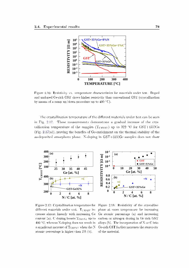
2.4. Experimental results 79
TEMPERATURE [°C]
RE
SIS
TIV
ITY
[Ω
m]
0 100 200 300 400
GSTGST+35%Ge
GST+35%Ge+8%N
GST+35%Ge+1%C
10-3
10-2
10-1
100
102
101
103
104
105
Figure 2.16: Resistivity vs. temperature characteristics for materials under test. Doped
and undoped Ge-rich GST shows higher resistivity than conventional GST (crystallization
by means of a ramp up/down procedure up to 400 C).
The crystallization temperature of the dierent materials under test can be seen
in Fig. 2.17. These measurements demonstrate a gradual increase of the crys-
tallization temperature of the samples (TCRYST) up to 322 C for GST+45%Ge
(Fig. 2.17(a)), proving the benets of Ge-enrichment on the thermal stability of the
as-deposited amorphous phase. N-doping in GST+35%Ge samples does not show
Ge [at. %]
0 2 4 6 8
N / C [at. %]
TC
RY
ST
[°C
]
25 30 35 40 45100
200
300
400(a)
200
300
400
GST-Ge35%
+N
+C(b)
Figure 2.17: Crystallization temperature for
dierent materials under test. TCRYST in-
creases almost linearly with increasing Ge
content (a). C-doping boosts TCRYST up to
400 C, whereas N-doping does not result in
a signicant increase of TCRYST when the N
atomic percentage is higher than 2% (b).
Ge [at. %]
N / C [at. %]
0
0.2
0.4
0.6
0 2 4 6 8
GST+35%Ge
+N+C
(b)
10 20 30 400
GST
GST+X%Ge
(a)10-2
10-1
RE
SIS
TIV
ITY
[Ω
m]
50
10-3
10-4
0.8
Figure 2.18: Resistivity of the crystalline
phase at room temperature for increasing
Ge atomic percentage (a) and increasing
carbon or nitrogen doping in Ge-rich GST
alloys (b). The incorporation of N or C into
Ge-rich GST further increases the resistivity
of the material.
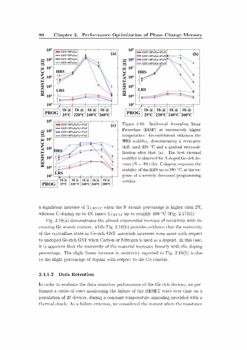
80 Chapter 2. Performance Optimization of Phase Change Memory
103
RE
SIS
TA
NC
E [Ω
]
1h @
25°C
1h @
220°C
1h @
240°C
1h @
260°CPROG
GST+30%Ge
GST+35%Ge
GST+40%Ge
GST+45%Ge
LRS
HRS
(a)
105
106
107
108
104
109
103
RE
SIS
TA
NC
E [Ω
]
1h @
25°C
1h @
220°C
1h @
240°C
1h @
260°CPROG
105
106
107
108
104
109
GST+30%Ge+4%N
GST+35%Ge+4%N
GST+40%Ge+4%N
GST+45%Ge+4%N
LRS
HRS
(b)
LRS
HRS
103
RE
SIS
TA
NC
E [Ω
]
1h @
25°C
1h @
220 °C
1h @
240°C
1h @
260°CPROG
105
106
107
108
104
109
(c)
1h @
280°C
GST+30%Ge%+1%C
GST+35%Ge%+1%C
GST+40%Ge%+1%C
GST+45%Ge%+1%C
Figure 2.19: Isochronal Annealing Steps
Procedure (IASP) at successively higher
temperature. Ge-enrichment enhances the
HRS stability, demonstrating a resistance
drift until 220 C and a gradual recrystal-
lization after that (a). The best thermal
stability is observed for N-doped Ge-rich de-
vices (N = 4%) (b). C-doping improves the
stability of the HRS up to 280 C, at the ex-
pense of a severely decreased programming
window.
a signicant increase of TCRYST when the N atomic percentage is higher than 2%,
whereas C-doping up to 4% raises TCRYST up to roughly 400 C (Fig. 2.17(b)).
Fig. 2.18(a) demonstrates the almost exponential increase of resistivity with in-
creasing Ge atomic content, while Fig. 2.18(b) provides evidence that the resistivity
of the crystalline state in Ge-rich GST materials increases even more with respect
to undoped Ge-rich GST when Carbon or Nitrogen is used as a dopant. In this case,
it is apparent that the resistivity of the material increases linearly with the doping
percentage. The slight linear increase in resistivity reported in Fig. 2.18(b) is due
to the slight percentage of dopant with respect to the Ge content.
2.4.1.2 Data Retention
In order to evaluate the data retention performance of the Ge-rich devices, we per-
formed a series of tests monitoring the failure of the RESET state over time on a
population of 20 devices, during a constant temperature annealing provided with a
thermal chuck. As a failure criterion, we considered the instant when the resistance
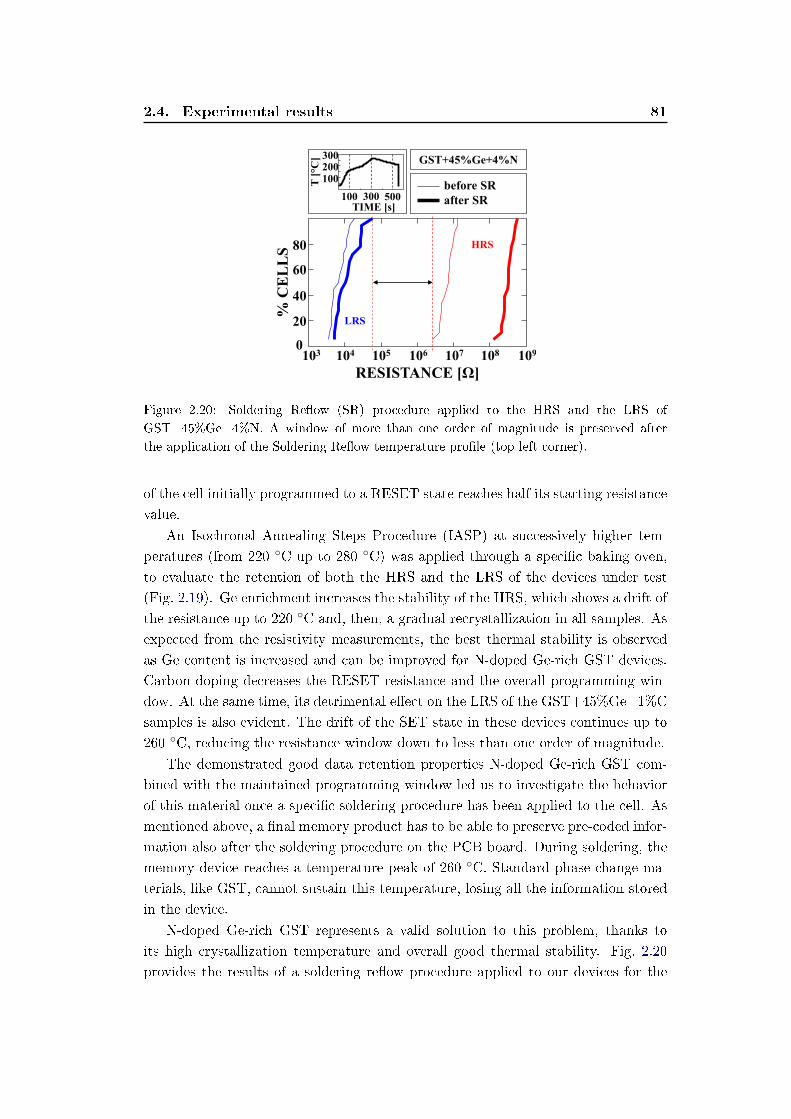
2.4. Experimental results 81
LRS
HRS
GST+45%Ge+4%N
before SR
after SR
103
RESISTANCE [Ω]
40
60
80
% C
EL
LS
TIME [s]100 300 500
100200300
T [
°C]
104 105 106 107 108 109
20
0
Figure 2.20: Soldering Reow (SR) procedure applied to the HRS and the LRS of
GST+45%Ge+4%N. A window of more than one order of magnitude is preserved after
the application of the Soldering Reow temperature prole (top left corner).
of the cell initially programmed to a RESET state reaches half its starting resistance
value.
An Isochronal Annealing Steps Procedure (IASP) at successively higher tem-
peratures (from 220 C up to 280 C) was applied through a specic baking oven,
to evaluate the retention of both the HRS and the LRS of the devices under test
(Fig. 2.19). Ge enrichment increases the stability of the HRS, which shows a drift of
the resistance up to 220 C and, then, a gradual recrystallization in all samples. As
expected from the resistivity measurements, the best thermal stability is observed
as Ge content is increased and can be improved for N-doped Ge-rich GST devices.
Carbon doping decreases the RESET resistance and the overall programming win-
dow. At the same time, its detrimental eect on the LRS of the GST+45%Ge+1%C
samples is also evident. The drift of the SET state in these devices continues up to
260 C, reducing the resistance window down to less than one order of magnitude.
The demonstrated good data retention properties N-doped Ge-rich GST com-
bined with the maintained programming window led us to investigate the behavior
of this material once a specic soldering procedure has been applied to the cell. As
mentioned above, a nal memory product has to be able to preserve pre-coded infor-
mation also after the soldering procedure on the PCB board. During soldering, the
memory device reaches a temperature peak of 260 C. Standard phase change ma-
terials, like GST, cannot sustain this temperature, losing all the information stored
in the device.
N-doped Ge-rich GST represents a valid solution to this problem, thanks to
its high crystallization temperature and overall good thermal stability. Fig. 2.20
provides the results of a soldering reow procedure applied to our devices for the
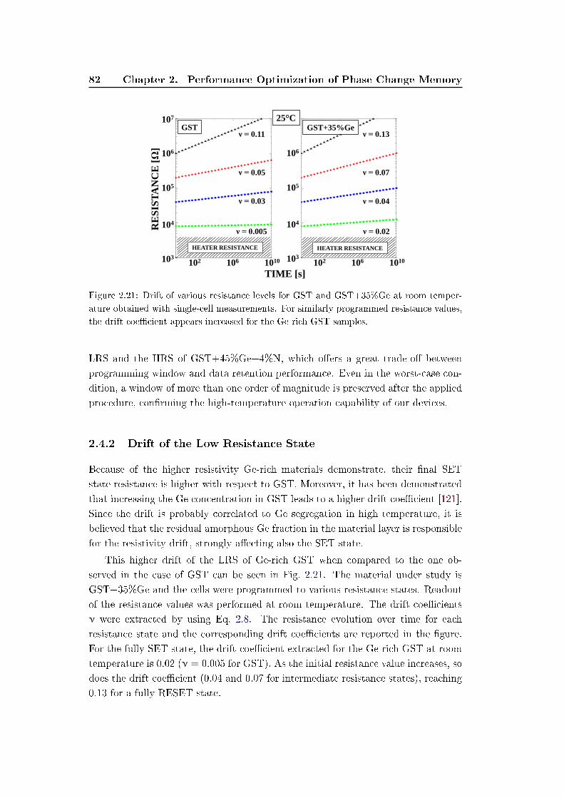
82 Chapter 2. Performance Optimization of Phase Change Memory
100
102
104
106
108
1010
103
104
105
106
107
100
102
104
106
108
1010
103
104
105
106
107
GST+35%Ge107
106
105
104
103
107
106
105
104
103102 106 1010 102 106 1010
GST
TIME [s]
RE
SIS
TA
NC
E [
Ω]
HEATER RESISTANCE HEATER RESISTANCE
ν = 0.11
ν = 0.005
ν = 0.05
ν = 0.03
ν = 0.13
ν = 0.07
ν = 0.04
ν = 0.02
25°C
Figure 2.21: Drift of various resistance levels for GST and GST+35%Ge at room temper-
ature obtained with single-cell measurements. For similarly programmed resistance values,
the drift coecient appears increased for the Ge-rich GST samples.
LRS and the HRS of GST+45%Ge+4%N, which oers a great trade-o between
programming window and data retention performance. Even in the worst-case con-
dition, a window of more than one order of magnitude is preserved after the applied
procedure, conrming the high-temperature operation capability of our devices.
2.4.2 Drift of the Low Resistance State
Because of the higher resistivity Ge-rich materials demonstrate, their nal SET
state resistance is higher with respect to GST. Moreover, it has been demonstrated
that increasing the Ge concentration in GST leads to a higher drift coecient [121].
Since the drift is probably correlated to Ge segregation in high temperature, it is
believed that the residual amorphous Ge fraction in the material layer is responsible
for the resistivity drift, strongly aecting also the SET state.
This higher drift of the LRS of Ge-rich GST when compared to the one ob-
served in the case of GST can be seen in Fig. 2.21. The material under study is
GST+35%Ge and the cells were programmed to various resistance states. Readout
of the resistance values was performed at room temperature. The drift coecients
ν were extracted by using Eq. 2.8. The resistance evolution over time for each
resistance state and the corresponding drift coecients are reported in the gure.
For the fully SET state, the drift coecient extracted for the Ge-rich GST at room
temperature is 0.02 (ν = 0.005 for GST). As the initial resistance value increases, so
does the drift coecient (0.04 and 0.07 for intermediate resistance states), reaching
0.13 for a fully RESET state.
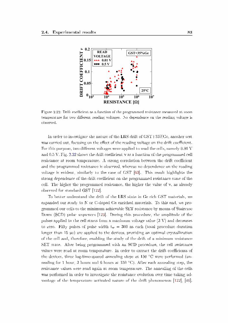
2.4. Experimental results 83
103 104 105 1070
0.05
0.1
0.15
0.2
RESISTANCE [Ω]
DR
IFT
CO
EF
FIC
IEN
T v
GST+35%Ge
25°C
0.01 V0.5 V
READ
VOLTAGE
106
Figure 2.22: Drift coecient as a function of the programmed resistance measured at room
temperature for two dierent reading voltages. No dependence on the reading voltage is
observed.
In order to investigate the nature of the LRS drift of GST+35%Ge, another test
was carried out, focusing on the eect of the reading voltage on the drift coecient.
For this purpose, two dierent voltages were applied to read the cells, namely 0.01 V
and 0.5 V. Fig. 2.22 shows the drift coecient ν as a function of the programmed cell
resistance at room temperature. A strong correlation between the drift coecient
and the programmed resistance is observed, whereas no dependence on the reading
voltage is evident, similarly to the case of GST [63]. This result highlights the
strong dependence of the drift coecient on the programmed resistance state of the
cell. The higher the programmed resistance, the higher the value of ν, as already
observed for standard GST [122].
To better understand the drift of the LRS state in Ge-rich GST materials, we
expanded our study to N or C-doped Ge enriched materials. To this end, we pro-
grammed our cells to the minimum achievable SET resistance by means of Staircase
Down (SCD) pulse sequences [123]. During this procedure, the amplitude of the
pulses applied to the cell starts from a maximum voltage value (3 V) and decreases
to zero. Fifty pulses of pulse width tw = 300 ns each (total procedure duration
longer than 15 µs) are applied to the devices, providing an optimal crystallization
of the cell and, therefore, enabling the study of the drift of a minimum resistance
SET state. After being programmed with an SCD procedure, the cell resistance
values were read at room temperature. In order to extract the drift coecients of
the devices, three log-time-spaced annealing steps at 150 C were performed (an-
nealing for 1 hour, 3 hours and 6 hours at 150 C). After each annealing step, the
resistance values were read again at room temperature. The annealing of the cells
was performed in order to investigate the resistance evolution over time taking ad-
vantage of the temperature activated nature of the drift phenomenon [122], [46].
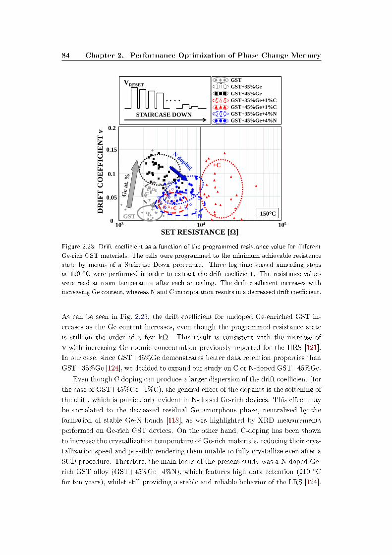
84 Chapter 2. Performance Optimization of Phase Change Memory
150°C
+C
+N GST
GST
GST+35%Ge
GST+45%Ge
GST+35%Ge+1%C
GST+45%Ge+1%C
GST+35%Ge+4%N
GST+45%Ge+4%N
103 104 105 0
0.05
0.1
0.15
SET RESISTANCE [Ω]
DR
IFT
CO
EF
FIC
IEN
T v
+C
0.2
STAIRCASE DOWN
VRESET
Figure 2.23: Drift coecient as a function of the programmed resistance value for dierent
Ge-rich GST materials. The cells were programmed to the minimum achievable resistance
state by means of a Staircase Down procedure. Three log-time-spaced annealing steps
at 150 C were performed in order to extract the drift coecient. The resistance values
were read at room temperature after each annealing. The drift coecient increases with
increasing Ge content, whereas N and C incorporation results in a decreased drift coecient.
As can be seen in Fig. 2.23, the drift coecient for undoped Ge-enriched GST in-
creases as the Ge content increases, even though the programmed resistance state
is still on the order of a few kΩ. This result is consistent with the increase of
ν with increasing Ge atomic concentration previously reported for the HRS [121].
In our case, since GST+45%Ge demonstrates better data retention properties than
GST+35%Ge [124], we decided to expand our study on C or N-doped GST+45%Ge.
Even though C doping can produce a larger dispersion of the drift coecient (for
the case of GST+45%Ge+1%C), the general eect of the dopants is the softening of
the drift, which is particularly evident in N-doped Ge-rich devices. This eect may
be correlated to the decreased residual Ge amorphous phase, neutralised by the
formation of stable Ge-N bonds [118], as was highlighted by XRD measurements
performed on Ge-rich GST devices. On the other hand, C-doping has been shown
to increase the crystallization temperature of Ge-rich materials, reducing their crys-
tallization speed and possibly rendering them unable to fully crystallize even after a
SCD procedure. Therefore, the main focus of the present study was a N-doped Ge-
rich GST alloy (GST+45%Ge+4%N), which features high data retention (210 C
for ten years), whilst still providing a stable and reliable behavior of the LRS [124].
2.4. Experimental results 85
The positive eect of N-doped Ge-rich GST on the LRS drift, reported in Fig. 2.23,
is a conclusion reached based on drift coecients extracted after programming the
cell with a time consuming SCD sequence, which ensures that a minimum-resistance
SET state is achieved. However, in order to be able to address nal applications, this
good result in terms of LRS drift has to be achieved with a reduced programming
time. An investigation aimed at this purpose is provided in the following.
2.4.3 Crystallization Speed
In order to program a PCM device to the SET and the RESET state, specic
currents are required. For the RESET state, the required current has to be able to
provide a temperature prole adequate to rst induce melting and then rapidly cool
the phase change material, whereas the SET current has to be lower but still large
enough to enable the crystallization of the cell [44]. The SET operation determines
the write speed performance of PCM technology, since it is much slower than the
RESET operation [108]. The required duration of the SET pulse depends on the
crystallization speed of the phase change material.
Crystallization speed is probably the most critical property of PCM because it
sets an upper limit on the potential write data rate of the technology. In order
to characterize the crystallization speed of our devices, we performed a series of
recrystallization cartographies (Fig. 2.24). The cells were initially prepared in the
RESET state and, then, single programming pulses with increasing amplitude were
applied. The cartographies reported in Fig. 2.24(a) were obtained by reading the
resistance value after applying a single programming pulse. The pulse fall time tfwas xed at a constant value (5 ns) whereas the pulse width tw was increased. In
Fig. 2.24(b), a similar procedure was followed but, in this case, the width of the
SET pulse was kept constant (300 ns), whereas dierent values of pulse fall time tfwere used. In both cases, the delay between the RESET and the SET pulse was on
the order of hundreds of ns.
Fig. 2.24 demonstrates the reduction of the SET speed of Ge-rich samples with
respect to the case of GST devices. As far as the increase of SET pulse width is
concerned (Fig. 2.24(a)), although GST easily crystallizes for a SET pulse width
of 100 ns (tf = 5 ns), this does not seem to be the case for the Ge-rich GST and
the N-doped Ge-rich GST, where the SET state can be achieved by means of a
pulse with tw = 200 ns. For the C-doped Ge-rich material, crystallization speed is
even lower: a pulse of 400 ns is required to bring the cell to the LRS. Moreover,
the resistance programming window in this case appears to be decreased to almost
merely one order of magnitude, which is substantially narrower than in the case
of undoped and N-doped Ge-rich devices. This result suggests that a single SET
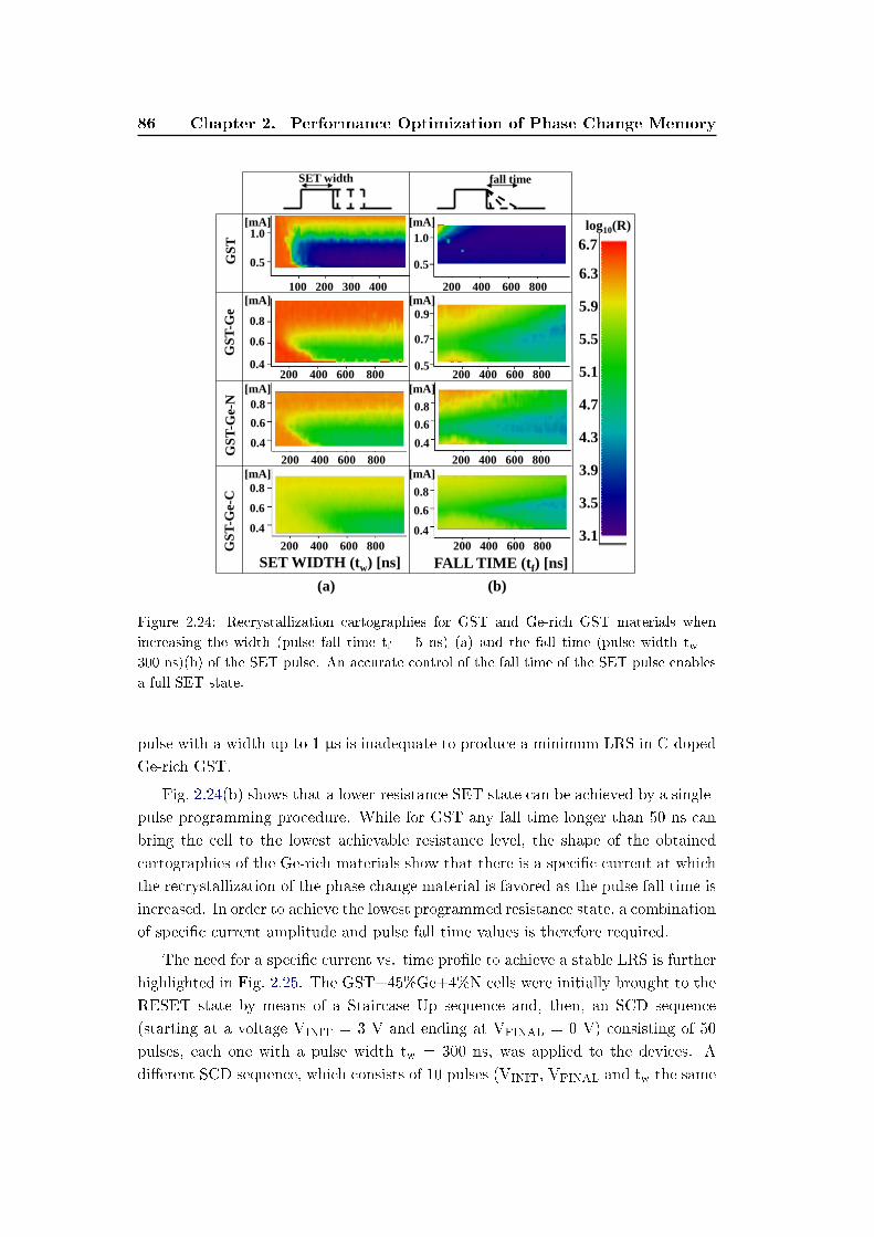
86 Chapter 2. Performance Optimization of Phase Change Memory
GS
T-G
e-N
G
ST
-Ge-
C
log10(R)
SET WIDTH (tw) [ns] FALL TIME (tf) [ns]
SET width fall time
6.7
6.3
5.9
5.5
5.1
4.7
4.3
3.9
3.5
3.1
1.0
0.5
100 200 300 400
1.0
0.5
200 400 600 800
0.8
0.6 0.4
0.9
0.7
0.5 200 400 600 800
0.8 0.6 0.4
0.8 0.6 0.4
0.8 0.6 0.4
0.8 0.6 0.4
[mA] [mA]
[mA] [mA]
[mA]
[mA] [mA]
[mA]
GS
T-G
e G
ST
200 400 600 800
200 400 600 800
200 400 600 800
200 400 600 800
200 400 600 800
(a) (b)
Figure 2.24: Recrystallization cartographies for GST and Ge-rich GST materials when
increasing the width (pulse fall time tf = 5 ns) (a) and the fall time (pulse width tw =
300 ns)(b) of the SET pulse. An accurate control of the fall time of the SET pulse enables
a full SET state.
pulse with a width up to 1 µs is inadequate to produce a minimum LRS in C-doped
Ge-rich GST.
Fig. 2.24(b) shows that a lower-resistance SET state can be achieved by a single-
pulse programming procedure. While for GST any fall time longer than 50 ns can
bring the cell to the lowest achievable resistance level, the shape of the obtained
cartographies of the Ge-rich materials show that there is a specic current at which
the recrystallization of the phase change material is favored as the pulse fall time is
increased. In order to achieve the lowest programmed resistance state, a combination
of specic current amplitude and pulse fall time values is therefore required.
The need for a specic current vs. time prole to achieve a stable LRS is further
highlighted in Fig. 2.25. The GST+45%Ge+4%N cells were initially brought to the
RESET state by means of a Staircase Up sequence and, then, an SCD sequence
(starting at a voltage VINIT = 3 V and ending at VFINAL = 0 V) consisting of 50
pulses, each one with a pulse width tw = 300 ns, was applied to the devices. A
dierent SCD sequence, which consists of 10 pulses (VINIT, VFINAL and tw the same
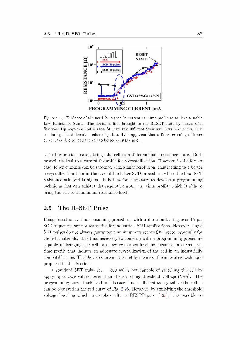
2.5. The RSET Pulse 87
0 0.5 1104
105
106
107
PROGRAMMING CURRENT [mA]
RE
SIS
TA
NC
E [Ω
]
RESET
STATE
GST+45%Ge+4%N
...
SCU
SCD (50 pulses)
SCD (10 pulses)
Figure 2.25: Evidence of the need for a specic current vs. time prole to achieve a stable
Low Resistance State. The device is rst brought to the RESET state by means of a
Staircase Up sequence and is then SET by two dierent Staircase Down sequences, each
consisting of a dierent number of pulses. It is apparent that a ner screening of lower
currents is able to lead the cell to better crystallization.
as in the previous case), brings the cell to a dierent nal resistance state. Both
procedures lead to a current favorable for recrystallization. However, in the former
case, lower currents can be screened with a ner resolution, thus leading to a better
recrystallization than in the case of the latter SCD procedure, where the nal SET
resistance achieved is higher. It is therefore necessary to develop a programming
technique that can achieve the required current vs. time prole, which is able to
bring the cell to a minimum resistance level.
2.5 The RSET Pulse
Being based on a time-consuming procedure, with a duration lasting over 15 µs,
SCD sequences are not attractive for industrial PCM applications. However, single
SET pulses do not always guarantee a minimum-resistance SET state, especially for
Ge-rich materials. It is thus necessary to come up with a programming procedure
capable of bringing the cell to a low resistance level by means of a current vs.
time prole that induces an adequate crystallization of the cell in an industrially
compatible time. The above requirement is met by means of the innovative technique
proposed in this Section.
A standard SET pulse (tw = 300 ns) is not capable of switching the cell by
applying voltage values lower than the switching threshold voltage (VTH). The
programming current achieved in this case is not sucient to crystallize the cell as
can be observed in the red curve of Fig. 2.26. However, by exploiting the threshold
voltage lowering which takes place after a RESET pulse [125], it is possible to
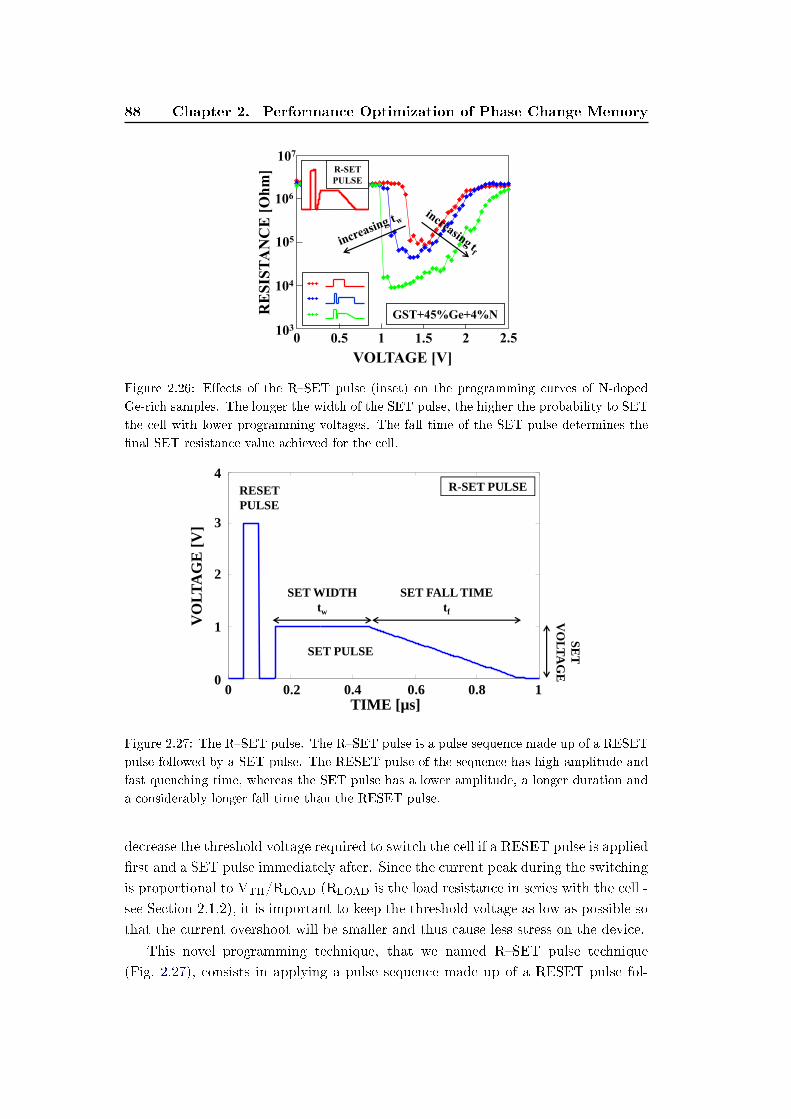
88 Chapter 2. Performance Optimization of Phase Change Memory
0 0.5 1 1.5 2 2.5103
VOLTAGE [V]
RE
SIS
TA
NC
E [
Oh
m]
104
105
106
107
R-SET
PULSE
GST+45%Ge+4%N
Figure 2.26: Eects of the RSET pulse (inset) on the programming curves of N-doped
Ge-rich samples. The longer the width of the SET pulse, the higher the probability to SET
the cell with lower programming voltages. The fall time of the SET pulse determines the
nal SET resistance value achieved for the cell.
0 0.2 0.4 0.6 0.8 1
x 10-6
0
1
2
3
4
SET WIDTHtw
SET FALL TIMEtf
RESET PULSE
SET PULSE
R-SET PULSE
SE
T
VO
LTAG
E
VO
LTA
GE
[V]
1
2
3
4
0 0.2 0.4 0.6 0.8 1TIME [µs]
0
Figure 2.27: The RSET pulse. The RSET pulse is a pulse sequence made up of a RESET
pulse followed by a SET pulse. The RESET pulse of the sequence has high amplitude and
fast quenching time, whereas the SET pulse has a lower amplitude, a longer duration and
a considerably longer fall time than the RESET pulse.
decrease the threshold voltage required to switch the cell if a RESET pulse is applied
rst and a SET pulse immediately after. Since the current peak during the switching
is proportional to VTH/RLOAD (RLOAD is the load resistance in series with the cell -
see Section 2.1.2), it is important to keep the threshold voltage as low as possible so
that the current overshoot will be smaller and thus cause less stress on the device.
This novel programming technique, that we named RSET pulse technique
(Fig. 2.27), consists in applying a pulse sequence made up of a RESET pulse fol-
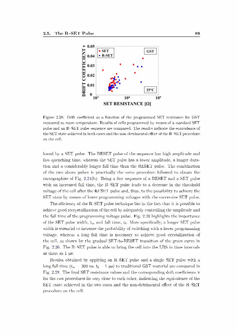
2.5. The RSET Pulse 89
SET RESISTANCE [Ω]
DR
IFT
CO
EFF
ICIE
NT
ν
GST
25°C
103 104 1050
0.01
0.05
0.02
0.04
0.03
SETR-SET
Figure 2.28: Drift coecient as a function of the programmed SET resistance for GST
measured at room temperature. Results of cells programmed by means of a standard SET
pulse and an RSET pulse sequence are compared. The results indicate the equivalence of
the SET state achieved in both cases and the non-detrimental eect of the RSET procedure
on the cell.
lowed by a SET pulse. The RESET pulse of the sequence has high amplitude and
fast quenching time, whereas the SET pulse has a lower amplitude, a longer dura-
tion and a considerably longer fall time than the RESET pulse. The combination
of the two above pulses is practically the same procedure followed to obtain the
cartographies of Fig. 2.24(b). Being a fast sequence of a RESET and a SET pulse
with an increased fall time, the RSET pulse leads to a decrease in the threshold
voltage of the cell after the RESET pulse and, thus, to the possibility to achieve the
SET state by means of lower programming voltages with the successive SET pulse.
The eciency of the RSET pulse technique lies in the fact that it is possible to
achieve good recrystallization of the cell by adequately controlling the amplitude and
the fall time of the programming voltage pulse. Fig. 2.26 highlights the importance
of the SET pulse width, tw and fall time, tf. More specically, a longer SET pulse
width is essential to increase the probability of switching with a lower programming
voltage, whereas a long fall time is necessary to achieve good crystallization of
the cell, as shown by the gradual SET-to-RESET transition of the green curve in
Fig. 2.26. The RSET pulse is able to bring the cell into the LRS in time intervals
as short as 1 µs.
Results obtained by applying an RSET pulse and a single SET pulse with a
long fall time (tw = 300 ns, tf = 1 µs) to traditional GST material are compared in
Fig. 2.28. The nal SET resistance values and the corresponding drift coecients ν
for the two procedures lie very close to each other, indicating the equivalence of the
SET state achieved in the two cases and the non-detrimental eect of the RSET
procedure on the cell.
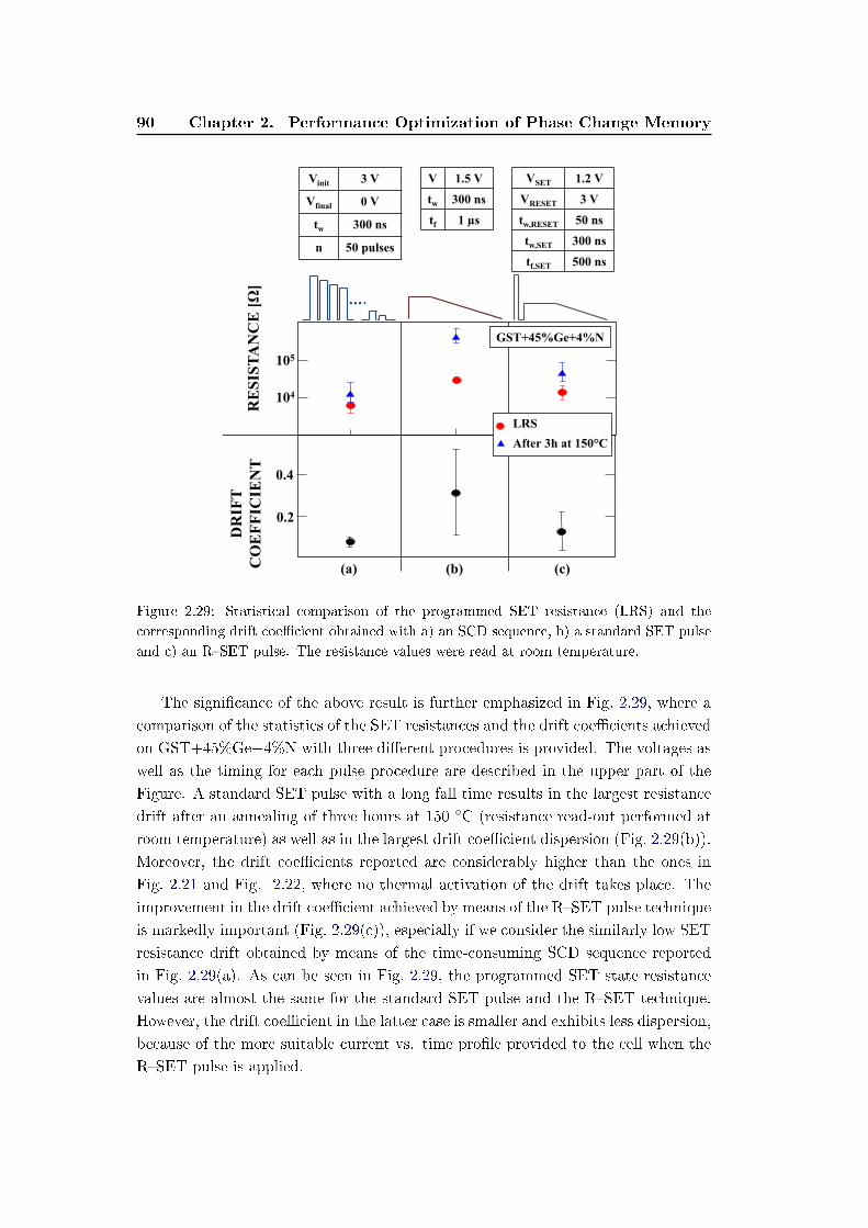
90 Chapter 2. Performance Optimization of Phase Change Memory
104
105
RE
SIS
TA
NC
E [Ω
]
0.2
0.4
DR
IFT
CO
EF
FIC
IEN
T
GST+45%Ge+4%N
(a) (b) (c)
LRS
After 3h at 150°C
Vinit 3 V
Vfinal 0 V
tw 300 ns
n 50 pulses
VSET 1.2 V
VRESET 3 V
tw,RESET 50 ns
tw,SET 300 ns
tf,SET 500 ns
V 1.5 V
tw 300 ns
tf 1 µs
Figure 2.29: Statistical comparison of the programmed SET resistance (LRS) and the
corresponding drift coecient obtained with a) an SCD sequence, b) a standard SET pulse
and c) an RSET pulse. The resistance values were read at room temperature.
The signicance of the above result is further emphasized in Fig. 2.29, where a
comparison of the statistics of the SET resistances and the drift coecients achieved
on GST+45%Ge+4%N with three dierent procedures is provided. The voltages as
well as the timing for each pulse procedure are described in the upper part of the
Figure. A standard SET pulse with a long fall time results in the largest resistance
drift after an annealing of three hours at 150 C (resistance read-out performed at
room temperature) as well as in the largest drift coecient dispersion (Fig. 2.29(b)).
Moreover, the drift coecients reported are considerably higher than the ones in
Fig. 2.21 and Fig. 2.22, where no thermal activation of the drift takes place. The
improvement in the drift coecient achieved by means of the RSET pulse technique
is markedly important (Fig. 2.29(c)), especially if we consider the similarly low SET
resistance drift obtained by means of the time-consuming SCD sequence reported
in Fig. 2.29(a). As can be seen in Fig. 2.29, the programmed SET state resistance
values are almost the same for the standard SET pulse and the RSET technique.
However, the drift coecient in the latter case is smaller and exhibits less dispersion,
because of the more suitable current vs. time prole provided to the cell when the
RSET pulse is applied.
2.6. Summary of the Chapter 91
Even though these innovative materials demonstrate drift coecients higher than
conventional phase change materials such as GST, they still represent a solution
compliant with industrial standards, thanks to their high crystallization temper-
ature. Final memory products have to be capable of preserving pre-coded infor-
mation also after the soldering procedure on the PCB board. It has been shown
that GST+45%Ge+4%N can reach a temperature peak of 260 C without any in-
formation loss. On the contrary, standard phase change materials cannot sustain
such high temperatures, losing all the information stored in the device, therefore
requiring a post-coding procedure, once the memory is already soldered. There-
fore, our materials represent a promising solution to this problem, demonstrating
an exceptional thermal stability of the HRS as well as of the LRS.
2.6 Summary of the Chapter
Phase Change Memory provides an attractive set of features, which is of great
interest for innovative applications, while its ability to match the cost of existing
memory technologies makes PCM technology a promising candidate to enter a well
established memory market.
Phase change material properties are known to aect PCM device parameters
such as the crystallization temperature, data retention and lifetime, while resistivity
values of the amorphous and crystalline phases impact the voltage needed to pro-
gram the cell. Understanding and improving the reliability of these cells becomes
therefore a limiting factor to successful deployment of the technology in reliable
products. Technology improvements can be achieved by optimizing the materials
and the processes used to produce the cells as well as the methods used to program
the cells.
Most of the development has focused on the optimization of the cell architecture
in order to increase programming eciency. However, proper material engineering
enables the reduction of the programming current required for RESET program-
ming. The reliability optimization of PCM devices based on alternative-to-GST
materials is a very promising solution to enhance device performance.
Through a series of extensive electrical characterization, the reliability enhance-
ment thanks to an innovative N-doped Ge-rich chalcogenide material was studied
and the overall excellent thermal stability properties of the material were demon-
strated, conrming the high-temperature operation capability of our devices. A
decreased crystallization speed combined with a residual drift phenomenon in the
SET state was also observed, thus rendering slower the SET programming of mem-
ory devices based on these innovative materials, aecting the memory technology
throughput.
92 Chapter 2. Performance Optimization of Phase Change Memory
Nonetheless, the drift of the LRS of the Ge-rich GST appears to be reduced when
N is co-incorporated into the material. The recrystallization cartographies provided
for the study of the crystallization speed of the considered materials highlight the
need for a specic current versus time prole to achieve a SET state where the LRS
drift is reduced. To obtain the desired current vs. time prole and, at the same
time, reduce the LRS drift, an innovative programming technique named R-SET
technique was introduced.
The R-SET pulse, which is a fast sequence of a RESET and a SET pulse, takes
advantage of the threshold voltage decrease occurring after the application of a
RESET pulse to the cell and results in a low resistance SET state with a drift
coecient comparable with the one obtained by means of time-consuming SCD
procedures. This solution can lead to optimal crystallization and reduced LRS drift
in industrially compatible times, thus making these innovative materials suitable for
embedded applications with stringent requirements on data retention.
Chapter 3
Innovative PCM Circuit Design
In order for PCM to become a viable technology for high-volume manufacturing, its
reliability has to be brought to a level similar to that of existing non-volatile memory
technologies. The low crystallization temperature of GST results in poor thermal
stability and, thus, in limited data retention. Another downside of GST is the high
current required to bring the material to the amorphous phase from the well ordered,
crystalline one. Resistance drift remains one of the most important reliability issues
of this technology, resulting in a resistivity increase of the amorphous phase of
chalcogenide materials over time, thus adversely aecting the multilevel storage
potential of PCM, since stochastic shifts of closely spaced programmed resistance
levels may cause them to overlap and therefore lead to decoding errors [66].
Reliability of PCM can be optimized by innovative materials, such as Ge-rich
GST. While Ge enrichment has a positive impact on PCM performance [119], it
also leads to an increase in the resistivity of the crystalline state and a subsequent
SET state resistivity drift. Suppression of this phenomenon can be achieved if the
cell is optimally crystallized and brought to a minimum resistance level by means
of a pulse sequence of decreasing amplitude, referred to as Staircase Down (SCD)
programming [123], which is generally considered as a long procedure, incapable of
crystallizing the cell in industrially compatible times. Therefore, new programming
techniques must be utilized in order to guarantee reliable programming of memory
devices, yet remaining compliant with industrial standards.
To this purpose, new circuit architectures targeting accurate programming of
PCM based on innovative materials have to be discussed. In the rst Section of the
present Chapter, we start with the R-SET pulse, which was introduced previously
and we present a fully tunable pulse generator, capable of providing the desired
pulse waveform. Next, we introduce a programming technique which consists in
providing a voltage pulse that enables a linearly decreasing temperature prole to
the PCM cells. The purpose of this pulse is to optimally activate the growth of the
crystals and thus lead to a SET state of minimum resistance value, where the drift
is possibly suppressed.
Finally, the Chapter concludes with a current pulse generator capable of Multi-
level Cell programming. Taking advantage of the slow crystallization speed Ge-rich
GST materials demonstrate with respect to conventional GST, we show that the
94 Chapter 3. Innovative PCM Circuit Design
presented circuit is capable of programming memory devices to intermediate states
enabling 2-bit-per-cell operation without resistance distribution overlap.
All circuit schematics shown in this Chapter were developed having PCM cell
characterization as the key target. The circuits were designed in 130 nm CMOS
technology, which is a typical fabrication technology for peripheral circuits of non-
volatile memories. All the waveforms provided in the following of the Chapter were
obtained by circuit simulation in Cadence environment using the above technology.
3.1 The R-SET Pulse Generator
As discussed in the previous Chapter, Ge enrichment of GST as well as the intro-
duction of dopants such as C and N result in exceptional data retention properties.
However, in order to cope with the lower crystallization speed of these materials
and, at the same time, be able to crystallize well the PCM cells and reduce the
undesired SET state drift phenomenon, an appropriate current vs. time prole has
to be provided to the cell.
Since the drift dynamics strongly depend on the programmed resistance level [57],
programming a memory cell to a minimum resistance value results in a low drift
coecient. An SCD programming sequence is able to provide a minimum SET state
resistance and a correspondingly low drift coecient. However, for a sequence of
50 pulses of width tw = 300 ns, the total duration of the procedure exceeds 15 µs,
thus rendering the application of the SCD sequence inappropriate for industrial
applications.
Single programming pulses do not always guarantee a minimum resistance SET
state, especially for Ge-rich materials. In this case, a standard SET pulse (with a
duration of tw = 300 ns) is not able to switch the memory cell by applying volt-
ages lower than the switching threshold voltage VTH, and, hence, the programming
current achieved in this case is not sucient to provide crystallization of the active
material of the cell.
Applying a voltage V > VTH with a large load resistance RLOAD in series with 1R
memory cells leads to low current in the ON regime but, at the same time, increases
parasitic contributions, thus limiting the achievable pulse width and not favoring the
study of the material speed. Nevertheless, the threshold voltage required to switch
the cell can be decreased if we take advantage of the threshold voltage lowering
which occurs immediately after the application of a RESET pulse [125]. During
switching, the current peak is proportional to VTH/RLOAD. Keeping the threshold
voltage as low as possible is important in order to minimize the current peak and
thus cause less stress on the device. To this end, a new programming technique,
named R-SET pulse, is proposed.
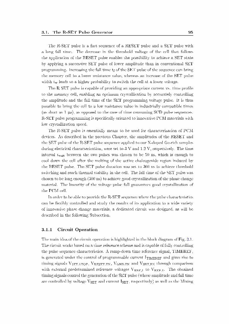
3.1. The R-SET Pulse Generator 95
The R-SET pulse is a fast sequence of a RESET pulse and a SET pulse with
a long fall time. The decrease in the threshold voltage of the cell that follows
the application of the RESET pulse enables the possibility to achieve a SET state
by applying a successive SET pulse of lower amplitude than in conventional SET
programming. Increasing the fall time tf of the SET pulse of the sequence can bring
the memory cell to a lower resistance value, whereas an increase of the SET pulse
width tw leads to a higher probability to switch the cell at a lower voltage.
The R-SET pulse is capable of providing an appropriate current vs. time prole
to the memory cell, enabling an optimum crystallization by accurately controlling
the amplitude and the fall time of the SET programming voltage pulse. It is thus
possible to bring the cell to a low resistance value in industrially compatible times
(as short as 1 µs), as opposed to the case of time-consuming SCD pulse sequences.
R-SET pulse programming is specically oriented to innovative PCM materials with
low crystallization speed.
The R-SET pulse is essentially meant to be used for characterization of PCM
devices. As described in the previous Chapter, the amplitudes of the RESET and
the SET pulse of the R-SET pulse sequence applied to our N-doped Ge-rich samples
during electrical characterization, were set to 3 V and 1.2 V, respectively. The time
interval twait between the two pulses was chosen to be 50 ns, which is enough to
cool down the cell after the melting of the active chalcogenide region induced by
the RESET pulse. The SET pulse duration was set to 300 ns to achieve threshold
switching and reach thermal stability in the cell. The fall time of the SET pulse was
chosen to be long enough (500 ns) to achieve good crystallization of the phase change
material. The linearity of the voltage pulse fall guarantees good crystallization of
the PCM cell.
In order to be able to provide the R-SET sequence where the pulse characteristics
can be exibly controlled and study the results of its application to a wide variety
of innovative phase change materials, a dedicated circuit was designed, as will be
described in the following Subsection.
3.1.1 Circuit Operation
The main idea of the circuit operation is highlighted in the block diagram of Fig. 3.1.
The circuit works based on a time reference scheme and is capable of fully controlling
the pulse sequence characteristics. A ramp-down time reference signal, TIMEREF,
is generated under the control of programmable current ITIMEREF and gives rise to
timing signals VSET,STOP, VRESET,EN, VGND,EN and VSET,EN through comparison
with external predetermined reference voltages VREF,1 to VREF,4. The obtained
timing signals control the generation of the SET pulse (whose amplitude and fall time
are controlled by voltage VSET and current ISET, respectively) as well as the Mixing
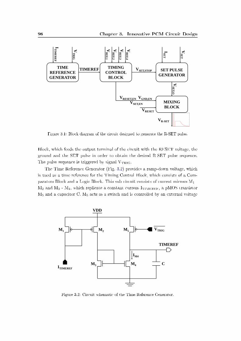
96 Chapter 3. Innovative PCM Circuit Design
TIMEREFTIME REFERENCE GENERATOR
IT
IME
RE
F
VT
RIG
SET PULSE GENERATOR
MIXING BLOCK
ISE
T
VSE
T
VSE
T,O
TIMING CONTROL
BLOCK
VR
EF,2
VR
EF,3
VR
EF,4
VR
EF,1
VSET,STOP
VRESET
VRESET,EN VGND,ENVSET,EN
VR-SET
Figure 3.1: Block diagram of the circuit designed to generate the R-SET pulse.
Block, which feeds the output terminal of the circuit with the RESET voltage, the
ground and the SET pulse in order to obtain the desired R-SET pulse sequence.
The pulse sequence is triggered by signal VTRIG.
The Time Reference Generator (Fig. 3.2) provides a ramp-down voltage, which
is used as a time reference for the Timing Control Block, which consists of a Com-
parators Block and a Logic Block. This sub-circuit consists of current mirrors M1 -
M2 and M3 - M4, which replicate a constant current ITIMEREF, a pMOS transistor
M5 and a capacitor C. M5 acts as a switch and is controlled by an external voltage
M3 M4
VDD
TIMEREF
M1
ITIMEREF
M2 M5 VTRIG
C
IM4
Figure 3.2: Circuit schematic of the Time Reference Generator.
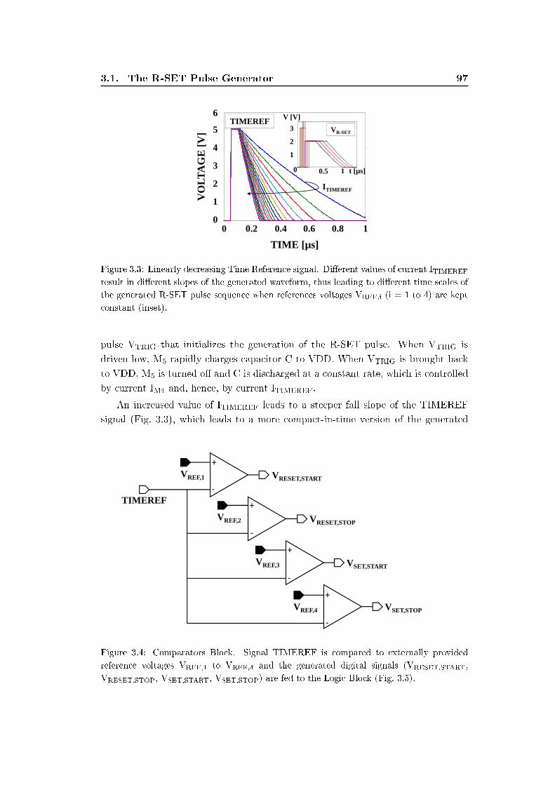
3.1. The R-SET Pulse Generator 97
1
2
3
4
5
0
6
0
VO
LTA
GE
[V]
TIME [µs]
0.2 0.4 0.6 0.8 1
ITIMEREF
t [µs]
V [V]
3
2
0.5 1
1
VR-SET
0
TIMEREF
Figure 3.3: Linearly decreasing Time Reference signal. Dierent values of current ITIMEREFresult in dierent slopes of the generated waveform, thus leading to dierent time scales of
the generated R-SET pulse sequence when references voltages VREF,i (i = 1 to 4) are kept
constant (inset).
pulse VTRIG that initializes the generation of the R-SET pulse. When VTRIG is
driven low, M5 rapidly charges capacitor C to VDD. When VTRIG is brought back
to VDD, M5 is turned o and C is discharged at a constant rate, which is controlled
by current IM4 and, hence, by current ITIMEREF.
An increased value of ITIMEREF leads to a steeper fall slope of the TIMEREF
signal (Fig. 3.3), which leads to a more compact-in-time version of the generated
+
+
+
+
-
TIMEREF
-
-
-
VREF,1
VREF,2
VREF,3
VREF,4
VRESET,START
VRESET,STOP
VSET,START
VSET,STOP
Figure 3.4: Comparators Block. Signal TIMEREF is compared to externally provided
reference voltages VREF,1 to VREF,4 and the generated digital signals (VRESET,START,
VRESET,STOP, VSET,START, VSET,STOP) are fed to the Logic Block (Fig. 3.5).
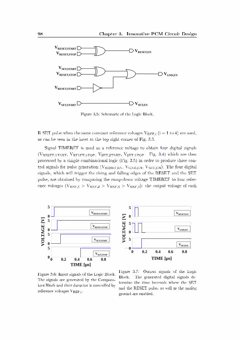
98 Chapter 3. Innovative PCM Circuit Design
VRESET,START
VRESET,STOP
VSET,START
VRESET,STOP
VRESET,START
VSET,START
VRESET,EN
VGND,EN
VSET,EN
Figure 3.5: Schematic of the Logic Block.
R-SET pulse when the same constant reference voltages VREF,i (i = 1 to 4) are used,
as can be seen in the inset at the top right corner of Fig. 3.3.
Signal TIMEREF is used as a reference voltage to obtain four digital signals
(VRESET,START, VRESET,STOP, VSET,START, VSET,STOP - Fig. 3.4) which are then
processed by a simple combinational logic (Fig. 3.5) in order to produce three con-
trol signals for pulse generation (VRESET,EN, VGND,EN, VSET,EN). The four digital
signals, which will trigger the rising and falling edges of the RESET and the SET
pulse, are obtained by comparing the ramp-down voltage TIMEREF to four refer-
ence voltages (VREF,1 > VREF,2 > VREF,3 > VREF,4): the output voltage of each
TIME [µs]
0
50
50
50
5
VO
LTA
GE
[V]
VRESET,START
VRESET,STOP
VSET,START
VSET,STOP
0 0.2 0.4 0.6 0.8
Figure 3.6: Input signals of the Logic Block.
The signals are generated by the Compara-
tors Block and their duration is controlled by
reference voltages VREF,i.
0
VO
LTA
GE
[V]
5
5
5
0
0
0 0.2 0.4 0.6 0.8
TIME [µs]
VRESET,EN
VGND,EN
VSET,EN
Figure 3.7: Output signals of the Logic
Block. The generated digital signals de-
termine the time intervals where the SET
and the RESET pulse, as well as the analog
ground are enabled.
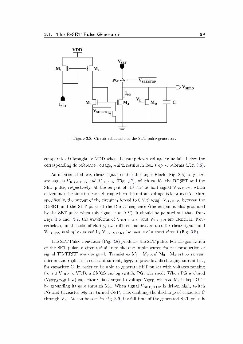
3.1. The R-SET Pulse Generator 99
M3 M4
VDD
VSET,O
M1
ISET
M2
PG
VSET
C
VSET,STOP
VD MD
VSET,STOP
IM4
Figure 3.8: Circuit schematic of the SET pulse generator.
comparator is brought to VDD when the ramp-down voltage value falls below the
corresponding dc reference voltage, which results in four step waveforms (Fig. 3.6).
As mentioned above, these signals enable the Logic Block (Fig. 3.5) to gener-
ate signals VRESET,EN and VSET,EN (Fig. 3.7), which enable the RESET and the
SET pulse, respectively, at the output of the circuit and signal VGND,EN, which
determines the time intervals during which the output voltage is kept at 0 V. More
specically, the output of the circuit is forced to 0 V through VGND,EN between the
RESET and the SET pulse of the R-SET sequence (the output is also grounded
by the SET pulse when this signal is at 0 V). It should be pointed out that, from
Figs. 3.6 and 3.7, the waveforms of VSET,START and VSET,EN are identical. Nev-
ertheless, for the sake of clarity, two dierent names are used for these signals and
VSET,EN is simply derived by VSET,START by means of a short circuit (Fig. 3.5).
The SET Pulse Generator (Fig. 3.8) produces the SET pulse. For the generation
of the SET pulse, a circuit similar to the one implemented for the production of
signal TIMEREF was designed. Transistors M1 - M2 and M3 - M4 act as current
mirrors and replicate a constant current, ISET, to provide a discharging current IM4,
for capacitor C. In order to be able to generate SET pulses with voltages ranging
from 0 V up to VDD, a CMOS analog switch, PG, was used. When PG is closed
(VSET,STOP low) capacitor C is charged to voltage VSET, whereas M4 is kept OFF
by grounding its gate through M5. When signal VSET,STOP is driven high, switch
PG and transistor M5 are turned OFF, thus enabling the discharge of capacitor C
through M4. As can be seen in Fig. 3.9, the fall time of the generated SET pulse is
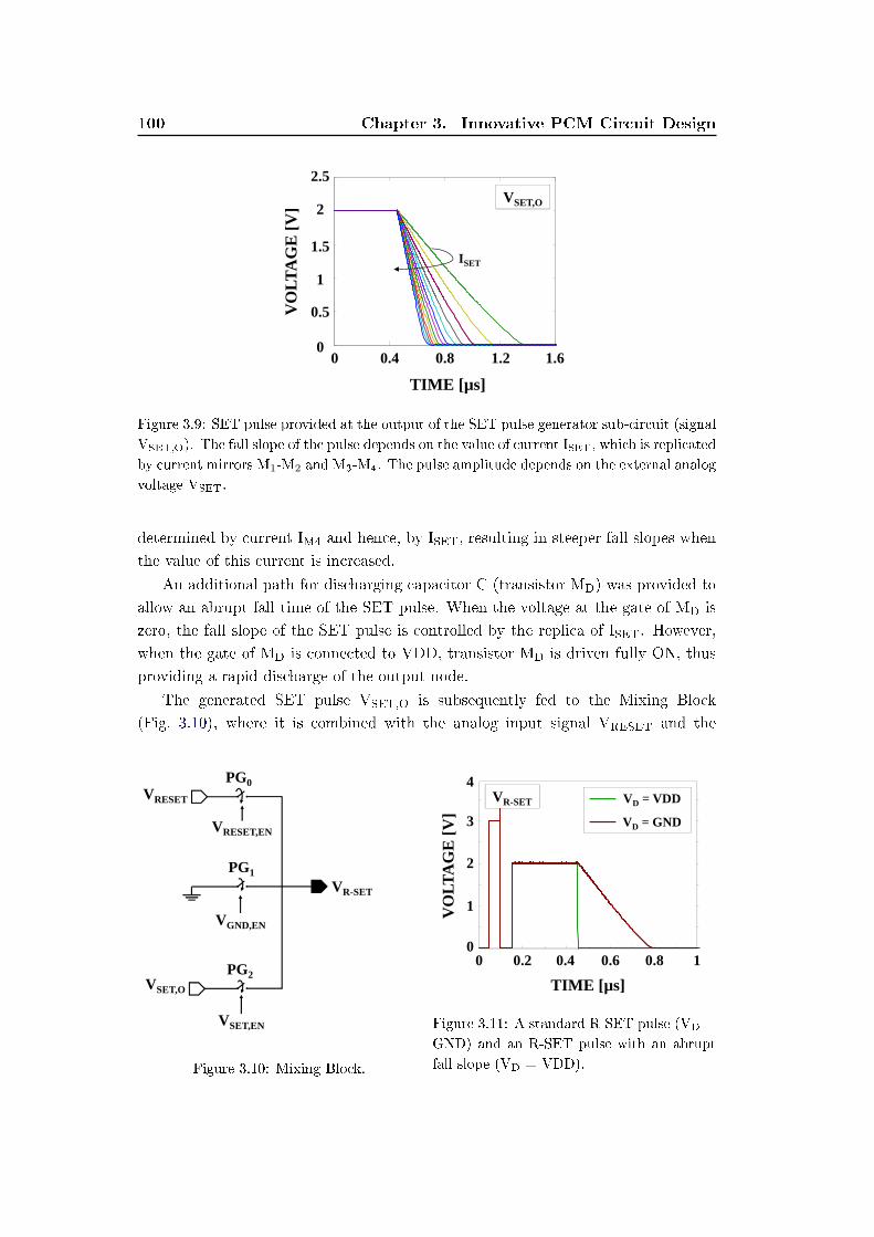
100 Chapter 3. Innovative PCM Circuit Design
5.2 7.6 10 12.4
0.5
0
VO
LTA
GE
[V]
TIME [µs]
0.4 0.8 1.2 1.60
1
1.5
2
2.5
ISET
VSET,O
Figure 3.9: SET pulse provided at the output of the SET pulse generator sub-circuit (signal
VSET,O). The fall slope of the pulse depends on the value of current ISET, which is replicated
by current mirrors M1-M2 and M3-M4. The pulse amplitude depends on the external analog
voltage VSET.
determined by current IM4 and hence, by ISET, resulting in steeper fall slopes when
the value of this current is increased.
An additional path for discharging capacitor C (transistor MD) was provided to
allow an abrupt fall time of the SET pulse. When the voltage at the gate of MD is
zero, the fall slope of the SET pulse is controlled by the replica of ISET. However,
when the gate of MD is connected to VDD, transistor MD is driven fully ON, thus
providing a rapid discharge of the output node.
The generated SET pulse VSET,O is subsequently fed to the Mixing Block
(Fig. 3.10), where it is combined with the analog input signal VRESET and the
VR-SET
PG0
PG2
VRESET
VSET,O
PG1
VRESET,EN
VGND,EN
VSET,EN
Figure 3.10: Mixing Block.
1
2
3
4
00
VO
LTA
GE
[V]
TIME [µs]
0.2 0.4 0.6 0.8 1
VD = VDD
VD = GND
VR-SET
Figure 3.11: A standard R-SET pulse (VD =
GND) and an R-SET pulse with an abrupt
fall slope (VD = VDD).
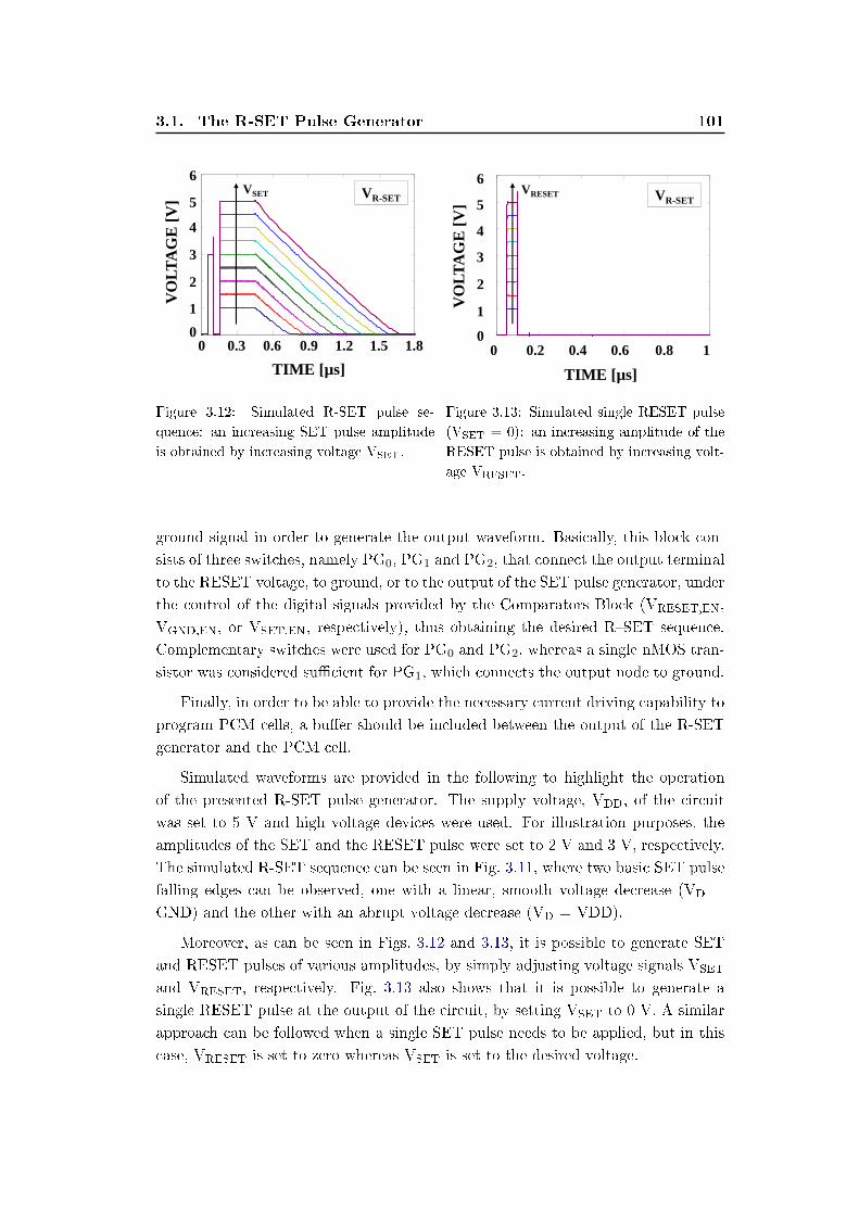
3.1. The R-SET Pulse Generator 101
0.4 0.7 1 1.3 1.6 1.9
VO
LTA
GE
[V]
TIME [µs]
1
2
3
4
5
0
VSET
0 0.3 0.6 1.51.2 1.80.9
6VR-SET
Figure 3.12: Simulated R-SET pulse se-
quence: an increasing SET pulse amplitude
is obtained by increasing voltage VSET.
0 0 0.000001 0.000001 0.000001
1
2
3
4
5
0
6
0
VO
LTA
GE
[V]
TIME [µs]
0.2 0.4 0.6 0.8 1
VRESET VR-SET
Figure 3.13: Simulated single RESET pulse
(VSET = 0): an increasing amplitude of the
RESET pulse is obtained by increasing volt-
age VRESET.
ground signal in order to generate the output waveform. Basically, this block con-
sists of three switches, namely PG0, PG1 and PG2, that connect the output terminal
to the RESET voltage, to ground, or to the output of the SET pulse generator, under
the control of the digital signals provided by the Comparators Block (VRESET,EN,
VGND,EN, or VSET,EN, respectively), thus obtaining the desired RSET sequence.
Complementary switches were used for PG0 and PG2, whereas a single nMOS tran-
sistor was considered sucient for PG1, which connects the output node to ground.
Finally, in order to be able to provide the necessary current driving capability to
program PCM cells, a buer should be included between the output of the R-SET
generator and the PCM cell.
Simulated waveforms are provided in the following to highlight the operation
of the presented R-SET pulse generator. The supply voltage, VDD, of the circuit
was set to 5 V and high voltage devices were used. For illustration purposes, the
amplitudes of the SET and the RESET pulse were set to 2 V and 3 V, respectively.
The simulated R-SET sequence can be seen in Fig. 3.11, where two basic SET pulse
falling edges can be observed, one with a linear, smooth voltage decrease (VD =
GND) and the other with an abrupt voltage decrease (VD = VDD).
Moreover, as can be seen in Figs. 3.12 and 3.13, it is possible to generate SET
and RESET pulses of various amplitudes, by simply adjusting voltage signals VSET
and VRESET, respectively. Fig. 3.13 also shows that it is possible to generate a
single RESET pulse at the output of the circuit, by setting VSET to 0 V. A similar
approach can be followed when a single SET pulse needs to be applied, but in this
case, VRESET is set to zero whereas VSET is set to the desired voltage.
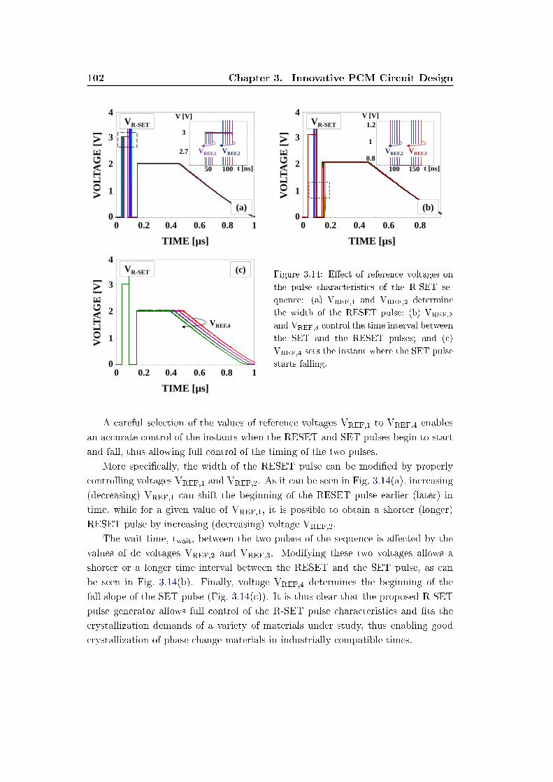
102 Chapter 3. Innovative PCM Circuit Design
1
2
3
4
00
VO
LTA
GE
[V]
TIME [µs]
0.2 0.4 0.6 0.8 1
t [ns]
VREF,2VREF,1
V [V]
3
2.7
50 100
VR-SET
(a)
1
2
3
4
00
VO
LTA
GE
[V]
TIME [µs]
0.2 0.4 0.6 0.8
t [ns]
VREF,3VREF,2
V [V]1.2
1
100 150
0.8
VR-SET
(b)
1
2
3
4
00
VO
LTA
GE
[V]
TIME [µs]
0.2 0.4 0.6 0.8 1
VREF,4
VR-SET (c) Figure 3.14: Eect of reference voltages on
the pulse characteristics of the R-SET se-
quence: (a) VREF,1 and VREF,2 determine
the width of the RESET pulse; (b) VREF,2and VREF,3 control the time interval between
the SET and the RESET pulses; and (c)
VREF,4 sets the instant where the SET pulse
starts falling.
A careful selection of the values of reference voltages VREF,1 to VREF,4 enables
an accurate control of the instants when the RESET and SET pulses begin to start
and fall, thus allowing full control of the timing of the two pulses.
More specically, the width of the RESET pulse can be modied by properly
controlling voltages VREF,1 and VREF,2. As it can be seen in Fig. 3.14(a), increasing
(decreasing) VREF,1 can shift the beginning of the RESET pulse earlier (later) in
time, while for a given value of VREF,1, it is possible to obtain a shorter (longer)
RESET pulse by increasing (decreasing) voltage VREF,2.
The wait time, twait, between the two pulses of the sequence is aected by the
values of dc voltages VREF,2 and VREF,3. Modifying these two voltages allows a
shorter or a longer time interval between the RESET and the SET pulse, as can
be seen in Fig. 3.14(b). Finally, voltage VREF,4 determines the beginning of the
fall slope of the SET pulse (Fig. 3.14(c)). It is thus clear that the proposed R-SET
pulse generator allows full control of the R-SET pulse characteristics and ts the
crystallization demands of a variety of materials under study, thus enabling good
crystallization of phase change materials in industrially compatible times.
3.2. Pulse Generator for Optimized Temperature Prole 103
3.2 Pulse Generator for Optimized Temperature Prole
In order to perform a SET programming operation and bring the memory cell
to its LRS, the electrical pulse applied to the device must induce a temperature
higher than the crystallization temperature of the chalcogenide material. A follow-
ing smooth decrease of the programming voltage and, hence, of the temperature
of the active material of the memory cell is necessary to bring the cell to its SET
state. However, since the drift coecient of the Low Resistance State in Ge-rich
GST PCM is not negligible when the chalcogenide material is not fully recrystal-
lized, it is necessary to come up with an appropriate programming technique able
to provide an optimum crystallization to the cell and, therefore, minimize the resis-
tance distribution dispersion of the SET state, possibly by means of a single-pulse
procedure.
In this Section, we propose a technique to optimally crystallize phase change
materials. A linear temperature prole has been shown to lead to an optimal crys-
tal size distribution in a batch crystallizer [126], highlighting the need for accurate
temperature control during programming. Therefore, our solution consists in gen-
erating a programming voltage pulse which ensures a constant decrease rate of the
programming temperature inside the cell after the pulse plateau.
3.2.1 Voltage Controlled Temperature
In order to optimize the SET state resistance distribution and obtain a plain crys-
talline state, possibly not aected by drift, a suitable programming pulse able to
deliver an appropriate temperature prole to the cell should be generated. The pur-
pose of the pulse is to generate a linear decrease of the programming temperature,
as required for optimum crystallization of the phase change material.
The temperature developed in the active region of the memory cell is given by
T = TEXT + RTHP = TEXT + RTHV2PROG
RCELL(3.1)
where TEXT is the external temperature, RTH and RCELL are the thermal and the
electrical resistance of the cell, respectively, and P is the power developed in the cell
when a voltage VPROG is applied across the cell.
Studying the temperature evolution over time and assuming the thermal time
constants of the cell to be negligible with respect to dVPROG/dt, we obtain
dTdt
=d(RTH
V2PROG
RCELL
)dt
⇒ dTdt
= 2RTH
RCELL
dVPROG
dtVPROG. (3.2)
It is thus clear that the derivative of the temperature over time is proportional to
the product of the applied voltage and its derivative over time (RTH/RCELL can be
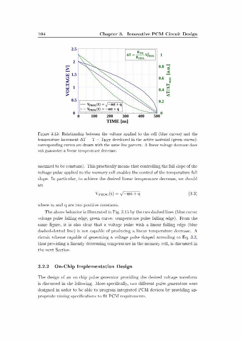
104 Chapter 3. Innovative PCM Circuit Design
VO
LT
AG
E [
V]
ΔT
/ΔT
max
[a.u
.]
1.5
2.5
2
1
0.5
0100 2000 300 400 500
0.4
0.2
0
0.6
0.8
1
TIME [ns]
= − +
= − +
Δ =
Figure 3.15: Relationship between the voltage applied to the cell (blue curves) and the
temperature increment ∆T = T − TEXT developed in the active material (green curves):
corresponding curves are drawn with the same line pattern. A linear voltage decrease does
not guarantee a linear temperature decrease.
assumed to be constant). This practically means that controlling the fall slope of the
voltage pulse applied to the memory cell enables the control of the temperature fall
slope. In particular, to achieve the desired linear temperature decrease, we should
set
VPROG(t) =√−mt+ q (3.3)
where m and q are two positive constants.
The above behavior is illustrated in Fig. 3.15 by the two dashed lines (blue curve:
voltage pulse falling edge; green curve: temperature pulse falling edge). From the
same gure, it is also clear that a voltage pulse with a linear falling edge (blue
dashed-dotted line) is not capable of producing a linear temperature decrease. A
circuit scheme capable of generating a voltage pulse shaped according to Eq. 3.3,
thus providing a linearly decreasing temperature in the memory cell, is discussed in
the next Section.
3.2.2 On-Chip Implementation Design
The design of an on-chip pulse generator providing the desired voltage waveform
is discussed in the following. More specically, two dierent pulse generators were
designed in order to be able to program integrated PCM devices by providing ap-
propriate timing specications to t PCM requirements.
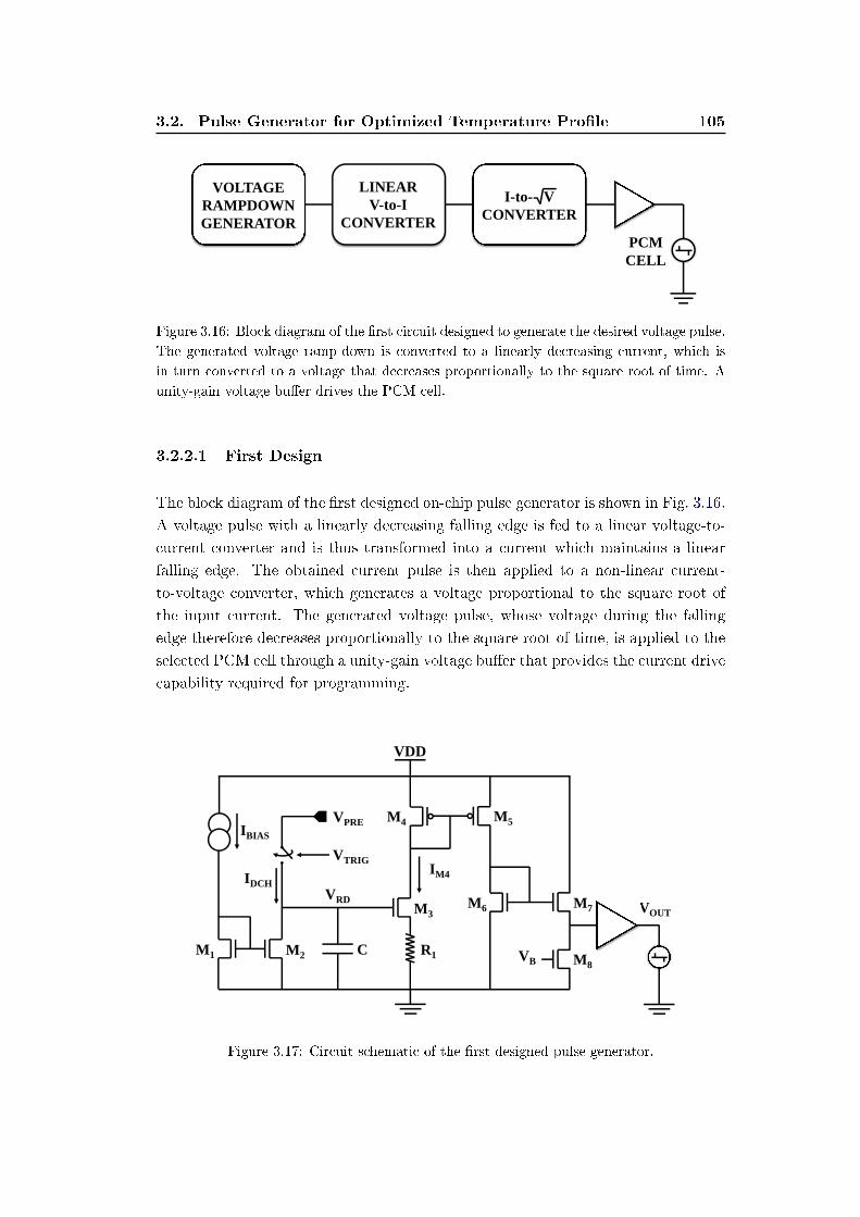
3.2. Pulse Generator for Optimized Temperature Prole 105
VOLTAGE RAMPDOWN GENERATOR
LINEAR V-to-I
CONVERTER
I-to- V CONVERTER
PCM CELL
Figure 3.16: Block diagram of the rst circuit designed to generate the desired voltage pulse.
The generated voltage ramp-down is converted to a linearly decreasing current, which is
in turn converted to a voltage that decreases proportionally to the square root of time. A
unity-gain voltage buer drives the PCM cell.
3.2.2.1 First Design
The block diagram of the rst designed on-chip pulse generator is shown in Fig. 3.16.
A voltage pulse with a linearly decreasing falling edge is fed to a linear voltage-to-
current converter and is thus transformed into a current which maintains a linear
falling edge. The obtained current pulse is then applied to a non-linear current-
to-voltage converter, which generates a voltage proportional to the square root of
the input current. The generated voltage pulse, whose voltage during the falling
edge therefore decreases proportionally to the square root of time, is applied to the
selected PCM cell through a unity-gain voltage buer that provides the current drive
capability required for programming.
M1 M2
M3
M4 M5
C R1
VDD
VPRE
VOUT
VTRIG
VRD
IBIAS
M7M6
M8
IM4
VB
IDCH
Figure 3.17: Circuit schematic of the rst designed pulse generator.
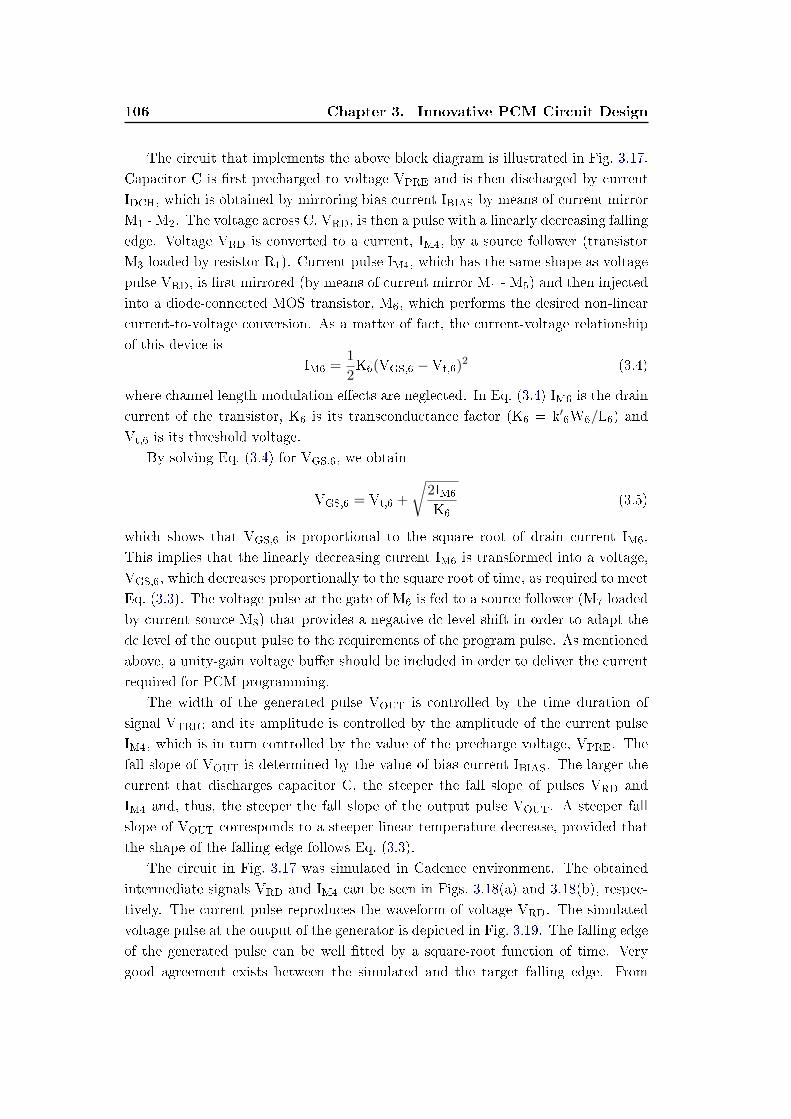
106 Chapter 3. Innovative PCM Circuit Design
The circuit that implements the above block diagram is illustrated in Fig. 3.17.
Capacitor C is rst precharged to voltage VPRE and is then discharged by current
IDCH, which is obtained by mirroring bias current IBIAS by means of current mirror
M1 - M2. The voltage across C, VRD, is then a pulse with a linearly decreasing falling
edge. Voltage VRD is converted to a current, IM4, by a source follower (transistor
M3 loaded by resistor R1). Current pulse IM4, which has the same shape as voltage
pulse VRD, is rst mirrored (by means of current mirror M4 - M5) and then injected
into a diode-connected MOS transistor, M6, which performs the desired non-linear
current-to-voltage conversion. As a matter of fact, the current-voltage relationship
of this device is
IM6 =1
2K6(VGS,6 −Vt,6)
2 (3.4)
where channel length modulation eects are neglected. In Eq. (3.4) IM6 is the drain
current of the transistor, K6 is its transconductance factor (K6 = k′6W6/L6) and
Vt,6 is its threshold voltage.
By solving Eq. (3.4) for VGS,6, we obtain
VGS,6 = Vt,6 +
√2IM6
K6(3.5)
which shows that VGS,6 is proportional to the square root of drain current IM6.
This implies that the linearly decreasing current IM6 is transformed into a voltage,
VGS,6, which decreases proportionally to the square root of time, as required to meet
Eq. (3.3). The voltage pulse at the gate of M6 is fed to a source follower (M7 loaded
by current source M8) that provides a negative dc level shift in order to adapt the
dc level of the output pulse to the requirements of the program pulse. As mentioned
above, a unity-gain voltage buer should be included in order to deliver the current
required for PCM programming.
The width of the generated pulse VOUT is controlled by the time duration of
signal VTRIG and its amplitude is controlled by the amplitude of the current pulse
IM4, which is in turn controlled by the value of the precharge voltage, VPRE. The
fall slope of VOUT is determined by the value of bias current IBIAS. The larger the
current that discharges capacitor C, the steeper the fall slope of pulses VRD and
IM4 and, thus, the steeper the fall slope of the output pulse VOUT. A steeper fall
slope of VOUT corresponds to a steeper linear temperature decrease, provided that
the shape of the falling edge follows Eq. (3.3).
The circuit in Fig. 3.17 was simulated in Cadence environment. The obtained
intermediate signals VRD and IM4 can be seen in Figs. 3.18(a) and 3.18(b), respec-
tively. The current pulse reproduces the waveform of voltage VRD. The simulated
voltage pulse at the output of the generator is depicted in Fig. 3.19. The falling edge
of the generated pulse can be well tted by a square-root function of time. Very
good agreement exists between the simulated and the target falling edge. From
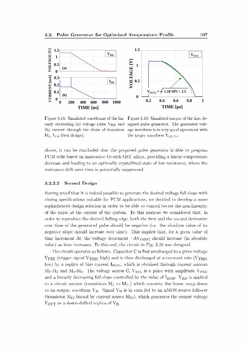
3.2. Pulse Generator for Optimized Temperature Prole 107
VO
LTA
GE
[V]
200TIME [ns]
0
1.5
1
0.5
0
0.3
0.2
0.1
CU
RR
EN
T [m
A]
400 600 800 10000
VRD
IM4
(a)
(b)
Figure 3.18: Simulated waveforms of the lin-
early decreasing (a) voltage pulse VRD and
(b) current through the drain of transistor
M4, IM4 (rst design).
0.2 0.4 0.6 0.8 1
VOUT,i = - 1.18 106t + 2.5 .
0
1
0.5
1.5
VO
LTA
GE
[V]
TIME [µs]
VOUT
Figure 3.19: Simulated output of the rst de-
signed pulse generator. The generated volt-
age waveform is in very good agreement with
the target waveform VOUT,i.
above, it can be concluded that the proposed pulse generator is able to program
PCM cells based on innovative Ge-rich GST alloys, providing a linear temperature
decrease and leading to an optimally crystallized state of low resistance, where the
resistance drift over time is potentially suppressed.
3.2.2.2 Second Design
Having proof that it is indeed possible to generate the desired voltage fall slope with
timing specications suitable for PCM applications, we decided to develop a more
sophisticated design solution in order to be able to control better the non-linearity
of the pulse at the output of the system. To this purpose we considered that, in
order to reproduce the desired falling edge, both the rst and the second derivative
over time of the generated pulse should be negative (i.e. the absolute value of its
negative slope should increase over time). This implies that, for a given value of
time increment ∆t, the voltage decrement −∆VPROG should increase (in absolute
value) as time increases. To this end, the circuit in Fig. 3.20 was designed.
The circuit operates as follows. Capacitor C is rst precharged to a given voltage
VPRE (trigger signal VTRIG high) and is then discharged at a constant rate (VTRIG
low) by a replica of bias current IBIAS, which is obtained through current mirrors
M1-M2 and M3-M4. The voltage across C, VRD, is a pulse with amplitude VPRE
and a linearly decreasing fall slope controlled by the value of IBIAS. VRD is applied
to a circuit section (transistors M5 to M11) which converts the linear ramp-down
to an output waveform VB. Signal VB is in turn fed to an nMOS source follower
(transistor M12 biased by current source M13), which generates the output voltage
VOUT as a down-shifted replica of VB.
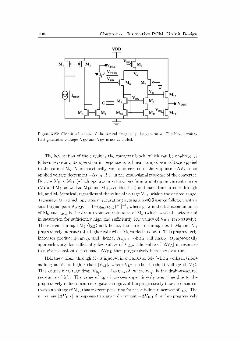
108 Chapter 3. Innovative PCM Circuit Design
VOUT
VPRE
VBP
VBN
VBN
VRD
C
IBIAS
VDD
M1 M2
M3 M4
M5
M6
M8
M10
M9
M11
M7
M12
M13
VTRIG VA
VB
Figure 3.20: Circuit schematic of the second designed pulse generator. The bias circuitry
that generates voltages VBN and VBP is not included.
The key section of the circuit is the converter block, which can be analyzed as
follows regarding its operation in response to a linear ramp-down voltage applied
to the gate of M6. More specically, we are interested in the response −∆VB to an
applied voltage decrement −∆VRD, i.e. in the small-signal response of the converter.
Devices M8 to M11 (which operate in saturation) form a unity-gain current mirror
(M8 and M9, as well as M10 and M11, are identical) and make the currents through
M6 and M7 identical, regardless of the value of voltage VRD within the desired range.
Transistor M6 (which operates in saturation) acts as a pMOS source follower, with a
small-signal gain AA,RD = [1+(gm,6rds,5)−1]−1, where gm,6 is the transconductance
of M6 and rds,5 is the drain-to-source resistance of M5 (which works in triode and
in saturation for suciently high and suciently low values of VRD, respectively).
The current through M5 (IM5) and, hence, the currents through both M6 and M7
progressively increase (at a higher rate when M5 works in triode). This progressively
increases product gm,6rds,5 and, hence, AA,RD, which will nally asymptotically
approach unity for suciently low values of VRD. The value of |∆VA| in response
to a given constant decrement −∆VRD then progressively increases over time.
Half the current through M5 is injected into transistor M7 (which works in triode
as long as VB is higher than |Vt,7|, where Vt,7 is the threshold voltage of M7).
This causes a voltage drop VB,A = IM5rds,7/2, where rds,7 is the drain-to-source
resistance of M7. The value of rds,7 increases super-linearly over time due to the
progressively reduced source-to-gate voltage and the progressively increased source-
to-drain voltage of M7, thus overcompensating for the sub-linear increase of IM5. The
increment |∆VB,A| in response to a given decrement −∆VRD therefore progressively
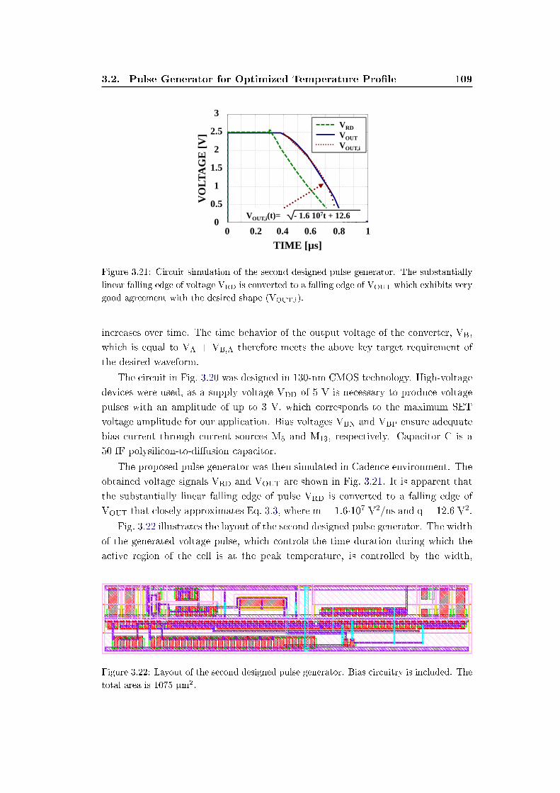
3.2. Pulse Generator for Optimized Temperature Prole 109
VRDVOUTVOUT,i
VOUT,i(t)= - 1.6 107t + 12.6
VO
LTA
GE
[V]
0
1
2
3
0.20
TIME [µs]1
0.5
1.5
2.5
0.4 0.6 0.8
Figure 3.21: Circuit simulation of the second designed pulse generator. The substantially
linear falling edge of voltage VRD is converted to a falling edge of VOUT which exhibits very
good agreement with the desired shape (VOUT,i).
increases over time. The time behavior of the output voltage of the converter, VB,
which is equal to VA + VB,A therefore meets the above key target requirement of
the desired waveform.
The circuit in Fig. 3.20 was designed in 130-nm CMOS technology. High-voltage
devices were used, as a supply voltage VDD of 5 V is necessary to produce voltage
pulses with an amplitude of up to 3 V, which corresponds to the maximum SET
voltage amplitude for our application. Bias voltages VBN and VBP ensure adequate
bias current through current sources M5 and M13, respectively. Capacitor C is a
50 fF polysilicon-to-diusion capacitor.
The proposed pulse generator was then simulated in Cadence environment. The
obtained voltage signals VRD and VOUT are shown in Fig. 3.21. It is apparent that
the substantially linear falling edge of pulse VRD is converted to a falling edge of
VOUT that closely approximates Eq. 3.3, where m = 1.6·107 V2/ns and q = 12.6 V2.
Fig. 3.22 illustrates the layout of the second designed pulse generator. The width
of the generated voltage pulse, which controls the time duration during which the
active region of the cell is at the peak temperature, is controlled by the width,
Figure 3.22: Layout of the second designed pulse generator. Bias circuitry is included. The
total area is 1075 µm2.
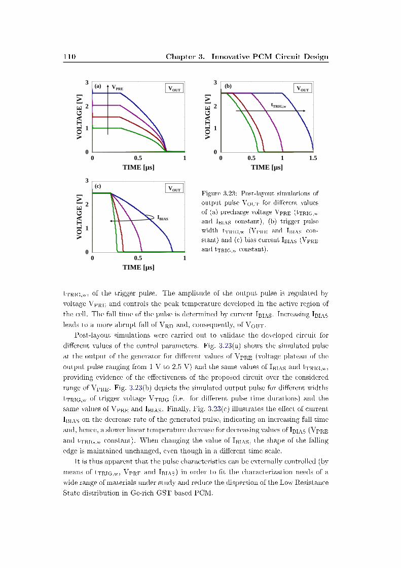
110 Chapter 3. Innovative PCM Circuit Design
VPRE
VO
LTA
GE
[V]
0
1
2
3
0.50
TIME [µs]1
(a) VOUT
VO
LTA
GE
[V]
0
1
2
3
0.50
TIME [µs]1 1.5
tTRIG,w
(b) VOUT
VO
LTA
GE
[V]
0
1
2
3
0.50
TIME [µs]1
IBIAS
(c) VOUTFigure 3.23: Post-layout simulations of
output pulse VOUT for dierent values
of (a) precharge voltage VPRE (tTRIG,wand IBIAS constant), (b) trigger pulse
width tTRIG,w (VPRE and IBIAS con-
stant) and (c) bias current IBIAS (VPREand tTRIG,w constant).
tTRIG,w, of the trigger pulse. The amplitude of the output pulse is regulated by
voltage VPRE and controls the peak temperature developed in the active region of
the cell. The fall time of the pulse is determined by current IBIAS. Increasing IBIASleads to a more abrupt fall of VRD and, consequently, of VOUT.
Post-layout simulations were carried out to validate the developed circuit for
dierent values of the control parameters. Fig. 3.23(a) shows the simulated pulse
at the output of the generator for dierent values of VPRE (voltage plateau of the
output pulse ranging from 1 V to 2.5 V) and the same values of IBIAS and tTRIG,w,
providing evidence of the eectiveness of the proposed circuit over the considered
range of VPRE. Fig. 3.23(b) depicts the simulated output pulse for dierent widths
tTRIG,w of trigger voltage VTRIG (i.e. for dierent pulse time durations) and the
same values of VPRE and IBIAS. Finally, Fig. 3.23(c) illustrates the eect of current
IBIAS on the decrease rate of the generated pulse, indicating an increasing fall time
and, hence, a slower linear temperature decrease for decreasing values of IBIAS (VPRE
and tTRIG,w constant). When changing the value of IBIAS, the shape of the falling
edge is maintained unchanged, even though in a dierent time scale.
It is thus apparent that the pulse characteristics can be externally controlled (by
means of tTRIG,w, VPRE and IBIAS) in order to t the characterization needs of a
wide range of materials under study and reduce the dispersion of the Low Resistance
State distribution in Ge-rich GST based PCM.
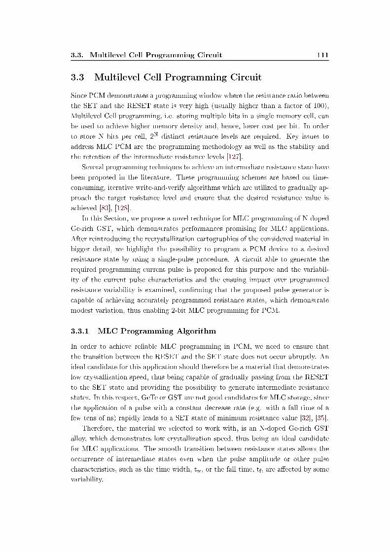
3.3. Multilevel Cell Programming Circuit 111
3.3 Multilevel Cell Programming Circuit
Since PCM demonstrates a programming window where the resistance ratio between
the SET and the RESET state is very high (usually higher than a factor of 100),
Multilevel Cell programming, i.e. storing multiple bits in a single memory cell, can
be used to achieve higher memory density and, hence, lower cost per bit. In order
to store N bits per cell, 2N distinct resistance levels are required. Key issues to
address MLC PCM are the programming methodology as well as the stability and
the retention of the intermediate resistance levels [127].
Several programming techniques to achieve an intermediate resistance state have
been proposed in the literature. These programming schemes are based on time-
consuming, iterative write-and-verify algorithms which are utilized to gradually ap-
proach the target resistance level and ensure that the desired resistance value is
achieved [83], [128].
In this Section, we propose a novel technique for MLC programming of N-doped
Ge-rich GST, which demonstrates performances promising for MLC applications.
After reintroducing the recrystallization cartographies of the considered material in
bigger detail, we highlight the possibility to program a PCM device to a desired
resistance state by using a single-pulse procedure. A circuit able to generate the
required programming current pulse is proposed for this purpose and the variabil-
ity of the current pulse characteristics and the ensuing impact over programmed
resistance variability is examined, conrming that the proposed pulse generator is
capable of achieving accurately programmed resistance states, which demonstrate
modest variation, thus enabling 2-bit MLC programming for PCM.
3.3.1 MLC Programming Algorithm
In order to achieve reliable MLC programming in PCM, we need to ensure that
the transition between the RESET and the SET state does not occur abruptly. An
ideal candidate for this application should therefore be a material that demonstrates
low crystallization speed, thus being capable of gradually passing from the RESET
to the SET state and providing the possibility to generate intermediate resistance
states. In this respect, GeTe or GST are not good candidates for MLC storage, since
the application of a pulse with a constant decrease rate (e.g. with a fall time of a
few tens of ns) rapidly leads to a SET state of minimum resistance value [32], [35].
Therefore, the material we selected to work with, is an N-doped Ge-rich GST
alloy, which demonstrates low crystallization speed, thus being an ideal candidate
for MLC applications. The smooth transition between resistance states allows the
occurrence of intermediate states even when the pulse amplitude or other pulse
characteristics, such as the time width, tw, or the fall time, tf, are aected by some
variability.
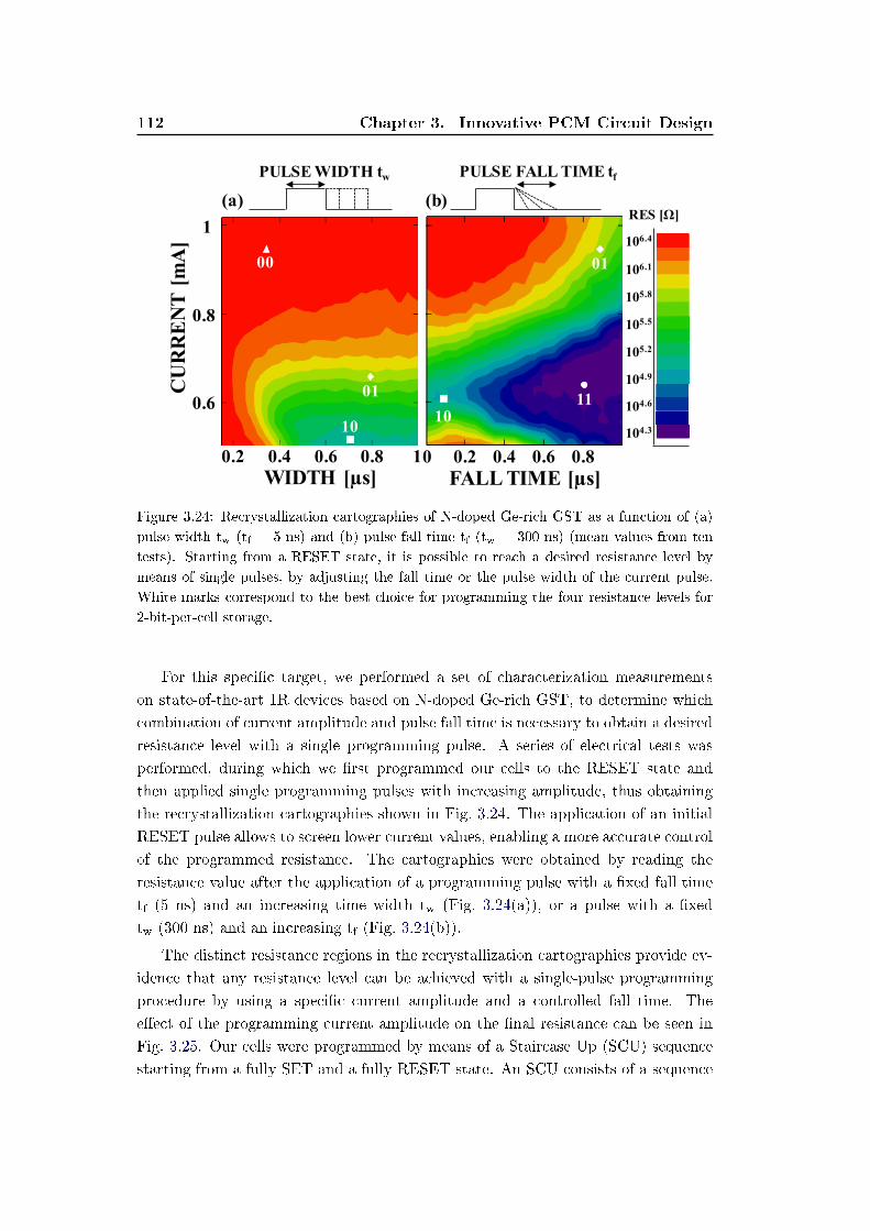
112 Chapter 3. Innovative PCM Circuit Design
RES [Ω]
106.4
104.3
104.6
104.9
105.2
105.5
105.8
106.1
CU
RR
EN
T [m
A]
0.6
0.8
1
WIDTH [µs]0.80.2
PULSE WIDTH tw
(a)
00
10
0.4 0.6 1FALL TIME [µs]
0.80.2 0.4
PULSE FALL TIME tf
(b)
11
01
0.60
0110
Figure 3.24: Recrystallization cartographies of N-doped Ge-rich GST as a function of (a)
pulse width tw (tf = 5 ns) and (b) pulse fall time tf (tw = 300 ns) (mean values from ten
tests). Starting from a RESET state, it is possible to reach a desired resistance level by
means of single pulses, by adjusting the fall time or the pulse width of the current pulse.
White marks correspond to the best choice for programming the four resistance levels for
2-bit-per-cell storage.
For this specic target, we performed a set of characterization measurements
on state-of-the-art 1R devices based on N-doped Ge-rich GST, to determine which
combination of current amplitude and pulse fall time is necessary to obtain a desired
resistance level with a single programming pulse. A series of electrical tests was
performed, during which we rst programmed our cells to the RESET state and
then applied single programming pulses with increasing amplitude, thus obtaining
the recrystallization cartographies shown in Fig. 3.24. The application of an initial
RESET pulse allows to screen lower current values, enabling a more accurate control
of the programmed resistance. The cartographies were obtained by reading the
resistance value after the application of a programming pulse with a xed fall time
tf (5 ns) and an increasing time width tw (Fig. 3.24(a)), or a pulse with a xed
tw (300 ns) and an increasing tf (Fig. 3.24(b)).
The distinct resistance regions in the recrystallization cartographies provide ev-
idence that any resistance level can be achieved with a single-pulse programming
procedure by using a specic current amplitude and a controlled fall time. The
eect of the programming current amplitude on the nal resistance can be seen in
Fig. 3.25. Our cells were programmed by means of a Staircase Up (SCU) sequence
starting from a fully SET and a fully RESET state. An SCU consists of a sequence
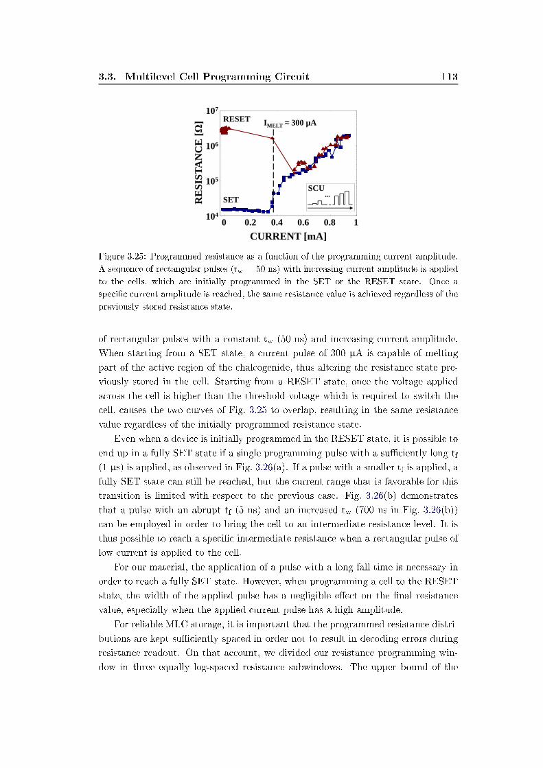
3.3. Multilevel Cell Programming Circuit 113
RE
SIS
TAN
CE
[Ω
]
105
CURRENT [mA]0 0.2 0.4 0.6 0.8 1
104
106
107
RESET
SET...
SCU
IMELT ≈ 300 µA
Figure 3.25: Programmed resistance as a function of the programming current amplitude.
A sequence of rectangular pulses (tw = 50 ns) with increasing current amplitude is applied
to the cells, which are initially programmed in the SET or the RESET state. Once a
specic current amplitude is reached, the same resistance value is achieved regardless of the
previously stored resistance state.
of rectangular pulses with a constant tw (50 ns) and increasing current amplitude.
When starting from a SET state, a current pulse of 300 µA is capable of melting
part of the active region of the chalcogenide, thus altering the resistance state pre-
viously stored in the cell. Starting from a RESET state, once the voltage applied
across the cell is higher than the threshold voltage which is required to switch the
cell, causes the two curves of Fig. 3.25 to overlap, resulting in the same resistance
value regardless of the initially programmed resistance state.
Even when a device is initially programmed in the RESET state, it is possible to
end up in a fully SET state if a single programming pulse with a suciently long tf(1 µs) is applied, as observed in Fig. 3.26(a). If a pulse with a smaller tf is applied, a
fully SET state can still be reached, but the current range that is favorable for this
transition is limited with respect to the previous case. Fig. 3.26(b) demonstrates
that a pulse with an abrupt tf (5 ns) and an increased tw (700 ns in Fig. 3.26(b))
can be employed in order to bring the cell to an intermediate resistance level. It is
thus possible to reach a specic intermediate resistance when a rectangular pulse of
low current is applied to the cell.
For our material, the application of a pulse with a long fall time is necessary in
order to reach a fully SET state. However, when programming a cell to the RESET
state, the width of the applied pulse has a negligible eect on the nal resistance
value, especially when the applied current pulse has a high amplitude.
For reliable MLC storage, it is important that the programmed resistance distri-
butions are kept suciently spaced in order not to result in decoding errors during
resistance readout. On that account, we divided our resistance programming win-
dow in three equally log-spaced resistance subwindows. The upper bound of the
114 Chapter 3. Innovative PCM Circuit Design
tf = 1 µstf = 0.5 µsR
ES
ISTA
NC
E [Ω
]
105
106
0.5 0.75
CURRENT [mA]1
104(a)
tw = 0.7 µstw = 0.1 µsR
ES
ISTA
NC
E [Ω
]
105
106
0.5 0.75
CURRENT [mA]1
104(b)
Figure 3.26: Programmed resistance as a function of the programming current amplitude
for dierent values of (a) pulse width tw (tf = 5 ns) and (b) pulse fall time tf (tw = 300 ns).
An increased tf is necessary to reach a stable Low Resistance State starting from a RESET
state. Increasing tw enables the programming of intermediate resistance states at lower
programming currents. A short tw at higher current amplitudes ensures a high-resistance
state that remains substantially constant in a wide programming current range.
overall programming window corresponds to a fully RESET state (state 00), which
can be achieved by a programming pulse with high amplitude and short fall time.
The lower bound of the programming window corresponds to the fully SET resis-
tance value (state 11), which is obtained by applying a programming pulse with
lower amplitude and long fall time. The programming conditions for states 00 and
11 can be easily derived from the recrystallization cartographies (deep red region
in Fig. 3.24(a) and deep purple region in Fig. 3.24(b), respectively). Intermediate
states 01 and 10 correspond to the upper and the lower bound of the intermediate
resistance subwindow, respectively.
We then investigated the cartographies for regions around the target intermedi-
ate resistance values, aiming at nding the programming conditions and the actual
target resistance values that ensure the minimum impact of the variation of the
programming pulse parameters over the obtained resistance.
To this end, we estimated which resistance level close to the target value shows
the least sensitivity to current amplitude variation and for which programming con-
ditions this resistance value can be achieved. Once this resistance level and the
corresponding programming conditions were found, a similar calculation was car-
ried out for the sensitivity of the programmed resistance to fall time variations. The
obtained states and the corresponding programming conditions are highlighted by
white marks in Fig. 3.24.
The choice of the best programming conditions to obtain a state 01 with low
sensitivity to programming condition variations is straightforward, when a pulse
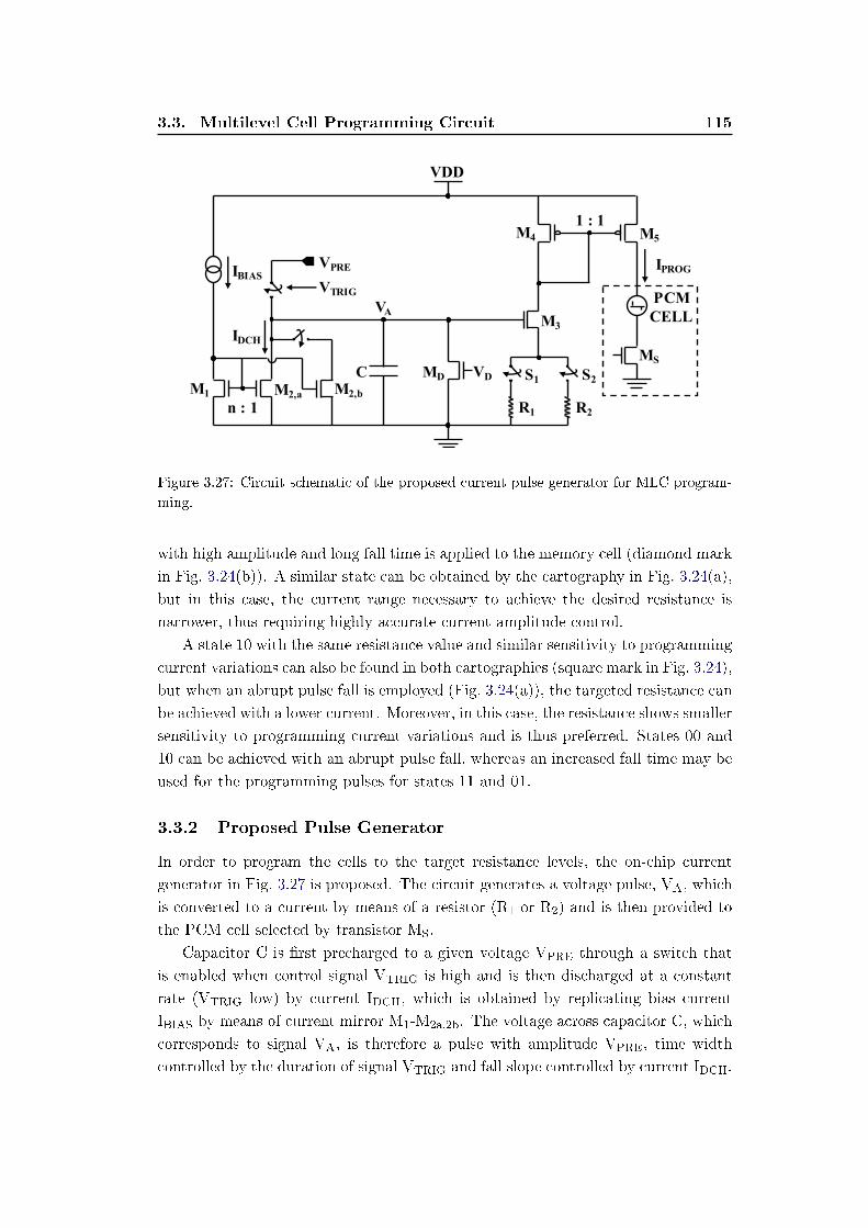
3.3. Multilevel Cell Programming Circuit 115
n : 1
1 : 1
M1 M2,a
MD
M3
M4 M5
C
R1 R2
VDD
VPRE IPROG
VTRIGVA
MS
IDCH
PCM CELL
S1 S2
IBIAS
VDM2,b
Figure 3.27: Circuit schematic of the proposed current pulse generator for MLC program-
ming.
with high amplitude and long fall time is applied to the memory cell (diamond mark
in Fig. 3.24(b)). A similar state can be obtained by the cartography in Fig. 3.24(a),
but in this case, the current range necessary to achieve the desired resistance is
narrower, thus requiring highly accurate current amplitude control.
A state 10 with the same resistance value and similar sensitivity to programming
current variations can also be found in both cartographies (square mark in Fig. 3.24),
but when an abrupt pulse fall is employed (Fig. 3.24(a)), the targeted resistance can
be achieved with a lower current. Moreover, in this case, the resistance shows smaller
sensitivity to programming current variations and is thus preferred. States 00 and
10 can be achieved with an abrupt pulse fall, whereas an increased fall time may be
used for the programming pulses for states 11 and 01.
3.3.2 Proposed Pulse Generator
In order to program the cells to the target resistance levels, the on-chip current
generator in Fig. 3.27 is proposed. The circuit generates a voltage pulse, VA, which
is converted to a current by means of a resistor (R1 or R2) and is then provided to
the PCM cell selected by transistor MS.
Capacitor C is rst precharged to a given voltage VPRE through a switch that
is enabled when control signal VTRIG is high and is then discharged at a constant
rate (VTRIG low) by current IDCH, which is obtained by replicating bias current
IBIAS by means of current mirror M1-M2a,2b. The voltage across capacitor C, which
corresponds to signal VA, is therefore a pulse with amplitude VPRE, time width
controlled by the duration of signal VTRIG and fall slope controlled by current IDCH.
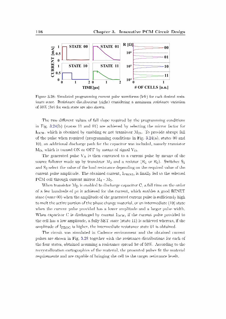
116 Chapter 3. Innovative PCM Circuit Design
1 20TIME[µs]
CU
RR
EN
T [m
A]
0
0.5
1
0
0.5
1
1 20
STATE 00 STATE 01
STATE 10 STATE 11
106
105
104
R [Ω]
# OF CELLS [a.u.]0 1
00
01
10
11
Figure 3.28: Simulated programming current pulse waveforms (left) for each desired resis-
tance state. Resistance distributions (right) considering a maximum resistance variation
of 50% (3σ) for each state are also shown.
The two dierent values of fall slope required by the programming conditions
in Fig. 3.24(b) (states 11 and 01) are achieved by selecting the mirror factor for
IDCH, which is obtained by enabling or not transistor M2b. To provide abrupt fall
of the pulse when required (programming conditions in Fig. 3.24(a), states 00 and
10), an additional discharge path for the capacitor was included, namely transistor
MD, which is turned ON or OFF by means of signal VD.
The generated pulse VA is then converted to a current pulse by means of the
source follower made up by transistor M3 and a resistor (R1 or R2). Switches S1and S2 select the value of the load resistance depending on the required value of the
current pulse amplitude. The obtained current, IPROG, is nally fed to the selected
PCM cell through current mirror M4 - M5.
When transistor MD is enabled to discharge capacitor C, a fall time on the order
of a few hundreds of ps is achieved for the current, which enables a good RESET
state (state 00) when the amplitude of the generated current pulse is suciently high
to melt the active portion of the phase change material, or an intermediate (10) state
when the current pulse provided has a lower amplitude and a larger pulse width.
When capacitor C is discharged by current IDCH, if the current pulse provided to
the cell has a low amplitude, a fully SET state (state 11) is achieved whereas, if the
amplitude of IPROG is higher, the intermediate resistance state 01 is obtained.
The circuit was simulated in Cadence environment and the obtained current
pulses are shown in Fig. 3.28 together with the resistance distributions for each of
the four states, obtained assuming a resistance spread 3σ of 50%. According to the
recrystallization cartographies of the material, the presented pulses t the material
requirements and are capable of bringing the cell to the target resistance levels.
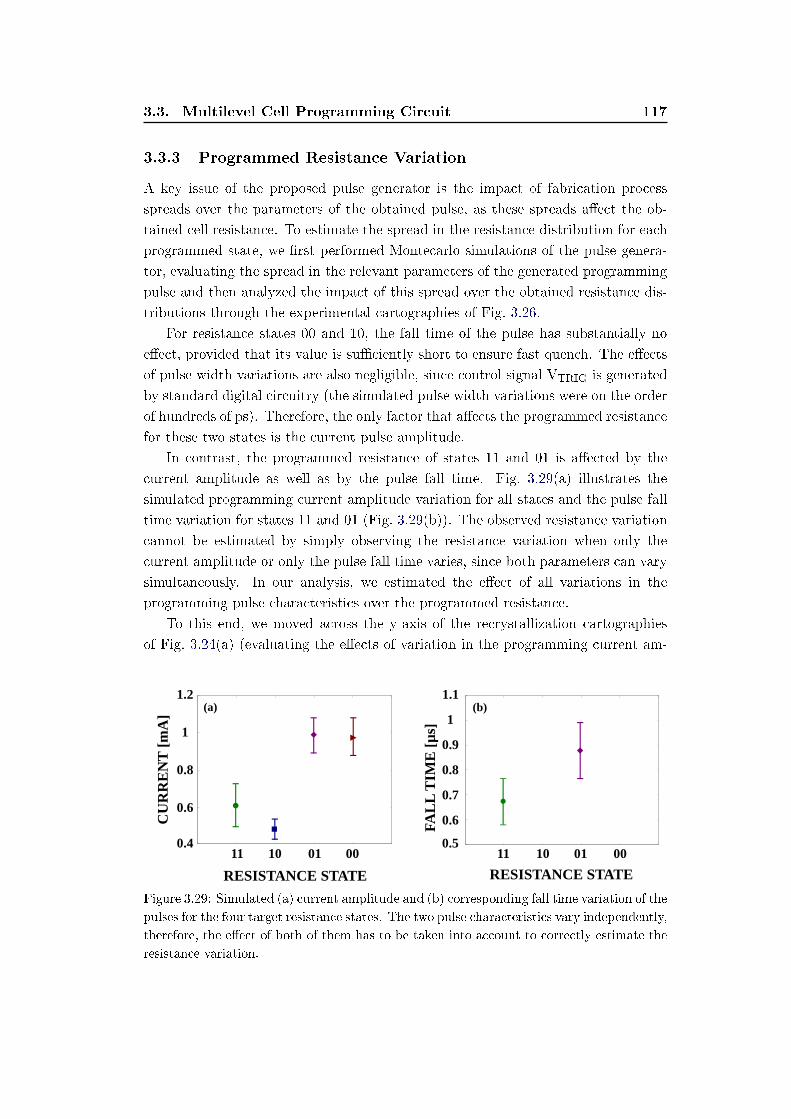
3.3. Multilevel Cell Programming Circuit 117
3.3.3 Programmed Resistance Variation
A key issue of the proposed pulse generator is the impact of fabrication process
spreads over the parameters of the obtained pulse, as these spreads aect the ob-
tained cell resistance. To estimate the spread in the resistance distribution for each
programmed state, we rst performed Montecarlo simulations of the pulse genera-
tor, evaluating the spread in the relevant parameters of the generated programming
pulse and then analyzed the impact of this spread over the obtained resistance dis-
tributions through the experimental cartographies of Fig. 3.26.
For resistance states 00 and 10, the fall time of the pulse has substantially no
eect, provided that its value is suciently short to ensure fast quench. The eects
of pulse width variations are also negligible, since control signal VTRIG is generated
by standard digital circuitry (the simulated pulse width variations were on the order
of hundreds of ps). Therefore, the only factor that aects the programmed resistance
for these two states is the current pulse amplitude.
In contrast, the programmed resistance of states 11 and 01 is aected by the
current amplitude as well as by the pulse fall time. Fig. 3.29(a) illustrates the
simulated programming current amplitude variation for all states and the pulse fall
time variation for states 11 and 01 (Fig. 3.29(b)). The observed resistance variation
cannot be estimated by simply observing the resistance variation when only the
current amplitude or only the pulse fall time varies, since both parameters can vary
simultaneously. In our analysis, we estimated the eect of all variations in the
programming pulse characteristics over the programmed resistance.
To this end, we moved across the y-axis of the recrystallization cartographies
of Fig. 3.24(a) (evaluating the eects of variation in the programming current am-
RESISTANCE STATE
00
CU
RR
EN
T [m
A]
011011
(a)
0.6
0.8
1
0.4
1.2
6
7
8
9
10
11
12
0.7
0.9
1.1(b)
1
0.8
00
FALL
TIM
E [µ
s]
011011
RESISTANCE STATE
0.6
0.5
Figure 3.29: Simulated (a) current amplitude and (b) corresponding fall time variation of the
pulses for the four target resistance states. The two pulse characteristics vary independently,
therefore, the eect of both of them has to be taken into account to correctly estimate the
resistance variation.
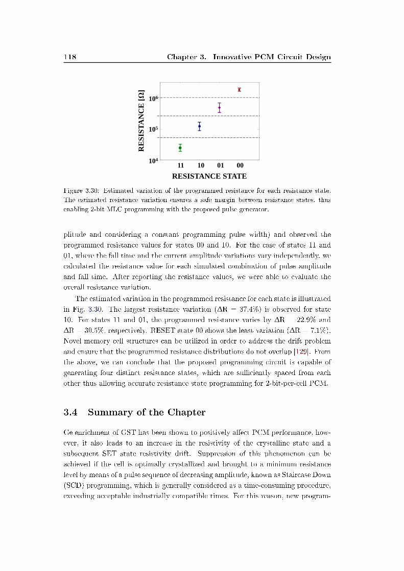
118 Chapter 3. Innovative PCM Circuit Design
00
RE
SIS
TAN
CE
[Ω
]
011011104
105
106
RESISTANCE STATE
Figure 3.30: Estimated variation of the programmed resistance for each resistance state.
The estimated resistance variation ensures a safe margin between resistance states, thus
enabling 2-bit MLC programming with the proposed pulse generator.
plitude and considering a constant programming pulse width) and observed the
programmed resistance values for states 00 and 10. For the case of states 11 and
01, where the fall time and the current amplitude variations vary independently, we
calculated the resistance value for each simulated combination of pulse amplitude
and fall time. After reporting the resistance values, we were able to evaluate the
overall resistance variation.
The estimated variation in the programmed resistance for each state is illustrated
in Fig. 3.30. The largest resistance variation (∆R = 37.4%) is observed for state
10. For states 11 and 01, the programmed resistance varies by ∆R = 22.9% and
∆R = 30.5%, respectively. RESET state 00 shows the least variation (∆R = 7.1%).
Novel memory cell structures can be utilized in order to address the drift problem
and ensure that the programmed resistance distributions do not overlap [129]. From
the above, we can conclude that the proposed programming circuit is capable of
generating four distinct resistance states, which are suciently spaced from each
other thus allowing accurate resistance state programming for 2-bit-per-cell PCM.
3.4 Summary of the Chapter
Ge enrichment of GST has been shown to positively aect PCM performance, how-
ever, it also leads to an increase in the resistivity of the crystalline state and a
subsequent SET state resistivity drift. Suppression of this phenomenon can be
achieved if the cell is optimally crystallized and brought to a minimum resistance
level by means of a pulse sequence of decreasing amplitude, known as Staircase Down
(SCD) programming, which is generally considered as a time-consuming procedure,
exceeding acceptable industrially compatible times. For this reason, new program-
3.4. Summary of the Chapter 119
ming techniques must be utilized in order to guarantee reliable programming of
memory devices, remaining compliant with industrial standards.
Among the programming techniques discussed in this Chapter, the R-SET pulse
is capable of providing an appropriate current vs. time prole to the memory cell,
enabling an optimum crystallization by accurate control of the amplitude and the
fall time of the SET programming voltage pulse. It is thus possible to bring the
cell to a low resistance value in times as short as 1 µs, targeting SET programming
of innovative PCM materials with low crystallization speed. The presented R-SET
pulse generator allows full control of the R-SET pulse characteristics and can t the
crystallization demands of a variety of materials under study, thus enabling good
crystallization of phase change materials in industrially compatible times.
An additional programming technique, capable of providing an optimum crys-
tallization to the active region of the memory cell and, therefore, minimize the
resistance distribution dispersion of the SET state has been also presented. This
technique consists in a single-pulse procedure and generates a linear temperature
prole that has been shown to lead to an optimal crystallization of the phase change
material. Two design implementations capable of generating this pulse have been
presented, both able to generate programming voltage pulses which ensure a con-
stant decrease rate of the programming temperature inside the active volume of the
cell after the pulse plateau.
Finally, the recrystallization cartographies introduced in Chapter 2 can be used
in order to provide optimal programming characteristics (pulse amplitude, width,
fall time) and ensure accurate programming of intermediate resistance states, thus
enabling the storage of multiple bits per cell. Thanks to the low crystallization
speed N-doped Ge-rich GST demonstrates, it is possible to determine the program-
ming conditions which result in resistance states of a specic value. By means of
Montecarlo simulation the spread in the relevant parameters of the generated pro-
gramming pulses was evaluated and then the impact of this spread over the obtained
resistance distributions through the experimental cartographies was analyzed. The
results of this study validate that the proposed circuit is capable of generating four
distinct resistance states, suciently spaced from each other, allowing accurate MLC
programming for 2-bit-per-cell PCM.

Chapter 4
On-Wafer Pulse Generator
Advanced memory devices necessitate programming techniques and peripheral cir-
cuitry that are inevitably complex when accurate programming is desired. The basic
programming circuit which represents one of the key items of this Thesis, has been
introduced in Chapter 3. In the present Chapter, the full design implementation
that was carried out during this study is discussed. It should be noted that the
developed on-wafer pulse generator is intended for characterization purposes, not
for use in commercial devices.
The main idea behind the followed design approach was to co-integrate memory
cells and peripheral circuitry for memory testing on the same wafer, with metal
layers 1 to 4 used for the BEOL part (circuitry) and metal layers 5 and above
dedicated to the deposition of the phase change elements, as portrayed in Fig. 4.1.
For this implementation, we used cells having a standard height (7.26 µm) and
the possibility to be vertically mirrored (ipped), in order to enable the use of
the common metal line as VDD or GND (Fig. 4.2). This way, a more compact,
rectangular physical layout can be obtained and the supply signals do not experience
any signicant voltage drop along the lines. STMicroelectronics 130 nm CMOS
FEOL + BEOL (foundry)- 4 Cu layers- 130 nm CMOS technology
Final deposition (LETI)- 1 – 2 metal layers + PCM structures- 50 nm (e-beam)/ 300 nm (DUV) technology
Figure 4.1: Metal layer schematic of BEOL layers (peripheral circuitry) and memory ele-
ments deposition (layers 5 - 6).
122 Chapter 4. On-Wafer Pulse Generator
POLYSILICONMETAL 1METAL 2METAL 3METAL 4CELL 1
CELL 2 (FLIPPED)
GND VDDMETAL 4
Figure 4.2: Layout instant. The standard-sized cells are placed in a mirrored fashion, so
that minimum space is used, thus achieving a more compact layout.
technology was used and a 25-pad scribe line was made available to provide the
input and output signals of the circuit.
Due to the diculties of generating currents externally through the automatic
characterization equipment, the approach followed was to internally generate all
the required currents. In addition, the currents that control the fall slope of the
generated SET pulse are digitally programmed by means of external voltages. This
method presents the disadvantage of potential inaccuracy of the generated currents
due to fabrication process spreads and variations in operating conditions, but, as
will be described later, is capable of generating up to eight dierent slopes for the
falling edge of the SET programming pulse, thus covering the essential cases of
pulses necessary for PCM programming.
Even though device characterization was the nal target of this design implemen-
tation, it was not possible to integrate the memory elements on top of metal layer 4
due to time-related constraints. Therefore, the eect of programming the memory
cell with the circuit presented in the previous Chapter could not be experimentally
investigated. However, in the present Chapter, we show the design that was im-
plemented and the layout of the developed circuit block. Post-layout simulations
are compared to the simulations of the schematics, demonstrating good agreement.
Finally, experimental results of the fabricated integrated circuit are presented.
4.1 Design Implementation
In order to facilitate the understanding of the circuit operation, Fig. 4.3 illustrates
the blocks taking part in pulse generation. When compared to the previous design
4.1. Design Implementation 123
TIME REFERENCE
GENERATION
COMPARISON BLOCK
LOGICBLOCK
SET PULSE CONTROL
LINEAR V SET PULSE
GENERATION
LINEAR TSET PULSE
GENERATION
MIXING BLOCK
LDO BLOCK
ADDRESS DECODER
TIME REFERENCE
CONTROL
READINGBLOCK
Figure 4.3: Block diagram of the on-wafer implementation of the R-SET pulse generator.
(Section 3.1), the conguration in Fig. 4.3 includes two additional blocks for pulse
falling edge control, i.e. blocks Time Reference Control and Set Pulse Control,
which control the slope of signal TIMEREF and that of the falling edge of the SET
pulse respectively and blocks Address Decoder and Reading Block. The Address
Decoder enables the addressing of the memory cell to be programmed, while the
Reading Block enables the read-out of a resistance by sensing the current that ows
through the resistive element when a known voltage drop is applied across it. The
current capability required to drive the load is provided by the unity-gain buer
(LDO Block) placed before the Address Decoder. The unity-gain buer and the
analog switches of the Address Decoder were sized in order to provide an output
current of up to 5 mA.
The circuit operates as follows: External digital signals SS0, SS1 and SS2 control
the fall slope of signal TIMEREF (four dierent slopes are available, each corre-
sponding to one or more SET pulse fall slopes, as will be described later). Each
combination of these digital signals allows determining a xed SET pulse fall time,
resulting in a total of eight possible fall slopes for the SET pulse. More specically,
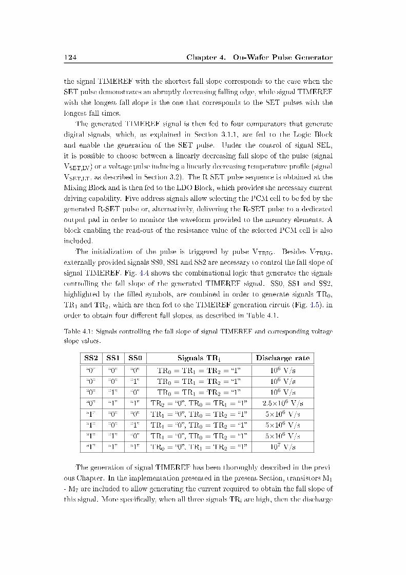
124 Chapter 4. On-Wafer Pulse Generator
the signal TIMEREF with the shortest fall slope corresponds to the case when the
SET pulse demonstrates an abruptly decreasing falling edge, while signal TIMEREF
with the longest fall slope is the one that corresponds to the SET pulses with the
longest fall times.
The generated TIMEREF signal is then fed to four comparators that generate
digital signals, which, as explained in Section 3.1.1, are fed to the Logic Block
and enable the generation of the SET pulse. Under the control of signal SEL,
it is possible to choose between a linearly decreasing fall slope of the pulse (signal
VSET,LV) or a voltage pulse inducing a linearly decreasing temperature prole (signal
VSET,LT, as described in Section 3.2). The R-SET pulse sequence is obtained at the
Mixing Block and is then fed to the LDO Block, which provides the necessary current
driving capability. Five address signals allow selecting the PCM cell to be fed by the
generated R-SET pulse or, alternatively, delivering the R-SET pulse to a dedicated
output pad in order to monitor the waveform provided to the memory elements. A
block enabling the read-out of the resistance value of the selected PCM cell is also
included.
The initialization of the pulse is triggered by pulse VTRIG. Besides VTRIG,
externally provided signals SS0, SS1 and SS2 are necessary to control the fall slope of
signal TIMEREF. Fig. 4.4 shows the combinational logic that generates the signals
controlling the fall slope of the generated TIMEREF signal. SS0, SS1 and SS2,
highlighted by the lled symbols, are combined in order to generate signals TR0,
TR1 and TR2, which are then fed to the TIMEREF generation circuit (Fig. 4.5), in
order to obtain four dierent fall slopes, as described in Table 4.1.
Table 4.1: Signals controlling the fall slope of signal TIMEREF and corresponding voltage
slope values.
SS2 SS1 SS0 Signals TRi Discharge rate
0 0 0 TR0 = TR1 = TR2 = 1 106 V/s
0 0 1 TR0 = TR1 = TR2 = 1 106 V/s
0 1 0 TR0 = TR1 = TR2 = 1 106 V/s
0 1 1 TR2 = 0, TR0 = TR1 = 1 2.5×10⁶ V/s1 0 0 TR1 = 0, TR0 = TR2 = 1 5×10⁶ V/s1 0 1 TR1 = 0, TR0 = TR2 = 1 5×10⁶ V/s1 1 0 TR1 = 0, TR0 = TR2 = 1 5×10⁶ V/s1 1 1 TR0 = 0, TR1 = TR2 = 1 107 V/s
The generation of signal TIMEREF has been thoroughly described in the previ-
ous Chapter. In the implementation presented in the present Section, transistors M1
- M7 are included to allow generating the current required to obtain the fall slope of
this signal. More specically, when all three signals TRi are high, then the discharge
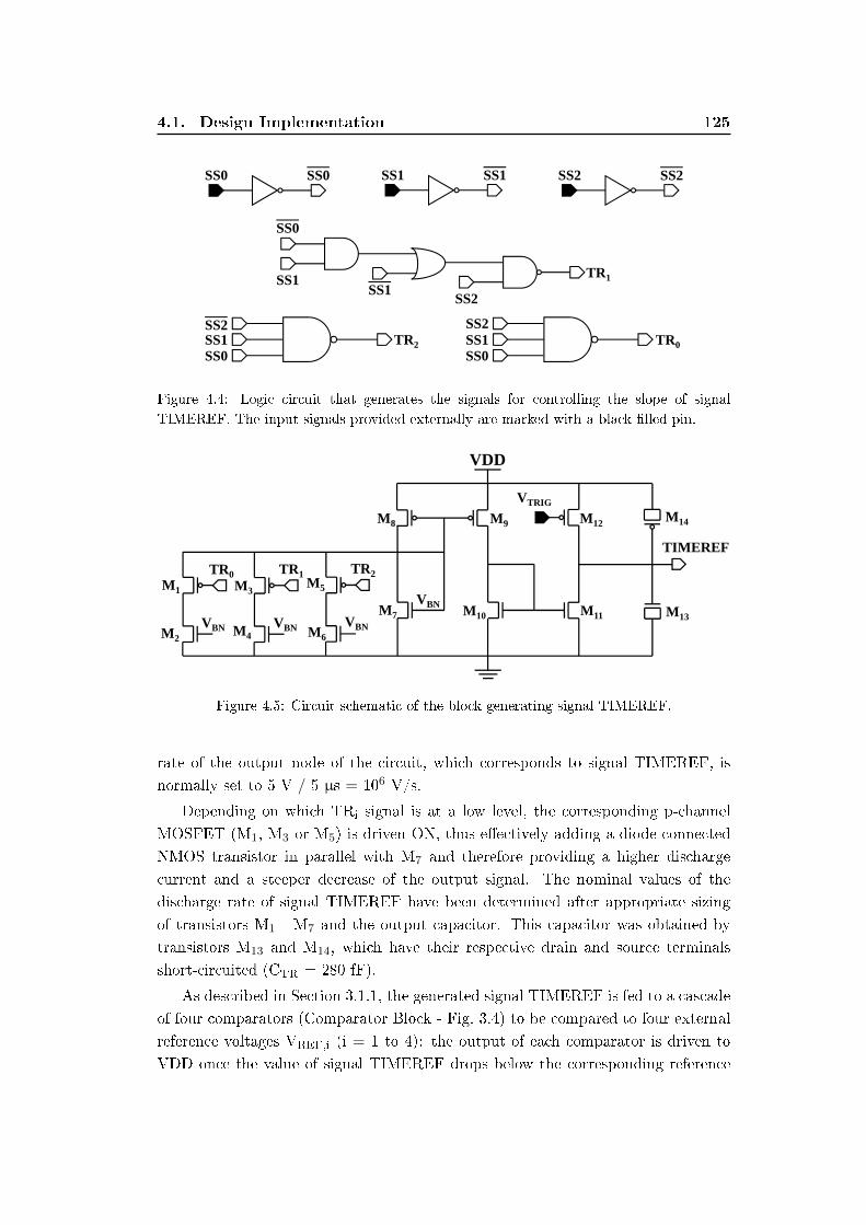
4.1. Design Implementation 125
SS0 SS0 SS2 SS2SS1 SS1
SS0
SS1SS1
SS2
TR1
SS1SS0
SS2TR2 SS1
SS0
SS2TR0
Figure 4.4: Logic circuit that generates the signals for controlling the slope of signal
TIMEREF. The input signals provided externally are marked with a black lled pin.
VDD
TIMEREF
M1
M2
VTRIG
VBN
VBNVBNVBN
M3M5
M4 M6
TR0 TR1 TR2
M7
M8 M9
M10 M11
M12
M13
M14
Figure 4.5: Circuit schematic of the block generating signal TIMEREF.
rate of the output node of the circuit, which corresponds to signal TIMEREF, is
normally set to 5 V / 5 µs = 106 V/s.
Depending on which TRi signal is at a low level, the corresponding p-channel
MOSFET (M1, M3 or M5) is driven ON, thus eectively adding a diode-connected
NMOS transistor in parallel with M7 and therefore providing a higher discharge
current and a steeper decrease of the output signal. The nominal values of the
discharge rate of signal TIMEREF have been determined after appropriate sizing
of transistors M1 - M7 and the output capacitor. This capacitor was obtained by
transistors M13 and M14, which have their respective drain and source terminals
short-circuited (CTR = 280 fF).
As described in Section 3.1.1, the generated signal TIMEREF is fed to a cascade
of four comparators (Comparator Block - Fig. 3.4) to be compared to four external
reference voltages VREF,i (i = 1 to 4): the output of each comparator is driven to
VDD once the value of signal TIMEREF drops below the corresponding reference
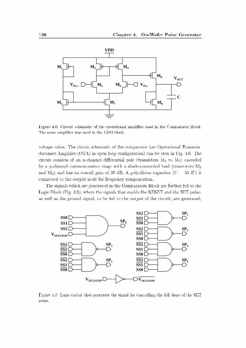
126 Chapter 4. On-Wafer Pulse Generator
VIN,+ VIN,-
VOUT
VDD
C
M1
M2
M3 M4
M6M5
M7
M8
M9
Figure 4.6: Circuit schematic of the operational amplier used in the Comparator Block.
The same amplier was used in the LDO block.
voltage value. The circuit schematic of the comparator (an Operational Transcon-
ductance Amplier (OTA) in open loop conguration) can be seen in Fig. 4.6. The
circuit consists of an n-channel dierential pair (transistors M3 to M7) cascaded
by a p-channel common-source stage with a diode-connected load (transistors M8
and M9) and has an overall gain of 30 dB. A polysilicon capacitor (C = 50 fF) is
connected to the output node for frequency compensation.
The signals which are generated in the Comparators Block are further fed to the
Logic Block (Fig. 3.5), where the signals that enable the RESET and the SET pulse,
as well as the ground signal, to be fed to the output of the circuit, are generated,
VSET,STOP VSET,STOP
SS1SS0
SS2VSET,STOP
SP0SS1SS0
SS2 SP1
SS1SS0
SS2 SP5
SS1SS0
SS2 SP3
SS1SS0
SS2 SP2
SS1SS0
SS2 SP6
SS1SS0
SS2 SP4
Figure 4.7: Logic circuit that generates the signal for controlling the fall slope of the SET
pulse.
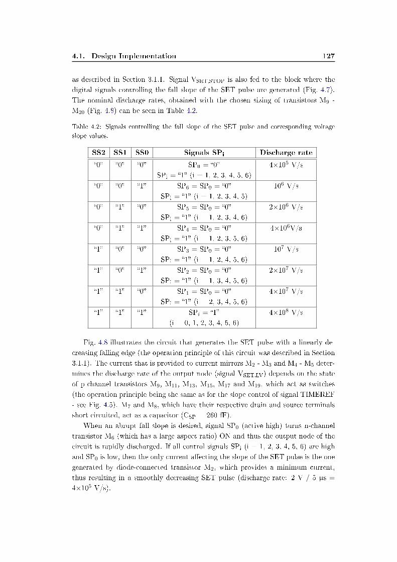
4.1. Design Implementation 127
as described in Section 3.1.1. Signal VSET,STOP is also fed to the block where the
digital signals controlling the fall slope of the SET pulse are generated (Fig. 4.7).
The nominal discharge rates, obtained with the chosen sizing of transistors M9 -
M20 (Fig. 4.8) can be seen in Table 4.2.
Table 4.2: Signals controlling the fall slope of the SET pulse and corresponding voltage
slope values.
SS2 SS1 SS0 Signals SPi Discharge rate
0 0 0 SP0 = 0
SPi = 1 (i = 1, 2, 3, 4, 5, 6)
4×10⁵ V/s
0 0 1 SP6 = SP0 = 0
SPi = 1 (i = 1, 2, 3, 4, 5)
106 V/s
0 1 0 SP5 = SP0 = 0
SPi = 1 (i = 1, 2, 3, 4, 6)
2×10⁶ V/s
0 1 1 SP4 = SP0 = 0
SPi = 1 (i = 1, 2, 3, 5, 6)
4×10⁶V/s
1 0 0 SP3 = SP0 = 0
SPi = 1 (i = 1, 2, 4, 5, 6)
107 V/s
1 0 1 SP2 = SP0 = 0
SPi = 1 (i = 1, 3, 4, 5, 6)
2×10⁷ V/s
1 1 0 SP1 = SP0 = 0
SPi = 1 (i = 2, 3, 4, 5, 6)
4×10⁷ V/s
1 1 1 SPi = 1
(i = 0, 1, 2, 3, 4, 5, 6)
4×10⁸ V/s
Fig. 4.8 illustrates the circuit that generates the SET pulse with a linearly de-
creasing falling edge (the operation principle of this circuit was described in Section
3.1.1). The current that is provided to current mirrors M2 - M3 and M4 - M5 deter-
mines the discharge rate of the output node (signal VSET,LV) depends on the state
of p-channel transistors M9, M11, M13, M15, M17 and M19, which act as switches
(the operation principle being the same as for the slope control of signal TIMEREF
- see Fig. 4.5). M7 and M8, which have their respective drain and source terminals
short-circuited, act as a capacitor (CSP = 260 fF).
When an abrupt fall slope is desired, signal SP0 (active high) turns n-channel
transistor M6 (which has a large aspect ratio) ON and thus the output node of the
circuit is rapidly discharged. If all control signals SPi (i = 1, 2, 3, 4, 5, 6) are high
and SP0 is low, then the only current aecting the slope of the SET pulse is the one
generated by diode-connected transistor M2, which provides a minimum current,
thus resulting in a smoothly decreasing SET pulse (discharge rate: 2 V / 5 µs =
4×10⁵ V/s).
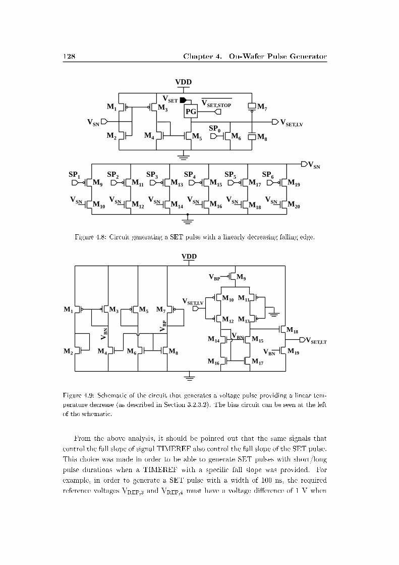
128 Chapter 4. On-Wafer Pulse Generator
M10VSNVSNVSNVSNVSN VSN
SP1
VSN
SP2 SP3 SP4 SP5 SP6
M12 M14 M16 M18 M20
M19M17M15M13M11M9
VDD
VSET,LV
M1
M4
VSET VSET,STOP
VSN
M2
M3
M5 M6
M7
M8
SP0
PG
Figure 4.8: Circuit generating a SET pulse with a linearly decreasing falling edge.
M 1
VB
N
VDD
VBP
VB
P
VBN
VBN
VSET,LV
VSET,LT
M 2
M 3
M 4
M 5
M 6
M 7
M 8
M 9
M 10 M 11
M 12 M 13
M 14 M 15
M 16 M 17
M 18
M 19
Figure 4.9: Schematic of the circuit that generates a voltage pulse providing a linear tem-
perature decrease (as described in Section 3.2.3.2). The bias circuit can be seen at the left
of the schematic.
From the above analysis, it should be pointed out that the same signals that
control the fall slope of signal TIMEREF also control the fall slope of the SET pulse.
This choice was made in order to be able to generate SET pulses with short/long
pulse durations when a TIMEREF with a specic fall slope was provided. For
example, in order to generate a SET pulse with a width of 100 ns, the required
reference voltages VREF,3 and VREF,4 must have a voltage dierence of 1 V when
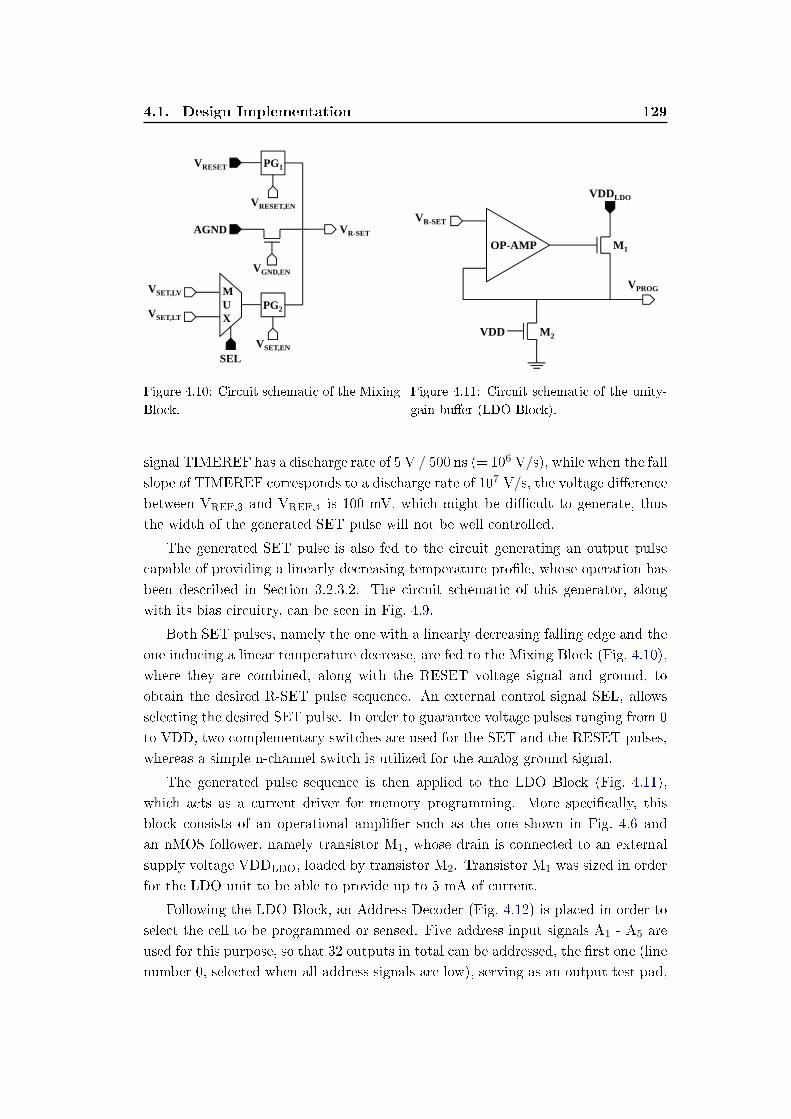
4.1. Design Implementation 129
VR-SET
VRESET
VRESET,EN
VGND,EN
PG1
AGND
VSET,EN
PG2
VSET,LV
VSET,LT
MUX
SEL
Figure 4.10: Circuit schematic of the Mixing
Block.
VDD
VDDLDO
VR-SET
OP-AMP M1
M2
VPROG
Figure 4.11: Circuit schematic of the unity-
gain buer (LDO Block).
signal TIMEREF has a discharge rate of 5 V / 500 ns (= 106 V/s), while when the fall
slope of TIMEREF corresponds to a discharge rate of 107 V/s, the voltage dierence
between VREF,3 and VREF,4 is 100 mV, which might be dicult to generate, thus
the width of the generated SET pulse will not be well controlled.
The generated SET pulse is also fed to the circuit generating an output pulse
capable of providing a linearly decreasing temperature prole, whose operation has
been described in Section 3.2.3.2. The circuit schematic of this generator, along
with its bias circuitry, can be seen in Fig. 4.9.
Both SET pulses, namely the one with a linearly decreasing falling edge and the
one inducing a linear temperature decrease, are fed to the Mixing Block (Fig. 4.10),
where they are combined, along with the RESET voltage signal and ground, to
obtain the desired R-SET pulse sequence. An external control signal SEL, allows
selecting the desired SET pulse. In order to guarantee voltage pulses ranging from 0
to VDD, two complementary switches are used for the SET and the RESET pulses,
whereas a simple n-channel switch is utilized for the analog ground signal.
The generated pulse sequence is then applied to the LDO Block (Fig. 4.11),
which acts as a current driver for memory programming. More specically, this
block consists of an operational amplier such as the one shown in Fig. 4.6 and
an nMOS follower, namely transistor M1, whose drain is connected to an external
supply voltage VDDLDO, loaded by transistor M2. Transistor M1 was sized in order
for the LDO unit to be able to provide up to 5 mA of current.
Following the LDO Block, an Address Decoder (Fig. 4.12) is placed in order to
select the cell to be programmed or sensed. Five address input signals A1 - A5 are
used for this purpose, so that 32 outputs in total can be addressed, the rst one (line
number 0, selected when all address signals are low), serving as an output test pad,
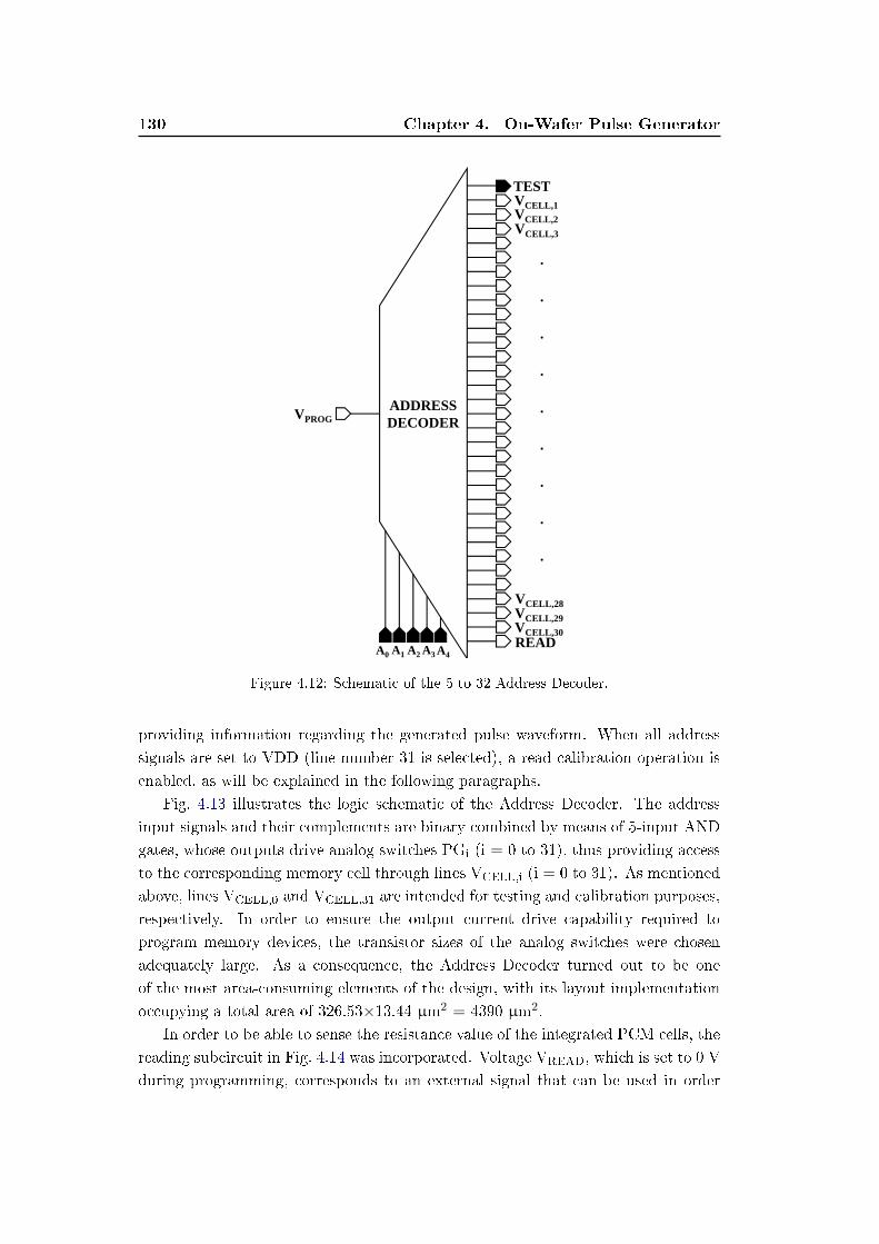
130 Chapter 4. On-Wafer Pulse Generator
VPROGADDRESS DECODER
VCELL,1VCELL,2VCELL,3
VCELL,30
VCELL,29
VCELL,28
READ
TEST
..
..
..
..
.
A0 A1 A2A3A4
Figure 4.12: Schematic of the 5 to 32 Address Decoder.
providing information regarding the generated pulse waveform. When all address
signals are set to VDD (line number 31 is selected), a read calibration operation is
enabled, as will be explained in the following paragraphs.
Fig. 4.13 illustrates the logic schematic of the Address Decoder. The address
input signals and their complements are binary combined by means of 5-input AND
gates, whose outputs drive analog switches PGi (i = 0 to 31), thus providing access
to the corresponding memory cell through lines VCELL,i (i = 0 to 31). As mentioned
above, lines VCELL,0 and VCELL,31 are intended for testing and calibration purposes,
respectively. In order to ensure the output current drive capability required to
program memory devices, the transistor sizes of the analog switches were chosen
adequately large. As a consequence, the Address Decoder turned out to be one
of the most area-consuming elements of the design, with its layout implementation
occupying a total area of 326.53×13.44 µm2 = 4390 µm2.
In order to be able to sense the resistance value of the integrated PCM cells, the
reading subcircuit in Fig. 4.14 was incorporated. Voltage VREAD, which is set to 0 V
during programming, corresponds to an external signal that can be used in order
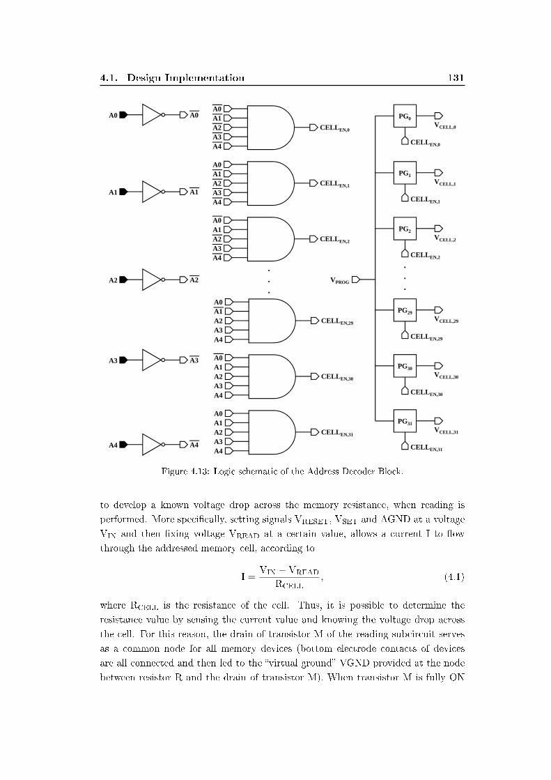
4.1. Design Implementation 131
CELLEN,0
A0A1A2A3A4
CELLEN,1
A0A1A2A3A4
CELLEN,2
A0A1A2A3A4
A0A0
A2A2
A1A1
A3A3
A4A4
CELLEN,31
A0A1A2A3A4
CELLEN,30
A0A1A2A3A4
CELLEN,29
A0A1A2A3A4
.
.
.
PG0
PG1
PG2
PG29
PG30
PG31
CELLEN,2
CELLEN,29
CELLEN,30
CELLEN,31
CELLEN,0
CELLEN,1
VPROG
VCELL,0
VCELL,1
VCELL,2
VCELL,29
VCELL,30
VCELL,31
.
.
.
Figure 4.13: Logic schematic of the Address Decoder Block.
to develop a known voltage drop across the memory resistance, when reading is
performed. More specically, setting signals VRESET, VSET and AGND at a voltage
VIN and then xing voltage VREAD at a certain value, allows a current I to ow
through the addressed memory cell, according to
I =VIN −VREAD
RCELL, (4.1)
where RCELL is the resistance of the cell. Thus, it is possible to determine the
resistance value by sensing the current value and knowing the voltage drop across
the cell. For this reason, the drain of transistor M of the reading subcircuit serves
as a common node for all memory devices (bottom electrode contacts of devices
are all connected and then led to the virtual ground VGND provided at the node
between resistor R and the drain of transistor M). When transistor M is fully ON
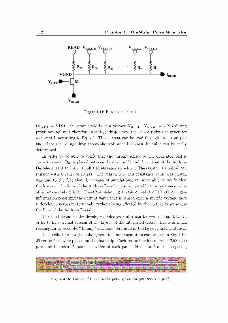
132 Chapter 4. On-Wafer Pulse Generator
VG,FT
READ
VREAD
R31
IREAD
M
R30 R29 R2 R1
VGND
VCELL,2 VCELL,1VCELL,30 VCELL,29
. . .
Figure 4.14: Reading subcircuit.
(VG,FT = VDD), the drain node is at a voltage VREAD (VREAD = GND during
programming) and, therefore, a voltage drop across the sensed resistance generates
a current I, according to Eq. 4.1. This current can be read through an output pad
and, since the voltage drop across the resistance is known, its value can be easily
determined.
In order to be able to verify that the current sensed at the dedicated pad is
correct, resistor R31 is placed between the drain of M and the output of the Address
Decoder that is active when all address signals are high. The resistor is a polysilicon
resistor with a value of 10 kΩ. The reason why this resistance value was chosen
was due to the fact that, by means of simulations, we were able to verify that
the losses at the lines of the Address Decoder are comparable to a resistance value
of approximately 2 kΩ. Therefore, selecting a resistor value of 10 kΩ can give
information regarding the current value that is sensed once a specic voltage drop
is developed across its terminals, without being aected by the voltage losses across
the lines of the Address Decoder.
The nal layout of the developed pulse generator can be seen in Fig. 4.15. In
order to have a nal version of the layout of the integrated circuit that is as much
rectangular as possible, dummy elements were used in the layout implementation.
The scribe lines for the pulse generation implementation can be seen in Fig. 4.16.
25 scribe lines were placed on the nal chip. Each scribe line has a size of 2500x200
µm2 and includes 25 pads. The size of each pad is 50x90 µm2 and the spacing
Figure 4.15: Layout of the on-wafer pulse generator (381.88×33.5 µm2).
4.1. Design Implementation 133
Figure 4.16: Scribe lines of the on-wafer pulse generator.
between them is 30 µm for a pitch of 80 µm. An appropriately designated probe
card was used during testing in order to access the pads and provide the supplies
and the signals necessary for circuit operation and sensing the generated signal. The
pad numbering and the corresponding signals/supplies are seen in Table 4.3.
Table 4.3: Pad numbering and corresponding signals/supplies.
Pad no. Signal Pad no. Signal
1 VDD 14 VRESET
2 VDDIO 15 VDDLDO
3 VTRIG 16 VG,FT
4 SS0 17 VREAD
5 SS1 18 A4
6 SS2 19 A3
7 SEL 20 A2
8 VREF,1 21 A1
9 VREF,2 22 A0
10 VREF,3 23 IREAD11 VREF,4 24 TESTPAD
12 VSET 25 GND
13 AGND
The classication of the signals/supplied provided through the pads can be seen
in Fig. 4.17. In addition to the signals that have been represented above in the circuit
schematics, there are three pads for the supplies, namely the ground (GND) and the
power supplies for the circuit and the circuit input/output (I/O) circuitry (VDD
and VDDIO, respectively). The I/O circuitry mainly concerns input digital buers
necessary for the propagation of digital signals as well as the diodes protecting from
undesired electrostatic discharges and overstresses.
The layout of one single scribe line, where the pulse generator module is high-
lighted in the area within the white border, can be seen in Fig. 18. The layout of
the pad array was already available during the layout process of the circuit. In order
134 Chapter 4. On-Wafer Pulse Generator
Figure 4.17: Classication of signals for the 25 pads. The size and the pitch of the pads
can be seen in the bottom right corner of the Figure.
to provide digital signals without losses to the logic part of the circuit, digital input
buers were used, for which a dedicated VDDIO pad was utilized. The connection
of the pads to the internal metal wires was performed by means of wide lines of
metals 4 and 3.
Figure 4.18: Layout of one scribe line (metal 4). The pulse generator can be seen in the
highlighted white rectangle.
4.2 Post-Layout Simulations
After completing the layout and successfully running Design Rules Check (DRC) and
Layout versus Schematic (LVS) controls, post-layout simulations were carried out to
validate the design, observing the dierences with respect to schematic simulation
results and estimating how these dierences may aect the nal fabricated circuit.
As far as the post-layout simulations of signal TIMEREF are concerned, we need
to point out that, even though the size of the transistors congured as capacitors
was chosen carefully in order to achieve the exact value of discharge rate mentioned
in Table 4.1, post-layout simulation results (Fig. 4.19) are slightly dierent than ex-
pected. More specically, the only case where the desired discharge rate is achieved,
is the case when signal TR0 (purple line in Fig. 4.19) is low, which corresponds to
the most abrupt fall slope. The higher discharge rate that is observed for the case
when signal TR1 or signal TR2 is low, as well as when all signals TRi are high,
results in a slight time shift for the logic signals provided and generated by the
Logic Block. Since the signals generated by the Logic Block control the width of
the generated SET and RESET pulses, a time shift in these signals will result in a
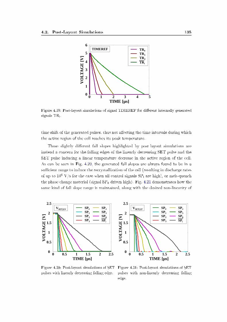
4.2. Post-Layout Simulations 135
VO
LTA
GE
[V]
1 2TIME [µs]
30 4 5
TIMEREF
0
1
2
3
4
5
6TR0
TR1TR2
TR i
Figure 4.19: Post-layout simulations of signal TIMEREF for dierent internally generated
signals TRi.
time shift of the generated pulses, thus not aecting the time intervals during which
the active region of the cell reaches its peak temperature.
These slightly dierent fall slopes highlighted by post-layout simulations are
instead a concern for the falling edges of the linearly decreasing SET pulse and the
SET pulse inducing a linear temperature decrease in the active region of the cell.
As can be seen in Fig. 4.20, the generated fall slopes are always found to be in a
sucient range to induce the recrystallization of the cell (resulting in discharge rates
of up to 106 V/s for the case when all control signals SPi are high), or melt-quench
the phase change material (signal SP0 driven high). Fig. 4.21 demonstrates how the
same kind of fall slope range is maintained, along with the desired non-linearity of
VO
LTA
GE
[V]
0 0.5 1 1.5 2 2.50.5 1TIME [µs]
1.50 2 2.5
VSET,LV
0
0.5
1
1.5
2
2.5SP4
SP5SP6
SPi
SP0
SP1SP2SP3
Figure 4.20: Post-layout simulations of SET
pulses with linearly decreasing falling edge.
VO
LTA
GE
[V]
0.5 1TIME [µs]
1.50 2 2.5
VSET,LT
0
0.5
1
1.5
2
2.5SP4
SP5SP6
SPi
SP0
SP1SP2SP3
Figure 4.21: Post-layout simulations of SET
pulses with non-linearly decreasing falling
edge.
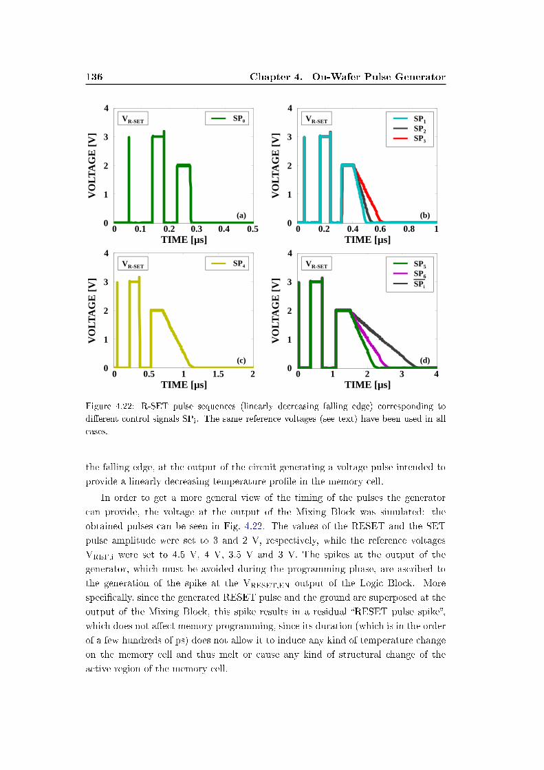
136 Chapter 4. On-Wafer Pulse Generator
0 1 2 3 4 5
VO
LTA
GE
[V]
0.1 0.2TIME [µs]
0.30 0.40
1
2
3
4SP0
0.5
VR-SET
(a)
0 0.2 0.4 0.6 0.8 1
VO
LTA
GE
[V]
0.2 0.4TIME [µs]
0.60 10
1
2
3
4
0.8
SP1SP2SP3
VR-SET
(b)
0 0.5 1 1.5 2
VO
LTA
GE
[V]
0.5 1TIME [µs]
1.50 20
1
2
3
4SP4VR-SET
(c)
0 1 2 3 4
VO
LTA
GE
[V]
1 2TIME [µs]
30 4
VR-SET
0
1
2
3
SP5SP6
SPi
4
(d)
Figure 4.22: R-SET pulse sequences (linearly decreasing falling edge) corresponding to
dierent control signals SPi. The same reference voltages (see text) have been used in all
cases.
the falling edge, at the output of the circuit generating a voltage pulse intended to
provide a linearly decreasing temperature prole in the memory cell.
In order to get a more general view of the timing of the pulses the generator
can provide, the voltage at the output of the Mixing Block was simulated: the
obtained pulses can be seen in Fig. 4.22. The values of the RESET and the SET
pulse amplitude were set to 3 and 2 V, respectively, while the reference voltages
VREF,i were set to 4.5 V, 4 V, 3.5 V and 3 V. The spikes at the output of the
generator, which must be avoided during the programming phase, are ascribed to
the generation of the spike at the VRESET,EN output of the Logic Block. More
specically, since the generated RESET pulse and the ground are superposed at the
output of the Mixing Block, this spike results in a residual RESET pulse spike,
which does not aect memory programming, since its duration (which is in the order
of a few hundreds of ps) does not allow it to induce any kind of temperature change
on the memory cell and thus melt or cause any kind of structural change of the
active region of the memory cell.
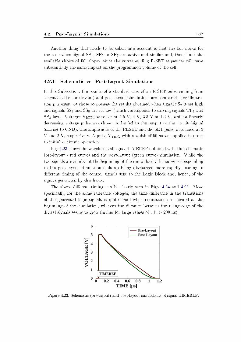
4.2. Post-Layout Simulations 137
Another thing that needs to be taken into account is that the fall slopes for
the case when signal SP1, SP2 or SP3 are active and similar and, thus, limit the
available choice of fall slopes, since the corresponding R-SET sequences will have
substantially the same impact on the programmed volume of the cell.
4.2.1 Schematic vs. Post-Layout Simulations
In this Subsection, the results of a standard case of an R-SET pulse coming from
schematic (i.e. pre-layout) and post-layout simulations are compared. For illustra-
tion purposes, we chose to present the results obtained when signal SS2 is set high
and signals SS1 and SS0 are set low (which corresponds to driving signals TR1 and
SP3 low). Voltages VREF,i were set at 4.5 V, 4 V, 3.5 V and 3 V, while a linearly
decreasing voltage pulse was chosen to be fed to the output of the circuit (signal
SEL set to GND). The amplitudes of the RESET and the SET pulse were xed at 3
V and 2 V, respectively. A pulse VTRIG with a width of 50 ns was applied in order
to initialize circuit operation.
Fig. 4.23 shows the waveforms of signal TIMEREF obtained with the schematic
(pre-layout - red curve) and the post-layout (green curve) simulation. While the
two signals are similar at the beginning of the ramp-down, the curve corresponding
to the post-layout simulation ends up being discharged more rapidly, leading to
dierent timing of the control signals sent to the Logic Block and, hence, of the
signals generated by this block.
The above dierent timing can be clearly seen in Figs. 4.24 and 4.25. More
specically, for the same reference voltages, the time dierence in the transitions
of the generated logic signals is quite small when transitions are located at the
beginning of the simulation, whereas the distance between the rising edge of the
digital signals seems to grow further for large values of t (t > 200 ns).
VO
LTA
GE
[V]
0.2 0.4 0.6TIME [µs]
0.80 1 1.20
1
2
3
4
5
6
TIMEREF
Pre-LayoutPost-Layout
Figure 4.23: Schematic (pre-layout) and post-layout simulations of signal TIMEREF.
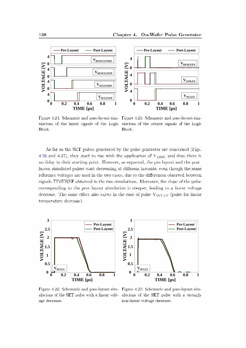
138 Chapter 4. On-Wafer Pulse Generator
TIME [µs]0.2 0.4 0.6 0.80 10 0.2 0.4 0.6 0.8 1
0
2
4
6
0
2
4
6
0 0.2 0.4 0.6 0.8 10
2
4
60
2
4
6
Pre-Layout Post-Layout
0
4
4
0
4
0
4
0
VO
LTA
GE
[V]
VRESET,START
VRESET,STOP
VSET,STOP
VSET,START
Figure 4.24: Schematic and post-layout sim-
ulations of the input signals of the Logic
Block.
0 0.2 0.4 0.6 0.8 1
VO
LTA
GE
[V]
4
TIME [µs]0.2 0.4 0.6 0.80 1
4
4
0
0
0
Pre-Layout Post-Layout
VSET,EN
VGND,EN
VRESET,EN
Figure 4.25: Schematic and post-layout sim-
ulations of the output signals of the Logic
Block.
As far as the SET pulses generated by the pulse generator are concerned (Figs.
4.26 and 4.27), they start to rise with the application of VTRIG and thus there is
no delay in their starting point. However, as expected, the pre-layout and the post-
layout simulated pulses start decreasing at dierent instants, even though the same
reference voltages are used in the two cases, due to the dierences observed between
signals TIMEREF obtained in the two simulations. Moreover, the slope of the pulse
corresponding to the post-layout simulation is steeper, leading to a faster voltage
decrease. The same eect also exists in the case of pulse VSET,LT (pulse for linear
temperature decrease).
0 0.2 0.4 0.6 0.8 1
VO
LTA
GE
[V]
0.2 0.4 0.6TIME [µs]
0.80 1
0.5
2.5
1.5
1
2
3
0
Pre-LayoutPost-Layout
VSET,LV
Figure 4.26: Schematic and post-layout sim-
ulations of the SET pulse with a linear volt-
age decrease.
VO
LTA
GE
[V]
TIME [µs]
00.2 0.4 0.6 0.80 1
Pre-LayoutPost-Layout
VSET,LT
0.5
2.5
1.5
1
2
3
Figure 4.27: Schematic and post-layout sim-
ulations of the SET pulse with a strongly
non-linear voltage decrease.
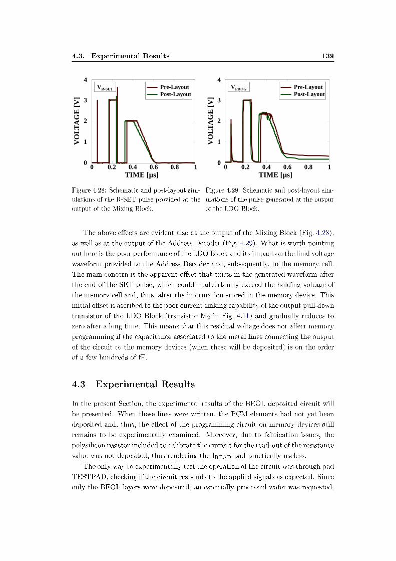
4.3. Experimental Results 139
Pre-LayoutPost-Layout
VR-SET
VO
LTA
GE
[V]
TIME [µs]
0
1
2
3
4
0.2 0.4 0.6 0.80 1
Figure 4.28: Schematic and post-layout sim-
ulations of the R-SET pulse provided at the
output of the Mixing Block.V
OLT
AG
E [V
]
TIME [µs]
0
1
2
3
4
0.2 0.4 0.6 0.80 1
Pre-LayoutPost-Layout
VPROG
Figure 4.29: Schematic and post-layout sim-
ulations of the pulse generated at the output
of the LDO Block.
The above eects are evident also at the output of the Mixing Block (Fig. 4.28),
as well as at the output of the Address Decoder (Fig. 4.29). What is worth pointing
out here is the poor performance of the LDO Block and its impact on the nal voltage
waveform provided to the Address Decoder and, subsequently, to the memory cell.
The main concern is the apparent oset that exists in the generated waveform after
the end of the SET pulse, which could inadvertently exceed the holding voltage of
the memory cell and, thus, alter the information stored in the memory device. This
initial oset is ascribed to the poor current sinking capability of the output pull-down
transistor of the LDO Block (transistor M2 in Fig. 4.11) and gradually reduces to
zero after a long time. This means that this residual voltage does not aect memory
programming if the capacitance associated to the metal lines connecting the output
of the circuit to the memory devices (when these will be deposited) is on the order
of a few hundreds of fF.
4.3 Experimental Results
In the present Section, the experimental results of the BEOL deposited circuit will
be presented. When these lines were written, the PCM elements had not yet been
deposited and, thus, the eect of the programming circuit on memory devices still
remains to be experimentally examined. Moreover, due to fabrication issues, the
polysilicon resistor included to calibrate the current for the read-out of the resistance
value was not deposited, thus rendering the IREAD pad practically useless.
The only way to experimentally test the operation of the circuit was through pad
TESTPAD, checking if the circuit responds to the applied signals as expected. Since
only the BEOL layers were deposited, an especially processed wafer was requested,
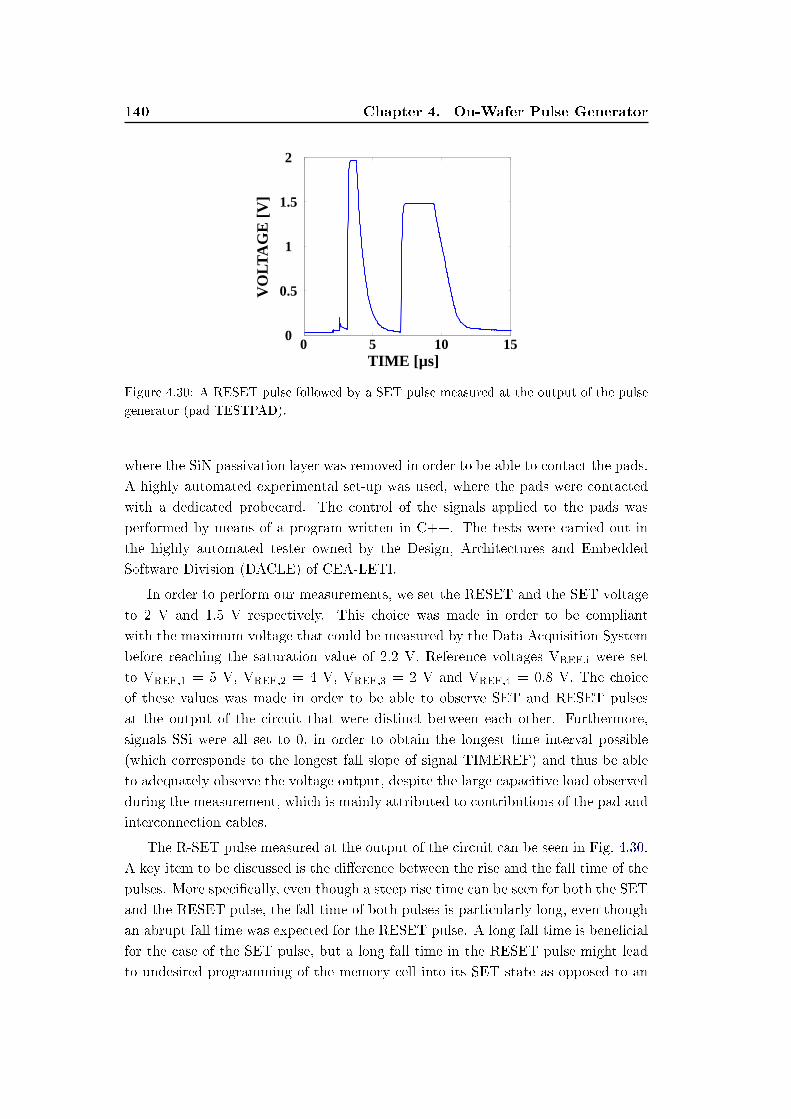
140 Chapter 4. On-Wafer Pulse Generator
0 0.5 1 1.5
VO
LTA
GE
[V]
TIME [µs]
0
0.5
1
1.5
2
5 10 150
Figure 4.30: A RESET pulse followed by a SET pulse measured at the output of the pulse
generator (pad TESTPAD).
where the SiN passivation layer was removed in order to be able to contact the pads.
A highly automated experimental set-up was used, where the pads were contacted
with a dedicated probecard. The control of the signals applied to the pads was
performed by means of a program written in C++. The tests were carried out in
the highly automated tester owned by the Design, Architectures and Embedded
Software Division (DACLE) of CEA-LETI.
In order to perform our measurements, we set the RESET and the SET voltage
to 2 V and 1.5 V respectively. This choice was made in order to be compliant
with the maximum voltage that could be measured by the Data Acquisition System
before reaching the saturation value of 2.2 V. Reference voltages VREF,i were set
to VREF,1 = 5 V, VREF,2 = 4 V, VREF,3 = 2 V and VREF,4 = 0.8 V. The choice
of these values was made in order to be able to observe SET and RESET pulses
at the output of the circuit that were distinct between each other. Furthermore,
signals SSi were all set to 0, in order to obtain the longest time interval possible
(which corresponds to the longest fall slope of signal TIMEREF) and thus be able
to adequately observe the voltage output, despite the large capacitive load observed
during the measurement, which is mainly attributed to contributions of the pad and
interconnection cables.
The R-SET pulse measured at the output of the circuit can be seen in Fig. 4.30.
A key item to be discussed is the dierence between the rise and the fall time of the
pulses. More specically, even though a steep rise time can be seen for both the SET
and the RESET pulse, the fall time of both pulses is particularly long, even though
an abrupt fall time was expected for the RESET pulse. A long fall time is benecial
for the case of the SET pulse, but a long fall time in the RESET pulse might lead
to undesired programming of the memory cell into its SET state as opposed to an
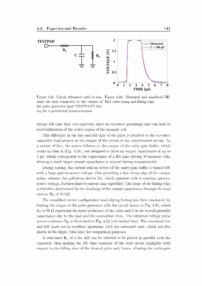
4.3. Experimental Results 141
C RL
Rs
TESTPAD
Figure 4.31: Circuit schematic used to sim-
ulate the load connected to the output of
the pulse generator (pad TESTPAD) dur-
ing the experimental characterization.V
OLT
AG
E [V
]
TIME [µs]
0
0.5
1
1.5
2
2 3 80
. . .
1 4 5 6 7
MeasuredC = 200 pF
Figure 4.32: Measured and simulated RE-
SET pulse rising and falling edge.
abrupt fall time that was expected, since an excessive quenching time can lead to
recrystallization of the active region of the memory cell.
This dierence in the rise and fall time of the pulse is ascribed to the excessive
capacitive load present at the output of the circuit in the experimental set-up. As
a matter of fact, the source follower at the output of the unity-gain buer, which
works in class A (Fig. 4.11), was designed to drive an output capacitance of up to
5 pF, which corresponds to the capacitance of a Bit Line driving 30 memory cells,
whereas a much larger output capacitance is present during measurements.
During testing, the output pull-up device of the unity-gain buer is turned ON
with a large gate-to-source voltage, thus providing a fast rising edge of the output
pulse, whereas the pull-down device M2, which operates with a constant gate-to-
source voltage, features limited current sink capability. The slope of the falling edge
is therefore determined by the discharge of the output capacitance through the load
resistor RL of 10 kΩ.
The simplied circuit conguration used during testing was then simulated, by
loading the output of the pulse generator with the circuit shown in Fig. 4.31, where
RS = 50 Ω represents the series resistance of the cable and C is the overall parasitic
capacitance due to the pad and the connection lines. The obtained voltage pulse
across resistance RL is illustrated in Fig. 4.32 (red dashed line). The simulated rise
and fall times are in excellent agreement with the measured ones, which are also
shown in the gure (blue line) for comparison purposes.
A resistance RL of a few kΩ can be selected to be placed in parallel with the
capacitor, thus making the RC time constant of the load circuit negligible with
respect to the falling time of the desired pulse and, hence, allowing the unity-gain
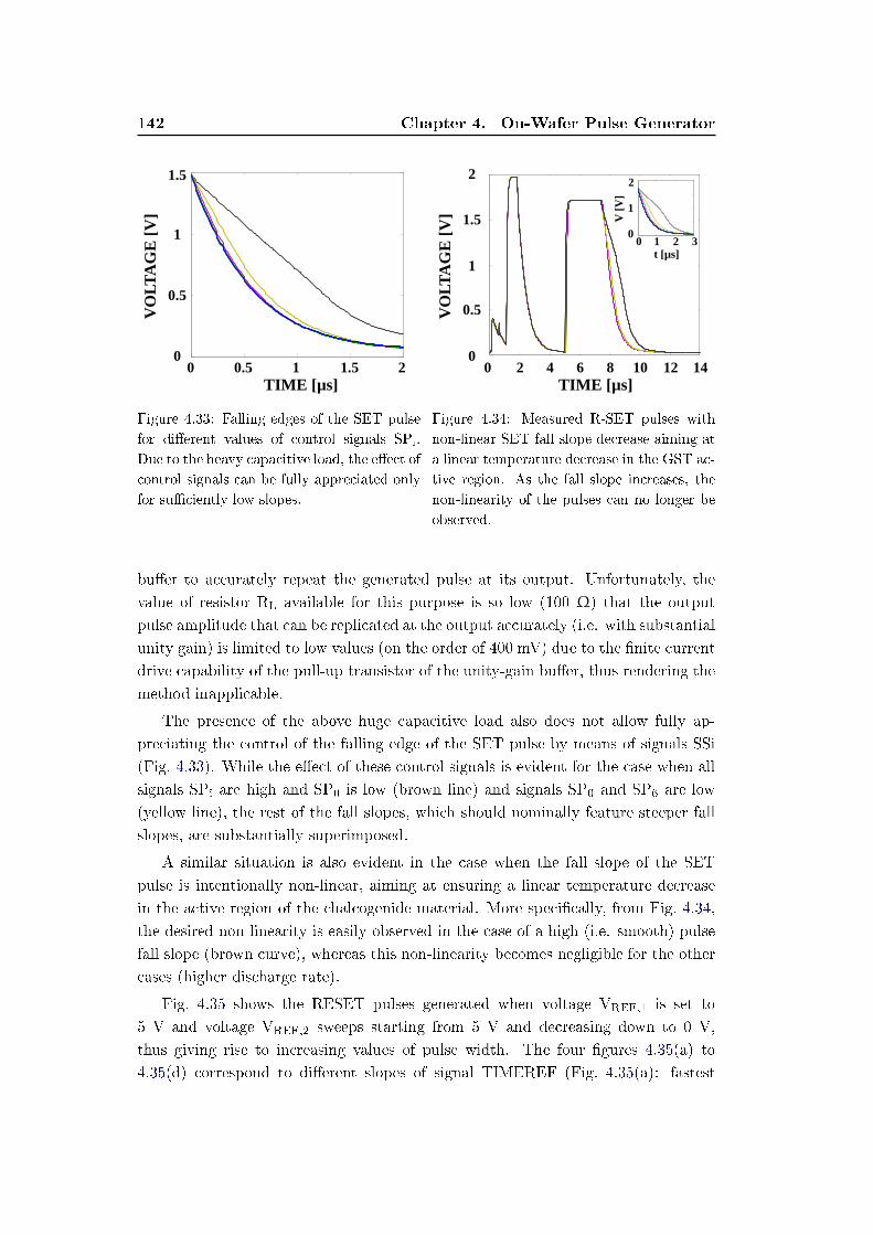
142 Chapter 4. On-Wafer Pulse Generator
VO
LTA
GE
[V]
TIME [µs]
0
0.5
1
1.5
1.510 0.5 2
Figure 4.33: Falling edges of the SET pulse
for dierent values of control signals SPi.
Due to the heavy capacitive load, the eect of
control signals can be fully appreciated only
for suciently low slopes.
2 4 6 8 10 12 14 160
0.5
1
1.5
2
VO
LTA
GE
[V]
TIME [µs]
0
0.5
1
1.5
2
420 146 8 10 12
2
00
1
1 2 3
V [V
]
t [µs]
Figure 4.34: Measured R-SET pulses with
non-linear SET fall slope decrease aiming at
a linear temperature decrease in the GST ac-
tive region. As the fall slope increases, the
non-linearity of the pulses can no longer be
observed.
buer to accurately repeat the generated pulse at its output. Unfortunately, the
value of resistor RL available for this purpose is so low (100 Ω) that the output
pulse amplitude that can be replicated at the output accurately (i.e. with substantial
unity gain) is limited to low values (on the order of 400 mV) due to the nite current
drive capability of the pull-up transistor of the unity-gain buer, thus rendering the
method inapplicable.
The presence of the above huge capacitive load also does not allow fully ap-
preciating the control of the falling edge of the SET pulse by means of signals SSi
(Fig. 4.33). While the eect of these control signals is evident for the case when all
signals SPi are high and SP0 is low (brown line) and signals SP0 and SP6 are low
(yellow line), the rest of the fall slopes, which should nominally feature steeper fall
slopes, are substantially superimposed.
A similar situation is also evident in the case when the fall slope of the SET
pulse is intentionally non-linear, aiming at ensuring a linear temperature decrease
in the active region of the chalcogenide material. More specically, from Fig. 4.34,
the desired non-linearity is easily observed in the case of a high (i.e. smooth) pulse
fall slope (brown curve), whereas this non-linearity becomes negligible for the other
cases (higher discharge rate).
Fig. 4.35 shows the RESET pulses generated when voltage VREF,1 is set to
5 V and voltage VREF,2 sweeps starting from 5 V and decreasing down to 0 V,
thus giving rise to increasing values of pulse width. The four gures 4.35(a) to
4.35(d) correspond to dierent slopes of signal TIMEREF (Fig. 4.35(a): fastest
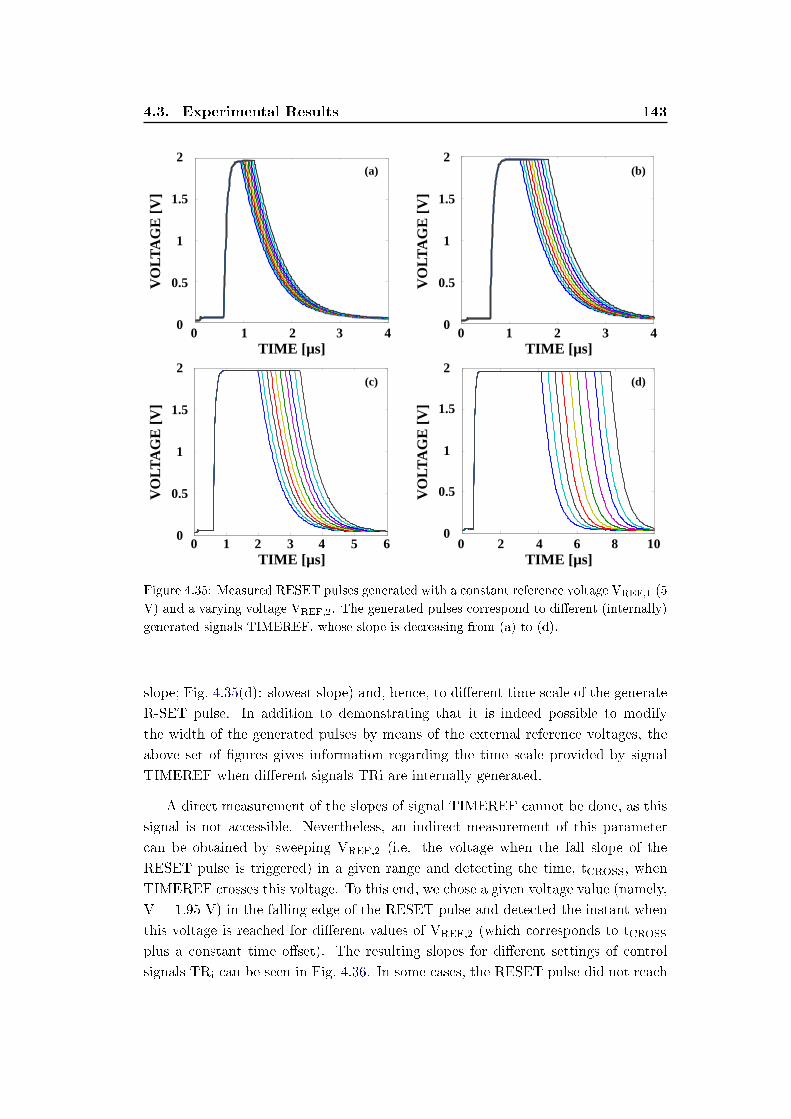
4.3. Experimental Results 143
2 3 4 5 6
VO
LTA
GE
[V]
TIME [µs]
0
0.5
1
1.5
2
1 3 40 2
(a)
VO
LTA
GE
[V]
TIME [µs]
0
0.5
1
1.5
2
1 3 40 2
(b)
2 3 4 5 6 7 8
VO
LTA
GE
[V]
TIME [µs]
0
0.5
1
1.5
2
1 3 40 2 5 6
(c)
VO
LTA
GE
[V]
TIME [µs]
0
0.5
1
1.5
2
640 2 8 10
(d)
Figure 4.35: Measured RESET pulses generated with a constant reference voltage VREF,1 (5
V) and a varying voltage VREF,2. The generated pulses correspond to dierent (internally)
generated signals TIMEREF, whose slope is decreasing from (a) to (d).
slope; Fig. 4.35(d): slowest slope) and, hence, to dierent time scale of the generate
R-SET pulse. In addition to demonstrating that it is indeed possible to modify
the width of the generated pulses by means of the external reference voltages, the
above set of gures gives information regarding the time scale provided by signal
TIMEREF when dierent signals TRi are internally generated.
A direct measurement of the slopes of signal TIMEREF cannot be done, as this
signal is not accessible. Nevertheless, an indirect measurement of this parameter
can be obtained by sweeping VREF,2 (i.e. the voltage when the fall slope of the
RESET pulse is triggered) in a given range and detecting the time, tCROSS, when
TIMEREF crosses this voltage. To this end, we chose a given voltage value (namely,
V = 1.95 V) in the falling edge of the RESET pulse and detected the instant when
this voltage is reached for dierent values of VREF,2 (which corresponds to tCROSSplus a constant time oset). The resulting slopes for dierent settings of control
signals TRi can be seen in Fig. 4.36. In some cases, the RESET pulse did not reach
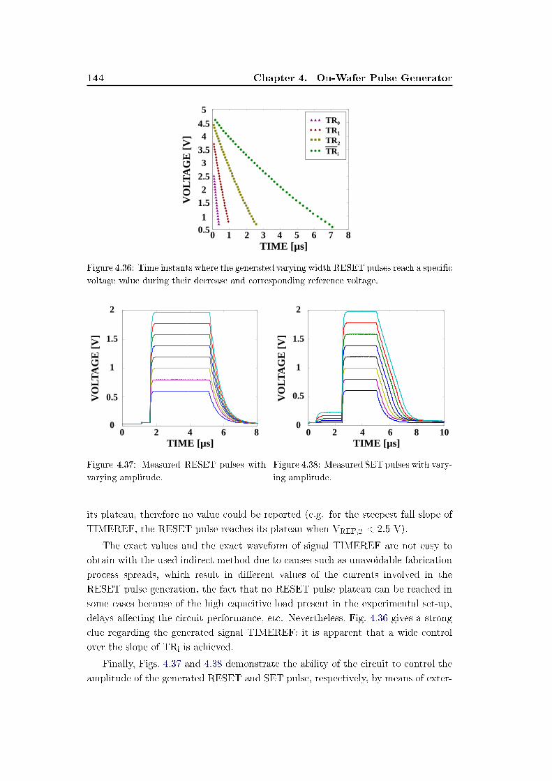
144 Chapter 4. On-Wafer Pulse Generator
VO
LTA
GE
[V]
TIME [µs]
0.51
1.5
5
320 1 84 6 75
22.53
3.54
4.5 TR0
TR1TR2
TR i
Figure 4.36: Time instants where the generated varying width RESET pulses reach a specic
voltage value during their decrease and corresponding reference voltage.
VO
LTA
GE
[V]
TIME [µs]
0
0.5
1
1.5
2
640 2 8
Figure 4.37: Measured RESET pulses with
varying amplitude.
2 4 6 8 10 12
VO
LTA
GE
[V]
TIME [µs]
0
0.5
1
1.5
2
640 2 8 10
Figure 4.38: Measured SET pulses with vary-
ing amplitude.
its plateau, therefore no value could be reported (e.g. for the steepest fall slope of
TIMEREF, the RESET pulse reaches its plateau when VREF,2 < 2.5 V).
The exact values and the exact waveform of signal TIMEREF are not easy to
obtain with the used indirect method due to causes such as unavoidable fabrication
process spreads, which result in dierent values of the currents involved in the
RESET pulse generation, the fact that no RESET pulse plateau can be reached in
some cases because of the high capacitive load present in the experimental set-up,
delays aecting the circuit performance, etc. Nevertheless, Fig. 4.36 gives a strong
clue regarding the generated signal TIMEREF: it is apparent that a wide control
over the slope of TRi is achieved.
Finally, Figs. 4.37 and 4.38 demonstrate the ability of the circuit to control the
amplitude of the generated RESET and SET pulse, respectively, by means of exter-
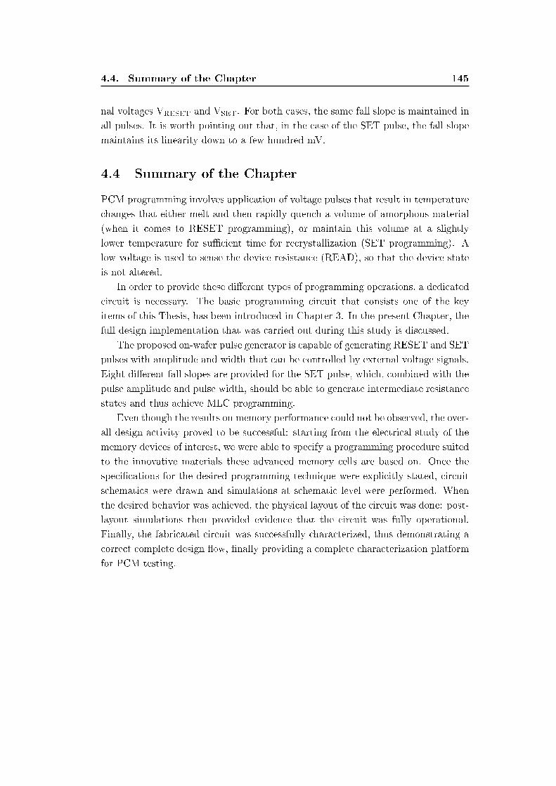
4.4. Summary of the Chapter 145
nal voltages VRESET and VSET. For both cases, the same fall slope is maintained in
all pulses. It is worth pointing out that, in the case of the SET pulse, the fall slope
maintains its linearity down to a few hundred mV.
4.4 Summary of the Chapter
PCM programming involves application of voltage pulses that result in temperature
changes that either melt and then rapidly quench a volume of amorphous material
(when it comes to RESET programming), or maintain this volume at a slightly
lower temperature for sucient time for recrystallization (SET programming). A
low voltage is used to sense the device resistance (READ), so that the device state
is not altered.
In order to provide these dierent types of programming operations, a dedicated
circuit is necessary. The basic programming circuit that consists one of the key
items of this Thesis, has been introduced in Chapter 3. In the present Chapter, the
full design implementation that was carried out during this study is discussed.
The proposed on-wafer pulse generator is capable of generating RESET and SET
pulses with amplitude and width that can be controlled by external voltage signals.
Eight dierent fall slopes are provided for the SET pulse, which, combined with the
pulse amplitude and pulse width, should be able to generate intermediate resistance
states and thus achieve MLC programming.
Even though the results on memory performance could not be observed, the over-
all design activity proved to be successful: starting from the electrical study of the
memory devices of interest, we were able to specify a programming procedure suited
to the innovative materials these advanced memory cells are based on. Once the
specications for the desired programming technique were explicitly stated, circuit
schematics were drawn and simulations at schematic level were performed. When
the desired behavior was achieved, the physical layout of the circuit was done: post-
layout simulations then provided evidence that the circuit was fully operational.
Finally, the fabricated circuit was successfully characterized, thus demonstrating a
correct complete design ow, nally providing a complete characterization platform
for PCM testing.

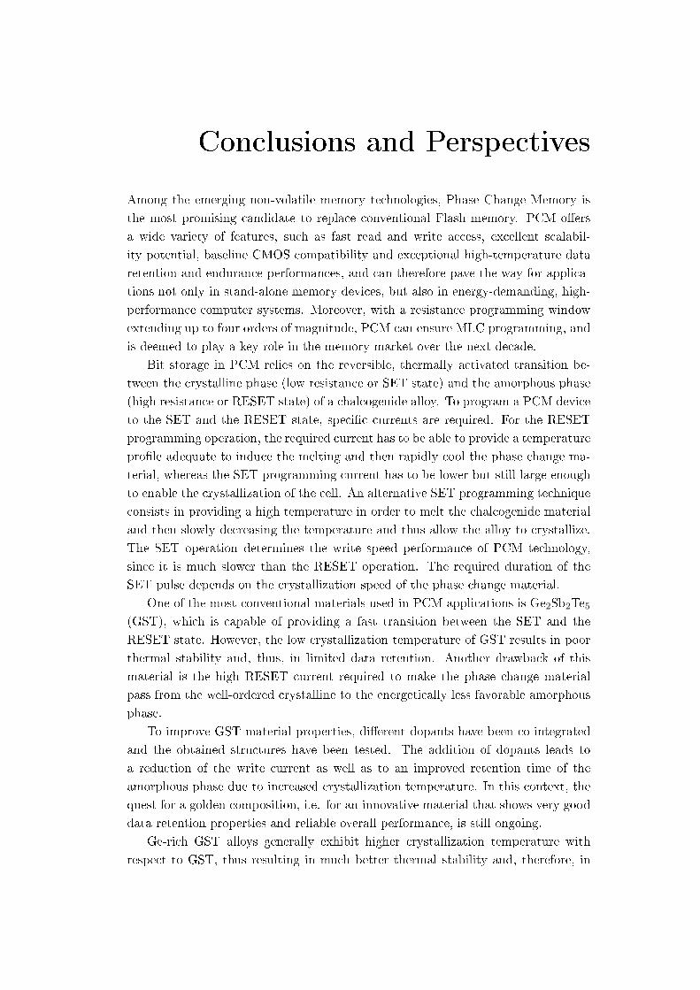
Conclusions and Perspectives
Among the emerging non-volatile memory technologies, Phase Change Memory is
the most promising candidate to replace conventional Flash memory. PCM oers
a wide variety of features, such as fast read and write access, excellent scalabil-
ity potential, baseline CMOS compatibility and exceptional high-temperature data
retention and endurance performances, and can therefore pave the way for applica-
tions not only in stand-alone memory devices, but also in energy-demanding, high-
performance computer systems. Moreover, with a resistance programming window
extending up to four orders of magnitude, PCM can ensure MLC programming, and
is deemed to play a key role in the memory market over the next decade.
Bit storage in PCM relies on the reversible, thermally activated transition be-
tween the crystalline phase (low resistance or SET state) and the amorphous phase
(high resistance or RESET state) of a chalcogenide alloy. To program a PCM device
to the SET and the RESET state, specic currents are required. For the RESET
programming operation, the required current has to be able to provide a temperature
prole adequate to induce the melting and then rapidly cool the phase change ma-
terial, whereas the SET programming current has to be lower but still large enough
to enable the crystallization of the cell. An alternative SET programming technique
consists in providing a high temperature in order to melt the chalcogenide material
and then slowly decreasing the temperature and thus allow the alloy to crystallize.
The SET operation determines the write speed performance of PCM technology,
since it is much slower than the RESET operation. The required duration of the
SET pulse depends on the crystallization speed of the phase change material.
One of the most conventional materials used in PCM applications is Ge2Sb2Te5(GST), which is capable of providing a fast transition between the SET and the
RESET state. However, the low crystallization temperature of GST results in poor
thermal stability and, thus, in limited data retention. Another drawback of this
material is the high RESET current required to make the phase change material
pass from the well-ordered crystalline to the energetically less favorable amorphous
phase.
To improve GST material properties, dierent dopants have been co-integrated
and the obtained structures have been tested. The addition of dopants leads to
a reduction of the write current as well as to an improved retention time of the
amorphous phase due to increased crystallization temperature. In this context, the
quest for a golden composition, i.e. for an innovative material that shows very good
data retention properties and reliable overall performance, is still ongoing.
Ge-rich GST alloys generally exhibit higher crystallization temperature with
respect to GST, thus resulting in much better thermal stability and, therefore, in
148 Conclusions and Perspectives
better data retention. The introduction of N into Ge enriched GST seems to further
enhance PCM performance.
Nonetheless, Ge-rich GST alloys demonstrate slow crystallization speed with
respect to GST and a non-negligible residual resistance drift phenomenon in the SET
state. The drift of the Low Resistance State of the Ge-rich GST can be reduced when
N is co-incorporated into the material. The recrystallization cartographies provided
for the study of the crystallization speed of the considered materials highlight the
need for a specic current versus time prole to achieve a SET state where the
LRS drift is reduced. To obtain the desired current versus time prole, innovative
programming techniques need to be implemented.
Among them, the R-SET pulse, which consists of a sequence of a RESET pulse
followed directly by a SET pulse with a linearly decreasing fall slope, is capable of
achieving a really low resistance SET state, with a drift coecient comparable to
the one obtained by means of time-consuming Staircase Down programming proce-
dures. The R-SET pulse sequence takes advantage of the threshold voltage decrease
occurring after the application of a RESET pulse to the cell, and brings the memory
cell to the SET state with a reduced programming voltage, thus protecting the cell
from possible excessive current overshoots during switching.
An additional programming technique that has been engineered in order to deal
with the SET state resistance distribution dispersion Ge-rich GST demonstrates,
consists in linearly decreasing the temperature in the active region of the memory
device. To this end, the fall slope of the applied voltage pulse has to be proportional
to the square root of time. The linear decrease rate of the temperature developed
in the memory device with this approach has been shown to lead to bigger crystal
grains in the active region of the phase change material and, thus, to a resistance
state of lower value, which exhibits a lower drift.
N-doped Ge-rich GST is an ideal candidate for MLC storage, thanks to the low
crystallization speed it demonstrates when compared to conventional GST. More
specically, the smooth transition between the SET and the RESET state allows
the occurrence of intermediate resistance states even when the pulse amplitude or
other pulse characteristics, such as time width and/or fall time, are aected by
moderate variability. Studying the recrystallization cartographies of this material,
the optimal characteristics of the programming current pulses required to bring
the memory cell to a target intermediate resistance level by using a single-pulse
procedure were determined.
For this purpose, a current pulse generator capable of providing current pro-
gramming pulses with the required characteristics has been presented. The circuit
is capable of providing multiple resistance levels which show modest variation when
the applied programming pulse varies due to fabrication process spreads. The ac-
curacy of the programmed resistance levels, which has been estimated by means of
Conclusions and Perspectives 149
Montecarlo simulations, highlights the eectiveness of the presented technique, thus
making the proposed circuit a viable solution for programming multiple resistance
levels per cell.
In order to program the cells with the proposed techniques, an on-wafer pulse
generator has been designed and implemented. The circuit provides the possibility
to program PCM cells to the RESET or the SET state, generating pulses whose
characteristics can be easily controlled. More specically, the amplitude and the
width of SET and RESET pulses can be controlled by means of external voltage
signals and, for SET programming, an additional selection between a pulse with a
linear voltage decrease and a pulse inducing a linearly decreasing temperature prole
(also selecting the fall slope of the pulse) is possible. Therefore, the presented pulse
generator allows full control of the pulse characteristics and can t the crystallization
demands of a variety of materials under study, enabling accurate programming of
phase change memory devices based on alternative-to-GST materials.
Even though the device performance of PCM seems to be optimized thanks to
N doping of Ge-rich GST, the research for a material that oers the best trade-
o between high temperature data retention and SET state performance is still
ongoing. The peculiar crystallization mechanism resulting in the resistance drift of
the SET state has been recently gured out and the phase change alloy featuring
an optimized stoichiometry represents a great candidate for Multilevel Cell storage.
Once the mechanisms causing the residual drift phenomenon in the intermediate
resistance states are fully understood, the reliability of PCM MLC storage will be
improved and the candidate material will be able to oer intermediate resistance
states whose content does not evolve over time.
A further interesting development of PCM technology will be the study of the
device behavior when the cell architecture is changed. The measurements performed
in the context of this Thesis were carried out on state-of-the-art Wall 1R devices.
Integrating innovative phase change materials in more advanced cell architectures,
such as the Conned architecture, is challenging, but the advantages coming from
that approach, such as the good thermal connement of the active volume and the
consequent increased power eciency, will be evident in the nal product. However,
as pointed out in Chapter 1, the resistance control of the conned element can be
achieved only by partially recrystallizing the phase change material (which is entirely
involved in the melting procedure) at the end of the programming procedure, which
requires a highly accurate control of the electrical pulse shape applied to the cell.
This necessitates highly reliable selector devices (diodes or transistors) allowing
accurate monitoring of the programming current.
As far as the design implementation of the pulse generator presented in this
Thesis is concerned, several things should be improved in order to enable more
accurate device programming. One of the main issues to be improved is the design of
150 Conclusions and Perspectives
the unity-gain buer that provides the necessary current driving capability, targeting
the improvement of the poor performance of the pull-down transistor in the output
stage. More specically, a more suitably designed operational amplier may be
implemented in order to provide high dc gain and reproduce the voltage pulses with
adequate accuracy.
Regarding the control of the fall slopes of the generated signals, the design
approach that was followed includes the on-chip generation of currents, with the
generated current amplitude being provided by generated control signals. The bias
current generator that was implemented is aected by large spreads due to the
fabrication process and large variations with operating conditions.
As a general approach, it is better to provide one current with an external source
or use an external resistor connected between the supply voltage and an internal
diode-connected transistor. The obtained current, which will then be mirrored with
dierent mirror factors, is obviously aected by spreads and variations with oper-
ating conditions but, changing the value of the resistor, the desired current can be
obtained with reasonable accuracy.
Nevertheless, one of the most important perspectives related to the present work
is the study of the fabricated circuit programming and the eects thereof on device
performance. More specically, while it has been possible to analyze the eects of
the R-SET pulse on PCM cells thanks to the electrical characterization equipment
that enabled us to generate this pulse sequence, the results of the application of the
pulses inducing a linear temperature prole in the cell are still to be experimentally
investigated.
Furthermore, given that eight dierent fall slopes of the SET pulse can be pro-
vided at the output of the designed circuit, the impact of programming on the
generated (intermediate) resistance states can also be of great interest, especially
when combined with a varying width of the generated pulses. Once the optimization
of circuit operation and device performance are ensured, the circuit may be further
developed in order to be used in an array of phase change memory cells, also aiming
at exploring challenging solutions, such as the cross-point memory array.
In conclusion, it is an undeniable fact that PCM has started to be considered
as a real competitor in the non-volatile memory market. Being compatible with
standard CMOS processes and demonstrating a remarkable set of performances,
PCM has attracted the interest of many industrial competitors and turns out to
be a reference for other memory technologies. We believe that in the near future,
also thanks to the work presented in the current Thesis, the unique capabilities
of PCM will be exploited in dierent electronics systems, ranging from ultra high
performance memory subsystems to large-scale computing platforms.
Author's Publications List
Conferences
[1] A. Kiouseloglou, G. Navarro, A. Cabrini, G. Torelli and L. Perniola, Current
pulse generator for multilevel cell programming of innovative PCM, Interna-
tional Conference on IC Design & Technology (ICICDT), 2015.
[2] A. Kiouseloglou, G. Navarro, A. Cabrini, L. Perniola and G. Torelli, Opti-
mized temperature prole based pulse generator for innovative Phase Change
Memory, IEEE 13th New Circuits and Systems Conference (NEWCAS), 2015.
[3] A. Kiouseloglou, E. Covi, G. Navarro, A. Cabrini, L. Perniola and G. Torelli,
A circuit for linearly decreasing temperature SET programming of PCM based
on Ge-rich GST, 11th Ph.D. Research in Microelectronics and Electronics
(PRIME), 2015.
[4] A. Kiouseloglou, E. Covi, G. Navarro, A. Cabrini, L. Perniola and G. Torelli,
Optimal programming with voltage-controlled temperature prole to reduce
SET state distribution dispersion in PCM, 21st IEEE International Conference
on Electronics, Circuits and Systems (ICECS), 2014.
[5] G. Navarro, M. Coué, A. Kiouseloglou, V. Sousa, P. Noé, F. Fillot, V. Delaye,
A. Persico, A. Roule, C. Sabbione, M. Bernard, D. Blachier, A. Cabrini, G.
Torelli, P. Zuliani, R. Annunziata, E. Palumbo, M. Borghi, G. Reimbold and
L. Perniola, SET performance improvement in phase-change memory based on
innovative materials featuring high temperature data retention, European Phase
Change and Ovonics Symposium (EPCOS), 2014.
[6] A. Kiouseloglou, G. Navarro, A. Cabrini, G. Torelli and L. Perniola, Op-
timization of Low-Resistance State performance in Ge-rich GST phase change
memory, 10th Ph.D. Research in Microelectronics and Electronics (PRIME),
2014.
[7] A. Kiouseloglou, E. Covi, G. Navarro, A. Cabrini, L. Perniola and G. Torelli,
Temperature study of high-drive capability buer for phase change memories,
10th Ph.D. Research in Microelectronics and Electronics (PRIME), 2014.
[8] E. Covi, A. Kiouseloglou, A. Cabrini and G. Torelli, Compact model for phase
change memory cells, 10th Ph.D. Research in Microelectronics and Electronics
(PRIME), 2014.
152 Author's Publications List
[9] G. Navarro, M. Coué, A. Kiouseloglou, P. Noé, F. Fillot, V. Delaye, A. Per-
sico, A. Roule, M. Bernard, C. Sabbione, D. Blachier, V. Sousa, L. Perniola,
S. Maitrejean, A. Cabrini, G. Torelli, P. Zuliani, R. Annunziata, E. Palumbo,
M. Borghi, G. Reimbold and B. De Salvo, Trade-o between SET and data re-
tention performance thanks to innovative materials for phase-change memory,
IEEE International Electron Devices Meeting (IEDM), 2013.
Journal articles
[10] A. Kiouseloglou, G. Navarro, V. Sousa, A. Persico, A. Roule, A. Cabrini, G.
Torelli, S. Maitrejean, G. Reimbold, B. De Salvo, F. Clermidy and L. Perniola,
A novel programming technique to boost low-resistance state performance in
Ge-Rich GST phase change memory, IEEE Transactions on Electron Devices,
vol. 61, no. 5, pp. 1246 - 1254, May 2014.
Bibliography
[1] M. Castells, End of Millennium, The Information Age: Economy, Society
and Culture, vol. III, Wiley-Blackwell, Malden, MA, 2000.
[2] R.D. Isaac, The future of CMOS technology, IBM J. Res. Develop., vol. 44,
no. 3, 2000.
[3] K. Kim and Gwanhyeob K., The prospect on semiconductor memory in nano
era, Solid-State and Integrated Circuits Technology, 2004. Proceedings. 7th
International Conference on, Oct 2004, vol. 1, pp. 662667 vol.1.
[4] J.E. Brewer, Lest we forget: NVSM from origins to the "beyond CMOS"
era, Non-Volatile Memory Technology Symposium, 2004, Nov 2004, pp. 1.
[5] G.W. Burr, B.N. Kurdi, J.C. Scott, C.H. Lam, K. Gopalakrishnan and R.S.
Shenoy, Overview of candidate device technologies for storage-class memory,
IBM Journal of Research and Development, vol. 52, no. 4.5, pp. 449464, July
2008.
[6] D.J. Wouters, R. Waser and M. Wuttig, Phase-Change and Redox-Based
Resistive Switching Memories, Proceedings of the IEEE, vol. 103, no. 8,
pp. 12741288, Aug 2015.
[7] C.H. Lam, The Quest for the Universal Semiconductor Memory, Electron
Devices and Solid-State Circuits, 2005 IEEE Conference on, Dec 2005, pp.
327331.
[8] S. Aritome, Advanced ash memory technology and trends for le storage
application, Electron Devices Meeting, 2000. IEDM '00. Technical Digest.
International, Dec 2000, pp. 763766.
[9] R. Bez, E. Camerlenghi, A. Modelli and A. Visconti, Introduction to ash
memory, Proceedings of the IEEE, vol. 91, no. 4, pp. 489502, April 2003.
[10] J. Meena, S. Sze, U. Chand and T.-Y. Tseng, Overview of emerging non-
volatile memory technologies, Nanoscale Research Letters, vol. 9, no. 1, 2014.
[11] MarketsandMarkets Analysis, Next Generation Memory Market by Tech-
nology (Nonvolatile memory (MRAM, FRAM, PCM, and RRAM), Volatile
Memory (DRAM (T-RAM, T-T-RAM, and others) and SRAM (Z-RAM and
others), Application and Geography - Global Forecast to 2013 - 2020, mar-
ketsandmarkets.com, Jan 2015.
154 Bibliography
[12] A. Fazio, Future directions of non-volatile memory in compute applications,
Electron Devices Meeting (IEDM), 2009 IEEE International, Dec 2009, pp.
14.
[13] Huang Jin and N. Manjikian, Embedded memory in system-on-chip design:
architecture and prototype implementation, Electrical and Computer En-
gineering, 2003. IEEE CCECE 2003. Canadian Conference on, May 2003,
vol. 1, pp. 141146 vol.1.
[14] P. Pavan, R. Bez, P. Olivo and E. Zanoni, Flash memory cells-an overview,
Proceedings of the IEEE, vol. 85, no. 8, pp. 12481271, Aug 1997.
[15] L. Crippa, R. Micheloni, I. Motta and M. Sangalli, Nonvolatile Memories:
NOR vs. NAND Architectures, Memories in Wireless Systems, R. Micheloni,
G. Campardo and P. Olivo, Eds., Signals and Communication Technology, pp.
2953. Springer Berlin Heidelberg, 2008.
[16] J.-G. Zhu, Magnetoresistive Random Access Memory: The Path to Compet-
itiveness and Scalability, Proceedings of the IEEE, vol. 96, no. 11, pp. 1786
1798, Nov 2008.
[17] T.P. Ma and J.-P. Han, Why is nonvolatile ferroelectric memory eld-eect
transistor still elusive?, Electron Device Letters, IEEE, vol. 23, no. 7, pp. 386
388, July 2002.
[18] C.F. Pulvari, Ferroelectrics and their Memory Applications, Component
Parts, IRE Transactions on, vol. 3, no. 1, pp. 311, Mar 1956.
[19] H. Akinaga and H. Shima, Resistive Random Access Memory (ReRAM)
Based on Metal Oxides, Proceedings of the IEEE, vol. 98, no. 12, pp. 2237
2251, Dec 2010.
[20] L.O. Chua, Memristor-The missing circuit element, Circuit Theory, IEEE
Transactions on, vol. 18, no. 5, pp. 507519, Sep 1971.
[21] D. Garbin, O. Bichler, E. Vianello, Q. Rafhay, C. Gamrat, L. Perniola,
G. Ghibaudo and B. DeSalvo, Variability-tolerant Convolutional Neural
Network for Pattern Recognition applications based on OxRAM synapses,
Electron Devices Meeting (IEDM), 2014 IEEE International, Dec 2014, pp.
28.4.128.4.4.
[22] Shimeng Y., X. Guan and H.-S.P. Wong, On the stochastic nature of resistive
switching in metal oxide RRAM: Physical modeling, monte carlo simulation,
and experimental characterization, Electron Devices Meeting (IEDM), 2011
IEEE International, Dec 2011, pp. 17.3.117.3.4.
Bibliography 155
[23] M.N. Kozicki, C. Gopalan, M. Balakrishnan, P. Mira and M. Mitkova, Non-
volatile memory based on solid electrolytes, Non-Volatile Memory Technology
Symposium, 2004, Nov 2004, pp. 1017.
[24] M. Kund, G. Beitel, C.-U. Pinnow, T. Rohr, J. Schumann, R. Symanczyk,
K.-D. Ufert and G. Muller, Conductive bridging RAM (CBRAM): an emerg-
ing non-volatile memory technology scalable to sub 20nm, Electron Devices
Meeting, 2005. IEDM Technical Digest. IEEE International, Dec 2005, pp.
754757.
[25] J. Guy, G. Molas, E. Vianello, F. Longnos, S. Blanc, C. Carabasse,
M. Bernard, J.F. Nodin, A. Tooli, J. Cluzel, P. Blaise, P. Dorion, O. Cueto,
H. Grampeix, E. Souchier, T. Cabout, P. Brianceau, V. Balan, A. Roule,
S. Maitrejean, L. Perniola and B. De Salvo, Investigation of the phys-
ical mechanisms governing data-retention in down to 10nm nano-trench
Al2O3/CuTeGe conductive bridge RAM (CBRAM), Electron Devices Meet-
ing (IEDM), 2013 IEEE International, Dec 2013, pp. 30.2.130.2.4.
[26] M. Barci, J. Guy, G. Molas, E. Vianello, A. Tooli, J. Cluzel, A. Roule,
M. Bernard, C. Sabbione, L. Perniola and B. De Salvo, Impact of SET and
RESET conditions on CBRAM high temperature data retention, Reliability
Physics Symposium, 2014 IEEE International, June 2014, pp. 5E.3.15E.3.4.
[27] A.T. Waterman, XXI. On the positive ionization from certain hot salts,
together with some observations on the electrical properties of molybdenite
at high temperatures, Philosophical Magazine Series 6, vol. 33, no. 195,
pp. 225247, 1917.
[28] A. T. Waterman, The Electrical Conductivity of Molybdenite, Phys. Rev.,
vol. 21, pp. 540549, May 1923.
[29] S. R. Ovshinsky, Reversible Electrical Switching Phenomena in Disordered
Structures, Phys. Rev. Lett., vol. 21, pp. 14501453, Nov 1968.
[30] H. Iizuka, T. Sato, F. Masuoka, K. Ohuchi, H. Hara and Y. Takeishi, "A
fully-decoded 2048-bit avalanche-injection type, electrically alterable ROM",
Electron Devices Meeting, 1972 International, 1972, vol. 18, pp. 45.
[31] S. Lai and T. Lowrey, OUM - A 180 nm nonvolatile memory cell element tech-
nology for stand alone and embedded applications, Electron Devices Meeting,
2001. IEDM '01. Technical Digest. International, Dec 2001, pp. 36.5.136.5.4.
[32] I. Friedrich, V. Weidenhof, W. Njoroge, P. Franz and M. Wuttig, Structural
transformations of Ge2Sb2Te5 lms studied by electrical resistance measure-
ments, Journal of Applied Physics, vol. 87, no. 9, pp. 41304134, 2000.
156 Bibliography
[33] G. Navarro, N. Pashkov, M. Suri, V. Sousa, L. Perniola, S. Maitrejean, A. Per-
sico, A. Roule, A. Tooli, B. De Salvo, P. Zuliani and R. Annunziata, Elec-
trical Performances of Tellurium-Rich GexTe1-x Phase Change Memories,
Memory Workshop (IMW), 2011 3rd IEEE International, May 2011, pp. 14.
[34] J. A. Kalb, F. Spaepen and M. Wuttig, Kinetics of crystal nucleation in un-
dercooled droplets of Sb- and Te-based alloys used for phase change recording,
Journal of Applied Physics, vol. 98, no. 5, pp. , 2005.
[35] M. Krbal, A. V. Kolobov, P. Fons, J. Tominaga, S. R. Elliott, J. Hegedus,
A. Giussani, K. Perumal, R. Calarco, T. Matsunaga, N. Yamada, K. Nitta and
T. Uruga, Crystalline GeTe-based phase-change alloys: Disorder in order,
Phys. Rev. B, vol. 86, pp. 045212, Jul 2012.
[36] P. Nath and K. L. Chopra, Thermal conductivity of amorphous and crys-
talline Ge and GeTe lms, Phys. Rev. B, vol. 10, pp. 34123418, Oct 1974.
[37] J. Zhang, R. Huang, L. Shi, L. Wang, F. Wei, T. Kong and G. Cheng, Bi
doping modulating structure and phase-change properties of GeTe nanowires,
Applied Physics Letters, vol. 102, no. 6, pp. , 2013.
[38] W. Gawelda, J. Siegel, C. N. Afonso, V. Plausinaitiene, A. Abrutis and
C. Wiemer, Dynamics of laser-induced phase switching in GeTe lms, Jour-
nal of Applied Physics, vol. 109, no. 12, pp. , 2011.
[39] K. L. Chopra and S. K. Bahl, Amorphous versus Crystalline GeTe Films. I.
Growth and Structural Behavior, Journal of Applied Physics, vol. 40, no. 10,
pp. 41714178, 1969.
[40] F. Pellizzer, A. Pirovano, F. Ottogalli, M. Magistretti, M. Scaravaggi, P. Zu-
liani, M. Tosi, A. Benvenuti, P. Besana, S. Cadeo, T. Marangon, R. Morandi,
R. Piva, A. Spandre, R. Zonca, A. Modelli, E. Varesi, T. Lowrey, A. Lacaita,
G. Casagrande, P. Cappelletti and R. Bez, Novel microtrench phase-change
memory cell for embedded and stand-alone non-volatile memory applications,
VLSI Technology, 2004. Digest of Technical Papers. 2004 Symposium on, June
2004, pp. 1819.
[41] D. Ielmini, A.L. Lacaita, A. Pirovano, F. Pellizzer and R. Bez, Analysis of
phase distribution in phase-change nonvolatile memories, Electron Device
Letters, IEEE, vol. 25, no. 7, pp. 507509, July 2004.
[42] A. Pirovano, A.L. Lacaita, A. Benvenuti, F. Pellizzer and R. Bez, Electronic
switching in phase-change memories, Electron Devices, IEEE Transactions
on, vol. 51, no. 3, pp. 452459, March 2004.
Bibliography 157
[43] H.-S.P. Wong, S. Raoux, SangBum K., Jiale L., J. P. Reifenberg, B. Rajen-
dran, M. Asheghi and K. E. Goodson, Phase Change Memory, Proceedings
of the IEEE, vol. 98, no. 12, pp. 22012227, Dec 2010.
[44] D. Ielmini, D. Mantegazza, A.L. Lacaita, A. Pirovano and F. Pellizzer,
Switching and programming dynamics in phase-change memory cells, Solid-
State Electronics, vol. 49, no. 11, pp. 1826 1832, 2005, Special Issue:Papers
selected from the 1st International Conference on Memory Technology and
Design - ICMTD'05.
[45] A. Redaelli, A. Pirovano, F. Pellizzer, A.L. Lacaita, D. Ielmini and R. Bez,
Electronic switching eect and phase-change transition in chalcogenide ma-
terials, Electron Device Letters, IEEE, vol. 25, no. 10, pp. 684686, Oct
2004.
[46] D. Ielmini, Threshold switching mechanism by high-eld energy gain in the
hopping transport of chalcogenide glasses, Phys. Rev. B, vol. 78, pp. 035308,
Jul 2008.
[47] A. V. Kolobov, P. Fons, J. Tominaga, A.I. Frenkel, A. L. Ankudinov and
T. Uruga, Local structure of Ge-Sb-Te and its modication upon the phase
transition, Journal of Ovonic Research, vol. 1, no. 1, pp. 2124, Feb 2005.
[48] Motoyasu Terao, Takahiro Morikawa and Takeo Ohta, Electrical Phase-
Change Memory: Fundamentals and State of the Art, Japanese Journal
of Applied Physics, vol. 48, no. 8R, pp. 080001, 2009.
[49] Melvin Avrami, Kinetics of Phase Change. I General Theory, The Journal
of Chemical Physics, vol. 7, no. 12, pp. 11031112, 1939.
[50] Melvin Avrami, Kinetics of Phase Change. II Transformation Time Relations
for Random Distribution of Nuclei, The Journal of Chemical Physics, vol. 8,
no. 2, pp. 212224, 1940.
[51] Melvin Avrami, Granulation, Phase Change, and Microstructure Kinetics of
Phase Change. III, The Journal of Chemical Physics, vol. 9, no. 2, pp. 177
184, 1941.
[52] Guo-Fu Zhou, Materials aspects in phase change optical recording, Materials
Science and Engineering: A, vol. 304-306, pp. 73 80, 2001, RQ10, Tenth
International Conference on Rapidly Quenched and Metastable Materials.
[53] V. M. Fokin, N. S. Yuritsyn and E. D. Zanotto, Nucleation and Crystallization
Kinetics in Silicate Glasses: Theory and Experiment, pp. 74125, Wiley-VCH
Verlag GmbH and Co. KGaA, 2005.
158 Bibliography
[54] P. Pauer, S. R. Elliott. Physics of amorphous materials. Longman Group
Ltd., London, New York, 1984., Crystal Research and Technology, vol. 20,
no. 9, pp. 12381238, 1985.
[55] J. Hegedus and S. R. Elliott, Microscopic origin of the fast crystallization
ability of Ge-Sb-Te phase-change memory materials, Nat Mater, vol. 7, no. 5,
pp. 399405, May 2008.
[56] A. V. Kolobov, P. Fons, A. I. Frenkel, A. L. Ankudinov, J. Tominaga and
T. Uruga, Understanding the phase-change mechanism of rewritable optical
media, Nat Mater, vol. 3, no. 10, pp. 703708, 2004.
[57] M. Boniardi, D. Ielmini, S. Lavizzari, A.L. Lacaita, A. Redaelli and
A. Pirovano, Statistics of Resistance Drift Due to Structural Relaxation
in Phase-Change Memory Arrays, Electron Devices, IEEE Transactions on,
vol. 57, no. 10, pp. 26902696, Oct 2010.
[58] A. Redaelli, A. Pirovano, A. Locatelli and F. Pellizzer, Numerical Imple-
mentation of Low Field Resistance Drift for Phase Change Memory Simula-
tions, Non-Volatile Semiconductor Memory Workshop, 2008 and 2008 Inter-
national Conference on Memory Technology and Design. NVSMW/ICMTD
2008. Joint, May 2008, pp. 3942.
[59] M. Wuttig, D. Lusebrink, D. Wamwangi, W. Welnic, M. Gilleszen and
R. Dronskowski, Nat Mater, Electron Devices, IEEE Transactions on, vol. 6,
no. 2, pp. 122128, Feb 2007.
[60] J. Luckas, A. Piarristeguy, G. Bruns, P. Jost, S. Grothe, R. M. Schmidt,
C. Longeaud and M. Wuttig, Stoichiometry dependence of resistance drift
phenomena in amorphous GeSnTe phase-change alloys, Journal of Applied
Physics, vol. 113, no. 2, pp. , 2013.
[61] SangBum Kim, Byoungil Lee, M. Asheghi, F. Hurkx, J. P. Reifenberg, K. E.
Goodson and H.-S.P. Wong, Resistance and Threshold Switching Voltage
Drift Behavior in Phase-Change Memory and Their Temperature Dependence
at Microsecond Time Scales Studied Using a Micro-Thermal Stage, Electron
Devices, IEEE Transactions on, vol. 58, no. 3, pp. 584592, March 2011.
[62] M. Boniardi, A. Redaelli, A. Pirovano, I. Tortorelli, D. Ielmini and F. Pel-
lizzer, A physics-based model of electrical conduction decrease with time in
amorphous Ge2Sb2Te5, Journal of Applied Physics, vol. 105, no. 8, pp. ,
2009.
Bibliography 159
[63] D. Ielmini, A.L. Lacaita and D. Mantegazza, Recovery and Drift Dynamics
of Resistance and Threshold Voltages in Phase-Change Memories, Electron
Devices, IEEE Transactions on, vol. 54, no. 2, pp. 308315, Feb 2007.
[64] P. Junsangsri, Jie Han and F. Lombardi, A system-level scheme for resistance
drift tolerance of a multilevel phase change memory, Defect and Fault Toler-
ance in VLSI and Nanotechnology Systems (DFT), 2014 IEEE International
Symposium on, Oct 2014, pp. 6368.
[65] C. Liu and C. Yang, Improving multilevel PCM reliability through age-aware
reading and writing strategies, Computer Design (ICCD), 2014 32nd IEEE
International Conference on, Oct 2014, pp. 264269.
[66] N. Papandreou, H. Pozidis, T. Mittelholzer, G.F. Close, M. Breitwisch, C. Lam
and E. Eleftheriou, Drift-Tolerant Multilevel Phase-Change Memory, Mem-
ory Workshop (IMW), 2011 3rd IEEE International, May 2011, pp. 14.
[67] J. L. M. Oosthoek, K. Attenborough, G. A. M. Hurkx, F. J. Jedema, D. J.
Gravesteijn and B. J. Kooi, Evolution of cell resistance, threshold voltage and
crystallization temperature during cycling of line-cell phase-change random
access memory, Journal of Applied Physics, vol. 110, no. 2, pp. , 2011.
[68] M. Boniardi and D. Ielmini, Physical origin of the resistance drift exponent in
amorphous phase change materials, Applied Physics Letters, vol. 98, no. 24,
pp. , 2011.
[69] N. Ciocchini, M. Cassinerio, D. Fugazza and D. Ielmini, Modeling of
Threshold-Voltage Drift in Phase-Change Memory (PCM) Devices, Electron
Devices, IEEE Transactions on, vol. 59, no. 11, pp. 30843090, Nov 2012.
[70] J. Li, B. Luan and C. Lam, Resistance drift in phase change memory,
Reliability Physics Symposium (IRPS), 2012 IEEE International, April 2012,
pp. 6C.1.16C.1.6.
[71] M.J. Kang, T.J. Park, Y.W. Kwon, D.H. Ahn, Y.S. Kang, H. Jeong, S.J. Ahn,
Y.J. Song, B.C. Kim, S.W. Nam, H.K. Kang, G.T. Jeong and C.H. Chung,
PRAM cell technology and characterization in 20nm node size, Electron
Devices Meeting (IEDM), 2011 IEEE International, Dec 2011, pp. 3.1.13.1.4.
[72] R. Bez, P. Cappelletti, G. Servalli and A. Pirovano, Phase Change Memories
have taken the eld, Memory Workshop (IMW), 2013 5th IEEE International,
May 2013, pp. 1316.
160 Bibliography
[73] A. Pirovano, A.L. Lacaita, A. Benvenuti, F. Pellizzer, S. Hudgens and R. Bez,
Scaling analysis of phase-change memory technology, Electron Devices Meet-
ing, 2003. IEDM '03 Technical Digest. IEEE International, Dec 2003, pp.
29.6.129.6.4.
[74] A. Pirovano, F. Pellizzer, I. Tortorelli, R. Harrigan, M. Magistretti,
P. Petruzza, E. Varesi, D. Erbetta, T. Marangon, F. Bedeschi, R. Fackenthal,
G. Atwood and R. Bez, Self-aligned microtrench phase-change memory cell
architecture for 90nm technology and beyond, Solid State Device Research
Conference, 2007. ESSDERC 2007. 37th European, Sept 2007, pp. 222225.
[75] G. Servalli, A 45nm generation Phase Change Memory technology, Electron
Devices Meeting (IEDM), 2009 IEEE International, Dec 2009, pp. 14.
[76] M. Boniardi, A. Redaelli, C. Cupeta, F. Pellizzer, L. Crespi, G. D'Arrigo, A.L.
Lacaita and G. Servalli, Optimization metrics for Phase Change Memory
(PCM) cell architectures, Electron Devices Meeting (IEDM), 2014 IEEE
International, Dec 2014, pp. 29.1.129.1.4.
[77] C. Bergonzoni, M. Borghi and E. Palumbo, Reset Current Scaling in Phase-
Change Memory Cells: Modeling and Experiments, Electron Devices, IEEE
Transactions on, vol. 59, no. 2, pp. 283291, Feb 2012.
[78] J.I. Lee, H. Park, S.L. Cho, Y.L. Park, B.J. Bae, J.H. Park, J.S. Park, H.G.
An, J.S. Bae, D.H. Ahn, Y.T. Kim, H. Horii, S.A. Song, J.C. Shin, S.O.
Park, H.S. Kim, U-in Chung, J.T. Moon and B.-I. Ryu, Highly Scalable
Phase Change Memory with CVD GeSbTe for Sub 50nm Generation, VLSI
Technology, 2007 IEEE Symposium on, June 2007, pp. 102103.
[79] S.C. Lai, S. Kim, M. BrightSky, Y. Zhu, E. Joseph, R. Bruce, H.Y. Cheng,
A. Ray, S. Raoux, J.Y. Wu, T.Y. Wang, N.S. Cortes, C.M. Lin, Y.Y. Lin,
R. Cheek, E.K. Lai, M.H. Lee, H.L. Lung and C. Lam, A scalable volume-
conned phase change memory using physical vapor deposition, VLSI Tech-
nology (VLSIT), 2013 Symposium on, June 2013, pp. T132T133.
[80] Atwood R., The evolution of phase-change memory, EETimes, web journal,
2010.
[81] Yole Developpement, Resistive Memory Patent Landscape, 2014.
[82] Y. Fukuzumi, Y. Matsuoka, M. Kito, M. Kido, M. Sato, H. Tanaka, Y. Nagata,
Y. Iwata, H. Aochi and A. Nitayama, Optimal Integration and Characteris-
tics of Vertical Array Devices for Ultra-High Density, Bit-Cost Scalable Flash
Memory, Electron Devices Meeting, 2007. IEDM 2007. IEEE International,
Dec 2007, pp. 449452.

Bibliography 161
[83] T. Nirschl, J.B. Philipp, T.D. Happ, G.W. Burr, B. Rajendran, M.H. Lee,
A. Schrott, M. Yang, M. Breitwisch, C.F. Chen, E. Joseph, M. Lamorey,
R. Cheek, S.-H. Chen, S. Zaidi, S. Raoux, Y.C. Chen, Y. Zhu, R. Bergmann,
H.L. Lung and C. Lam, Write Strategies for 2 and 4-bit Multi-Level Phase-
Change Memory, Electron Devices Meeting, 2007. IEDM 2007. IEEE Inter-
national, Dec 2007, pp. 461464.
[84] R.F. Freitas and W.W. Wilcke, Storage-class memory: The next storage sys-
tem technology, IBM Journal of Research and Development, vol. 52, no. 4.5,
pp. 439447, July 2008.
[85] C.H. Lam, Storage Class Memory, Solid-State and Integrated Circuit Tech-
nology (ICSICT), 2010 10th IEEE International Conference on, Nov 2010, pp.
10801083.
[86] D. Kuzum, R. G. D. Jeyasingh, B. Lee and H.-S. P. Wong, Nanoelectronic
Programmable Synapses Based on Phase Change Materials for Brain-Inspired
Computing, Nano Letters, vol. 12, no. 5, pp. 21792186, 2012, PMID:
21668029.
[87] F. Clermidy, R. Heliot, A. Valentian, C. Gamrat, O. Bichler, M. Duranton,
B. Blehadj and O. Temam, Advanced technologies for brain-inspired comput-
ing, Design Automation Conference (ASP-DAC), 2014 19th Asia and South
Pacic, Jan 2014, pp. 563569.
[88] O.r Bichler, M. Suri, D. Querlioz, D. Vuillaume, B. DeSalvo and C. Gamrat,
Visual Pattern Extraction Using Energy-Ecient "2-PCM Synapse" Neuro-
morphic Architecture, Electron Devices, IEEE Transactions on, vol. 59, no. 8,
pp. 22062214, Aug 2012.
[89] D. Garbin, M. Suri, O. Bichler, D. Querlioz, C. Gamrat and B. DeSalvo, Prob-
abilistic neuromorphic system using binary phase-change memory (PCM)
synapses: Detailed power consumption analysis, Nanotechnology (IEEE-
NANO), 2013 13th IEEE Conference on, Aug 2013, pp. 9194.
[90] N. Papandreou, A. Pantazi, A. Sebastian, M. Breitwisch, C. Lam, H. Pozidis
and E. Eleftheriou, Multilevel phase-change memory, Electronics, Cir-
cuits, and Systems (ICECS), 2010 17th IEEE International Conference on,
Dec 2010, pp. 10171020.
[91] D-H. Kang, J.-H. Lee, J.H. Kong, D. Ha, J. Yu, C.Y. Um, J.H. Park, F. Yeung,
J.H. Kim, W.I. Park, Y.J. Jeon, M.K. Lee, J.H. Park, Y.J. Song, J.H. Oh, H.S.
Jeong and H.S. Jeong, Two-bit cell operation in diode-switch phase change
162 Bibliography
memory cells with 90nm technology, VLSI Technology, 2008 Symposium on,
June 2008, pp. 9899.
[92] N. Papandreou, A. Sebastian, A. Pantazi, M. Breitwisch, C. Lam, H. Pozidis
and E. Eleftheriou, Drift-resilient cell-state metric for multilevel phase-change
memory, Electron Devices Meeting (IEDM), 2011 IEEE International, Dec
2011, pp. 3.5.13.5.4.
[93] U. Russo, D. Ielmini, A. Redaelli and A.L. Lacaita, Modeling of Programming
and Read Performance in Phase-Change Memories Part I: Cell Optimization
and Scaling, Electron Devices, IEEE Transactions on, vol. 55, no. 2, pp. 506
514, Feb 2008.
[94] Jeung-hyun Jeong, Hyung-Woo Ahn, Suyoun Lee, Won Mok Kim, Jae-Geun
Ha and Byung-ki Cheong, Analysis and improvement of interfacial adhesion
of growth-dominant Ge-doped SbTe phase change materials, Applied Physics
Letters, vol. 94, no. 1, pp. , 2009.
[95] K.N. Chen, L. Krusin-Elbaum, C. Cabral, C. Lavoie, J. Sun and S. Rossnagel,
Thermal stress evaluation of a PCRAM material Ge2Sb2Te5, Non-Volatile
Semiconductor Memory Workshop, 2006. IEEE NVSMW 2006. 21st, Feb 2006,
pp. 9798.
[96] Kinam Kim and Su Jin Ahn, Reliability investigations for manufacturable
high density PRAM, Reliability Physics Symposium, 2005. Proceedings. 43rd
Annual. 2005 IEEE International, April 2005, pp. 157162.
[97] B. Gleixner, A. Pirovano, J. Sarkar, F. Ottogalli, E. Tortorelli, M. Tosi and
R. Bez, Data Retention Characterization of Phase-Change Memory Arrays,
Reliability physics symposium, 2007. proceedings. 45th annual. ieee interna-
tional, April 2007, pp. 542546.
[98] R. Bez, E. Camerlenghi, A. Modelli and A. Visconti, Introduction to ash
memory, Proceedings of the IEEE, vol. 91, no. 4, pp. 489502, April 2003.
[99] Joy Sarkar and Bob Gleixner, Evolution of phase change memory characteris-
tics with operating cycles: Electrical characterization and physical modeling,
Applied Physics Letters, vol. 91, no. 23, pp. , 2007.
[100] Sung-Hoon Hong and Heon Lee, Failure Analysis of Ge 2 Sb 2 Te 5 Based
Phase Change Memory, Japanese Journal of Applied Physics, vol. 47, no. 5R,
pp. 3372, 2008.
[101] A. Padilla, G. W. Burr, C. T. Rettner, T. Topuria, P. M. Rice, B. Jack-
son, K. Virwani, A. J. Kellock, D. Dupouy, A. Debunne, R. M. Shelby,
Bibliography 163
K. Gopalakrishnan, R. S. Shenoy and B. N. Kurdi, Voltage polarity eects in
Ge2Sb2Te5-based phase change memory devices, Journal of Applied Physics,
vol. 110, no. 5, pp. , 2011.
[102] I. Karpov, S. Savransky and V. Karpov, Mechanism of Threshold Switching
in Chalcogenide Phase Change Memory Devices, Non-Volatile Semiconductor
Memory Workshop, 2007 22nd IEEE, Aug 2007, pp. 5657.
[103] Suyoun Lee, Doo Seok Jeong, Jeung-hyun Jeong, Wu Zhe, Young-Wook Park,
Hyung-Woo Ahn and Byung-ki Cheong, A study on the temperature de-
pendence of the threshold switching characteristics of Ge2Sb2Te5, Applied
Physics Letters, vol. 96, no. 2, pp. , 2010.
[104] A. Redaelli, D. Ielmini, A.L. Lacaita, F. Pellizzer, A. Pirovano and R. Bez,
Impact of crystallization statistics on data retention for phase change mem-
ories, Electron Devices Meeting, 2005. IEDM Technical Digest. IEEE Inter-
national, Dec 2005, pp. 742745.
[105] U. Russo, D. Ielmini and A.L. Lacaita, Analytical Modeling of Chalcogenide
Crystallization for PCM Data-Retention Extrapolation, Electron Devices,
IEEE Transactions on, vol. 54, no. 10, pp. 27692777, Oct 2007.
[106] B. Gleixner, F. Pellizzer and R. Bez, Reliability characterization of Phase
Change Memory, Non-Volatile Memory Technology Symposium (NVMTS),
2009 10th Annual, Oct 2009, pp. 711.
[107] Q. Hubert, C. Jahan, A. Tooli, G. Navarro, S. Chandrashekar, P. Noe,
D. Blachier, V. Sousa, L. Perniola, J.-F. Nodin, A. Persico, R. Kies,
S. Maitrejean, A. Roule, E. Hena, M. Tessaire, P. Zuliani, R. Annunziata,
G. Pananakakis, G. Reimbold and B. De Salvo, Lowering the Reset Cur-
rent and Power Consumption of Phase-Change Memories with Carbon-Doped
Ge2Sb2Te5, Memory Workshop (IMW), 2012 4th IEEE International, May
2012, pp. 14.
[108] G. W. Burr, M. J. Breitwisch, M. Franceschini, D. Garetto, K. Gopalakrish-
nan, B. Jackson, B. Kurdi, C. Lam, L. A. Lastras, A. Padilla et al., Phase
change memory technology, Journal of Vacuum Science & Technology B,
vol. 28, no. 2, pp. 223262, 2010.
[109] H. Horii, J.H. Yi, J.H. Park, Y.H. Ha, I.G. Baek, S.O. Park, Y.N. Hwang, S.H.
Lee, Y.T. Kim, K.H. Lee, U-In Chung and J.T. Moon, A novel cell technology
using N-doped GeSbTe lms for phase change RAM, VLSI Technology, 2003.
Digest of Technical Papers. 2003 Symposium on, June 2003, pp. 177178.
164 Bibliography
[110] Robert M. Shelby and Simone Raoux, Crystallization dynamics of nitrogen-
doped Ge2Sb2Te5, Journal of Applied Physics, vol. 105, no. 10, pp. , 2009.
[111] Lina Wei-Wei Fang, Rong Zhao, Minghua Li, Kian-Guan Lim, Luping Shi,
Tow-Chong Chong and Yee-Chia Yeo, Dependence of the properties of
phase change random access memory on nitrogen doping concentration in
Ge2Sb2Te5, Journal of Applied Physics, vol. 107, no. 10, pp. , 2010.
[112] S. Privitera, E. Rimini and R. Zonca, Amorphous-to-crystal transition of
nitrogen- and oxygen-doped Ge2Sb2Te5 lms studied by in situ resistance
measurements, Applied Physics Letters, vol. 85, no. 15, pp. 30443046, 2004.
[113] G. Navarro, A. Persico, E. Hena, F. Aussenac, P. Noe, C. Jahan, L. Perniola,
V. Sousa, E. Vianello and B. De Salvo, Electrical performances of SiO2-doped
GeTe for phase-change memory applications, Reliability Physics Symposium
(IRPS), 2013 IEEE International, April 2013, pp. MY.9.1MY.9.5.
[114] Eunae Cho, Yong Youn and Seungwu Han, Enhanced amorphous stability of
carbon-doped Ge2Sb2Te5: Ab Initio investigation, Applied Physics Letters,
vol. 99, no. 18, pp. , 2011.
[115] Xilin Zhou, Liangcai Wu, Zhitang Song, Feng Rao, Min Zhu, Cheng Peng,
Dongning Yao, Sannian Song, Bo Liu and Songlin Feng, Carbon-doped
Ge2Sb2Te5 phase change material: A candidate for high-density phase change
memory application, Applied Physics Letters, vol. 101, no. 14, pp. , 2012.
[116] Q. Hubert, C. Jahan, A. Tooli, G. Navarro, S. Chandrashekar, P. Noe,
V. Sousa, L. Perniola, J.-F. Nodin, A. Persico, S. Maitrejean, A. Roule,
E. Hena, M. Tessaire, P. Zuliani, R. Annunziata, G. Reimbold,
G. Pananakakis and B. De Salvo, Carbon-doped Ge2Sb2Te5 phase-change
memory devices featuring reduced RESET current and power consumption,
Solid-State Device Research Conference (ESSDERC), 2012 Proceedings of the
European, Sept 2012, pp. 286289.
[117] H.L. Lung, M. Breitwisch, J.Y. Wu, Pei-Ying Du, Y. Zhu, M.H. Lee, Y.H.
Shih, E.K. Lai, R. Dasaka, T.Y. Wang, C.F. Chen, R. Cheek, A. Schrott,
E. Joseph, H.Y. Cheng, S. Raoux and C. Lam, A method to maintain
phase-change memory pre-coding data retention after high temperature sol-
der bonding process in embedded systems, VLSI Technology (VLSIT), 2011
Symposium on, June 2011, pp. 9899.
[118] L. Perniola, P. Noe, Q. Hubert, S. Souiki, G. Ghezzi, G. Navarro, A. Cabrini,
A. Persico, V. Delaye, D. Blachier, J.-P. Barnes, E. Hena, M. Tessaire,
Bibliography 165
E. Souchier, A. Roule, F. Fillot, J. Ferrand, A. Fargeix, F. Hippert, J.-Y.
Raty, C. Jahan, V. Sousa, G. Torelli, S. Maitrejean, B. De Salvo and G. Re-
imbold, Ti impact in C-doped phase-change memories compliant to Pb-free
soldering reow, Electron Devices Meeting (IEDM), 2012 IEEE International,
Dec 2012, pp. 18.7.118.7.4.
[119] H.Y. Cheng, T.H. Hsu, S. Raoux, J.Y. Wu, P.Y. Du, M. Breitwisch, Y. Zhu,
E.K. Lai, E. Joseph, S. Mittal, R. Cheek, A. Schrott, S.C. Lai, H.L. Lung and
C. Lam, A high performance phase change memory with fast switching speed
and high temperature retention by engineering the GexSbyTez phase change
material, Electron Devices Meeting (IEDM), 2011 IEEE International, Dec
2011, pp. 3.4.13.4.4.
[120] P. Zuliani, E. Varesi, E. Palumbo, M. Borghi, I. Tortorelli, D. Erbetta,
G. Dalla Libera, N. Pessina, A. Gandolfo, C. Prelini, L. Ravazzi and R. An-
nunziata, Overcoming Temperature Limitations in Phase Change Memo-
ries With Optimized GexSbyTez, Electron Devices, IEEE Transactions on,
vol. 60, no. 12, pp. 40204026, Dec 2013.
[121] Jing Li, Binquan Luan, T.H. Hsu, Y. Zhu, G. Martyna, D. Newns, H.Y. Cheng,
S. Raoux, H.L. Lung and C. Lam, Explore physical origins of resistance drift
in phase change memory and its implication for drift-insensitive materials,
Electron Devices Meeting (IEDM), 2011 IEEE International, Dec 2011, pp.
12.5.112.5.4.
[122] S. Kostylev and T. Lowrey, Drift of programmed resistance in electrical phase
change memory devices, European Phase Change and Ovonics Symposium,
Sep 2008, pp. 18.
[123] F. Bedeschi, C. Bono, E. Bonizzoni, C. Resta and G. Torelli, Staircase down
SET programming approach for phase change memories, Microelectronics
Journal, vol. 38, no. 10, pp. 1064 1069, 2007.
[124] G. Navarro, M. Coue, A. Kiouseloglou, P. Noe, F. Fillot, V. Delaye, A. Per-
sico, A. Roule, M. Bernard, C. Sabbione, D. Blachier, V. Sousa, L. Perniola,
S. Maitrejean, A. Cabrini, G. Torelli, P. Zuliani, R. Annunziata, E. Palumbo,
M. Borghi, G. Reimbold and B. De Salvo, Trade-o between SET and data
retention performance thanks to innovative materials for phase-change mem-
ory, Electron Devices Meeting (IEDM), 2013 IEEE International, Dec 2013,
pp. 21.5.121.5.4.
[125] D. Ielmini, S. Lavizzari, D. Sharma and A.L. Lacaita, Physical interpretation,
modeling and impact on phase change memory (PCM) reliability of resistance
166 Bibliography
drift due to chalcogenide structural relaxation, Electron Devices Meeting,
2007. IEDM 2007. IEEE International, Dec 2007, pp. 939942.
[126] Q. Hu, S. Rohani, D.X. Wang and A. Jutan, Optimal control of a batch
cooling seeded crystallizer, Powder Technology, vol. 156, no. 2 - 3, pp. 170
176, 2005.
[127] H. Pozidis, N. Papandreou, A. Sebastian, T. Mittelholzer, M. BrightSky,
C. Lam and E. Eleftheriou, A Framework for Reliability Assessment in Mul-
tilevel Phase-Change Memory, Memory Workshop (IMW), 2012 4th IEEE
International, May 2012, pp. 14.
[128] F. Bedeschi, R. Fackenthal, C. Resta, E.M. Donze, M. Jagasivamani, E. Buda
F. Pellizzer, D. Chow, A. Cabrini, G. Calvi, R. Faravelli, A. Fantini, G. Torelli,
D. Mills, R. Gastaldi and G. Casagrande, A Multi-Level-Cell Bipolar-Selected
Phase-Change Memory, Solid-State Circuits Conference, 2008. ISSCC 2008.
Digest of Technical Papers. IEEE International, Feb 2008, pp. 428625.
[129] S. Kim, N. Sosa, M. BrightSky, D. Mori, W. Kim, Y. Zhu, K. Suu and C. Lam,
A phase change memory cell with metallic surfactant layer as a resistance drift
stabilizer, Electron Devices Meeting (IEDM), 2013 IEEE International, Dec
2013, pp. 30.7.130.7.4.
Résumé en français
Technologies de mémoire
Les mémoires à base de semi-conducteurs sont une catégorie de dispositifs qui ont été
développés en parallèle avec la logique informatique. En termes de critères fonction-
nels, les technologies mémoires sont divisées en deux groupes, les mémoires volatiles,
pour lesquelles l'information stockée est perdue lorsque la mémoire n'est plus ali-
mentée, et les mémoires non volatiles, pour lesquelles l'information est conservée
même en l'absence d'alimentation électrique.
Les mémoires volatiles regroupent principalement les mémoires statiques (SRAM
- Static Random Access Memory) et dynamiques (DRAM - Dynamic Random Access
Memory). Il s'agit de mémoires à accès aléatoire, aussi appelées mémoires vives,
car elles permettent un accès à n'importe quel endroit et dans n'importe quel ordre,
contrairement à une mémoire à accès séquentiel où les données sont lues dans un
ordre prédéni.
Pour stocker une information, les mémoires SRAM utilisent les deux états stables
d'une bascule électronique généralement composée de 6 transistors. Ce type de
mémoire dispose de temps d'accès très courts et présente une endurance élevée.
Cependant, le coût des mémoires SRAM est haut en raison de leur faible densité
d'intégration. Le principal domaine d'application des mémoires SRAM est celui des
mémoires caches des ordinateurs. Cette mémoire conserve les données tant qu'elle
est alimentée et ne nécessite pas de rafraîchissements réguliers contrairement à la
technologie DRAM.
Une mémoire DRAM est constituée d'un transistor et d'un condensateur en
série. L'information est stockée en fonction de la charge du condensateur, l'état 1
correspondant à la présence de charge et l'état 0 à l'absence de charge. La lecture
s'eectue en mesurant la tension aux bornes du condensateur. Les condensateurs ne
conservant les charges que quelques millisecondes, la cellule mémoire doit donc être
rafraîchie (reprogrammée) régulièrement an d'éviter la perte de l'information, d'où
l'appellation dynamique. Ce type de dispositif présente une plus grande densité
d'intégration que les mémoires SRAM et donc un coût plus faible. De plus, du
fait de sa grande abilité, de ses temps d'accès faibles (inférieurs à 10 ns) ainsi que
son coût, cette cellule mémoire possède de nombreux domaines d'application, et
notamment en tant que mémoire vive principale des ordinateurs, tablettes, etc.
En ce qui concerne les mémoires non volatiles, il en existe une grande variété,
chacune utilisant un mécanisme de stockage de l'information diérent et ayant un
degré de maturité variable. La technologie Flash domine largement le marché des
mémoires non volatiles.
168 Résumé en français
Une cellule mémoire de type Flash utilise comme base un transistor MOSFET
au sein duquel une grille ottante, le plus souvent en silicium poly-cristallin, est
insérée entre la grille du transistor (ou grille de contrôle) et le canal du transistor.
La grille ottante est isolée de la grille de contrôle et du canal par deux couches
diélectriques: l'oxyde de contrôle (entre la grille de contrôle et la grille ottante) et
l'oxyde tunnel (entre le canal et la grille ottante). An de stocker une information
au sein d'une mémoire Flash, des électrons sont transférés et accumulés au sein de
la grille ottante permettant ainsi de modier la tension de seuil du transistor. En
appliquant, sur la grille, une tension comprise entre les tensions de seuil des deux
états, et en mesurant le courant de drain, il est alors possible de lire l'information
stockée dans la cellule mémoire.
De nouvelles mémoires alternatives ou émergentes sont apparues et permettent
ainsi de surmonter certaines dicultés liées à la miniaturisation des mémoires Flash.
Les principales mémoires émergentes sont les MRAM (Magnetic RAM), FeRAM
(Ferroelectric RAM), OxRAM (Oxide Resistive RAM), CBRAM (Conductive Bridg-
ing RAM) ainsi que les PCM (Phase Change Memory).
Les mémoires magnétiques utilisent deux états stables d'aimantation présents
dans un matériau ferromagnétique. La cellule mémoire est constituée de deux
couches de matériaux ferromagnétiques séparées par une ne couche d'oxyde for-
mant ainsi une jonction tunnel magnétique. L'orientation de l'aimantation d'une des
deux couches est xe tandis que celle de l'autre couche est contrôlée par l'application
d'un champ magnétique extérieur. Si les aimantations des domaines magnétiques
des deux matériaux ferromagnétiques sont orientées dans la même direction, la ré-
sistance de la cellule est faible tandis que si les aimantations sont orientées dans des
directions opposées, la résistance de la cellule est plus élevée.
Pour stocker une information, les mémoires ferroélectriques utilisent deux états
stables de polarisation présents dans certains matériaux de structure pérovskite (en
général PbZr,TiO3 ou PZT). En appliquant un champ électrique, il est possible
de déplacer les atomes de zircone ou de titane an de modier l'état de polarisa-
tion du matériau et donc la charge contenue dans la cellule mémoire. Pour lire
l'information stockée, la cellule mémoire est placée dans l'état 0. Si elle se trouvait
déjà dans cet état, la polarisation n'est pas renversée et la variation de charge est
faible tandis qu'elle est plus importante si la cellule se trouvait dans l'état 1 et
que la polarisation se trouve renversée. En mesurant le courant de polarisation dû
à la variation temporelle de la charge, il est alors possible de discriminer l'état dans
lequel se trouvait la cellule. La lecture de l'information au sein d'une cellule FeRAM
est donc un processus destructif.
Il existe deux grandes catégories de mémoires résistives lamentaires: les mé-
moires résistives à base d'oxyde (OxRAM) et les mémoires résistives à pont conduc-
teur (CBRAM). De manière générale, ces mémoires reposent sur la commutation
Mémoires à changement de phase 169
réversible entre deux états stables de résistance. La cellule mémoire est générale-
ment constituée d'une couche active placée entre deux électrodes. La commuta-
tion réversible entre les états hautement et faiblement résistifs est contrôlée par
l'application d'une tension et/ou d'un courant sur la couche active via les électrodes,
permettant ainsi la formation (et destruction) d'un lament conducteur connectant
les électrodes.
Dans le cas des mémoires OxRAM, la couche active est généralement une couche
de quelques nanomètres d'épaisseur, d'un oxyde binaire d'un métal de transition, tel
que l'oxyde d'hafnium (HfO2). Dans l'état initial, cette couche d'oxyde est souvent
isolante nécessitant l'application d'un premier stress électrique, appelé forming,
an de la rendre conductrice. Par la suite, la commutation réversible entre les deux
états de résistance est contrôlée par l'application d'une tension et/ou d'un courant
sur la couche d'oxyde via les électrodes permettant la formation (et destruction)
d'un lament conducteur pouvant être constitué de lacunes d'oxygène connectant
(ou non) les deux électrodes.
Dans le cas des mémoires CBRAM, la couche active est un électrolyte solide, tel
que le sulfure de germanium, GeS2, au sein duquel une des électrodes se dissout et
diuse permettant la formation (et destruction) d'un lament conducteur constitué
du métal de l'électrode soluble.
Dans une mémoire à changement de phase, l'information est stockée en utilisant
deux phases stables d'un matériau chalcogénure. En eet, les résistivités électriques
de ces deux phases diérant de plusieurs ordres de grandeur, la résistance de la
mémoire peut présenter une valeur haute et une valeur basse permettant de stocker
une information. Les mémoires à changement de phase étant le principal objet
d'étude de nos travaux de recherche, elles sont décrites en détail dans les paragraphes
suivants.
Mémoires à changement de phase
Les matériaux à changement de phase sont des alliages à base de verre de chalco-
génures et peuvent être trouvés dans une phase amorphe ou une phase cristalline à
température ambiante, permettant une transition de phase réversible, ce qui consiste
la base de la fonctionnalité de la technologie PCM.
Le mécanisme et la vitesse de la cristallisation sont fondamentaux pour la per-
formance nale des dispositifs PCM intégrés, la cristallisation étant le résultat de
la combinaison de deux diérents mécanismes: la nucléation et la croissance. Ces
mécanismes varient selon le matériau à changement de phase. Les matériaux les
plus utilisés pour des applications PCM sont des alliages de Ge-Sb-Te, Ge2Sb2Te5(GST) et GeTe étant les st÷chiométries les plus populaires.
170 Résumé en français
Une cellule PCM est constituée d'une couche de matériau à changement de
phase mise entre une électrode de contact métallique et une structure de dispositif de
chauage, qui est reliée de son autre coté à une autre électrode de contact métallique.
Le dispositif de chauage a pour fonction de permettre l'accès électrique au matériau
à changement de phase, la limitation du courant et le chauage du matériau à
changement de phase au cours de diérentes phases de programmation.
La transition de phase du matériau peut être réalisée par des impulsions élec-
triques à travers le dispositif de chauage, ce qui entraîne un chauage par eet
Joule de la couche active du chalcogénure et, par conséquent, une transition de
phase. Le changement de phase se produit dans un volume programmable proche
de l'interface entre le matériau à changement de phase et le dispositif de chauage.
Ce volume est généralement appelé zone active de la cellule.
Pour amener la cellule PCM dans la phase amorphe (programmation RESET),
la région active de la cellule est fondue par l'application d'une impulsion de courant
électrique de forte amplitude pendant une courte période de temps et ensuite rapi-
dement refroidie. Ceci laisse une région de matériau amorphe, très résistant, déter-
minant ainsi la résistance de la cellule PCM.
An d'amener la cellule PCM dans la phase cristalline (programmation SET),
une impulsion de courant électrique moyen est appliquée à recuire la région de
programmation à une température entre la température de cristallisation et la tem-
pérature de fusion pour une période susamment longue. Une impulsion de forte
amplitude, ce qui entraîne un changement à la phase liquide du matériau peut être
utilisée aussi bien, à condition que la diminution du courant soit lisse. La résistivité
de la structure polycristalline résultant de l'impulsion électrique est signicative-
ment plus faible que cette de la phase amorphe.
La lecture de la cellule de mémoire de changement de phase est eectuée en
mesurant la résistance à basse tension, de sorte que l'état de l'information stockée
ne soit pas perturbé.
La caractéristique I-V pour l'état RESET montre une très haute résistance pour
les petits courants (état OFF) jusqu'à ce que un phénomène de commutation élec-
tronique, appelé threshold switching, se produise, une fois une tension de seuil VTH
spécique est atteint. Threshold switching, qui caractérise la plupart des matériaux
à base de verre de chalcogénures, consiste en un changement brusque du comporte-
ment de la conduction à un état ON dynamique, caractérisé par une résistance
relativement faible et, par conséquent, un courant important.
Threshold switching est essentiel pour le fonctionnement de PCM, car il permet
la réalisation d'un très grand courant nécessaire pour la programmation RESET par
l'application d'une tension relativement faible dans le régime de conduction ON. La
programmation SET est ainsi activée par le phénomène du threshold switching:
lorsque la tension aux bornes de la région amorphe atteint une tension de seuil, la
Mémoires à changement de phase 171
résistance de la région amorphe entre dans un état de faible résistance, qui a une
résistivité comparable à celle d'un état cristallin. Cela signie pratiquement que le
threshold switching est la clé pour une programmation eective des cellules PCM.
Les mémoires PCM possèdent de nombreux avantages leur permettant d'être
un concurrent majeur des mémoires de type Flash. Toutefois, la technologie PCM
présente également des faiblesses qu'il est nécessaire de surmonter an de lui per-
mettre de devenir une technologie mémoire de premier plan.
Cellules multiniveaux
Un des avantages de la technologie PCM est de pouvoir stocker plusieurs bits par
cellule. Le stockage aux cellules multi-niveaux, qui permet de stocker plusieurs
bits par cellule, est un facteur clé pour augmenter la capacité de mémoire et ainsi
améliorer le rapport coût-par-bit pour la technologie PCM.
Le stockage aux cellules multi-niveaux en PCM est obtenu par une program-
mation précise de la cellule de mémoire à des niveaux de résistance intermédiaires
entre l'état SET et l'état RESET protant de la capacité d'une cellule de mémoire de
stocker des données analogiques an d'encoder plus d'un bit de données numériques
par cellule. La fenêtre de programmation est dénie par la courbe caractéristique
de programmation, ce qui permet de quantier la variation de la résistance de la
cellule en fonction du courant ou de la tension de programmation.
An de concevoir un algorithme de programmation ecace, une compréhension
approfondie des caractéristiques des cellules PCM est essentielle. La abilité de la
mémoire à changement de phase basée sur des cellules multiniveaux est aectée par
la dérive de la résistance, ce qui fait augmenter les distributions des niveaux de résis-
tance programmée de leurs positions initiales après la programmation, augmentant
ainsi la marge de résistance moyenne entre des niveaux adjacents au cours du temps.
Dans le même temps, la dispersion de chaque distribution ne change pas de façon
appréciable avec le temps. Par conséquent, an de détecter de manière able les
niveaux stockés, des seuils de niveaux appropriés doivent être placés entre les distri-
butions de niveaux adjacents et ces seuils devraient être ajustés au cours du temps
en fonction du déplacement des niveaux de résistance du à la dérive. Pratiquement,
l'ajustement des seuils peut être obtenu en utilisant des cellules de référence, no-
tamment des cellules avec des données stockées connues, utilisées pour estimer les
valeurs de résistance changeantes dans le temps.
Dérive de résistance
Le phénomène de la dérive dans un matériau à changement de phase consiste en
une augmentation de la résistivité de la phase amorphe dans le temps et aecte
la stabilité de l'état programmé de la cellule. Ce phénomène ne représente pas un
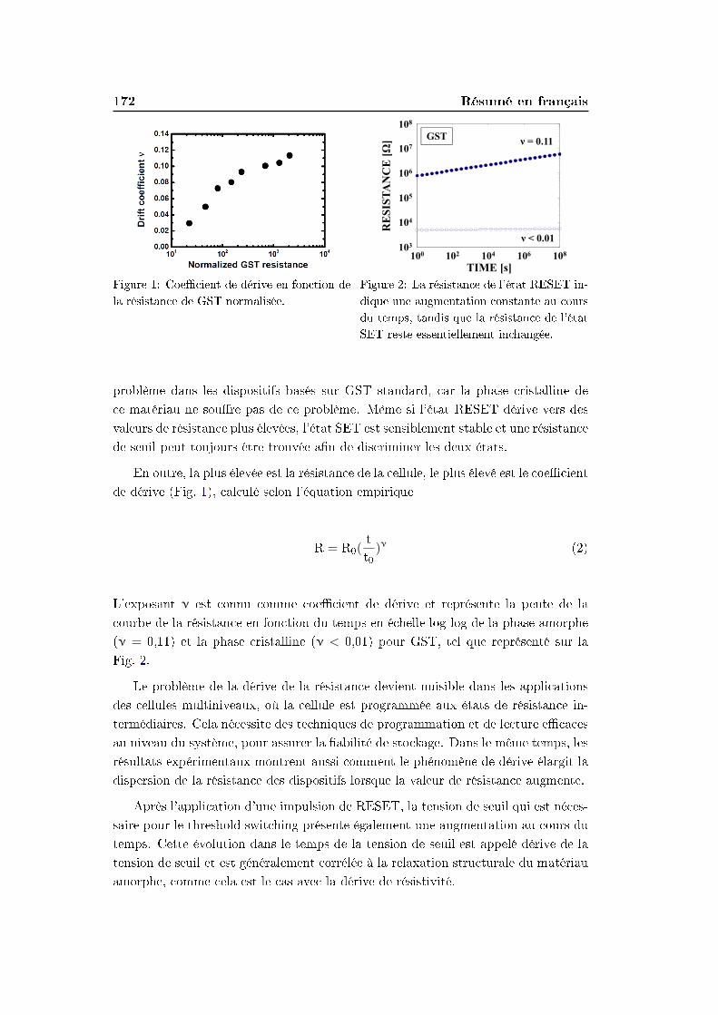
172 Résumé en français
Figure 1: Coecient de dérive en fonction de
la résistance de GST normalisée.
102 104 106
104
105
106
107
103
RE
SIST
AN
CE
[Ω]
TIME [s]108100
GST108
ν = 0.11
ν < 0.01
Figure 2: La résistance de l'état RESET in-
dique une augmentation constante au cours
du temps, tandis que la résistance de l'état
SET reste essentiellement inchangée.
problème dans les dispositifs basés sur GST standard, car la phase cristalline de
ce matériau ne soure pas de ce problème. Même si l'état RESET dérive vers des
valeurs de résistance plus élevées, l'état SET est sensiblement stable et une résistance
de seuil peut toujours être trouvée an de discriminer les deux états.
En outre, la plus élevée est la résistance de la cellule, le plus élevé est le coecient
de dérive (Fig. 1), calculé selon l'équation empirique
R = R0(tt0)ν (2)
L'exposant ν est connu comme coecient de dérive et représente la pente de la
courbe de la résistance en fonction du temps en échelle log-log de la phase amorphe
(ν = 0,11) et la phase cristalline (ν < 0,01) pour GST, tel que représenté sur la
Fig. 2.
Le problème de la dérive de la résistance devient nuisible dans les applications
des cellules multiniveaux, où la cellule est programmée aux états de résistance in-
termédiaires. Cela nécessite des techniques de programmation et de lecture ecaces
au niveau du système, pour assurer la abilité de stockage. Dans le même temps, les
résultats expérimentaux montrent aussi comment le phénomène de dérive élargit la
dispersion de la résistance des dispositifs lorsque la valeur de résistance augmente.
Après l'application d'une impulsion de RESET, la tension de seuil qui est néces-
saire pour le threshold switching présente également une augmentation au cours du
temps. Cette évolution dans le temps de la tension de seuil est appelé dérive de la
tension de seuil et est généralement corrélée à la relaxation structurale du matériau
amorphe, comme cela est le cas avec la dérive de résistivité.
Matériaux à changement de phase innovants 173
Matériaux à changement de phase innovants
Les propriétés des matériaux à changement de phase sont connues pour avoir un
eet sur les paramètres du dispositif PCM tel que la température de cristallisation,
ayant un eet sur la rétention des données et la durée de vie, tandis que la résistivité
de la phase amorphe et de la phase cristalline, qui aecte le courant ou la tension
nécessaire pour programmer la cellule.
Ge2Sb2Te5 (GST) est considéré comme le matériau de chalcogénure de référence
pour des applications PCM standards. L'un des principaux goulets d'étranglement
du GST est sa faible température de cristallisation (150 C) qui le rend intrinsèque-
ment incapable de satisfaire les exigences de la norme de rétention des données à 85C pendant 10 ans.
Dans les dernières années, de nombreux eorts ont été déployés dans la recherche
de nouveaux matériaux et l'étude de leurs propriétés pour cibler des applications
automobiles, pour lesquelles la température de fonctionnement est de l'ordre de
150 C. Pour répondre à cette exigence, des approches diérentes au niveau matériau
sont possibles. Une première approche consiste principalement en modiant la st÷-
chiométrie du GST ou en ajoutant des dopants pour augmenter la stabilité de l'état
amorphe. Une autre solution consiste à rechercher des diérents matériaux avec une
température de cristallisation élevée.
La conception de matériaux à base de verre de chalcogénure utilisés dans des
applications de mémoire à changement de phase peut considérablement améliorer les
caractéristiques du dispositif mémoire. L'addition de dopants est un moyen ecace
de modier les caractéristiques des matériaux à changement de phase, entraînant
une optimisation de la performance globale de la technologie.
Les dopants peuvent avoir pour eet une amélioration des paramètres du maté-
riau pour les applications de mémoire. Les températures élevées de cristallisation
sont prévues d'améliorer la rétention des données et de permettre l'intégration du
matériau et du dispositif pour des applications à haute température, alors qu'une
résistivité augmentée de la phase amorphe et la phase cristalline peut réduire le
courant de la programmation et la consommation.
La st÷chiométrie du GST peut être conçue pour augmenter sa température de
cristallisation et améliorer la stabilité thermique de la cellule de mémoire à change-
ment de phase. Le dopage à l'azote et au carbone entraîne une réduction du courant
de programmation, ce qui entraîne une consommation d'énergie réduite. En outre,
il a été démontré récemment que l'enrichissement du GST avec Ge augmente la
température de cristallisation du matériau, aux dépens de la réduction de la vitesse
de programmation SET.
An d'étudier et de comprendre le comportement des dispositifs basés sur GST
enrichi en Ge, nous avons eectué une série de mesures électriques sur ce matériau,
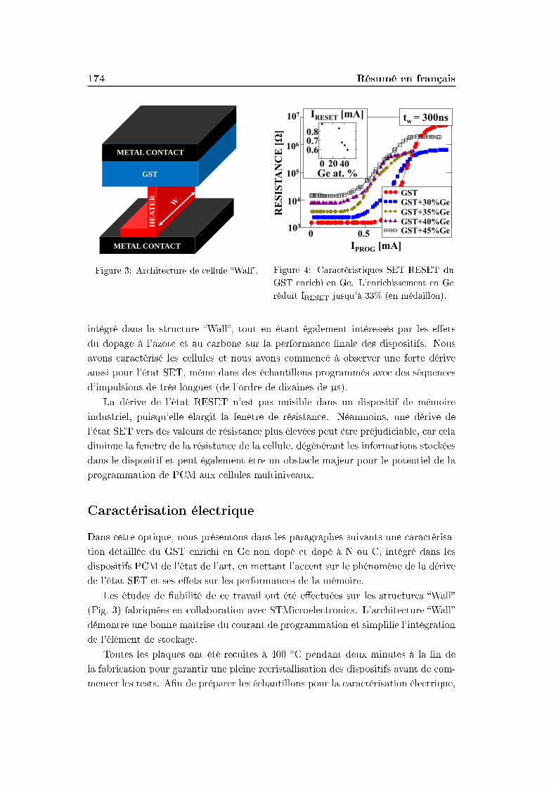
174 Résumé en français
METAL CONTACT
METAL CONTACT
GST
HE
AT
ER
METAL CONTACT
Figure 3: Architecture de cellule Wall.
0 0.5 1.0
105
IPROG [mA]
RE
SIS
TA
NC
E [Ω
]
tw = 300ns
104
103
106
107
GSTGST+30%Ge
GST+35%Ge
GST+40%GeGST+45%Ge
0 20 40
0.60.70.8
Ge at. %
IRESET [mA]107
Figure 4: Caractéristiques SET-RESET du
GST enrichi en Ge. L'enrichissement en Ge
réduit IRESET jusqu'à 33% (en médaillon).
intégré dans la structure Wall, tout en étant également intéressés par les eets
du dopage à l'azote et au carbone sur la performance nale des dispositifs. Nous
avons caractérisé les cellules et nous avons commencé à observer une forte dérive
aussi pour l'état SET, même dans des échantillons programmés avec des séquences
d'impulsions de très longues (de l'ordre de dizaines de µs).
La dérive de l'état RESET n'est pas nuisible dans un dispositif de mémoire
industriel, puisqu'elle élargit la fenêtre de résistance. Néanmoins, une dérive de
l'état SET vers des valeurs de résistance plus élevées peut être préjudiciable, car cela
diminue la fenêtre de la résistance de la cellule, dégénérant les informations stockées
dans le dispositif et peut également être un obstacle majeur pour le potentiel de la
programmation de PCM aux cellules multiniveaux.
Caractérisation électrique
Dans cette optique, nous présentons dans les paragraphes suivants une caractérisa-
tion détaillée du GST enrichi en Ge non dopé et dopé à N ou C, intégré dans les
dispositifs PCM de l'état de l'art, en mettant l'accent sur le phénomène de la dérive
de l'état SET et ses eets sur les performances de la mémoire.
Les études de abilité de ce travail ont été eectuées sur les structures Wall
(Fig. 3) fabriquées en collaboration avec STMicroelectronics. L'architecture Wall
démontre une bonne maîtrise du courant de programmation et simplie l'intégration
de l'élément de stockage.
Toutes les plaques ont été recuites à 400 C pendant deux minutes à la n de
la fabrication pour garantir une pleine recristallisation des dispositifs avant de com-
mencer les tests. An de préparer les échantillons pour la caractérisation électrique,
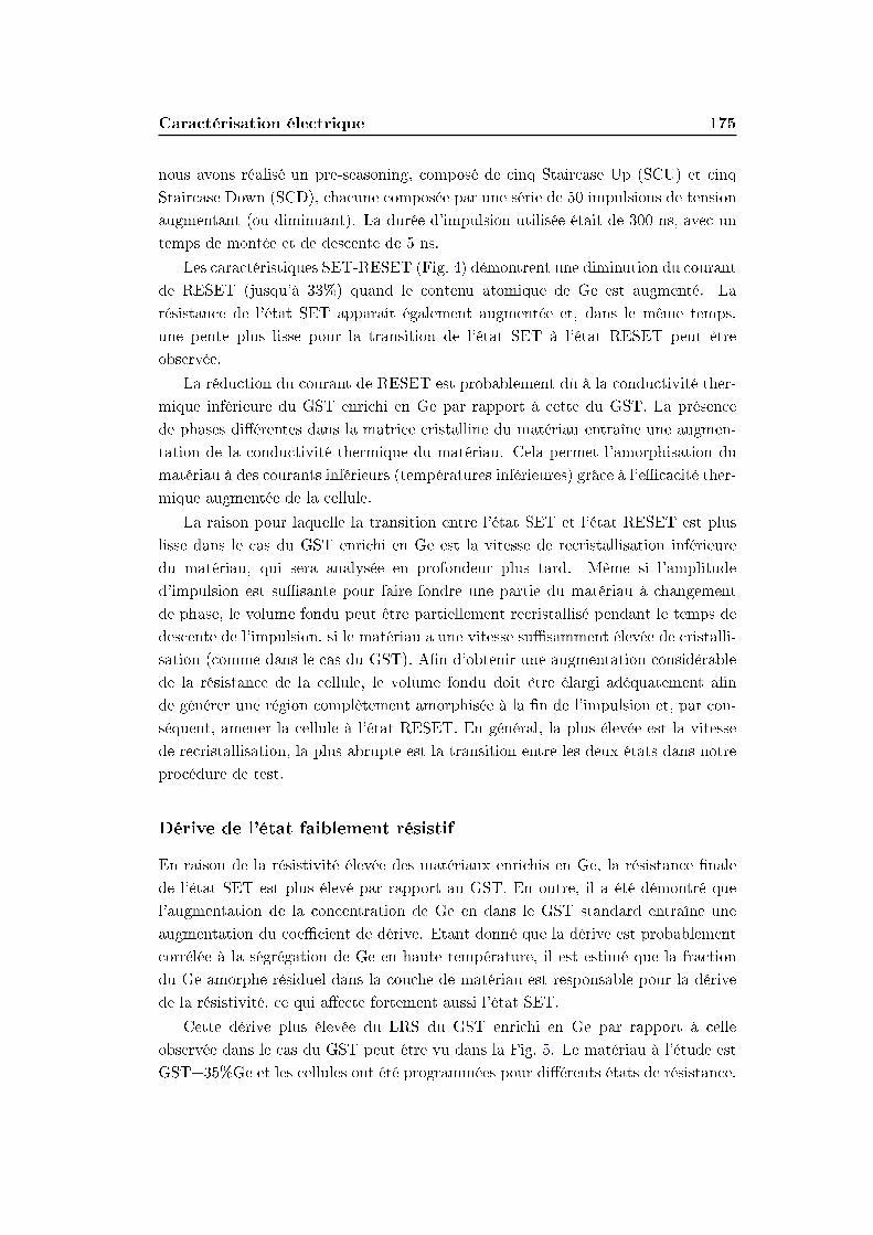
Caractérisation électrique 175
nous avons réalisé un pre-seasoning, composé de cinq Staircase Up (SCU) et cinq
Staircase Down (SCD), chacune composée par une série de 50 impulsions de tension
augmentant (ou diminuant). La durée d'impulsion utilisée était de 300 ns, avec un
temps de montée et de descente de 5 ns.
Les caractéristiques SET-RESET (Fig. 4) démontrent une diminution du courant
de RESET (jusqu'à 33%) quand le contenu atomique de Ge est augmenté. La
résistance de l'état SET apparaît également augmentée et, dans le même temps,
une pente plus lisse pour la transition de l'état SET à l'état RESET peut être
observée.
La réduction du courant de RESET est probablement dû à la conductivité ther-
mique inférieure du GST enrichi en Ge par rapport à cette du GST. La présence
de phases diérentes dans la matrice cristalline du matériau entraîne une augmen-
tation de la conductivité thermique du matériau. Cela permet l'amorphisation du
matériau à des courants inférieurs (températures inférieures) grâce à l'ecacité ther-
mique augmentée de la cellule.
La raison pour laquelle la transition entre l'état SET et l'état RESET est plus
lisse dans le cas du GST enrichi en Ge est la vitesse de recristallisation inférieure
du matériau, qui sera analysée en profondeur plus tard. Même si l'amplitude
d'impulsion est susante pour faire fondre une partie du matériau à changement
de phase, le volume fondu peut être partiellement recristallisé pendant le temps de
descente de l'impulsion, si le matériau a une vitesse susamment élevée de cristalli-
sation (comme dans le cas du GST). An d'obtenir une augmentation considérable
de la résistance de la cellule, le volume fondu doit être élargi adéquatement an
de générer une région complètement amorphisée à la n de l'impulsion et, par con-
séquent, amener la cellule à l'état RESET. En général, la plus élevée est la vitesse
de recristallisation, la plus abrupte est la transition entre les deux états dans notre
procédure de test.
Dérive de l'état faiblement résistif
En raison de la résistivité élevée des matériaux enrichis en Ge, la résistance nale
de l'état SET est plus élevé par rapport au GST. En outre, il a été démontré que
l'augmentation de la concentration de Ge en dans le GST standard entraîne une
augmentation du coecient de dérive. Etant donné que la dérive est probablement
corrélée à la ségrégation de Ge en haute température, il est estimé que la fraction
du Ge amorphe résiduel dans la couche de matériau est responsable pour la dérive
de la résistivité, ce qui aecte fortement aussi l'état SET.
Cette dérive plus élevée du LRS du GST enrichi en Ge par rapport à celle
observée dans le cas du GST peut être vu dans la Fig. 5. Le matériau à l'étude est
GST+35%Ge et les cellules ont été programmées pour diérents états de résistance.
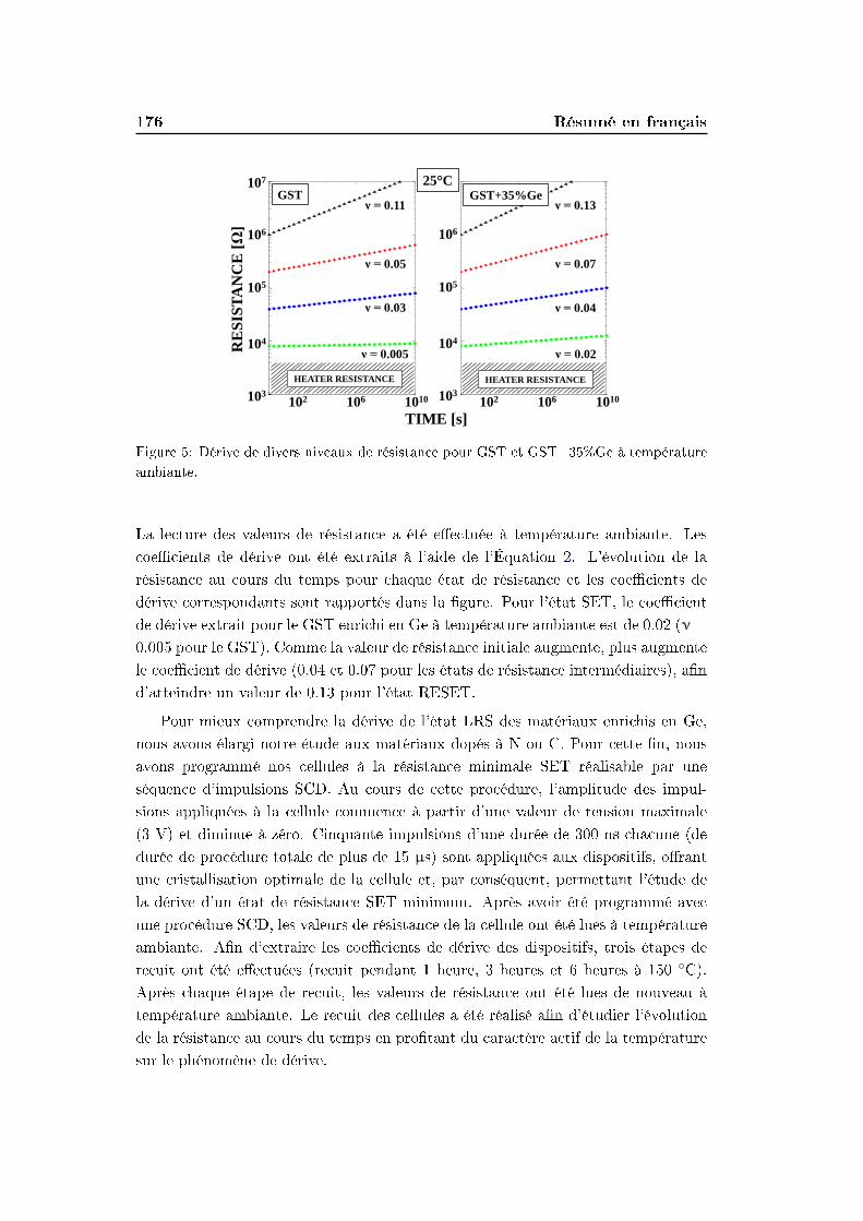
176 Résumé en français
100
102
104
106
108
1010
103
104
105
106
107
100
102
104
106
108
1010
103
104
105
106
107
GST+35%Ge107
106
105
104
103
107
106
105
104
103102 106 1010 102 106 1010
GST
TIME [s]
RE
SIS
TA
NC
E [
Ω]
HEATER RESISTANCE HEATER RESISTANCE
ν = 0.11
ν = 0.005
ν = 0.05
ν = 0.03
ν = 0.13
ν = 0.07
ν = 0.04
ν = 0.02
25°C
Figure 5: Dérive de divers niveaux de résistance pour GST et GST+35%Ge à température
ambiante.
La lecture des valeurs de résistance a été eectuée à température ambiante. Les
coecients de dérive ont été extraits à l'aide de l'Équation 2. L'évolution de la
résistance au cours du temps pour chaque état de résistance et les coecients de
dérive correspondants sont rapportés dans la gure. Pour l'état SET, le coecient
de dérive extrait pour le GST enrichi en Ge à température ambiante est de 0.02 (ν =
0.005 pour le GST). Comme la valeur de résistance initiale augmente, plus augmente
le coecient de dérive (0.04 et 0.07 pour les états de résistance intermédiaires), an
d'atteindre un valeur de 0.13 pour l'état RESET.
Pour mieux comprendre la dérive de l'état LRS des matériaux enrichis en Ge,
nous avons élargi notre étude aux matériaux dopés à N ou C. Pour cette n, nous
avons programmé nos cellules à la résistance minimale SET réalisable par une
séquence d'impulsions SCD. Au cours de cette procédure, l'amplitude des impul-
sions appliquées à la cellule commence à partir d'une valeur de tension maximale
(3 V) et diminue à zéro. Cinquante impulsions d'une durée de 300 ns chacune (de
durée de procédure totale de plus de 15 µs) sont appliquées aux dispositifs, orant
une cristallisation optimale de la cellule et, par conséquent, permettant l'étude de
la dérive d'un état de résistance SET minimum. Après avoir été programmé avec
une procédure SCD, les valeurs de résistance de la cellule ont été lues à température
ambiante. An d'extraire les coecients de dérive des dispositifs, trois étapes de
recuit ont été eectuées (recuit pendant 1 heure, 3 heures et 6 heures à 150 C).
Après chaque étape de recuit, les valeurs de résistance ont été lues de nouveau à
température ambiante. Le recuit des cellules a été réalisé an d'étudier l'évolution
de la résistance au cours du temps en protant du caractère actif de la température
sur le phénomène de dérive.
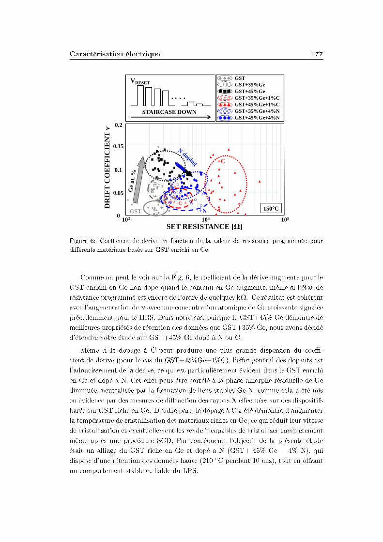
Caractérisation électrique 177
150°C
+C
+N GST
GST
GST+35%Ge
GST+45%Ge
GST+35%Ge+1%C
GST+45%Ge+1%C
GST+35%Ge+4%N
GST+45%Ge+4%N
103 104 105 0
0.05
0.1
0.15
SET RESISTANCE [Ω]
DR
IFT
CO
EF
FIC
IEN
T v
+C
0.2
STAIRCASE DOWN
VRESET
Figure 6: Coecient de dérive en fonction de la valeur de résistance programmée pour
diérents matériaux basés sur GST enrichi en Ge.
Comme on peut le voir sur la Fig. 6, le coecient de la dérive augmente pour le
GST enrichi en Ge non dope quand le contenu en Ge augmente, même si l'état de
résistance programmé est encore de l'ordre de quelques kΩ. Ce résultat est cohérent
avec l'augmentation de ν avec une concentration atomique de Ge croissante signalée
précédemment pour le HRS. Dans notre cas, puisque le GST+45% Ge démontre de
meilleures propriétés de rétention des données que GST+35% Ge, nous avons décidé
d'étendre notre étude sur GST+45% Ge dopé à N ou C.
Même si le dopage à C peut produire une plus grande dispersion du coe-
cient de dérive (pour le cas du GST+45%Ge+1%C), l'eet général des dopants est
l'adoucissement de la dérive, ce qui est particulièrement évident dans le GST enrichi
en Ge et dopé a N. Cet eet peut être corrélé à la phase amorphe résiduelle de Ge
diminuée, neutralisée par la formation de liens stables Ge-N, comme cela a été mis
en évidence par des mesures de diraction des rayons X eectuées sur des dispositifs
basés sur GST riche en Ge. D'autre part, le dopage à C a été démontré d'augmenter
la température de cristallisation des matériaux riches en Ge, ce qui réduit leur vitesse
de cristallisation et éventuellement les rende incapables de cristalliser complètement
même après une procédure SCD. Par conséquent, l'objectif de la présente étude
était un alliage du GST riche en Ge et dopé a N (GST+ 45% Ge + 4% N), qui
dispose d'une rétention des données haute (210 C pendant 10 ans), tout en orant
un comportement stable et able du LRS.
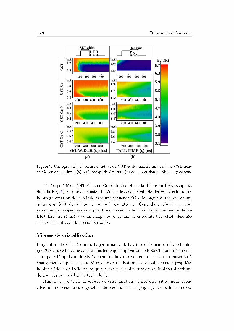
178 Résumé en français
GS
T-G
e-N
G
ST
-Ge-
C
log10(R)
SET WIDTH (tw) [ns] FALL TIME (tf) [ns]
SET width fall time
6.7
6.3
5.9
5.5
5.1
4.7
4.3
3.9
3.5
3.1
1.0
0.5
100 200 300 400
1.0
0.5
200 400 600 800
0.8
0.6 0.4
0.9
0.7
0.5 200 400 600 800
0.8 0.6 0.4
0.8 0.6 0.4
0.8 0.6 0.4
0.8 0.6 0.4
[mA] [mA]
[mA] [mA]
[mA]
[mA] [mA]
[mA]
GS
T-G
e G
ST
200 400 600 800
200 400 600 800
200 400 600 800
200 400 600 800
200 400 600 800
(a) (b)
Figure 7: Cartographies de recristallisation du GST et des matériaux basés sur GST riche
en Ge lorsque la durée (a) ou le temps de descente (b) de l'impulsion de SET augmentent.
L'eet positif du GST riche en Ge et dopé à N sur la dérive du LRS, rapporté
dans la Fig. 6, est une conclusion basée sur les coecients de dérive extraits après
la programmation de la cellule avec une séquence SCD de longue durée, qui assure
qu'un état SET de résistance minimale est atteint. Cependant, an de pouvoir
répondre aux exigences des applications nales, ce bon résultat en termes de dérive
LRS doit être réalisé avec un temps de programmation réduit. Une étude destinée
à cet eet suit dans la section suivante.
Vitesse de cristallisation
L'opération de SET détermine la performance de la vitesse d'écriture de la technolo-
gie PCM, car elle est beaucoup plus lente que l'opération de RESET. La durée néces-
saire pour l'impulsion de SET dépend de la vitesse de cristallisation du matériau à
changement de phase. Cette vitesse de cristallisation est probablement la propriété
la plus critique de PCM parce qu'elle xe une limite supérieure du débit d'écriture
de données potentiel de la technologie.
An de caractériser la vitesse de cristallisation de nos dispositifs, nous avons
eectué une série de cartographies de recristallisation (Fig. 7). Les cellules ont été
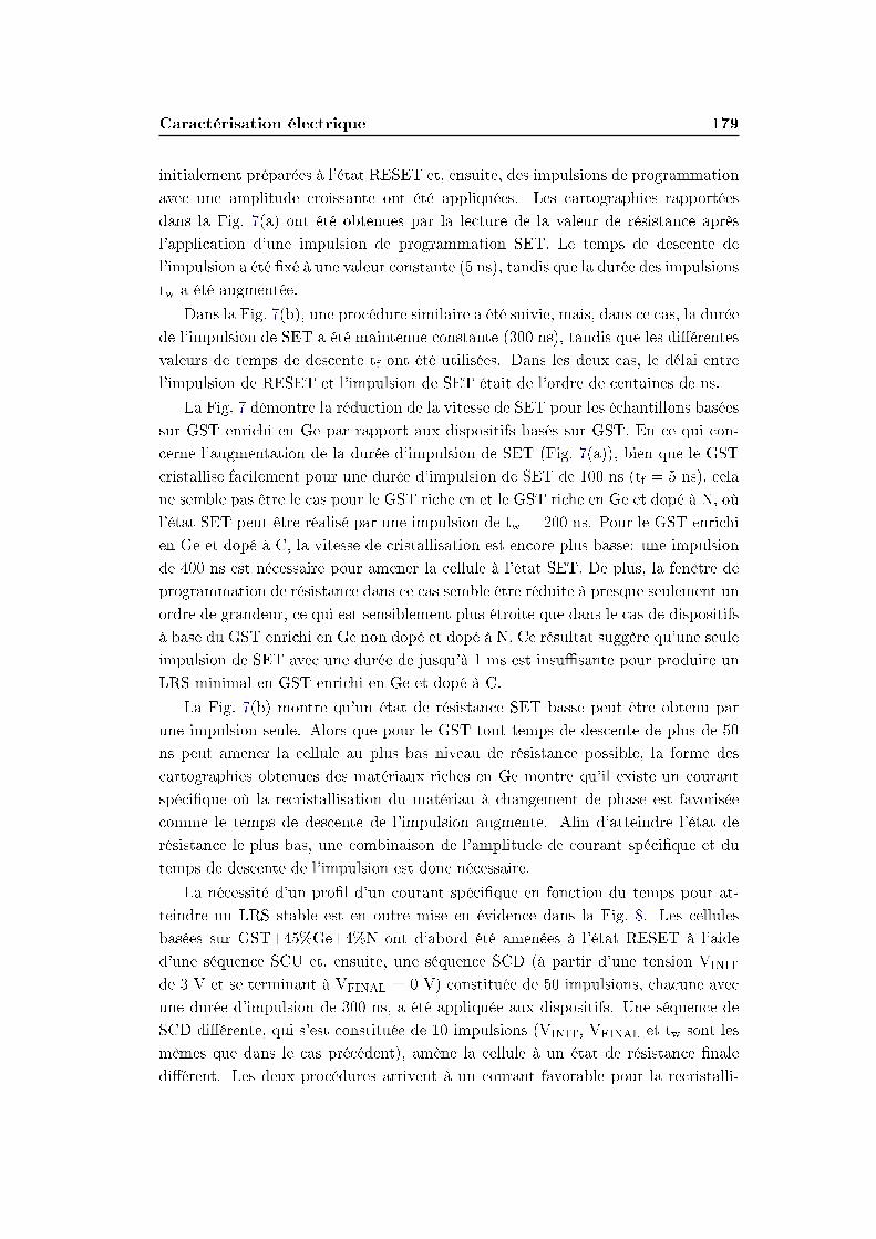
Caractérisation électrique 179
initialement préparées à l'état RESET et, ensuite, des impulsions de programmation
avec une amplitude croissante ont été appliquées. Les cartographies rapportées
dans la Fig. 7(a) ont été obtenues par la lecture de la valeur de résistance après
l'application d'une impulsion de programmation SET. Le temps de descente de
l'impulsion a été xé à une valeur constante (5 ns), tandis que la durée des impulsions
tw a été augmentée.
Dans la Fig. 7(b), une procédure similaire a été suivie, mais, dans ce cas, la durée
de l'impulsion de SET a été maintenue constante (300 ns), tandis que les diérentes
valeurs de temps de descente tf ont été utilisées. Dans les deux cas, le délai entre
l'impulsion de RESET et l'impulsion de SET était de l'ordre de centaines de ns.
La Fig. 7 démontre la réduction de la vitesse de SET pour les échantillons basées
sur GST enrichi en Ge par rapport aux dispositifs basés sur GST. En ce qui con-
cerne l'augmentation de la durée d'impulsion de SET (Fig. 7(a)), bien que le GST
cristallise facilement pour une durée d'impulsion de SET de 100 ns (tf = 5 ns), cela
ne semble pas être le cas pour le GST riche en et le GST riche en Ge et dopé à N, où
l'état SET peut être réalisé par une impulsion de tw = 200 ns. Pour le GST enrichi
en Ge et dopé à C, la vitesse de cristallisation est encore plus basse: une impulsion
de 400 ns est nécessaire pour amener la cellule à l'état SET. De plus, la fenêtre de
programmation de résistance dans ce cas semble être réduite à presque seulement un
ordre de grandeur, ce qui est sensiblement plus étroite que dans le cas de dispositifs
à base du GST enrichi en Ge non dopé et dopé à N. Ce résultat suggère qu'une seule
impulsion de SET avec une durée de jusqu'à 1 ms est insusante pour produire un
LRS minimal en GST enrichi en Ge et dopé à C.
La Fig. 7(b) montre qu'un état de résistance SET basse peut être obtenu par
une impulsion seule. Alors que pour le GST tout temps de descente de plus de 50
ns peut amener la cellule au plus bas niveau de résistance possible, la forme des
cartographies obtenues des matériaux riches en Ge montre qu'il existe un courant
spécique où la recristallisation du matériau à changement de phase est favorisée
comme le temps de descente de l'impulsion augmente. An d'atteindre l'état de
résistance le plus bas, une combinaison de l'amplitude de courant spécique et du
temps de descente de l'impulsion est donc nécessaire.
La nécessité d'un prol d'un courant spécique en fonction du temps pour at-
teindre un LRS stable est en outre mise en évidence dans la Fig. 8. Les cellules
basées sur GST+45%Ge+4%N ont d'abord été amenées à l'état RESET à l'aide
d'une séquence SCU et, ensuite, une séquence SCD (à partir d'une tension VINIT
de 3 V et se terminant à VFINAL = 0 V) constituée de 50 impulsions, chacune avec
une durée d'impulsion de 300 ns, a été appliquée aux dispositifs. Une séquence de
SCD diérente, qui s'est constituée de 10 impulsions (VINIT, VFINAL et tw sont les
mêmes que dans le cas précédent), amène la cellule à un état de résistance nale
diérent. Les deux procédures arrivent à un courant favorable pour la recristalli-
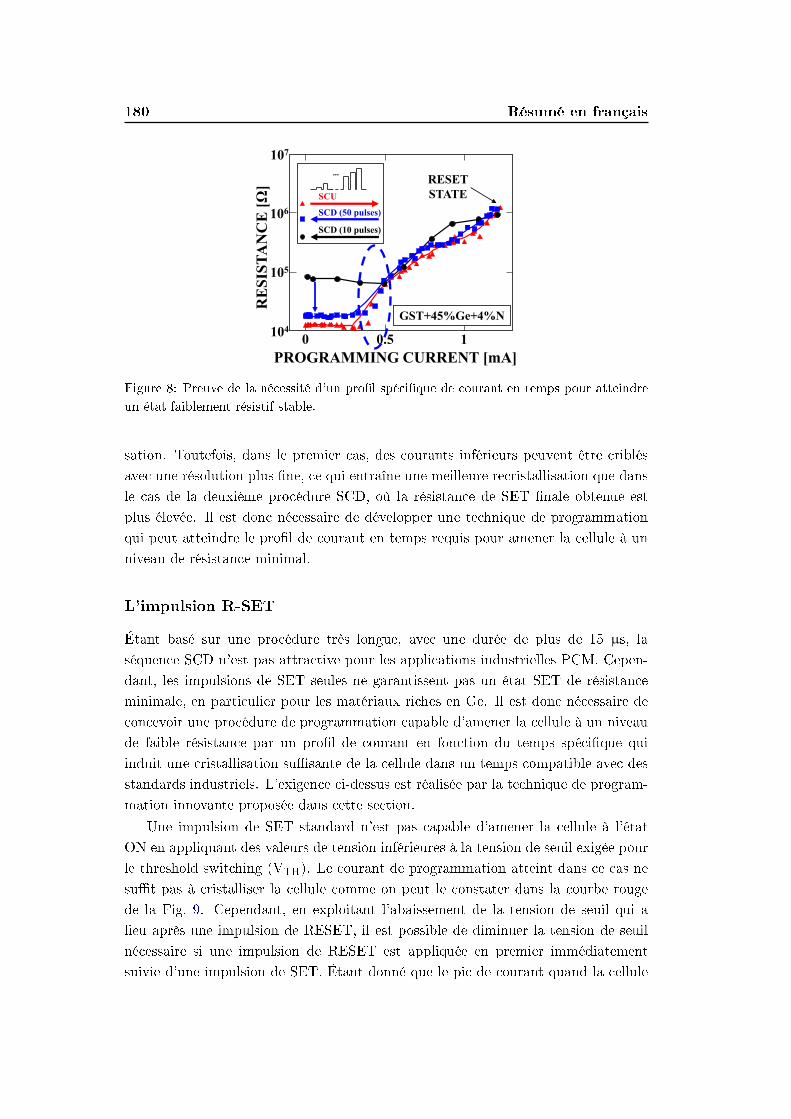
180 Résumé en français
0 0.5 1104
105
106
107
PROGRAMMING CURRENT [mA]
RE
SIS
TA
NC
E [Ω
]
RESET
STATE
GST+45%Ge+4%N
...
SCU
SCD (50 pulses)
SCD (10 pulses)
Figure 8: Preuve de la nécessité d'un prol spécique de courant en temps pour atteindre
un état faiblement résistif stable.
sation. Toutefois, dans le premier cas, des courants inférieurs peuvent être criblés
avec une résolution plus ne, ce qui entraîne une meilleure recristallisation que dans
le cas de la deuxième procédure SCD, où la résistance de SET nale obtenue est
plus élevée. Il est donc nécessaire de développer une technique de programmation
qui peut atteindre le prol de courant en temps requis pour amener la cellule à un
niveau de résistance minimal.
L'impulsion R-SET
Étant basé sur une procédure très longue, avec une durée de plus de 15 µs, la
séquence SCD n'est pas attractive pour les applications industrielles PCM. Cepen-
dant, les impulsions de SET seules ne garantissent pas un état SET de résistance
minimale, en particulier pour les matériaux riches en Ge. Il est donc nécessaire de
concevoir une procédure de programmation capable d'amener la cellule à un niveau
de faible résistance par un prol de courant en fonction du temps spécique qui
induit une cristallisation susante de la cellule dans un temps compatible avec des
standards industriels. L'exigence ci-dessus est réalisée par la technique de program-
mation innovante proposée dans cette section.
Une impulsion de SET standard n'est pas capable d'amener la cellule à l'état
ON en appliquant des valeurs de tension inférieures à la tension de seuil exigée pour
le threshold switching (VTH). Le courant de programmation atteint dans ce cas ne
sut pas à cristalliser la cellule comme on peut le constater dans la courbe rouge
de la Fig. 9. Cependant, en exploitant l'abaissement de la tension de seuil qui a
lieu après une impulsion de RESET, il est possible de diminuer la tension de seuil
nécessaire si une impulsion de RESET est appliquée en premier immédiatement
suivie d'une impulsion de SET. Étant donné que le pic de courant quand la cellule
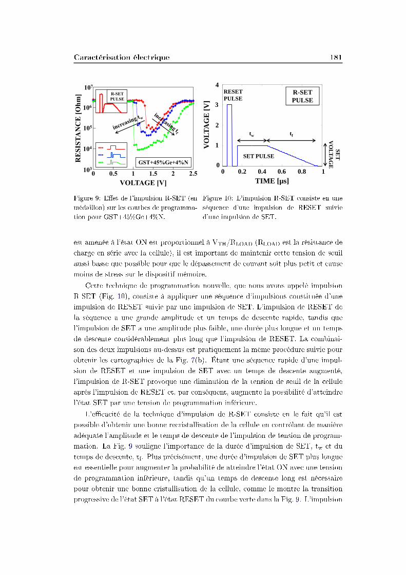
Caractérisation électrique 181
0 0.5 1 1.5 2 2.5103
VOLTAGE [V]
RE
SIS
TA
NC
E [
Oh
m]
104
105
106
107
R-SET
PULSE
GST+45%Ge+4%N
Figure 9: Eet de l'impulsion R-SET (en
médaillon) sur les courbes de programma-
tion pour GST+45%Ge+4%N.
tw tf
SET PULSE
R-SET PULSE
SE
T
VO
LTAG
E
VO
LTA
GE
[V]
1
2
3
4
0 0.2 0.4 0.6 0.8 1
TIME [µs]
0
RESET PULSE
Figure 10: L'impulsion R-SET consiste en une
séquence d'une impulsion de RESET suivie
d'une impulsion de SET.
est amenée à l'état ON est proportionnel à VTH/RLOAD (RLOAD est la résistance de
charge en série avec la cellule), il est important de maintenir cette tension de seuil
aussi basse que possible pour que le dépassement de courant soit plus petit et cause
moins de stress sur le dispositif mémoire.
Cette technique de programmation nouvelle, que nous avons appelé impulsion
R-SET (Fig. 10), consiste à appliquer une séquence d'impulsions constituée d'une
impulsion de RESET suivie par une impulsion de SET. L'impulsion de RESET de
la séquence a une grande amplitude et un temps de descente rapide, tandis que
l'impulsion de SET a une amplitude plus faible, une durée plus longue et un temps
de descente considérablement plus long que l'impulsion de RESET. La combinai-
son des deux impulsions au-dessus est pratiquement la même procédure suivie pour
obtenir les cartographies de la Fig. 7(b). Étant une séquence rapide d'une impul-
sion de RESET et une impulsion de SET avec un temps de descente augmenté,
l'impulsion de R-SET provoque une diminution de la tension de seuil de la cellule
après l'impulsion de RESET et, par conséquent, augmente la possibilité d'atteindre
l'état SET par une tension de programmation inférieure.
L'ecacité de la technique d'impulsion de R-SET consiste en le fait qu'il est
possible d'obtenir une bonne recristallisation de la cellule en contrôlant de manière
adéquate l'amplitude et le temps de descente de l'impulsion de tension de program-
mation. La Fig. 9 souligne l'importance de la durée d'impulsion de SET, tw et du
temps de descente, tf. Plus précisément, une durée d'impulsion de SET plus longue
est essentielle pour augmenter la probabilité de atteindre l'état ON avec une tension
de programmation inférieure, tandis qu'un temps de descente long est nécessaire
pour obtenir une bonne cristallisation de la cellule, comme le montre la transition
progressive de l'état SET à l'état RESET du courbe verte dans la Fig. 9. L'impulsion
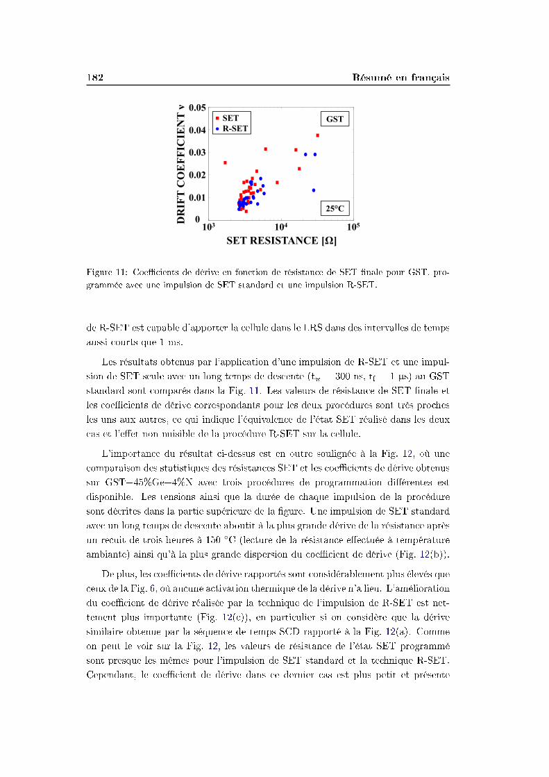
182 Résumé en français
SET RESISTANCE [Ω]
DR
IFT
CO
EFF
ICIE
NT
ν
GST
25°C
103 104 1050
0.01
0.05
0.02
0.04
0.03
SETR-SET
Figure 11: Coecients de dérive en fonction de résistance de SET nale pour GST, pro-
grammée avec une impulsion de SET standard et une impulsion R-SET.
de R-SET est capable d'apporter la cellule dans le LRS dans des intervalles de temps
aussi courts que 1 ms.
Les résultats obtenus par l'application d'une impulsion de R-SET et une impul-
sion de SET seule avec un long temps de descente (tw = 300 ns, tf = 1 µs) au GST
standard sont comparés dans la Fig. 11. Les valeurs de résistance de SET nale et
les coecients de dérive correspondants pour les deux procédures sont très proches
les uns aux autres, ce qui indique l'équivalence de l'état SET réalisé dans les deux
cas et l'eet non nuisible de la procédure R-SET sur la cellule.
L'importance du résultat ci-dessus est en outre soulignée à la Fig. 12, où une
comparaison des statistiques des résistances SET et les coecients de dérive obtenus
sur GST+45%Ge+4%N avec trois procédures de programmation diérentes est
disponible. Les tensions ainsi que la durée de chaque impulsion de la procédure
sont décrites dans la partie supérieure de la gure. Une impulsion de SET standard
avec un long temps de descente aboutit à la plus grande dérive de la résistance après
un recuit de trois heures à 150 C (lecture de la résistance eectuée à température
ambiante) ainsi qu'à la plus grande dispersion du coecient de dérive (Fig. 12(b)).
De plus, les coecients de dérive rapportés sont considérablement plus élevés que
ceux de la Fig. 6, où aucune activation thermique de la dérive n'a lieu. L'amélioration
du coecient de dérive réalisée par la technique de l'impulsion de R-SET est net-
tement plus importante (Fig. 12(c)), en particulier si on considère que la dérive
similaire obtenue par la séquence de temps SCD rapporté à la Fig. 12(a). Comme
on peut le voir sur la Fig. 12, les valeurs de résistance de l'état SET programmé
sont presque les mêmes pour l'impulsion de SET standard et la technique R-SET.
Cependant, le coecient de dérive dans ce dernier cas est plus petit et présente
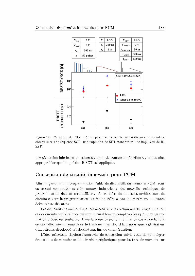
Conception de circuits innovants pour PCM 183
104
105
RE
SIS
TA
NC
E [Ω
]
0.2
0.4
DR
IFT
CO
EF
FIC
IEN
T
GST+45%Ge+4%N
(a) (b) (c)
LRS
After 3h at 150°C
Vinit 3 V
Vfinal 0 V
tw 300 ns
n 50 pulses
VSET 1.2 V
VRESET 3 V
tw,RESET 50 ns
tw,SET 300 ns
tf,SET 500 ns
V 1.5 V
tw 300 ns
tf 1 µs
Figure 12: Résistance de l'état SET programmée et coecient de dérive correspondant
obtenu avec une séquence SCD, une impulsion de SET standard et une impulsion de R-
SET.
une dispersion inférieure, en raison du prol de courant en fonction du temps plus
approprié lorsque l'impulsion R-SET est appliquée.
Conception de circuits innovants pour PCM
An de garantir une programmation able de dispositifs de mémoire PCM, tout
en restant compatible avec les normes industrielles, des nouvelles techniques de
programmation doivent être utilisées. A cet eet, de nouvelles architectures de
circuits ciblant la programmation précise de PCM à base de matériaux innovants
doivent être discutées.
Les dispositifs de mémoire avancés nécessitent des techniques de programmation
et des circuits périphériques qui sont inévitablement complexes lorsqu'une program-
mation précise est souhaitée. Dans la présente section, la mise en ÷uvre de la con-
ception eectuée au cours de cette étude est discutée. Il faut noter que le générateur
d'impulsions développé est destiné aux ns de caractérisation.
L'idée principale derrière l'approche de conception suivie était de co-intégrer
des cellules de mémoire et des circuits périphériques pour les tests de mémoire sur

184 Résumé en français
FEOL + BEOL (foundry)- 4 Cu layers- 130 nm CMOS technology
Final deposition (LETI)- 1 – 2 metal layers + PCM structures- 50 nm (e-beam)/ 300 nm (DUV) technology
Figure 13: Schéma des couches métalliques CMOS (circuit de programmation) et des
couches d'éléments de mémoire (couches 5 - 6).
la même plaque, avec les couches métalliques 1 à 4 utilisées pour la partie BEOL
(circuits) et les couches métalliques 5 et au-dessus dédiées au dépôt des éléments de
changement de phase, comme représenté sur la Fig. 13.
Pour cette mise en ÷uvre, nous avons utilisé des cellules de hauteur standard
(7.26 µm). Une technologie de 130 nm CMOS de STMicroelectronics a été utilisée et
une ligne de scribe de 25-pads a été mise à disposition pour les signaux des circuits
I/O.
En raison des dicultés de génération des courants externes par l'équipement de
caractérisation, l'approche suivie était de générer en interne tous les courants requis.
En outre, les courants qui contrôlent la pente de descente de l'impulsion de SET
générée sont programmés numériquement par des tensions externes. Cette méthode
présente l'inconvénient d'inexactitude potentielle des courants générés en raison des
écarts de processus de fabrication et des variations de conditions de fonctionnement,
mais, comme cela sera décrit dans la suite, est capable de générer jusqu'à huit
pentes diérentes pour la pente de descente de l'impulsion de programmation SET,
couvrant ainsi les cas essentiels d'impulsions nécessaires pour la programmation du
PCM.
Même si la caractérisation de dispositifs de mémoire était l'objectif nal de cette
mise en ÷uvre, il n'a pas été possible d'intégrer les éléments de mémoire sur le dessus
de la couche métallique 4 en raison de contraintes liées au temps. Par conséquent,
l'eet de la programmation de la cellule de mémoire avec le circuit présenté dans les
paragraphes précédents ne pouvait pas être étudié expérimentalement. Toutefois,
dans la présente section, nous montrons la conception qui a été mis en ÷uvre et
la mise en page (le layout) du circuit développé. Les simulations post-layout sont
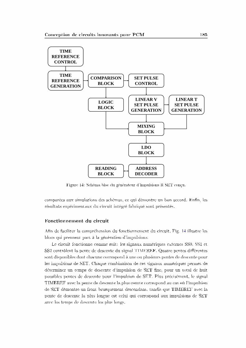
Conception de circuits innovants pour PCM 185
TIME REFERENCE
GENERATION
COMPARISON BLOCK
LOGICBLOCK
SET PULSE CONTROL
LINEAR V SET PULSE
GENERATION
LINEAR TSET PULSE
GENERATION
MIXING BLOCK
LDO BLOCK
ADDRESS DECODER
TIME REFERENCE
CONTROL
READINGBLOCK
Figure 14: Schéma-bloc du générateur d'impulsions R-SET conçu.
comparées aux simulations des schémas, ce qui démontre un bon accord. Enn, les
résultats expérimentaux du circuit intégré fabriqué sont présentés.
Fonctionnement du circuit
An de faciliter la compréhension du fonctionnement du circuit, Fig. 14 illustre les
blocs qui prennent part à la génération d'impulsions.
Le circuit fonctionne comme suit: les signaux numériques externes SS0, SS1 et
SS2 contrôlent la pente de descente du signal TIMEREF. Quatre pentes diérentes
sont disponibles dont chacune correspond à une ou plusieurs pentes de descente pour
les impulsions de SET. Chaque combinaison de ces signaux numériques permet de
déterminer un temps de descente d'impulsion de SET xe, pour un total de huit
possibles pentes de descente pour l'impulsion de SET. Plus précisément, le signal
TIMEREF avec la pente de descente la plus courte correspond au cas où l'impulsion
de SET démontre un front brusquement descendant, tandis que TIMEREF avec la
pente de descente la plus longue est celui qui correspond aux impulsions de SET
avec les temps de descente les plus longs.
186 Résumé en français
Le signal TIMEREF généré est ensuite amené à quatre comparateurs qui génèrent
des signaux numériques, qui, à leur tour sont portés au bloc de la logique et permet-
tent la génération de l'impulsion de SET. Sous le signal SEL, il est possible de choisir
entre une pente de descente diminuant linéairement ou une impulsion de tension in-
duisant un prol de température décroissant linéairement qui peut potentiellement
entraîner la croissance de cristaux dans la région active de la cellule de mémoire.
L'impulsion R-SET est obtenue au bloc de combinaison analogique et est en-
suite amenée au bloc de LDO, qui ore le courant nécessaire pour programmer les
cellules. Cinq signaux d'adressage permettent de sélectionner la cellule de PCM
d'être programmée par l'impulsion R-SET générée ou, à défaut, fournir l'impulsion
R-SET à un pad de sortie dédié au contrôle du signal amené aux éléments de mé-
moire. Un bloc de lecture de la valeur de résistance de la cellule PCM sélectionnée
est également inclus.
L'initialisation de l'impulsion est déclenchée par l'impulsion VTRIG. Les signaux
signaux externes SS0, SS1 et SS2 sont nécessaires pour contrôler la pente de descente
du TIMEREF. Ensuite, le signal TIMEREF est amené à une cascade de quatre
comparateurs pour le comparer à quatre référence externe tensions VREF,i (i = 1
à 4): la sortie de chaque comparateur est amenée à VDD une fois la valeur du
TIMEREF chute en dessous de la valeur de tension de référence correspondante.
Les signaux générés dans le bloc de comparaison sont en outre introduits dans le
bloc de logique, où les signaux qui permettent aux signaux de la tension de RESET,
de l'impulsion de SET, ainsi que le signal de masse, d'être amenés à la sortie du
circuit, sont générés. Le signal VSET,STOP est également amené au bloc où les
signaux numériques qui contrôlent la pente de descente de l'impulsion de SET sont
générés.
Il faut souligner que les mêmes signaux qui contrôlent la pente de descente du
signal TIMEREF contrôlent également la pente de descente de l'impulsion de SET.
Ce choix a été fait an d'être en mesure de générer des impulsions de SET de courte
durée quand un signal TIMEREF avec une pente de descente spécique a été généré.
Par exemple, an de générer une impulsion de SET avec une durée de 100 ns, les
tensions de référence nécessaires pour VREF,3 et VREF,4 doivent avoir une diérence
de tension de 1 V lorsque le signal TIMEREF a un taux de décharge de 5 V/500
ns (= 106 V/s), tandis que lorsque la pente de descente du TIMEREF correspond
à un taux de décharge de 107 V/s, la diérence de tension entre VREF,3 et VREF,4
est de 100 mV, ce qui peut être dicile à générer, donc la durée de l'impulsion de
SET générée ne sera pas bien contrôlée.
L'impulsion de SET générée est ensuite amenée au circuit de génération d'une
impulsion pour induire un prol de température diminuant linéairement. Les deux
impulsions de SET, notamment celle avec un front diminuant linéairement et celle
qui entraîne une diminution de température linéaire, sont introduites dans le bloc
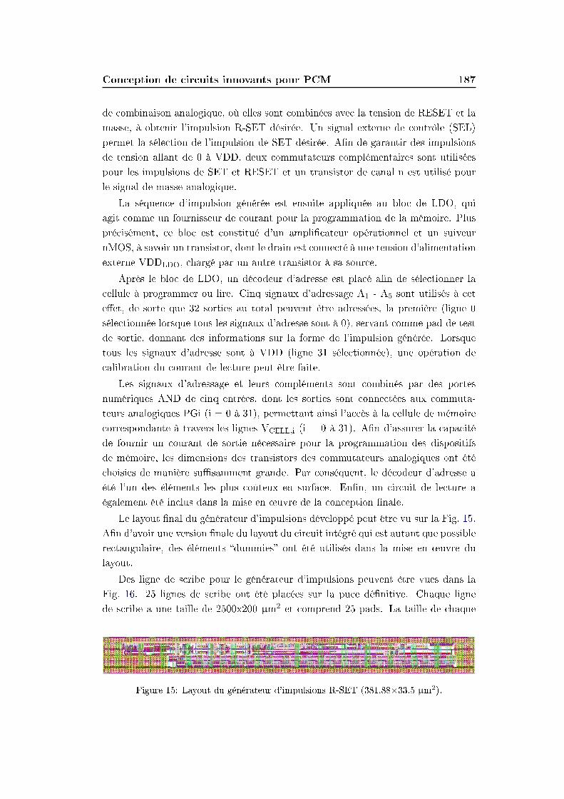
Conception de circuits innovants pour PCM 187
de combinaison analogique, où elles sont combinées avec la tension de RESET et la
masse, à obtenir l'impulsion R-SET désirée. Un signal externe de contrôle (SEL)
permet la sélection de l'impulsion de SET désirée. An de garantir des impulsions
de tension allant de 0 à VDD, deux commutateurs complémentaires sont utilisées
pour les impulsions de SET et RESET et un transistor de canal n est utilisé pour
le signal de masse analogique.
La séquence d'impulsion générée est ensuite appliquée au bloc de LDO, qui
agit comme un fournisseur de courant pour la programmation de la mémoire. Plus
précisément, ce bloc est constitué d'un amplicateur opérationnel et un suiveur
nMOS, à savoir un transistor, dont le drain est connecté à une tension d'alimentation
externe VDDLDO, chargé par un autre transistor à sa source.
Après le bloc de LDO, un décodeur d'adresse est placé an de sélectionner la
cellule à programmer ou lire. Cinq signaux d'adressage A1 - A5 sont utilisés à cet
eet, de sorte que 32 sorties au total peuvent être adressées, la première (ligne 0
sélectionnée lorsque tous les signaux d'adresse sont à 0), servant comme pad de test
de sortie, donnant des informations sur la forme de l'impulsion générée. Lorsque
tous les signaux d'adresse sont à VDD (ligne 31 sélectionnée), une opération de
calibration du courant de lecture peut être faite.
Les signaux d'adressage et leurs compléments sont combinés par des portes
numériques AND de cinq entrées, dont les sorties sont connectées aux commuta-
teurs analogiques PGi (i = 0 à 31), permettant ainsi l'accès à la cellule de mémoire
correspondante à travers les lignes VCELL,i (i = 0 à 31). An d'assurer la capacité
de fournir un courant de sortie nécessaire pour la programmation des dispositifs
de mémoire, les dimensions des transistors des commutateurs analogiques ont été
choisies de manière susamment grande. Par conséquent, le décodeur d'adresse a
été l'un des éléments les plus coûteux en surface. Enn, un circuit de lecture a
également été inclus dans la mise en ÷uvre de la conception nale.
Le layout nal du générateur d'impulsions développé peut être vu sur la Fig. 15.
An d'avoir une version nale du layout du circuit intégré qui est autant que possible
rectangulaire, des éléments dummies ont été utilisés dans la mise en ÷uvre du
layout.
Des ligne de scribe pour le générateur d'impulsions peuvent être vues dans la
Fig. 16. 25 lignes de scribe ont été placées sur la puce dénitive. Chaque ligne
de scribe a une taille de 2500x200 µm2 et comprend 25 pads. La taille de chaque
Figure 15: Layout du générateur d'impulsions R-SET (381.88×33.5 µm2).
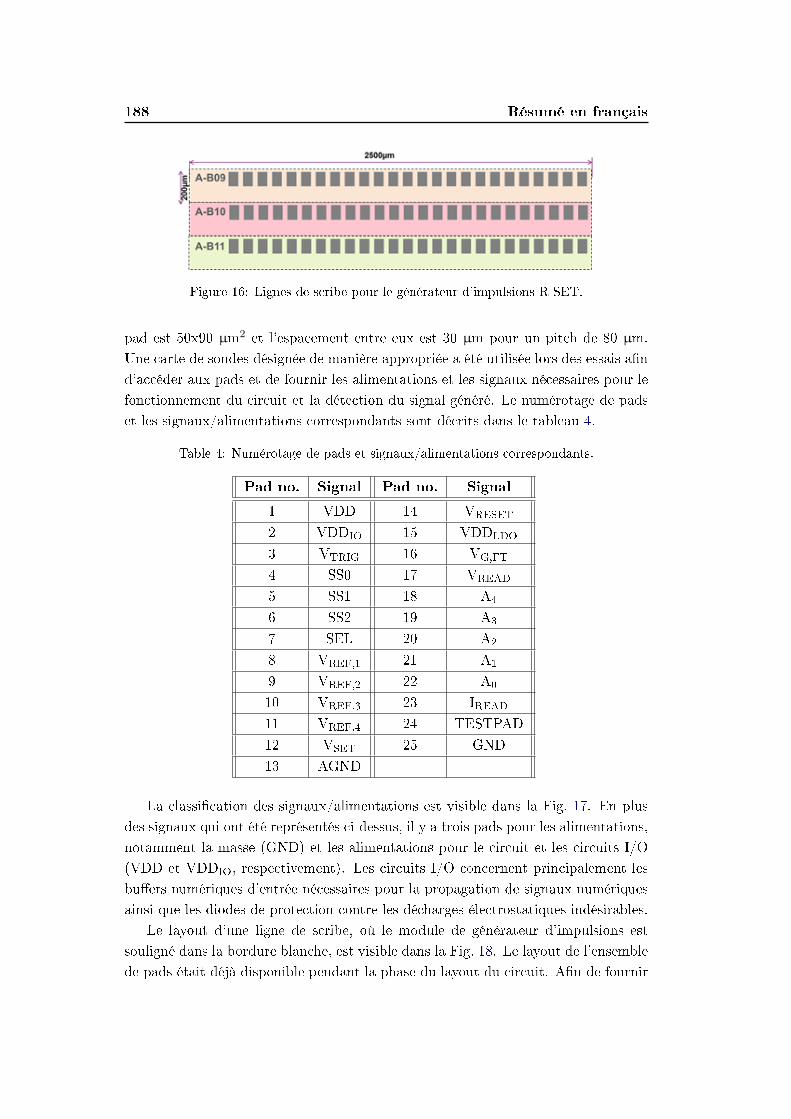
188 Résumé en français
Figure 16: Lignes de scribe pour le générateur d'impulsions R-SET.
pad est 50x90 µm2 et l'espacement entre eux est 30 µm pour un pitch de 80 µm.
Une carte de sondes désignée de manière appropriée a été utilisée lors des essais an
d'accéder aux pads et de fournir les alimentations et les signaux nécessaires pour le
fonctionnement du circuit et la détection du signal généré. Le numérotage de pads
et les signaux/alimentations correspondants sont décrits dans le tableau 4.
Table 4: Numérotage de pads et signaux/alimentations correspondants.
Pad no. Signal Pad no. Signal
1 VDD 14 VRESET
2 VDDIO 15 VDDLDO
3 VTRIG 16 VG,FT
4 SS0 17 VREAD
5 SS1 18 A4
6 SS2 19 A3
7 SEL 20 A2
8 VREF,1 21 A1
9 VREF,2 22 A0
10 VREF,3 23 IREAD11 VREF,4 24 TESTPAD
12 VSET 25 GND
13 AGND
La classication des signaux/alimentations est visible dans la Fig. 17. En plus
des signaux qui ont été représentés ci-dessus, il y a trois pads pour les alimentations,
notamment la masse (GND) et les alimentations pour le circuit et les circuits I/O
(VDD et VDDIO, respectivement). Les circuits I/O concernent principalement les
buers numériques d'entrée nécessaires pour la propagation de signaux numériques
ainsi que les diodes de protection contre les décharges électrostatiques indésirables.
Le layout d'une ligne de scribe, où le module de générateur d'impulsions est
souligné dans la bordure blanche, est visible dans la Fig. 18. Le layout de l'ensemble
de pads était déjà disponible pendant la phase du layout du circuit. An de fournir
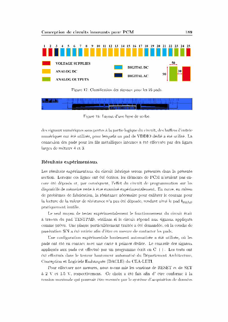
Conception de circuits innovants pour PCM 189
Figure 17: Classication des signaux pour les 25 pads.
Figure 18: Layout d'une ligne de scribe.
des signaux numériques sans pertes à la partie logique du circuit, des buers d'entrée
numériques ont été utilisés, pour lesquels un pad de VDDIO dédié a été utilisé. La
connexion des pads pour les ls métalliques internes a été eectuée par des lignes
larges de métaux 4 et 3.
Résultats expérimentaux
Les résultats expérimentaux du circuit fabriqué seront présentés dans la présente
section. Lorsque ces lignes ont été écrites, les éléments de PCM n'avaient pas en-
core été déposés et, par conséquent, l'eet du circuit de programmation sur les
dispositifs de mémoire reste à être examiné expérimentalement. En outre, en raison
de problèmes de fabrication, la résistance nécessaire pour calibrer le courant pour
la lecture de la valeur de résistance n'a pas été déposée, rendant ainsi le pad IREADpratiquement inutile.
Le seul moyen de tester expérimentalement le fonctionnement du circuit était
à travers du pad TESTPAD, vériant si le circuit répond aux signaux appliqués
comme prévu. Une plaque particulièrement traitée a été demandée, où la couche de
passivation SiN a été retirée an d'être en mesure de contacter les pads.
Une conguration expérimentale hautement automatisée a été utilisée, où les
pads ont été en contact avec une carte à pointes dédiée. Le contrôle des signaux
appliqués aux pads est eectué par un programme écrit en C ++. Les tests ont
été eectués dans le testeur hautement automatisé du Département Architecture,
Conception et Logiciels Embarqués (DACLE) du CEA-LETI.
Pour eectuer nos mesures, nous avons mis les tensions de RESET et de SET
à 2 V et 1.5 V, respectivement. Ce choix a été fait an d' être conforme à la
tension maximale qui pourrait être mesurée par le système d'acquisition de données
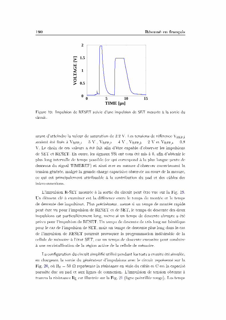
190 Résumé en français
0 0.5 1 1.5
VO
LTA
GE
[V]
TIME [µs]
0
0.5
1
1.5
2
5 10 150
Figure 19: Impulsion de RESET suivie d'une impulsion de SET mesurée à la sortie du
circuit.
avant d'atteindre la valeur de saturation de 2.2 V. Les tensions de référence VREF,i
avaient été xés à VREF,1 = 5 V , VREF,2 = 4 V , VREF,3 = 2 V et VREF,4 = 0.8
V. Le choix de ces valeurs a été fait an d'être capable d'observer les impulsions
de SET et RESET. En outre, les signaux SSi ont tous été mis à 0, an d'obtenir le
plus long intervalle de temps possible (ce qui correspond à la plus longue pente de
descente du signal TIMEREF) et ainsi être en mesure d'observer correctement la
tension générée, malgré la grande charge capacitive observée au cours de la mesure,
ce qui est principalement attribuable à la contribution du pad et des câbles des
interconnexions.
L'impulsion R-SET mesurée à la sortie du circuit peut être vue sur la Fig. 19.
Un élément clé à examiner est la diérence entre le temps de montée et le temps
de descente des impulsions. Plus précisément, même si un temps de montée rapide
peut être vu pour l'impulsion de RESET et de SET, le temps de descente des deux
impulsions est particulièrement long, même si un temps de descente abrupte a été
prévu pour l'impulsion de RESET. Un temps de descente de très long est bénéque
pour le cas de l'impulsion de SET, mais un temps de descente plus long dans le cas
de l'impulsion de RESET pourrait provoquer la programmation indésirable de la
cellule de mémoire à l'état SET, car un temps de descente excessive peut conduire
à une recristallisation de la région active de la cellule de mémoire.
La conguration du circuit simplié utilisé pendant les tests a ensuite été simulée,
en chargeant la sortie du générateur d'impulsions avec le circuit représenté sur la
Fig. 20, où RS = 50 Ω représente la résistance en série du câble et C est la capacité
parasite due au pad et aux lignes de connexion. L'impulsion de tension obtenue à
travers la résistance RL est illustrée sur la Fig. 21 (ligne pointillée rouge). Les temps
Conception de circuits innovants pour PCM 191
C RL
Rs
TESTPAD
Figure 20: Schéma utilisé pour la simula-
tion de la charge à la sortie du générateur
d'impulsions au cours de la caractérisation
expérimentale.V
OLT
AG
E [V
]
TIME [µs]
0
0.5
1
1.5
2
2 3 80
. . .
1 4 5 6 7
MeasuredC = 200 pF
Figure 21: Front montant et descendant de
l'impulsion de RESET (mesuré et simulé).
de montée et descente simulés sont en excellent accord avec ces mesurés, qui sont
également présentées dans la gure (ligne bleue) à des ns de comparaison.
La présence de l'énorme charge capacitive ci-dessus ne permet pas d'apprécier
pleinement le contrôle de la pente de descente de l'impulsion de SET à l'aide de
signaux SSi (Fig. 22). Bien que l'eet de ces signaux de contrôle soit évident quand
un long temps de descente est désiré, ceci n'est pas le cas quand une plus vite
descente de l'impulsion est désirée, et les impulsions générées ont des pentes de
descente qui sont sensiblement superposées.
La Fig. 23 montre les impulsions de RESET générées lorsque la tension VREF,
est xée à 5 V et la tension VREF,2 diminue à partir de 5 V jusqu'à 0 V, donnant lieu
VO
LTA
GE
[V]
TIME [µs]
0
0.5
1
1.5
1.510 0.5 2
Figure 22: Bords descendant de l'impulsion de SET pour diérentes valeurs de signaux
numériques SSi.
192 Résumé en français
2 3 4 5 6
VO
LTA
GE
[V]
TIME [µs]
0
0.5
1
1.5
2
1 3 40 2
(a)
VO
LTA
GE
[V]
TIME [µs]
0
0.5
1
1.5
2
1 3 40 2
(b)
2 3 4 5 6 7 8
VO
LTA
GE
[V]
TIME [µs]
0
0.5
1
1.5
2
1 3 40 2 5 6
(c)
VO
LTA
GE
[V]
TIME [µs]
0
0.5
1
1.5
2
640 2 8 10
(d)
Figure 23: Impulsions de RESET mesurées, générées avec une tension de référence VREF,1constante et une tension VREF,2 variée.
à des valeurs croissantes de durée d'impulsion. Les Fig. 23(a) à 23(d) correspondent
aux diérentes pentes du signal TIMEREF (Fig. 23(a): la pente la plus rapide;
Fig. 23(d): la pente la plus lente) et, par conséquent, à l'échelle de temps diérent
de l'impulsion R-SET. En plus de démontrer qu'il est en eet possible de modier la
durée des impulsions générées par le tensions de référence externes, l'ensemble des
gures ci-dessus donne des informations sur l'échelle de temps obtenue lorsque des
signaux diérents TIMEREF sont générés en interne.
Les Fig. 24 et 25 démontrent la capacité du circuit de contrôler l'amplitude
de les impulsions de RESET et de SET, respectivement, par des tensions externes
VRESET et VSET. Dans les deux cas, la même pente de descente est maintenue.
Il est intéressant de souligner que, dans le cas de l'impulsion de SET, la pente de
descente maintient sa linéarité jusqu'à quelques centaines de mV.
Le générateur d'impulsions proposé est donc capable de générer des impulsions
de RESET et de SET avec une amplitude et une durée qui peuvent être contrôles
par des tensions externes.
Conclusions et perspectives 193
VO
LTA
GE
[V]
TIME [µs]
0
0.5
1
1.5
2
640 2 8
Figure 24: Impulsions de RESET
d'amplitude variée mesurées.
2 4 6 8 10 12
VO
LTA
GE
[V]
TIME [µs]
0
0.5
1
1.5
2
640 2 8 10
Figure 25: Impulsions de SET d'amplitude
variée mesurées.
En conclusion, même si les résultats sur les performances de mémoire ne peuvent
pas être observés, l'activité globale de la conception est avéré être réussie: à partir
de l'étude électrique des dispositifs de mémoire, nous avons spécié la procédure
de programmation adaptée aux matériaux innovants sur lesquelles sont basées ces
cellules de mémoire avancées. Une fois le cahier des charges pour la technique de
programmation désirée a été explicitement indiqué, des schémas de circuits ont été
élaborés et des simulations au niveau du schéma ont été eectuées. Lorsque le
comportement souhaité a été obtenu, le layout physique du circuit a été fait: des
simulations post-layout puis ont servi comme preuve que le circuit était pleinement
opérationnel. Enn, le circuit fabriqué a été caractérisé avec succès, démontrant
ainsi une conception de circuit complète, orant une plateforme de caractérisation
complète pour les tests de dispositifs de mémoire PCM.
Conclusions et perspectives
Parmi les technologies de mémoire non volatile émergentes, la mémoire a change-
ment de phase est le candidat le plus prometteur pour remplacer la mémoire Flash
conventionnelle, orant une grande variété de fonctionnalités, qui en font un excel-
lent candidat pour des applications adaptées non seulement pour les dispositifs de
mémoire embarqués, mais aussi pour les systèmes informatiques haute performance.
L'un des matériaux les plus classiques utilisés dans les applications de PCM est
le Ge2Sb2Te5 (GST), qui est capable d'amener une transition rapide entre le l'état
SET et l'état RESET. Toutefois, la faible température de cristallisation du GST se
traduit par une mauvaise stabilité thermique et, par conséquent, par une rétention
des données limitée. Un autre inconvénient de ce matériau est le courant RESET
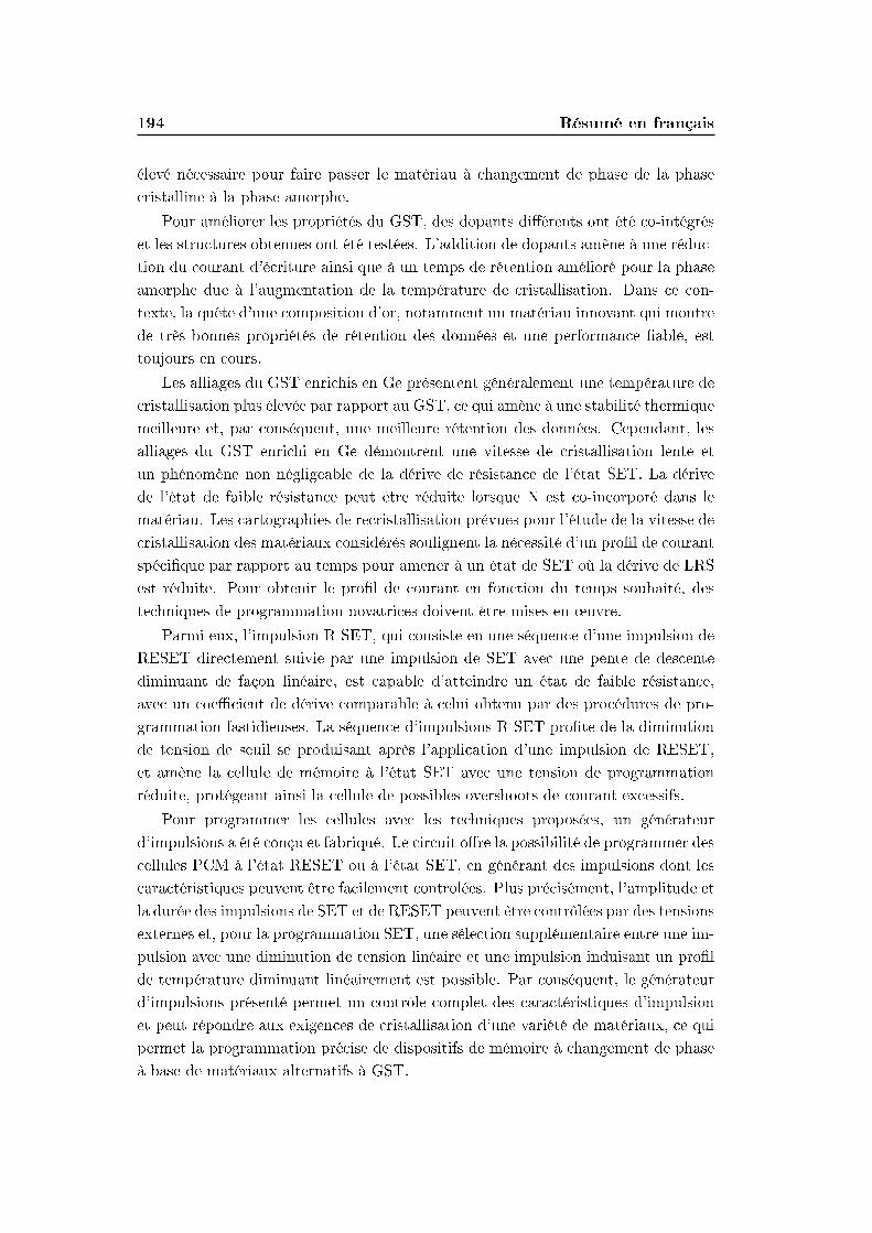
194 Résumé en français
élevé nécessaire pour faire passer le matériau à changement de phase de la phase
cristalline à la phase amorphe.
Pour améliorer les propriétés du GST, des dopants diérents ont été co-intégrés
et les structures obtenues ont été testées. L'addition de dopants amène à une réduc-
tion du courant d'écriture ainsi que à un temps de rétention amélioré pour la phase
amorphe due à l'augmentation de la température de cristallisation. Dans ce con-
texte, la quête d'une composition d'or, notamment un matériau innovant qui montre
de très bonnes propriétés de rétention des données et une performance able, est
toujours en cours.
Les alliages du GST enrichis en Ge présentent généralement une température de
cristallisation plus élevée par rapport au GST, ce qui amène à une stabilité thermique
meilleure et, par conséquent, une meilleure rétention des données. Cependant, les
alliages du GST enrichi en Ge démontrent une vitesse de cristallisation lente et
un phénomène non négligeable de la dérive de résistance de l'état SET. La dérive
de l'état de faible résistance peut être réduite lorsque N est co-incorporé dans le
matériau. Les cartographies de recristallisation prévues pour l'étude de la vitesse de
cristallisation des matériaux considérés soulignent la nécessité d'un prol de courant
spécique par rapport au temps pour amener à un état de SET où la dérive de LRS
est réduite. Pour obtenir le prol de courant en fonction du temps souhaité, des
techniques de programmation novatrices doivent être mises en ÷uvre.
Parmi eux, l'impulsion R-SET, qui consiste en une séquence d'une impulsion de
RESET directement suivie par une impulsion de SET avec une pente de descente
diminuant de façon linéaire, est capable d'atteindre un état de faible résistance,
avec un coecient de dérive comparable à celui obtenu par des procédures de pro-
grammation fastidieuses. La séquence d'impulsions R-SET prote de la diminution
de tension de seuil se produisant après l'application d'une impulsion de RESET,
et amène la cellule de mémoire à l'état SET avec une tension de programmation
réduite, protégeant ainsi la cellule de possibles overshoots de courant excessifs.
Pour programmer les cellules avec les techniques proposées, un générateur
d'impulsions a été conçu et fabriqué. Le circuit ore la possibilité de programmer des
cellules PCM à l'état RESET ou à l'état SET, en générant des impulsions dont les
caractéristiques peuvent être facilement contrôlées. Plus précisément, l'amplitude et
la durée des impulsions de SET et de RESET peuvent être contrôlées par des tensions
externes et, pour la programmation SET, une sélection supplémentaire entre une im-
pulsion avec une diminution de tension linéaire et une impulsion induisant un prol
de température diminuant linéairement est possible. Par conséquent, le générateur
d'impulsions présenté permet un contrôle complet des caractéristiques d'impulsion
et peut répondre aux exigences de cristallisation d'une variété de matériaux, ce qui
permet la programmation précise de dispositifs de mémoire à changement de phase
à base de matériaux alternatifs à GST.
Conclusions et perspectives 195
Même si les performances de PCM semblent être optimisées grâce au dopage à N
du GST riche en Ge, la recherche pour un matériau qui ore le meilleur compromis
entre la rétention des données et la performance de l'état SET est toujours en cours.
Le mécanisme de cristallisation particulier résultant dans la dérive de la résistance
de l'état SET a récemment été compris et l'alliage à changement de phase, avec
une st÷chiométrie optimisée représente un excellent candidat pour le stockage aux
cellules multi-niveaux.
Une fois les mécanismes à l'origine du phénomène de dérive résiduel dans les états
de résistance intermédiaires sont bien compris, la abilité du stockage aux cellules
multiniveaux sera améliorée et le matériau candidat sera en mesure d'orir des états
de résistance intermédiaires dont le contenu n'évolue pas au cours du temps.
Un autre développement intéressant de la technologie PCM sera l'étude du
comportement de la mémoire lorsque l'architecture de la cellule est modiée. Les
mesures eectuées dans le cadre de cette thèse ont été réalisés sur des dispositifs
1R. L'intégration de matériaux innovants à changement de phase dans plusieurs ar-
chitectures de cellules avancées, telles que l'architecture connée, est dicile, mais
les avantages provenant de cette approche, comme le bon connement thermique
du volume actif et l'augmentation de l'ecacité de puissance conséquente, seront
évidents dans le produit nal.
L'une des perspectives les plus importantes concernant ce travail est l'étude
de la programmation par le circuit fabriqué et ses eets sur les performances de
la mémoire. Plus précisément, bien qu'il soit été possible d'analyser les eets de
l'impulsion de R-SET sur les cellules PCM grâce à l'équipement de caractérisation
électrique qui nous a permis de générer cette séquence d'impulsions, les résultats
de l'application des autres techniques de programmation sur les cellules de mémoire
co-integrées doivent encore être étudiés expérimentalement. Lorsque l'optimisation
du fonctionnement du circuit et des performances sont assurées, le circuit peut être
développé pour être utilisé dans une matrice de cellules de mémoire à changement
de phase, aussi visant à explorer des solutions diciles, comme la matrice mémoire
cross-point.
En conclusion, il est un fait indéniable que PCM a commencé à être considérée
comme un véritable concurrent dans le marché des mémoires non volatiles. Étant
compatible avec les procédés CMOS standards et démontrant un ensemble de perfor-
mances remarquable, PCM a suscité l'intérêt de nombreux concurrents industriels
et est désormais une référence pour d'autres technologies de mémoire. Nous croyons
que dans le proche avenir, grâce aussi à des travaux présentés dans cette thèse, les
capacités uniques de PCM seront exploitées dans diérents systèmes électroniques,
allant des applications embarquées à plates-formes informatiques à grande échelle.