Embed Size (px)
Citation preview
IEEE JOURNAL OF SOLID-STATE CIRCUITS, VOL. 29, NO. 3, MARCH 1994 239
Characterization, Modeli:ng, and Minimization ofTransient Threshold Vdti~ge Shifts h MOSFET’s
Theodore L. Tewksbury, III, Member, IEEE, and Hae-Seung Lee, Senior Member, IEEE
Abstract— MOSFET’S subjected to large-signal gate+ourcevoltage pulses on microsecond to millisecond time scales exhibittransient threshold voltage shifts which relax over considerablylonger periods of time. This problem is important in high-accuracy analog circuits where it can cause errors at the 12 b leveland above. In thk paper, transient threshold voltage shifts arecharacterized with respect to their dependence on stress tampli-tude and duration, relaxation time, gate bias, substrate bias, drainvoltage, temperature, and channel width and length. In camtrastto previous studies, threshold voltage shifts are measured ak timeand voltage scales relevant to analog circuits, and are shownto occur even when the effects of Fowler–Nordheim tunneling,avalanche injection, hot carriers, trap generation, self-htating,mobile ions, and dipolar polarizations are absent. A new modelis proposed in which channel charge carriers tunnel to and fromnear-interface oxide traps by one of three parallel pathways.Transitions may occur elastically, by direct tunneling between thesilicon band edges and an oxide trap, or inelastically, by tunnelingin conjunction with a thermal transition in the insulator or at theSi-SiOz interface. Simulations based on this model show excellentagreement with experimental results. The threshold voltage shiftsare also shown to be correlated with l/f noise, in corrobawationof the tunneling model. Techniques for the minimization andmodeling of errors in circuits are presented.
I. INTRODUCTION
IN MOS analog circuits such as switched-capacitor filters
[11, [2], digital-to-analog (D/A), and analog-to-digital (A/D)converters [3], [4], the differential input stages of comparatorsand operational amplifiers are routinely subjected to mo-
mentary asymmetrical voltage stresses during the course oftheir normal operation. In comparators, the magnitude (of thisstress can be as large as half the full scale voltage of theA/D converter, while in operational amplifiers, it can be onthe order of the supply voltage under slewing conditions.MOSFET’s subjected to these large-signal stress conditionsexhibit transient threshold voltage shifts with amplitudes up to1 mV and relaxation times comparable to, or longer than, clockperiods in typical analog circuits [5], [6], causing linearityerrors, long-settling tails, and hysteresis effects. In a previousstudy [5], we measured transient threshold voltage shifts inMOS differential pairs, but the range of bias conditions was
limited and a complete theoretical explanation has not yet
Manuscript received June 30, 1993; revised October 19, 1993. This workwas supported in part by the Semiconductor Research Corporation (SRC)under Contract 92-SP-309 and by the National Science Foundation (NSF)under Contract M1P8858020.
T. L. Tewksbury, III is with Analog Devices Semiconductor, Wllrnington,MA 01887.
H.-S. Lee is with the Department of Electrical Engineering, MassachusettsInstitute of Technology, Cambridge, MA 02139.
IEEE Log Number 9214797.
been offered. This paper extends our previous work to includemeasurements of transient threshold voltage shifts over a widerange of conditions relevant to analog circuits, and presents anew model to explain the results.
Threshold voltage shifts in MOS transistors have beenstudied extensively, particularly in relation to device lifetime
and reliability. However, most of these studies [7]–[9] havefocused on long time scales and high voltages, far outside therange of interest for analog circuits. Under these conditions,
shifts in device characteristics can be caused by a variety
of mechanisms, including the drift of mobile ions [10], thepolarization of molecular dipoles [8], [10], self-heating [111,and charge trapping by interface states and oxide traps [91,
[12]. Under high vertical fields ( > 7 MV/cm), traps canbe created in the insulator [13] and can be charged byFowler-Nordheim tunneling [14] or avalanche injection [15]
of carriers into the oxide bands. At high drain voltages, channelhot carriers can generate interface states [16] and can be in-
jected into the oxide, causing threshold voltage instabilities andrelaxation effects [17], [18]. At the lower voltages and shortertime scales characteristic of normal circuit operation, channelcharge carriers can be exchanged with oxide traps by directtunneling through the interface potential barrier [12], [19].While this mechanism is known to be associated with the l/~noise in MOS devices [20], its manifestation under large-signal
stress conditions has not yet been adequately investigated.This paper reports on a new measurement technique which
isolates direct tunneling from competing effects and enables
this mechanism to be characterized under large-signal stressconditions.
Existing theoretical models of charge trapping by direct tun-nel exchange with oxide traps [7], [9], [19]–[21] are inadequate
to explain the observed threshold voltage transients due toseveral deficiencies. First, many of the assumptions on whichthese models are based are violated under large-signal stress.For example, band bending in the oxide is normally neglectedand Boltzmann statistics are assumed, even though the Fermilevel is driven well into the silicon bands. Second, despitethe fact that it is an elastic process, tunneling is commonly
assumed to occur between the silicon bands and oxide trapsat arbitrary energies within the bandgap, without a plausibleexplanation for how the required change in energy takesplace [22]. Third, we have observed deviations from the strictlogarithmic time dependence derived by previous researchers
[71, [23], and the voltage and temperature dependence of ourmeasurements cannot be explained by existing models. Newtheory is presented here which overcomes these problems and
001 8–9200/94$04,000 1994 IEEE
240 IEEE JOURNAL OF SOLID-STATE.CIRCUITS, VOL. 29, NO. 3, MARCH 1994
enables transient threshold voltage shifts to be quantitativelyexplained and modeled.
Section II begins with a description of the measurementtechnique and presents the key experimental observationswhich suggest a tunneling mechanism. Section III thenpresents a physically based model which is consistent withthe inherently elastic nature of tunneling and includes bandbending in the oxide, Fermi-Dirac statistics, nonuniformtrap densities in energy and space, and correlated mobilityfluctuations. An approximate solution for the thresholdvoltage shift is derived, and the well-known logarithmic timedependence is shown to be a limiting case of a more generalrelation. In Section IV, transient threshold voltage shifts are
characterized and simulated as a function of stress amplitudeand duration, relaxation time, gate bias, substrate bias, drainvoltage, temperature, and device size. Finally, Section Vdiscusses scaling issues, differences between NMOS andPMOS transistors, the relationship between threshold voltageshifts and l/~ noise, and techniques for the minimization andmodeling of errors in circuits,
II. EXPERIMENTAL PROCEDURE
A. Measurement Circuit
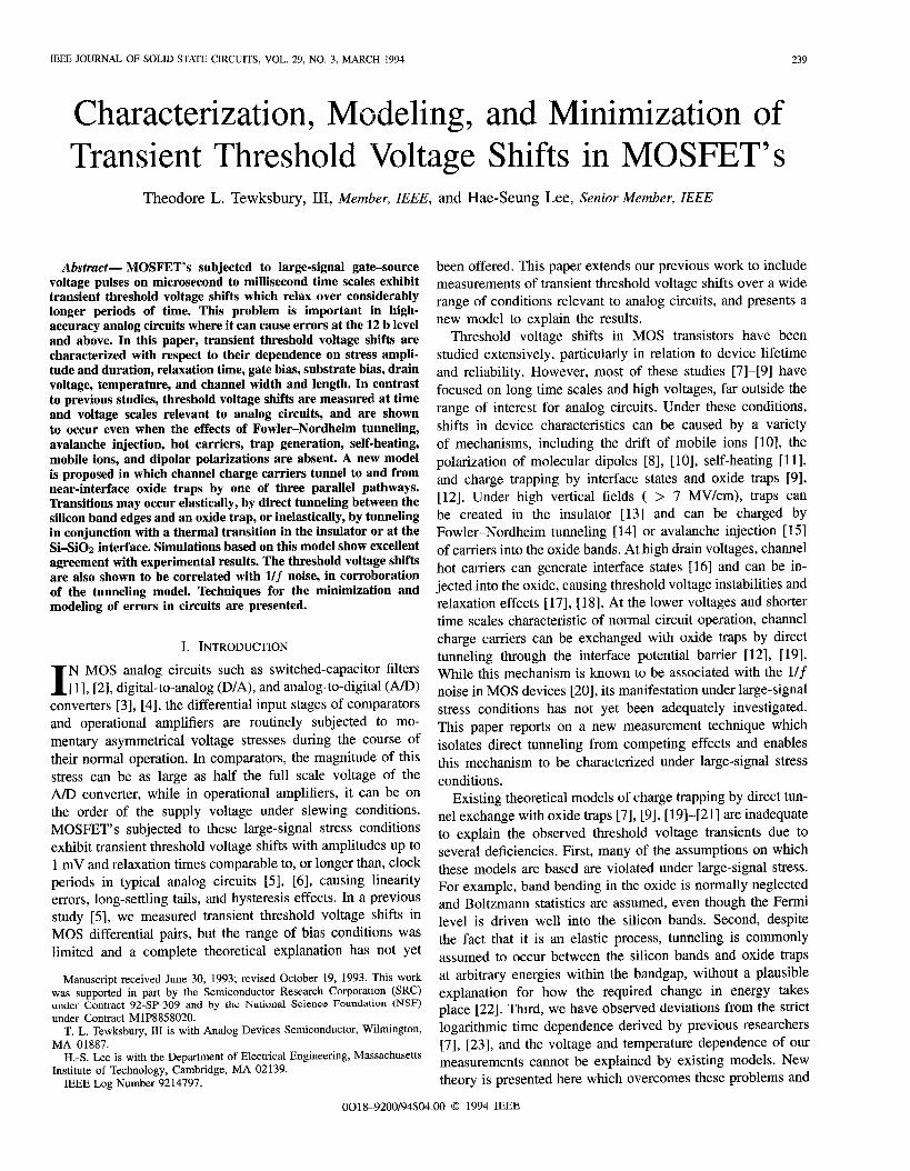
Matched pairs of integrated circuit MOSFET’s were pack-aged and tested using the circuit of Fig. 1(a). Before and afterstress, with the CMOS switches in the positions shown (g$lhigh, @z low), the source-coupled pair comprises the inputstage of a noninverting feedback amplifier with gain (R1 +R2)/R2 x 100 from the gate of the device under test (lkfl)
to the output. A precision voltage supply in the sources setsthe initial gate–source bias, VG,S = –VBIAs. Offset voltage isnulled by adjustment of resistors R3 and R4 so that the gate ofMl is initially at ground. During stress (~1 low, #z high), the
gate of Ml is switched to a voltage source Vp and the opamp isdisconnected from the feedback loop. This prevents stressingof the opamp input stage which could interfere with themeasurement due to thermal or charge-trapping hysteresis [5].Following stress for a period 1 ps < t.<10 ms, the switchesare returned to their original positions. Feedback returns thedrain current of Ml to its initial value by producing anequivalent gate–source voltage shzjit that precisely compensatesfor any change in threshold voltage or mobility resulting fromstress. The amplified gate–source voltage transient is averagedand observed at the output VOU~on a digitizing oscilloscope.The design ensures that the output remains within severalmillivolts of ground at all times during the measurement inorder to prevent overdriving of the oscilloscope preamplifier,which could otherwise contribute long-settling componentsto the response. The output is Schottky-clamped in order toenforce this condition, even under transient conditions.
MOSFET’S are biased in the linear region at lowdrain–source voltage ( IVDS I < 500 mV) so that channelhot carrier generation is negligible. Vertical electric fields aremaintained less than 1.5 MV/cm to prevent trap generation andinjection of carriers into the oxide bands. In order to eliminateself-heating, the device is biased such that no change in power
--R3 R4 @2
1OOcl 100Qlkf2 lkQ $1
I.C TestChip ~
:-------........ .......1
rv’’~:”
%;M2MI~
~,,,,,,, DUT ~ $2.............?
+
(a)
time”
hI
+~~
ts tr time
(b)
Fig. 1. Measurement circuit. (a) Schematic. (b) Clock signals for CMOSswitches.
dissipation occurs during the measurement sequence:
ID,sIVDsl = IDs2VDs2 = ID,s3VDs3 = constant (1)
where the subscripts 1, 2, and 3 indicate the bias points of illl
before, during, and after stress, respectively.
B. Device Fabrication
Threshold voltage shifts were characterized on transis-tors from five different CMOS and BiCMOS processes with250–750 ~ thermally grown SiO z gate dielectrics, as summa-rized in Table I. Samples 1–3 are n-well BiCMOS processesemploying a wet–dry-wet gate oxidation and a blanket boronthreshold voltage adjustment implant. Sample 4 is a p-wellCMOS process with no threshold implant and a dry gateoxidation followed by N2 anneal. Process 5 is a twin-wellCMOS technology with separate n and p threshold implantsand a dry gate oxidation followed by a N2 anneal.
C. Basic Observations
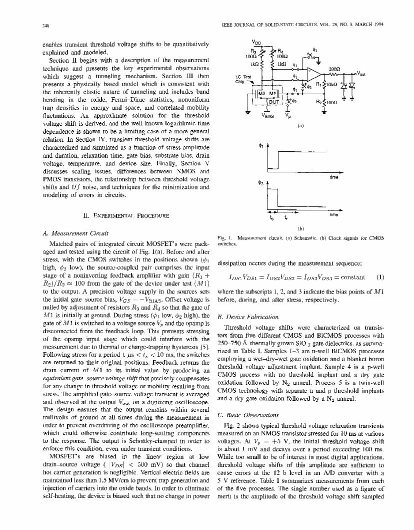
Fig. 2 shows typical threshold voltage relaxation transientsmeasured on an NMOS transistor stressed for 10 ms at variousvoltages. At Vp = +5 V, the initial threshold voltage shiftis about 1 mV and decays over a period exceeding 100 ms.While too small to be of interest in most digital applications,threshold voltage shifts of this amplitude are sufficient tocause errors at the 12 b level in an A/D converter with a5 V reference. Table I summarizes measurements from eachof the five processes. The single number used as a figure ofmerit is the amplitude of the threshold voltage shift sampled
TEWKSBURY AND LEE TRANSIENT THRESHOLD VOLTAGE SHIFTS IN MOSF13T’S 241
TABILE ISTATISTICSOF THRESHOLDVOLTAGESsums INFIVEDIFFERENTPROCESSES(t,= 10 ms, t, = 1 ms)
NMOs AVT (jLv) PMOS A~>(/sV)Process tOX(~) WiL V& \’JJs VP=+5V v, =: –5 v ~Gs Ibs I~=+5v ~<=_5v
(v) (mV) mean u mean 0 — (v) (mV) mean u mean Is1 350 2015 1.0 200 370.0 50.0 –13!5.0 22.4 –1.5 –500 27.2 26.1 –5.3 3.02 350 100/5 1.0 200 700.1 113.5 –368.6 189.1 –1.5 –500 37.3 28.1 –20.0 11.93 750 48/4 1.2 300 482.8 19.4 –135.0 44.6 –2.0 –500 37.2 10.0 –49.6 29.54 500 20/5 1.0 200 65.2 28.0 –338 21.8 –2.0 –500 11.9 2.3 –4,8 1.85 250 20/5 1.2 300 523.6 72.2 –.43’2.8 236.0 –1.4 –500 134.6 93.4 –28.7 17.3
-‘P=5V
4V
3V2V
Iv
-lV-2V NMOSW/L.l 00Lm/5~m-3V Process 2-4V v~~-v~=o,5v V,,3.=0.3V-5V 1~~.150~
10 10.0 100.0
Relaxation Time t, (ins)
Fig. 2. Measured threshold voltage relaxation transients in an NM(M tran-sistor stressed for 10 ms at various voltages.
a fixed delay, t. = 1 ms, after stress for t, = 10 ms. Thepeak threshold voltage shift may be much larger, but (cannotbe measured due to the finite response time of the circuit. Foreach process, the mean threshold voltage shift is calculatedfrom measurements on a randomly chosen sample of 10-20devices from the same lot.
Several observations can be made from these data. 1) Thethreshold voltage shifts cannot be caused by hot carriers,trap generation, self-heating, avalanche, or Fowler–Nordheiminjection since the measurement conditions have been specifi-
cally designed to preclude these effects. 2) The polarity of thethreshold voltage shifts is always in the same direction as thestress voltage, AVT/VP >0, opposite to that which would beproduced by mobile ions or dipolar polarizations [10]. 3) Thelarge inter- and intraprocess variations of the threshold voltageshifts are consistent with a mechanism that depends on arandom distribution of defects. However, the time constants of
the decay are too long to be explained entirely by fast surfacestates at the Si–Si02 interface. These observations, tolgetherwith the nearly logarithmic time dependence of the relaxation,suggest a mechanism in which channel charge carrkrs areexchanged with oxide traps by direct tunneling [7], [23].
III. TUNNELING MODEL
A. Kinetics
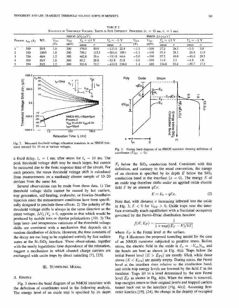
Fig. 3 shows the band diagram of an NMOS transistor withthe definition of coordinates used in the following analysis.The energy level of an oxide trap is specified by its depth
Poly Oxide Silicon
TA
---------o--q&x —
x- mox 0
Fig. 3. Energy band diagram of an NMOS transistor showing definition ofcoordinates (1’Bs = O).
Et below the SiOz conduction band. Consistent with thisdefinition, and contrary to the usual convention, the energyof an ellectron is specified by its depth E below the SiOz
conduction band at the interface (% = O). The energy E ofan oxide trap therefore shifts under an applied oxide electricfield ~ by an amount qt?x:
E = Et – q&x. (2)
Note that, with distance x increasing leftward into the oxidein Fig. 3, ~ < 0 for VG.S > 0. Oxide traps near the inter-face eventually reach equilibrium with a fractional occupancy
governed by the Fermi–Dirac distribution function
f (E, EF) =1
1 + exp[(EF – E)/kT’]
where ~F’ is the Fermi level at the surface.Fig. 4 illustrates the proposed tunneling model for the case
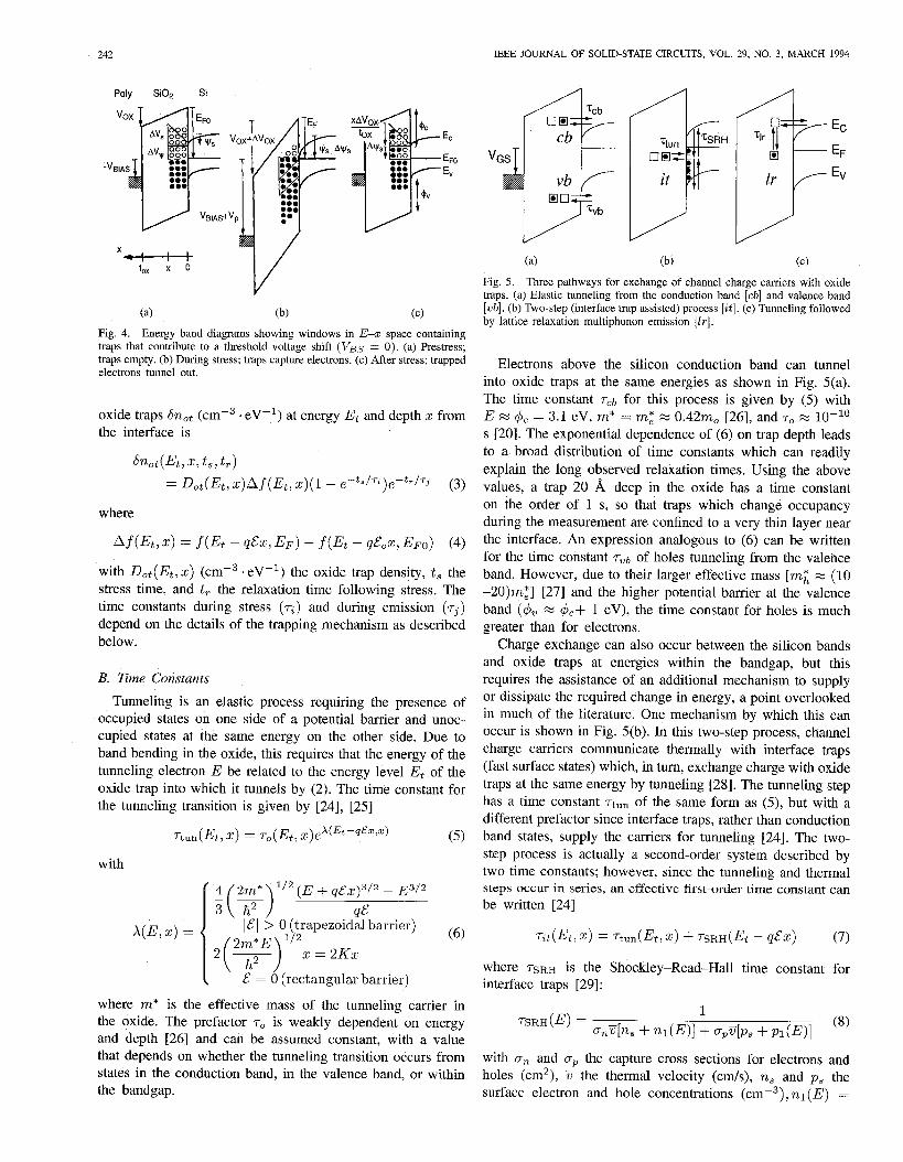
of an NMOS transistor subjected to positive stress. Beforestress, tlhe electric field in the oxide is &O = – VLJtox andthe bands are bent as shown in Fig. 4(a). Traps below theinitial Fermi level (E > EFO ) are mostly filled, while thoseabove (E < EFO) are mostly empty. During stress, the Fermilevel at the interface rises relative to the conduction band,and oxide trap energy levels are lowered by the field & in theinsulator. Traps fill to a level determined by the new Fermilevel EF as shown in Fig. 4(b). When the stress is removed,trap energies return to their original levels and trapped carrierstunnel back out to the interface [Fig. 4(c)]. Assuming first-order kinetics [19], [24], the change in the density of occupied
IEEE JOURNAL OF SOLID-STATE CIRCUITS, VOL. 29, NO, 3, MARCH 1994242
Poly sio~ Si
-“E+“&;o..(a) (b) (c)
Fig. 4. Energy band diagrams showing windows in E–z space containingtraps that contribute to a threshold voltage shift (VBS = O). (a) Prestress;traps empty. (b) During stress; traps capture electrons. (c) After stress; trappedelectrons tunnel out.
oxide traps tint (cm–3 . eV– 1) at energy Et and depth z fromthe interface is
~not(&,~,~,,&)
= DOt(Et, $) Af(Et, z)(1 – e–t’/7’)e–t’/T~ (3)
where
A$(12t, z) = ~(llt – q&z, EF) – f(E, – q&z, 17FO) (4)
with DOt(13t, ~) (cm–3 . eV– 1) the oxide trap density, t. thestress time, and t. the relaxation time following stress. The
time constants during stress (ri) and during emission (-i-j)
depend on the details of the trapping mechanism as described
below.
B. Time Constants
Tunneling is an elastic process requiring the presence ofoccupied states on one side of a potential barrier and unoc-cupied states at the same energy on the other side. Due toband bending in the oxide, this requires that the energy of thetunneling electron E be related to the energy level Et of theoxide trap into which it tunnels by (2), The time constant forthe tunneling transition is given by [24], [25]
with
{
(–)4 2m* 1/2 (E+ qtSx)3/2 – E3/2
i FL2
A(E, X) =I&l >0 (trapezoid~~barrier)
2m”E ‘I’z = 2KZ
()
(6)
2— ~,2
L“ ‘ Z = O (rectangular barrier)
where m* is the effective mass of the tunneling carrier inthe oxide. The prefactor -rO is weakly dependent on energyand depth [26] and can be assumed constant, with a valuethat depends on whether the tunneling transition occurs fromstates in the conduction band, in the valence band, or withinthe bandgap.
47%Cb
❑ n
cbv~~
vb❑ u
‘kb
(a)
?
;-j!.,
il
EC‘qr
El EF
lrEv
/
(b) (c)
Fig. 5. Three pathways for exchange of channel charge carriers with oxidetraps. (a) Elastic tunneling from the conduction band [cb] and vafence band[vb]. (b) Two-step (interface trap assisted) process [it]. (c) Tunneling followedby lattice relaxation multiphonon emission [lr].
Electrons above the silicon conduction band can tunnelinto oxide traps at the same energies as shown in Fig. 5(a).The time constant ‘TCbfor this process is given by (5) withE z qbC= 3.1 eV, m* = m; % 0.42m0 [26], and To x 10–10s [20]. The exponential dependence of (6) on trap depth leads
to a broad distribution of time constants which can readily
explain the long observed relaxation times. Using the abovevalues, a trap 20 ~ deep in the oxide has a time constanton the order of 1 s, so that traps which change occupancyduring the measurement are confined to a very thin layer nearthe interface. An expression analogous to (6) can be writtenfor the time constant rub of holes tunneling from the valeiiceband. However, due to their larger effective mass [m; N (10
–20)m~ ] [27] and the higher potential barrier at the valenceband (4V % q$~+ 1 eV), the time constant for holes is muchgreater than for electrons.
Charge exchange can also occur between the silicon bandsand oxide traps at energies within the bandgap, but thisrequires the assistance of an additional mechanism to supplyor dissipate the required change in energy, a point overlookedin much of the literature. One mechanism by which this canoccur is shown in Fig. 5(b). In this two-step process, channelcharge carriers communicate thermally with interface traps
(fast surface states) which, in turn, exchange charge with oxidetraps at the same energy by tunneling [28]. The tunneling step
has a time constant 7tU= of the same form as (5), but with adifferent prefactor since interface traps, rather than conductionband states, supply the carriers for tunneling [24]. The two-step process is actually a second-order system described bytwo time constants; however, since the tunneling and thermalsteps occur in series, an effective first-order time constant canbe written [24]
Tit(Et,Z) = Tt.n(Et,X) + 7sRH(Et– q~z) (7)
where ~sRH is the Shockley–Read–Hall time constant forinterface traps [29]:
1(8)7SRH(E) = OnU[n, + nl (E)] + OPOS + ~l(E)l
with am and ffp the capture cross sections for electrons andholes (cm2), D the thermal velocity (cm/s), n, and p. thesurface electron and hole concentrations (cm-3), nl (E) =
TEWKSBURY AND LEE: TRANSIENT THRESHOLD VOLTAGE SHIFTS IN MOSFIET’S 243
n, exp(EF – E)/kT, and pl (E) = p. exp(E – Er)/kT.
In strong inversion, the thermal time constant for interfacetraps near the band edges is on the order of 100 ps, ~sothatthe process becomes tunneling-limited (~it w ~tUn). However,
for traps near midgap or at low temperatures, the system canbecome thermally limited (T,t = TSRH ).
An electron can also tunnel elastically into an excited state
of an oxide trap, as shown in Fig 5(c), which subsequently
relaxes to its equilibrium ground state with energy loIss oc-curring by cascade phonon emission [30] or lattice relaxation
multiphonon emission [31]. The time constant for this phonon-assisted process has the same form as (8), but with a capturecross section that decreases exponentially with depth into theoxide [19], [24]. In addition, the capture cross section forthe lattice relaxation process is thermally activated with an
energy barrier EA ranging from 100 to 600 meV [32]. Thecapture cross section in (8) therefore takes the form a(~) =ao exp(–EA//c7’) exp[–~(~,, x)], where A is evaluated atthe conduction band energy E = ~. from which the tunnelingtransition occurs. Assuming equal capture cross sections for
electrons and holes, the time constant for lattice relaxation cantherefore be written as shown in (9) at the bottom of this page.Note that the time constants for both inelastic mechanisms
(7)-(9) are thermally activated through nl and pl, dependinversely on the surface carrier concentrations, and increase
exponentially with the spatial depth of the trap in the oxide.Rigorous deviations of the these time constants from quantummechanics can be found in [24].
C. Effective Threshold Voltage Shft
The device under test is initially biased in the linear regionwith drain current
IDS = p,N~lQnlVDs (lo)
where lQn I = COX(VGs — VT — V~,S/2) is the inversioncharge (C/cm2). By partial differentiation of (10) at constantVD,S, the equivalent gate–source voltage shift 6VG.S requiredto restore the drain current to its initial value following stress(81D,s = O) is
W&= w-- - %0x
(11)
The contribution to the threshold voltage shift due to a trappedcharge density 6nOt at energy Et and depth x is [33]
6VT = + ()1 – ~ 6nOt6Et6x.0x 0x
(12)
In addition to shifting the threshold voltage, the capture of acarrier by an oxide trap induces a change in the mobility ofchannel carriers due to increased scattering from the chargedtrap site. Since the mobility perturbation 6K is correlated with
the fluctuation in the number of trapped carriers, it can bewritten [24], [34]
6U = –~~S(x)q6nOt6Et8x N–qp~ S06nOt 6Et 6x
lQnl(13)
where 6’(%) % S~/ lQ~ I is the scattering rate (C/V.s) and SOis a constant with a value of approximately 0.02 V . s/cm2 for
an NMOS transistor [35].
Summarizing these results, traps at energies above theconduction band (cb) or below the valence band (vb) areassumed! to communicate with oxide traps by elastic tunneling,while transitions involving traps at energies between the bandsmust occur either by the interface state assisted (two-step)
process (it) or by the lattice relaxation process (lr). Sincethe bending of the oxide bands shifts trap energy levels withrespect to the interface according to (2), traps which fill by oneof these mechanisms may empty by another. We shall denoteby i/j that component of the threshold voltage shift due totraps which fill by mechanism i during stress and empty bymechanism j following stress, where i, j c {cb, vb, it, lr}.
Substituting (3), (12), and (13) into (11) and integratingthe contributions due to traps at all energies and depths inthe oxidle, the equivalent gate–source voltage shift due tocomponent z/j is
EQ
‘vGs(,/,) (t., t,) = * /’:’ / DOt(Et, z) Af(Et, z)o 0
where EG z 9 eV is the energy gap of Si02 and
(14)
t:x= tox(l + #N&). (15)
The upper limit of integration in (14) has been changed fromtox to t;x on the basis that the integrand is negligible atthis limit due to the exponential dependence of ~i on x.Comparison of the form of (14) with (3) and (12) indicates thatthe equivalent gate–source voltage shift, which is due to bothmobility and threshold voltage fluctuations, can be interpreted
as an efective threshold voltage shift with a scaled oxidethickness given by (15). The total effective threshold voltage
shift is just the superposition of all of these components:
D. Approximate Voltage and Time Dependence
Insight into the voltage and time dependence of (14) canbe obtained by consideration of the important special caseof strong inversion operation at room temperature. In or-der to obtain closed-form solutions, we make the followingassumptions.
1m(-%~) = . —
eEA/~Te~(&,Z).
oov[ns + nl(Et -- @z) +-p. + II1(J%– qt~)](9)
244
1)2)
3)4)
Uniform oxide trapStep approximation
distribution Dot (Et,Z) = Dot.
to the Fermi function:
Negligible mobility fluctuations (Kiv So = O).x << tox since typical tunneling depths are less than 20
~ while 250 ~ s t.. 5750 ~.5) Rectangular tunneling barrier: Using assumption 4), this
approximation results in less than 10% error in average barrierheight for 5 V across a 500 ~ oxide.
6) Pinning of the Fermi level at the conduction band edgeduring positive stress (J!3F % JTc).
7) VBS = o.Under these assumptions, all three processes 5), 7), and 9)
are tunneling-limited with a time constant of the form ~s (x) =~0~ exp(2Kx) during stress and T, (x) = TOTexp(2Kx) duringrelaxation, where the prefactors generally differ due to the biasdependence of (8) and (9). As shown in the Appendix, the totalth~eshold voltage shift can then be writtencomponents:
AVT = Av$ + Av&
where
as the sum of two
(17)
(18)q2DOttOX
Av+ = ~~eox‘“s’” (1+-)
‘AvOxln (’+%)‘Vf = 4K2eOz
“[~+:’n(’+-)+’n(%)l‘1’)As shown in Fig. 4, the components AV4 and AVE correspondto windows in E–x space containing those traps that changeoccupancy during the measurement sequence, thereby con-tributing a nonzero value to the integrand in (14). The su~acepotential component AV4 is due to traps at energies within thesilicon bandgap that change occupancy as a consequence of thechange in Fermi level or, equivalently, the change in surfacepotential A~s = (13Fo – E~)/q that occurs during stress. Ona microscopic level, the traps that comprise this componenttherefore fill and empty via the it/itor lr/lr mechanismsdescribed above. The band-bending component AVE, whichis driven by the change in voltage AVOX = (Eo – S)t..
across the oxide, is due to traps that are lowered belowthe conduction band during stress and raised above it when
the stress is removed. The traps which contribute to this
component therefore fill and empty by the lrlcb andlor itlcb
processes.Equations (18) and (19) show that a pure logarithmic time
dependence, as predicted by previous models [7], [23], resultsonly when band bending in the oxide is neglected (AVOZ = O)and only in the limits ts >> t., both assumptions of whichare violated under typical circuit operating conditions. Fort. >> t,,the inclusion of the band-bending term contributesa component that goes as logz(time) to the usual log(time)dependence, while for t. >> t.,the present theory predictsthat the decay will approach l/tr.
IEEE JOURNAL OF SOLID-STATE CIRCUITS, VOL. 29, NO 3. MARCH 1994
IV. RESULTS
While (18) and (19) describe the general features of the
threshold voltage shifts with voltage and time, the accuratemodeling of their temperature and bias dependence demands
a more exact treatment. In this section, (14) is integratednumerically using the energy-dependent time constants of
(5), (7), and (9), with a trapezoidal potential barrier andFermi-Dirac statistics. All of the parameters in (14) are known
quantities, with the exception of Dot(Et, ~), which is treatedas an adjustable fitting parameter. The trap distribution can bemodeled quite generally by a function of the form
N
DOt(Et, x) = Doe–xl’” + ~ Digt(Et)[l – g,(Et)]e-~/~‘i=l
where
1gi(G) =
1 + exp[(13i – Et)/AEi] “
(20)
Equation (20) is the superposition of a uniform trap densityDo and IV peaks at the energies Et. By varying the numberand the spread AE~ of these peaks, a wide variety of trapenergy distributions can be modeled ranging from uniformto discrete levels. The trap density is assumed to decay with
increasing depth into the oxide with a characteristic length xi.Since only traps within 20 ~ of the interface are of interest,this assumption is not restrictive and simplifies the numericalintegration.
In the following sections, transient threshold voltage shiftsare characterized over a wide range of bias and stress con-
ditions and compared with simulations based on this model.Without loss of generality, an NMOS transistor is assumed.Differences between threshold voltage shifts in NMOS andPMOS transistors are addressed in Section V-B.
A. Stress Voltage
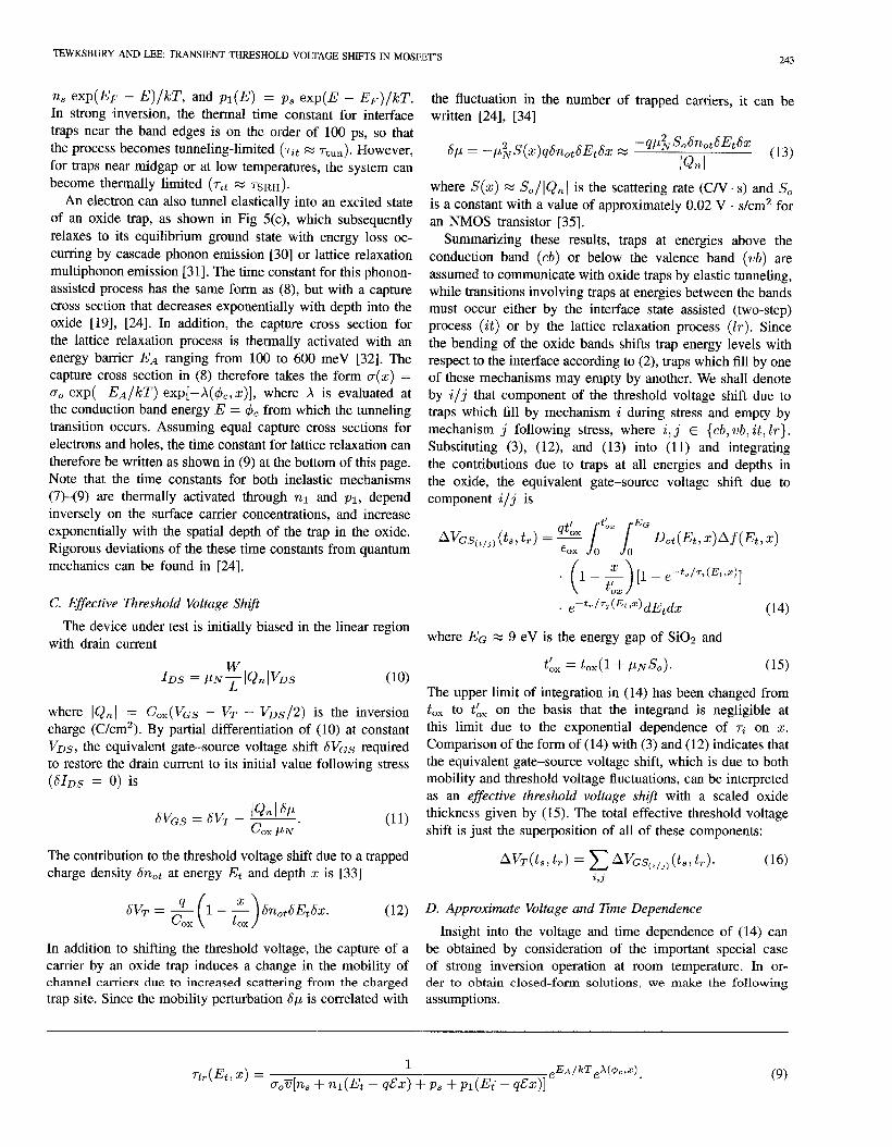
Fig. 6(a) plots the measured threshold voltage shift versus
applied stress voltage for a stress time of 10 ms. Simulations
using the two-step model (7) are also shown. The trap distribu-
tion in (20) was fit to the data with lV = 1 and the parameter
values in Table II. As shown in the inset to Fig. 6(a), this
trap distribution increases with energy above the conduction
band, peaking at about 0.2 eV above the band edge, consistent
with previous findings [34], [36], [37]. Also shown in Table
II are values for the time constant prefactors ~.bo (%0) and
Tcbl (~,tl ) for tunneling to and from conduction band states
(interface traps) during relaxation and stress, respectively. In
Fig. 6(b), the same data are shown, together with simulations
using the lattice relaxation model (9). While the forms of the
extracted trap densities in Fig. 6(a) and (b) are identical, their
magnitudes differ somewhat depending on which model is
used. The voltage dependence can be explained equally well by
either mechanism, making it difficult to experimentally resolve
their relative contributions.
For positive stress, most of the applied voltage is dropped
across the oxide (AV& = VP), and the itlcb and lrlcb
components, which comprise the band-bending term AV,,
TEWKSBURY AND LEE: TRANSIENT THRESHOLD VOLTAGE SHIFTS IN MOSFET’S 245
800~- 2.5
> 2.0
-- ‘!~l
x.onm NMOS (Process 1)s+ 600 - ?Q .2 1Opm/5~m
E 1,5 0.5
>’ 400 -L-::10
Q 2.0 it/cb~ 5.0
200 - :s 0“0-1o_____ >L.:’:”~tilt
8 -0.5 0.0 0.5EC-E (eV)
,.-al ,.- cblcb%’ 0
vblit ., .. .. . .......-= ------ ,.-,----
----------2 vblvb
-600 i 1-lo -5 0 5 10
Stress Voltage Vp (Volts)
(a)
800 ,
0[ L -- . .. . .... ... /
-400}~+Q-’ .F:K.;LationMo(,e,{-&-Jf) ~_.J
-lo -5 0 5 10
Stress Voltage V, (Volts)
(b)
Fig. 6. Measured and simulated dependence of threshold voltage shift onstress voltage. (a) Two-step model. (b) Lattice relaxation model.
TABLE IIPARAMETERVALUESUSEDIN SIMULATIONS(TWO-STEP MODEL)
ModelUnits
ProcessParameter 1 2 5
Do cm ‘3 eV–l 7.0 X 10L6 6.0 X 10¹⁶ 2.5 X 10¹⁶D1 cm– 3 eV–l 2.3 x 10¹⁷ 2.9 X 10¹⁷ 2.5 X 10¹⁷El eV 2.9 3.0 3.1AEI eV 0.1 0.1 0.03Xo A 5.0 5.0 5.0
xl A 20.0 20.0 50.0
TcbO ns 0.1 9.0 0.2
Tcb1 ns 0.1 9.0 1.0
T,to ns 0.1 9.0 8.07i~~ ns 0.1 9.0 1.0
~n, up, ~. cmz 1.0 x 10⁻¹⁵ 1.0 x 10–’5 1.0 x 10⁻¹⁵
increase nearly linearly with voltage, as predicted by (19). The
components it/itand lr/lr follow the voltage dependence of
,AV@ in (18), saturating in strong inversion and accumulation
when the surface potential becomes pinned (A@s x O). Note,however, that the lr/lr component does not completely clamp
NMOS (Process 2)
- W/L=l OOpm/5bm
- VDs=300mV IDS=150~A
vBs=-3v
z .5001~1=
Stress Voltage Vp (VOltS)
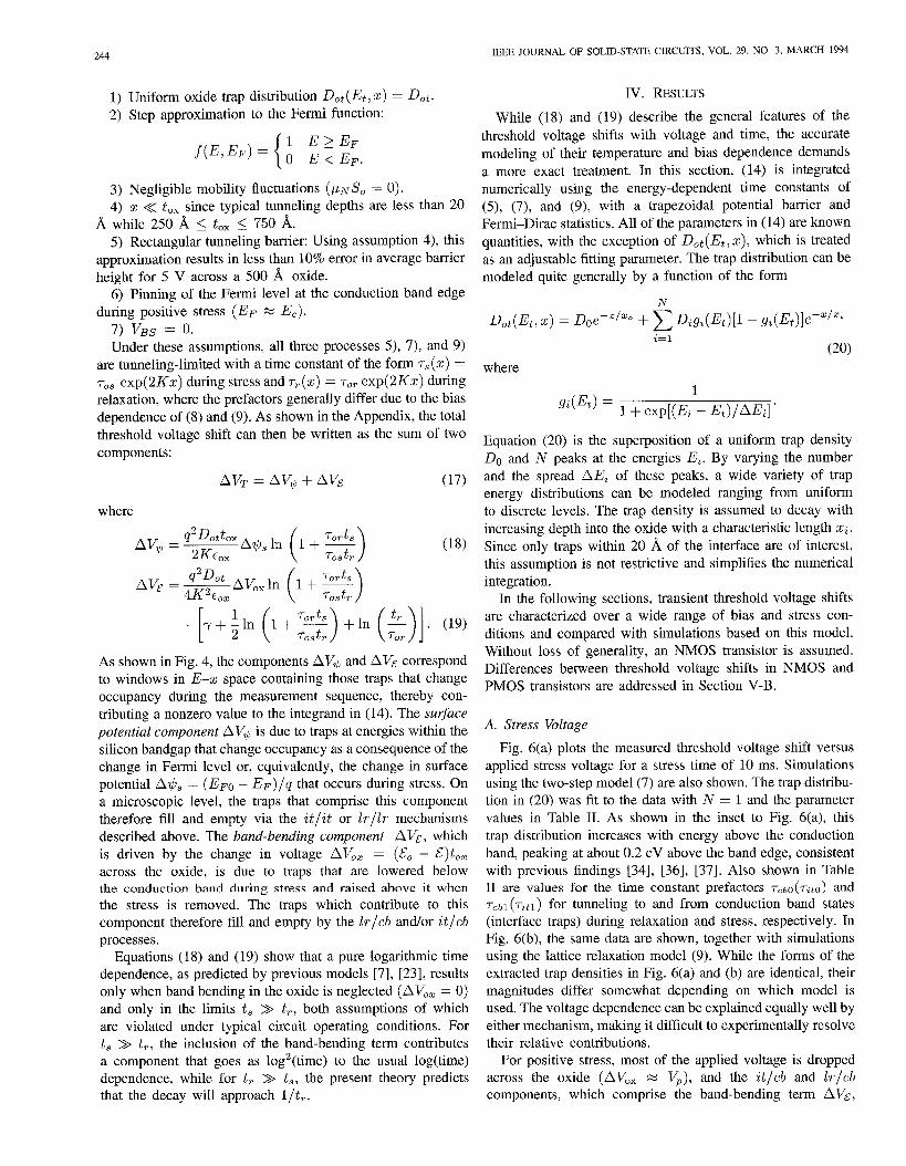
Fig. 7. Threshold voltage shift versus stress voltage with substrate bias asa parameter.
because the prefactor of the time constant in (9) is voltagedependent. In strong inversion, the prefactor decreases with
increasing gate voltage as TO x (Onun.)-l (x [cox(v~~ -VT)] -1. This leads to a slight increase in AVT over thatpredicted from the change in surface potential alone.
For negative stress voltages which pulse the surface intodepletion, the behavior of AVT with voltage is stronglydependent on temperature and stress time. When the stresstime is long compared with the time constants for oxide trapswithin the bandgap (t, >> Tit, rzr ), electron emission canfollow the applied voltage, and the AV@ components zt/it
and ir/lr track the change in surface potential as the Fermilevel sweeps down through the bandgap, as shown in Fig.
6. At shorter stress times or lower temperatures, the timeconstants in (7) and (9) can become too long for traps withinthe bandgap to follow the applied voltage (t, << ‘m,‘n,).
Under these conditions, electrons remain trapped until thesurface accumulates, at which point the time constants becomesufficiently short for emission to occur, producing an abruptnegative threshold voltage shift as shown in Fig. 7.
After accumulation is reached, further increases in themagnitude of VP result in negligible changes in thresholdvoltage shift for two reasons. First, the tunneling probabilityfor holes is much smaller than for electrons, as explainedabove. Second, it is well known that traps above midgaptend to be acceptor-like, while those below are donor-like[38]. The discussion above assumed acceptor-like traps, whichempty and become neutral during negative stress. However,large negative stress voltages drive the Fermi level down to
the valence band edge, causing donor-like traps to emptyand become positively charged. When the surface returnsto inversion, the high electric field ( 106–10s V/cm) createdacross the thin oxide barrier by the dipole layer of positivelycharged dlonor traps and negative inversion layer charge causeselectrons to be recaptured in a period too short to be measuredby the circuit. This high field condition does not occur forpositive stress because occupied acceptor traps and inversionlayer electrons have the same polarity.
B. Substrate Bias
Fig. 7 shows the effect of a substrate-source voltage VBson the AVT – VP characteristics. As VB,S was varied, the initial
246
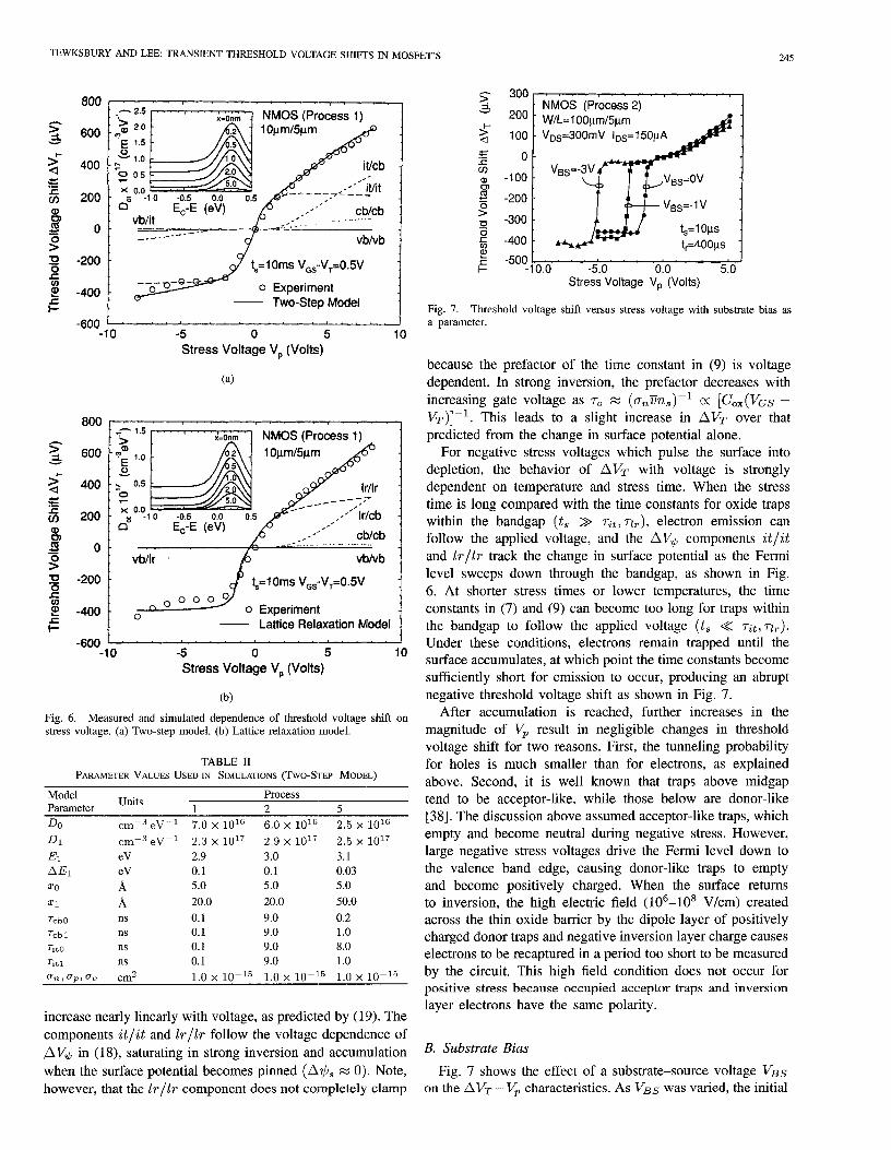
1500s~ NMOS (Process 2) W/L=500Lm/5pm
v@3-v~=o.5v v~5.=o.3v
4gsm 500 - ■
%. Experiment (VP= -5V)
g o■ Experiment (Vp = +5v) .
s — Simulation~
J? -500 -ma2* -1000 .,5
1.0 1.5 2.0 2.5 3.0
initial Gate-Source Bias VGs (V)
Fig. 8. Dependence of threshold voltage shift on prestress gate–sourcevoltage bias.
gate–source bias was adjusted to compensate for the back-gateeffect, maintaining the prestress value of the drain current at aconstant level. The characteristics therefore change negligiblyin the positive direction because the relationship between
the electron quasi-Fermi level and the conduction band edgeis fixed. However, since the application of a substrate bias
VBS shifts the point at which accumulation occurs to a morenegative voltage, the steps in the characteristics shift alongthe VP axis by an amount [24]
where @. is the surface potential in strong inversion and~ = Jm/COX is the back-gate effect parameter. The
first term in (21) accounts for the splitting of the electron andhole quasi-Fermi levels at the interface by the applied substratebias. The second term is just the voltage required to cancel theincrease in gate–source bias which was applied to compensatefor the back-gate effect.
C. Initial Gate–Source Bias
Previously, it had been reported that the threshold
voltage shifts produced in NMOS transistors under positivegate–source voltage stress decrease with increasing draincurrent [5]. This observation can now be explained by thetunneling model. Assuming that the Fermi level becomespinned at the conduction and valence band edges in stronginversion and accumulation, respectively, the maximumamplitude of the surface potential component AV@ is
proportional to Ill. – 13FoI for positive and to IJ!3F0– 13UIfor negative stress. As the initial level of inversion increaseswith increasing gate bias, 17Fo moves closer to E. and fartherfrom Ev. This causes the magnitude of the threshold voltageshift to decrease for positive and increase for negative stress,as shown in Fig. 8.
D. Drain–Source Voltage
While measurements at low drain voltages enable the tun-neling mechanism to be isolated from competing effects,MOSFET’s in analog circuits are normally biased in saturationwhere the transconductance and output resistance are high. Atarbitrary drain biases, (1) no longer holds, and a change in
IEEE JOURNAL OF SOLID-STATE CIRCUITS, VOL. 29, NO. 3, MARCH 1994
s 1000~ NMOS (Process 2)
>+ W1l-=100Lm/5~mdc “.._o*O.n.O**-o-*o*
)
.-_cm
~ 500g
$ VG~-VT=0.8Vg VP.5VE(n t~=l Oms tr=l msg
f OO.O 2,0 4.0 6,0 8.0 10.0Initial Drain Voltage VD~ (V)
tlg. 9. Drain bias dependence.
/
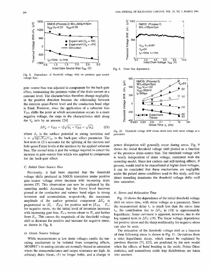
NMOS (Process 5)W/L=20pm/5pm vp=5\
v~~-vl=l .OvVDs=300mV A 3V
e
tr=500~so lV
~Ao*&;. .
~ -400 I0.0001 0.001 0.01 0.1 10
Stress Time t, (k)
Fig. 10. Threshold voltage shift versus stress time with stress voltage as aparameter.
power dissipation will generally occur during stress. Fig. 9shows the initial threshold voltage shift plotted as a functionof the prestress drain–source bias. The threshold voltage shiftis nearly independent of drain voltage, consistent with thetunneling model. Since hot carriers and self-heating effects, ifpresent, would tend to be exacerbated at higher drain voltages,it can be concluded that these mechanisms are negligible
under the pulsed stress conditions used in this study, and thatdirect tunneling dominates the threshold voltage shifts wellinto saturation.
E. Stress and Relaxation Time
Fig. 10 shows the dependence of the initial threshold voltage
shift on stress time, with stress voltage as a parameter. Since
the measurement delay tr is much less than the stress time
t.,the contribution due to AVO in (18) is approximatelylogarithmic. Some curvature is apparent, however, due to thelog squared term in AVS (19). The linear voltage dependencefor positive stress and the sharp nonlinearity for negative stresscan also be seen.
The relaxation of the threshold voltage shift as a functionof time following stress is shown in Fig. 11. Deviations froma strict logarithmic decay, which cannot be explained byprevious theories [7], [23], are predicted by the new modelwhen the effects of band bending in the oxide, Femi–Diracstatistics, and nonuniform oxide trap distributions are takeninto account.
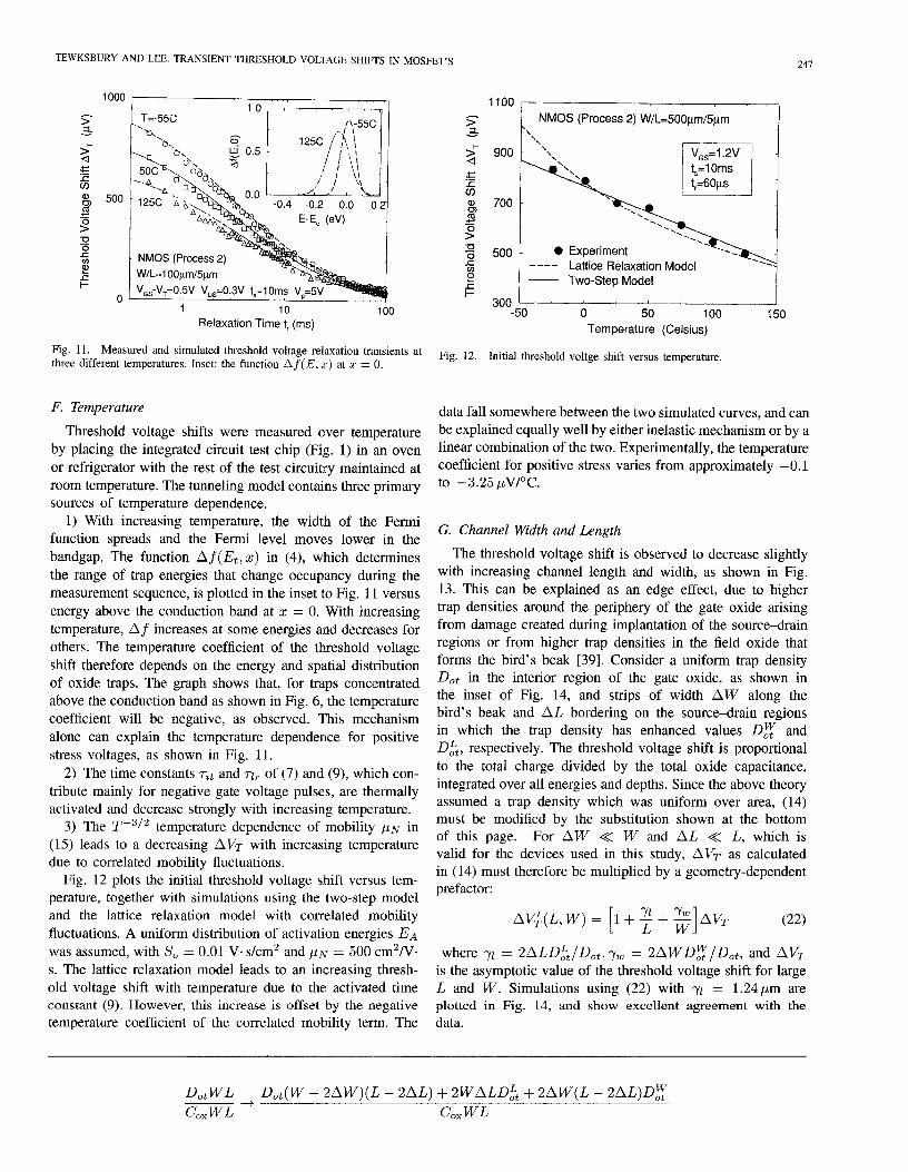
TEWKSBURY AND LEE. TRANSIENT THRESHOLD VOLTAGE SHIFTS IN MOSFET’S247
100010
T=-55C
‘m.‘o, q
50C
-0.4 -0,2 0.0 0 T
NMOS (Process 2)
W/L.l 00ym/5pm
VG~-VT=0,5V VD~=0.3V t,=l Oms V,=5Vo
1 10 1{Do
Relaxation Time t, (ins)
Fig. 11. Measured and simulated threshold voltage relaxation transients atthree different temperatures. Inset: the function Af(13, Z) at r = O.
F. Temperature
Threshold voltage shifts were measured over temperature
by placing the integrated circuit test chip (Fig. 1) in an oven
or refrigerator with the rest of the test circuit~ maintained atroom temperature. The tunneling model contains three primarysources of temperature dependence.
1) With increasing temperature, the width of the Fermifunction spreads and the Fermi level moves lower in the
bandgap. The function A~(13t, z) in (4), which determines
the range of trap energies that change occupancy during themeasurement sequence, is plotted in the inset to Fig. 11 versus
energy above the conduction band at z = 0. With increasingtemperature, Af increases at some energies and decreases for
others. The temperature coefficient of the threshold voltage
shift therefore depends on the energy and spatial distributionof oxide traps. The graph shows that, for traps concentratedabove the conduction band as shown in Fig. 6, the temperature
coefficient will be negative, as observed. This mechanism
alone can explain the temperature dependence for positive
stress voltages, as shown in Fig. 11.
2) The time constants r,t and Tlr of (7) and (9), which con-
tribute mainly for negative gate voltage pulses, are thermallyactivated and decrease strongly with increasing tempera ture.
3) The T–3/2 temperature dependence of mobility #N in(15) leads to a decreasing AVT with increasing temperaturedue to correlated mobility fluctuations.
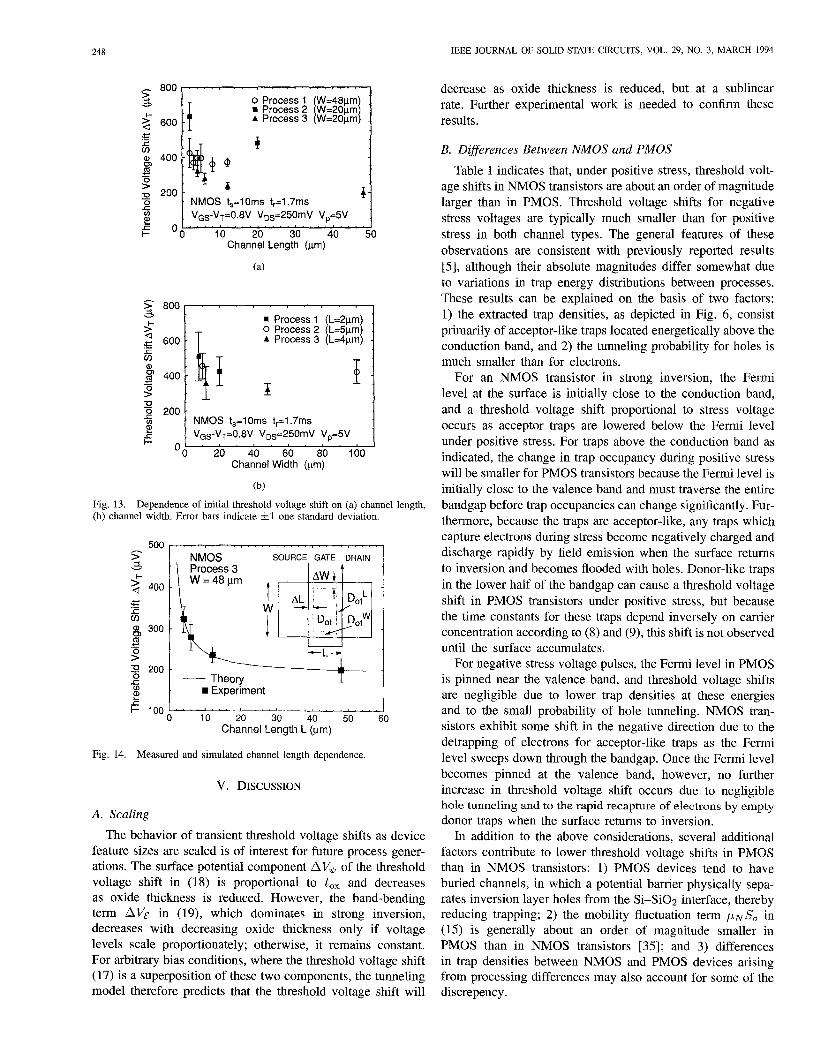
Fig. 12 plots the initial threshold voltage shift versus tem-perature, together with simulations using the two-step lmodeland the lattice relaxation model with cot-related mobility
fluctuations. A uniform distribution of activation energies EA
was assumed, with SO = 0.01 V. slcm2 and PN = 500 cm2N.
s. The lattice relaxation model leads to an increasing thresh-
old voltage shift with temperature due to the activated timeconstant (9). However, this increase is offset by the negative
temperature coefficient of the correlated mobility term. The
NMOS (Process 2) W/L.500~m/5pm\\
‘\
=..
---- Lattice Relaxation Model
— Two-Step Model
300 I I-50 0 50 100 150
Temperature (Celsius)
Fig. 12. Initiat threshold voltge shift versus temperature,
data fall somewhere between the two simulated curves, and canbe explained equally well by either inelastic mechanism or by alinear combination of the two. Experimentally, the temperaturecoefficient for positive stress varies from approximately – 0.1to –3.25 pVI°C.
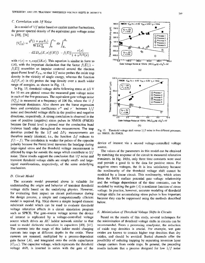
G. Channel Width and Length
The threshold voltage shift is observed to decrease slightlywith increasing channel length and width, as shown in Fig.13. This can be explained as an edge effect, due to highertrap densities around the periphery of the gate oxide arisingfrom damage created during implantation of the source–drain
regions or from higher trap densities in the field oxide thatforms the bird’s beak [39]. Consider a uniform trap densityDOt in the interior region of the gate oxide, as shown inthe inset of Fig. 14, and strips of width AW along thebird’s beak and AL bordering on the source–drain regionsin which the trap density has enhanced values DOT andD~t, respectively. The threshold voltage shift is proportional
to the total charge divided by the total oxide capacitance,
integrated over all energies and depths. Since the above theoryassumed a trap density which was uniform over area, (14)must be modified by the substitution shown at the bottomof this page. For AW << W and AL << L, which isvalid for the devices used in this study, AVT as calculatedin (14) must therefore be multiplied by a geometry-dependentprefacto~
AV;(L, W) = [1+ ; + ~] AVT (22)
where 71 = 2ALD~t/DOt, VW = 2AWD~/DOt, and AVTis the asymptotic value of the threshold voltage shift for largeL and W. Simulations using (22) with Tz = 1.24 ~m areplotted in Fig. 14, and show excellent agreement with thedata.
D.t WL DOt(W – 2AW)(L – 2AL) + 2WALD~t + 2AW(L – 2AL)D~
COXWL * G’oXWL
248 IEEE JOURNAL OF SOLID-STATE CIRCUITS, VOL. 29, NO. 3, MARCH 1994
.=-cu) :$ I$ 400
~+ @g0
; 200 -&
NMOS t~=l Oms tr=l .7ms4-
-cIng VG~-VT=0.8V VD~=250mV VP=5V
F 00 10 20 30 40 50Channel Length (~m)
(a)
~ 8001 I~
1 z Process 1 (L=2Lm)>+ o process 2 L=5~m)2 soo T IA Process 3 L=4um) 1
Lu
. . .5 NMOS t,=l Oms trl .7ms
~VG~-VT=0.8V VD~=250mV VP=5V
e00 20 40 60 80 100
Channel Width (Lm)
(b)
Fig. 13. Dependence of initial threshold voltage shift on (a) channel length,(b) channel width. Error bars indicate +1 one standard deviation.
NMOS SOURCE GATE ORAIN
I
Process 3 i
W=48pm AW ~
II *I ;--”~Do:f’
1 II u~t:...... DOtw
.-E Experiment
o 10 50Ch%nel L%gth L~Lm)
Fig. 14. Measured and simulated channel length dependence.
V. DISCUSSION
A. Scaling
)
The behavior of transient threshold voltage shifts as device
feature sizes are scaled is of interest for future process gener-ations. The surface potential component AV4 of the thresholdvoltage shift in (18) is proportional to tox and decreasesas oxide thickness is reduced. However, the band-bendingterm AV& in (19), which dominates in strong inversion,decreases with decreasing oxide thickness only if voltagelevels scale proportionately; otherwise, it remains constant.For arbitrary bias conditions, where the threshold voltage shift(17) is a superposition of these two components, the tunnelingmodel therefore predicts that the threshold voltage shift will
decrease as oxide thickness is reduced, but at a sublinearrate. Further experimental work is needed to confirm theseresults.
B. Differences Between NMOS and PMOS
Table I indicates that, under positive stress, threshold volt-age shifts in NMOS transistors are about an order of magnitudelarger than in PMOS. Threshold voltage shifts for negative
stress voltages are typically much smrdler than for positive
stress in both channel types. The general features of theseobservations are consistent with previously reported results[5], although their absolute magnitudes differ somewhat dueto variations in trap energy distributions between processes.These results can be explained on the basis of two factors:
1) the extracted trap densities, as depicted in Fig. 6, consistprimarily of acceptor-like traps located energetically above theconduction band, and 2) the tunneling probability for holes ismuch smaller than for electrons.
For an NMOS transistor in strong inversion, the Fermilevel at the surface is initially close to the conduction band,
and a threshold voltage shift proportional to stress voltageoccurs as acceptor traps are lowered below the Fermi levelunder positive stress. For traps above the conduction band asindicated, the change in trap occupancy during positive stresswill be smaller for PMOS transistors because the Fermi level isinitially close to the valence band and must traverse the entirebandgap before trap occupancies can change significantly. Fur-thermore, because the traps are acceptor-like, any traps whichcapture electrons during stress become negatively charged anddischarge rapidly by field emission when the surface returnsto inversion and becomes flooded with holes. Donor-like traps
in the lower half of the bandgap can cause a threshold voltageshift in PMOS transistors under positive stress, but becausethe time constants for these traps depend inversely on carrierconcentration according to (8) and (9), this shift is not observeduntil the surface accumulates.
For negative stress voltage pulses, the Fermi level in PMOSis pinned near the valence band, and threshold voltage shiftsare negligible due to lower trap densities at these energiesand to the small probability of hole tunneling. NMOS tran-sistors exhibit some shift in the negative direction due to thedetrapping of electrons for acceptor-like traps as the Fermilevel sweeps down through the bandgap. Once the Fermi level
becomes pinned at the valence band, however, no furtherincrease in threshold voltage shift occurs due to negligiblehole tunneling and to the rapid recapture of electrons by empty
donor traps when the surface returns to inversion.In addition to the above considerations, several additional
factors contribute to lower threshold voltage shifts in PMOSthan in NMOS transistors: 1) PMOS devices tend to haveburied channels, in which a potential barrier physically sepa-rates inversion layer holes from the Si–SiOa interface, therebyreducing trapping; 2) the mobility fluctuation term MNSO in
(15) is generally about an order of magnitude smaller inPMOS than in NMOS transistors [35]; and 3) differencesin trap densities between NMOS and PMOS devices arisingfrom processing differences may also account for some of thediscrepancy.
TEWKSBURY AND LEE: TRANSIENT THRESHOLD VOLTAGE SHIFTS IN MOSFET’S 249
C. Correlation with IJ Noise
In a model of l/~ noise based on carrier number fluctuations,the power spectral density of the equivalent gate voltage noiseis [20], [34]
//qz(l + ~~so) ‘“x ~x “(%s) = ~Lc,
0x o E.
. dEDot(E, z)f(fq[l– j(fq]1 + y2( ~
with r(x) = TOexp(2Kx). This equation is similar in form to
(14), with the important distinction that the factor ~(-E)[l -~(11)] resembles an impulse centered around the electronquasi-Fermi level EFn, so that l/~ noise probes the oxicle trap
density in the vicinity of single energy, whereas the functionAj(E, r) in (4) probes the trap density over a much wider
range of energies, as shown in Fig. 11.In Fig. 15, threshold voltage shifts following stress at +5 V
for 10 ms are plotted versus the measured gate voltage noisein each of the five processes. The equivalent gate voltage noise
(V&~) is measured at a frequency of 100 Hz, where the 1/ fcomponent dominates. Also shown are the linear regressionlines and correlation coefficients r+ and r- between l/~noise and threshold voltage shifts in the positive and negative
directions, respectively. A strong correlation is observed in thecase of positive (negative) stress pulses in NMOS (PMOS)
because the Fermi level is pinned near the conduction band(valence band) edge throughout the measurement. The trapdensities probed by the l/f and AVT measurements are
therefore nearly identical, i.e., the function A j reduces to~(1 – ~). The correlation is weaker for pulses of the oppositepolarity because the Fermi level traverses the bandgap cluringlarge-signal stress and the threshold voltage measurement isaffected by traps far outside the range which contribute 10 l/fnoise. These results support the conclusion that 1/$ noise andtransient threshold voltage shifts aresignal manifestations, respectively,mechanism.
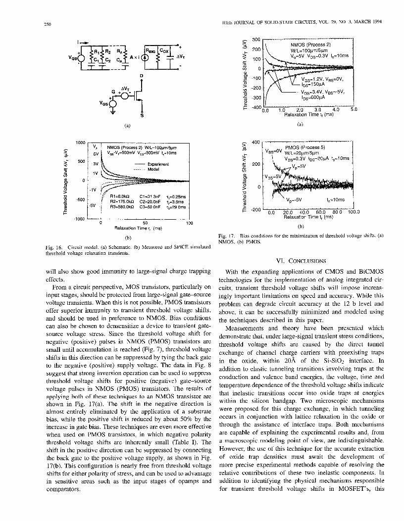
D. Circuit Model
The accurate model presented
simply small- and ku-ge-of the same underlying
above is valuable forunderstanding the origin and behavior of transient thresholdvoltage shifts based on the underlying physics. However,for evaluating their impact on circuit performance duringthe design process, a simple and computationally efficientmodel is required. Fig. 16(a) shows a simple Iumped element
subcircuit model which can be used to evaluate thresholdvoltage relaxation effects in a circuit simulation prclgramsuch as SPICE. The gate–source voltage across the deviceof interest is replicated by a voltage-controlled voltagesource which drives an RC ladder network similar tc) thatused to model dielectric relaxation in capacitors [40], [41].The currents into the rungs of this ladder model chargingcurrents into traps at different depths in the oxide. Thesecurrents are summed, multiplied by a process-dependentgain factor (A), and integrated onto the oxide capacitance(COX). The capacitor voltage, which represents the thresholdvoltage shift, is inserted in series with the gate of the
900.0 - NMOS VQS-VT. O 5i VN. 0.5V ~. 10mi
:s 7000
:0
■~ Vp = +5V
r+ =092.: 500,0 + ■
‘u
:: 3000 - ●
,<n~
Q Process 1❑ Process2
mA Process3g 1000
~ v Process4
-~ -100,00 Process5
:>-a
&
-g .300.0
~o Q) ❑Vp = -5V
%~ .500,0 r-=063
❑
-700.$!01000 200.0 300.0
14000 500,0
Gate Voltage Nose at 100Hz (WLCoJq) <VG2SnV
(a)
PMOS VGS-VT = -0,5V VDS = -0.5V t,= 10rns
m “/—
i+’ Igqm
5r-----Vp = -5Vr- = 0,66 ❑
I3 20 40 6.0 60 100
Gate Voltage Noise at 10OHZ(WLCOx/q) <VG2> nV
(b)
Fig. 15. Threshold voltage shift versus 1/f noise in five different processes.(a) NMOS, (b) PMOS.
device of interest via a second voltage-controlled voltagesource.
The values of the parameters in this model can be obtained
by matching the response of the circuit to measured relaxationtransients. In Fig. 16(b), only three time constants were usedand provide a good fit to the data for positive stress. Fornegative stress voltages, the fit is less satisfactory becausethe nonlinearity of the threshold voltage shift cannot bemodeled by a linear circuit. This nonlinearity, which arisesfrom the MOS surface potential gate–voltage relationshipand the voltage dependence of the time constants, can bemodeled by making the gain (A) a nonlinear function of stressvoltage. l[n practice, however, accurate modeling of thresholdvoltage shifts for accumulating stress pulses is less importantbecause they can be suppressed using the methods describedbelow.
E. Minimization of Threshold Voltage Shifts in Circuits
Based on the results of this study, several techniques for
the minimization of threshold voltage shifts in circuits can berecommended. From a processing standpoint, the reductionof oxide trap densities is crucial. For example, wet gateoxides are known to contain higher trap densities than dryoxides, and should be avoided. Buried channels offer thepossibility of reducing trapping by separating inversion layercharge carriers from oxide traps. In general, the precedingresults indicate that a process designed for low 1/~ noise
250 IEEE JOURNAL OF SOLID-STATE CIRCUITS, VOL. 29, NO 3. MARCH 1994
(a)
1000Vp \ NMOS(Process 2) W/L=l00VM/5pM
s~ 5V VG~-VT=500mVVD~=300mV t,=l Oms
>’4g ------ Model
6 Iv
um o - . . . . . . . . . . . . . . . .g
s~$ R2=175,0ki2 C2=20.OnF t,=3.5ms$ -5V / R3=580.0k12 C3.50 OnF ‘13.29 Oms
z-1000 I ~ 1
Q 50 100
Relaxation Time t, (ins)
(b)
~ 300
% 200>“: 100z(n ow~ .100
; -2005% -300~
E -4000.0 1.0 2.0 3.0 4.0 5.0Relaxation Time t, (ins)
(a)
~ 400~
>+
: 200%arng
:0~gp
s -2000.0 20.0 40.0 60.0 800 100.0
Relaxation Time tr (ins)
(b)
Fig. 17. Bias conditions for the minimization of threshold voltage shifts. (a)NMOS. (b) PMOS.
Fig. 16. Circuit model. (a) Schematic. (b) Measured and SPICE simulatedthreshold voltage relaxation transients.
VI. CONCLUSIONS
will also show good immunity to large-signal charge trappingeffects.
From a circuit perspective, MOS transistors, particularly oninput stages, should be protected from large-signal gate–sourcevoltage transients. When this is not possible, PMOS transistorsoffer superior immunity to transient threshold voltage shifts,and should be used in preference to NMOS. Bias conditionscan also be chosen to densensitize a device to transient gate-source voltage stress. Since the threshold voltage shift fornegative (positive) pulses in NMOS (PMOS) transistors are
small until accumulation is reached (Fig. 7), threshold voltageshifts in this direction can be suppressed by tying the back gateto the negative (positive) supply voltage. The data in Fig. 8suggest that strong inversion operation can be used to suppressthreshold voltage shifts for positive (negative) gate–sourcevoltage pulses in NMOS (PMOS) transistors. The results of
aPPIYing botb of these techniques to an NMOS transi Stor at-eshown in Fig. 17(a). The shift in the negative direction isalmost entirely eliminated by the application of a substratebias, while the positive shift is reduced by about 50% by theincrease in gate bias. These techniques are even more effectivewhen used on PMOS transistors, in which negative polaritythreshold voltage shifts are inherently small (Table I). Theshift in the positive direction can be suppressed by connectingthe back gate to the positive voltage supply, as shown in Fig.17(b). This configuration is nearly free from threshold voltageshifts for either polarity of stress, and can be used to advantagein sensitive areas such as the input stages of opamps andcomparators.
With the expanding applications of CMOS and BiCMOS
technologies for the implementation of analog integrated cir-
cuits, transient threshold voltage shifts will impose increas-
ingly important limitations on speed and accuracy. While thisproblem can degrade circuit accuracy at the 12 b level and
above, it can be successfully minimized and modeled using
the techniques described in this paper.Measurements and theory have been presented which
demonstrate that, under large-signal transient stress conditions,
threshold voltage shifts are caused by the direct tunnel
exchange of channel charge carriers with preexisting traps
in the oxide, within 20~ of the Si-SiOz interface. In
addition to elastic tunneling transitions involving traps at the
conduction and valence band energies, the voltage, time and
temperature dependence of the threshold voltage shifts indicate
that inelastic transitions occur into oxide traps at energieswithin the silicon bandgap. Two microscopic mechanismswere proposed for this charge exchange, in which tunnelingoccurs in conjunction with lattice relaxation in the oxide or
through the assistance of interface traps. Both mechanismsare capable of explaining the experimental results and, from
a macroscopic modeling point of view, are indistinguishable.
However, the use of this technique for the accurate extraction
of oxide trap densities must await the development ofmore precise experimental methods capable of resolving the
relative contributions of these two inelastic components. Inaddition to identifying the physical mechanisms responsible
for transient threshold voltage shifts in MOSFET’s, this
TEWKSBURY AND LEE TRANSIENT THRESHOLD VOLTAGE SHIFTS IN MOSFET’S 251
work has applications to explaining drifts in II-VI iind II-
V MISFET’s [42], [43] and to modeling the effects of oxide
traps on other large-signal measurements such as deep-level
transient spectroscopy (DLTS) [12], [25] and charge pumping
[44].
APPENDIX
Assumption 2) of Section III-D implies that
f(J% – q:z,Ei7) – f(-E, – qtofr,Em))
{
+1 13F + q~$ S Et < EFO + qc%r (}L > o)—— –1 EFO +q&r ~ Et < EF+q~z (T2 < o)
o otherwise.
Substituting this result into (14) and invoking the remainingassumptions of Section III-D, the threshold voltage shift is
HqDot ‘Ox EFo+q&, z
AVT(t., tT) = + ~0x o EF +q&x
. [1_ ~-ts/Ts(z)]e-tr/Tr(z)~~t~z
where the plus sign applies for VP > 0 and the minus signfor VP <0. The energy integration can be evaluated trivially
to yield two terms:
Jt
AVV = + +(E.O - E.) 0’0x o
(23)
AV& = + 9(E0 –&) /tOx x[l – e-tsi’s]e-trj”’-dx.0x o
(24)
The integral in (23) can be carried out by changing the variable
of integration from z to ~ = t/TO exp( –2Kz) and recognizingthat
t
/[
oxexp 1–~exp(–2Kz) d~
o TO
1
-/
tlro ~–-y
—— —dy2K t/Tl Y
‘*H3-EIE)Iwhere T1 = TOexp(2KtOX) and El(z) is the exponentialintegral function [45]
El(z) =/
W e–z—dx
z x
which has the properties that limz~~ El(z) = O and El (z) =–T – In z for small z, where ~ = 0.5772 is Euler’s constant.
Thus,
Av+ = + #&-&o – “){El(%)-E’(51)‘E’(:+:)+E’(5-:)}‘2’)
Since To. and TOTare on the order of 10-10 s, it is alwaysthe case in our measurements that t, >> T.. and tr :> T..so that the second and third exponential integrals in (25)
can be neglected. Since to. > 250 ~ while the maximumtunneling depth is only 10–20 ~, the time constants ~1~ =
~0~exp(2KtOX) and rlr = TO.exp(2KtOX ) are very largerelative to time scales of the measurement, so that, using
the series expansion of the exponential integral, (25) can berearranged to give (18).
The integral in (24) can be readily evaluated by noting that
d ‘Ox--J Jtox‘t/Tdz= dx~e–t/T_.
dt ~ ‘e o r
Using the substitution u = t/r,
(26)
where the lower and upper integration limits in (26) have beenreplaced by zero and infinity, respectively, since TO<< t<< T1
for the time scales of interest. Thus,
It0,
xe ‘thdx = _
o +4+2(:)+’1”(:)so that AVS is
‘Av0x{+2(5+5-’”2(5)1‘v&=4K2COX
“In (:+:)-in (:)1}(27)
which can be rewritten, by simple algebraic manipulations, as(19).
TheM.I.T.
ACKNOWLEDGMENT
authors wish to thank Analog Devices Inc. and the
Microsystems Technology Laboratories for fabrication
of the devices used in this study. They especially thank Prof.
S. D. Senturia and Prof. C. G. Sodini at M.I.T. for technicalassistance and numerous helpful discussions.
[1]
[2]
[3]
[4]
[5]
[6]
[7]
lWFt3RENCES
I. A. Young and D. A. Hodges, “MOS switched-capacitor arrafogsampled-data direct-form recursive filters,” IEEE J Solid-State Circuits,vol. SC-14, pp. 102G1033, Dec. 1979.R. Castello and P. R. Gray, “A high-performance rnicropowerswitched-capacitor filter,” IEEE J. Solid-State Circuits, vol. SC-20,pp. 1122–1 132, Dec. 1985.H.-S. Lee, D. A. Hodges, and P. R. Gray, “A self-calibrating 15 bitCMOS A/D converter,” IEEE J. Solid-State Circuits, vol. SC-19, pp.813-819, Dec. 1984.P. W. Li, M. J. Chkr, P. R. Gray, and R. Castello, “A ratio-independentalgorithmic analog-to-dlgltal conversion technique:’ IEEE J. Solid-StateCimuits, vol. SC-19, pp. 828–836, Dec. 1984.T. L. Tewksbury, H.-S. Lee, and G. A. Miller, “The effects of oxidetraps on the large-signat transient response of analog MOS circuits,”IEEE J. Solid-State Circuits, VOL 24, pp. 542-544, Apr. 1989.T. L. Tewksbury and H.-S. Lee, “Characterization, minimization andmodeling of transient threshold voltage shifts in MOSFETS,” in Proc.IEEE Custom Integrated Circuits Confi, San Diego, CA, May 1993, pp.14.4.1-14.4.4.L Lnndstrom, S. Christensson, and C. Svensson, “Carrier trappinghysteresis in MOS transistors,” Plays. Status Solid (A), vol. 1, no. 395,pp. 395-407, 1970.
252 IEEE JOURNAL OF SOLID-STATE CIRCUITS, VOL. 29, NO. 3, MARCH 1994
[8]
[9]
[10]
[11]
[12]
[13]
[14]
[15]
[16]
[17]
[18]
[19]
[20]
[21]
[22]
[23]
[24]
[25]
[26]
[27]
[28]
[29]
[30]
[31]
[32]
[33]
[34]
[35]
P. Rossel, H. Martinet, and A. Serhal, “Instabilities temporelles destransistors MOS-1,” Solid-Sfate Electron., vol. 13, pp. 257–268, 1970.“Instabilities temporelles des transistors MOS-11,” Solid-State Electron.,vol. 13, pp. 425S438, 1970.E. H. Snow and B. E. Deal, “Polarization effects in insulating filmson silicon—A review,” Trans. Met. Sot. AIME, vol. 242, pp. 512–523,Mar. 1968.P. Cuevas, “A simple explanation for the apparent relaxation effectassociated with hot-carrier phenomenon in MOSFETS,” IEEE ElectronDevice Lett., vol. 9, pp. 627–629, Dec. 1988.D. Vuillaume, J. C. Bourgoin, and M. Lannoo, “Oxide traps in Si-SiO~ structures characterized by tunnel emission with deep-level transientspectroscopy,” Phys. Rev. B, vol. 34, pp. 1171–83, July 1986.D. J. DiMaria, “Trap creation in silicon dioxide produced by hotelectrons,” J. Appl. Phys., vol. 65, no. 6, pp. 2342–2356, 1989.“Defects and impurities in thermal SiOz ,“ in The Physics of Si02 andIts Interfaces, S. T. Pantelides, Ed. New York Pergamon, 1978, pp.160-178.S. K. Lai and D. R. Young, “Effects of avalanche injection of electronsinto silicon-dioxide—Generation of fast and slow interface states,” .J.Appl. Phys., vol. 52, pp. 6231-6240, Oct. 1981.F.-C. Hsu and S. Tam, “Relationship between MOSFET degradation andhot-electron-induced interface-state generation,” IEEE Electron DeviceLett., vol. EDL-8, pp. 50-52, Feb. 1984.M. Bourcerie, B. S. Doyle, J. C. Marchetaux, J. C. Soret, and A. Boudou,“Relaxable damage in hot-carrier stressing of n-MOS transistors—Oxidetraps in the near interracial region of the gate oxide,” LEEE Trans.Electron Devices, vol. 37, pp. 708-717, Mar. 1990.B. S. Doyle, M. Bourcerie, J.-C. Marchetaux, and A. Boudou, “Re-laxation effects in NMOS transistors after hot-carrier stressing,” IEEEElectron Device Lett., vol. EDL-8, pp. 234236, May 1987.F. P. Heiman and G. Warfield, “The effects of oxide traps on the MOScapacitance,” IEEE Trans. Electron Devices, vol. ED-12, pp. 167–178,Apr. 1965.S. Cbrktensson, I. Lundstrom, and C. Svensson, “Low frequency noisein MOS transistors,” Solid-State Electron, vol. 11, pp. 797–8 12, 1968.B. Balland and P, Plnard, “Interracial tunnel interaction in MOSelements in depletion,” Phys, Status Solidi (A), vol. 47, pp. 25 1–258,1978.P. van Staa, H. Rombach, and R. Kassing, “Time-dependent responseof interface states in indhm phosphide metal-insulator-semiconductorcapacitors investigated with constant-capacitance deep-level transientspectroscopy,” J. Appl. Phys., vol. 54, pp. 4014-4021, July 1983.V. Lakshmanna and A. S. Vengurlekar, “Logarithmic detrapping re-sponse for holes injected into SiOz and the influence of thermalactivation and electric fields,” 1 Appl. Phys., vol. 63, no. 9, pp.4548-4554, 1988.T. L. Tewksbury, “Relaxation effects in MOS devices due to tunnelexchange with near-interface oxide traps,” Ph.D. dissertation, Massa-chusetts Inst. Technol., 1992.H. Lakfmdi, D. Vuillaume, and J. C. Bourgoin, “Spatial and energeticdistribution of Si-SiOz near-interface states,” Phys. Rev. B, vol. 38, pp.13124–13132, Dec. 1988.L Lundstriim and C. Svensson, “Tunneling to traps in insulators,” JAppl. Phys., vol. 43, pp. 5045-5047, Dec. 1972.J. R. Chelikowsky and M. Schluter, “Electron states in a-quartz: A self-consistent pseudopotential calculation,” Phys. Rev. B, vol. 15, no. 8, pp.40204029, 1977.H. S. Fu and C. T. Sah, “Theory and experiments on surface 1/f noise,”IEEE Trans. Electron Devices, vol. ED-19, pp. 273–285, Feb. 1972.W. Shockley and W. Read, “Statistics of the recombination of holes andelectrons,” Plrys. Rev., vol. 87, no. 835, pp. 835–842, 1952.M. Lax, “Cascade capture of electrons in solids,” Phys. Rev., vol. 119,
PP. 1502–1523, Sept. 1960.D. V. Land and C. H. Henry, “Nonradiative recombination at deeplevels in GaAs and Gap by lattice-relaxation multiphonon emission,”P1-zys.Rev. Lett., vol. 35, Dec. 1975.M. J. Kirton and M. J. Uren, “Noise in solid-state rnicrostructures:A newperspective on individual defects, interface states and low-frequency(l/f) noise,” Adv. Phys., vol. 38, no. 4, pp. 367+68, 1989.E. H. Nicollian and J. R. Brews, &fOS (Metal Oxide Semiconductor)Physics and Technology. New York: Wiley, 1982.R. Jayaraman and C. G. Sodlni, “A 1/f noise technique to extract theoxide trap density near the conduction band edge of silicon,” IEEETrans. Electron Devices, vol. 36, pp. 1773–1782, 1989.B. J. Gross and C. G. Sodini, “1/f noise in MOSFETS with ultrathhrgate dielectrics,” in IEDM Tech. Dig., Dec. 1992, pp. 88 1–884.
[36]
[37]
[38]
[39]
[40]
[41]
[42]
[43]
[44]
[45]
Z. Celik-Butler and T. Y. Hsiang, “Spectral dependence of 1 / f ~ noiseon gate bias in n-MOSFETs,” Solid-State Electron., vol. 30, no. 4, pp.419-423, 1987.N. Hwang, B. S. S. Or, and L. Forbes, “Tunneling and thermal emissionof electrons from a distribution of deep traps in Si-Oz ,“ IEEE Trans.Electron Devices, vol. 40, no. 6, pp. 1100, 1993.N. Shiono, M. Shimaya, and O. Nakajima, “Charge character of interfacetraps at the Si02 interface,” Appl, Phys. Lett,, vol. 48, no. 17, pp.11~9-1131, 1986.A. Balasinskl and T. Ma, “Enhanced electron trapping near channeledges in NMOS transistors,” IEEE Trans. Electron ~~vices, vol. 39, pp.1680-1686, July 1992.P. C. Dow, “An analysis of certain errors in electronic differentialanalyzers II—Capacitor dielectric absorption,” IRE Trans. Electron.Cornput., Pp. 17-22, Mar. 1958.J. W. Fattarnso, M. D. Wit, G. Warwar, K.-S. Tan, and R. K. Hes-ter, “The effect of dielectric relaxation on charge-redistribution A/Dconverters,” IEEE J. Solid-State Circuits, vol. 25, pp. 1550–1561, Dec.1990,H. Koelmans and H. C. D. Graaff, “Drift phenomena in CdSe thhr filmFET’s,” Solid-State Electron., vol. 10, pp. 997-1005, 1967.S. J. Prasad and S. J. T. Owen, “The InP-SiOz interface: Electron tunnel-ing into oxide traps,” in Dielectric Films on Compound Semiconductors,Electrochem. Sot., 1985, vol. 86-3, pp. 23-32.M. Declercq and P. Jespers, “Analysis of interface properties in MOStransistors by means of charge pumping measurements,” Rev. HF Acts.Techn. Belgica., vol. 9, 244-253, 1974.M. Abramowitz and I. A. Stegun, Handbook ofMathematical Functions,10th ed, Washington, DC: Nat. Bureau Standards, 1972, ch. 5, p. 228.
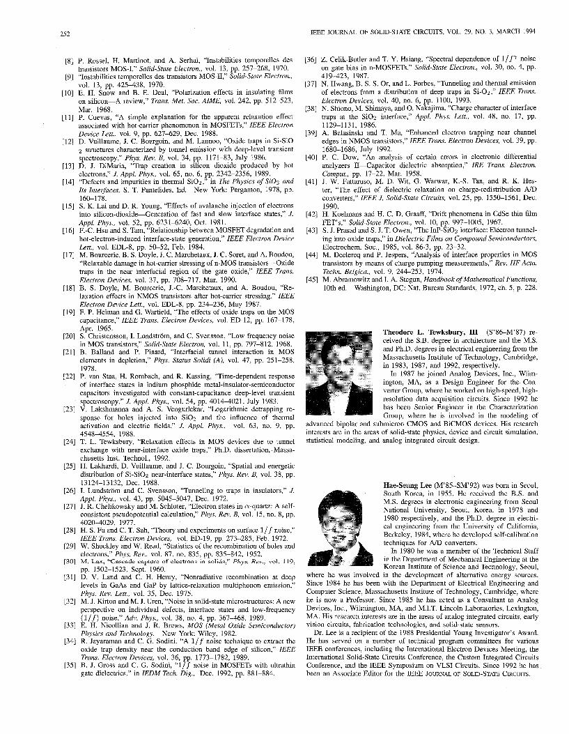
Theodore L. Tewksbury, III (S’86-M’87) re-ceived the S.B. degree in architecture and the M.S.and Ph.D. degrees in electrical engineering from theMassachusetts Institute of Technology, Cambridge,in 1983, 1987, and 1992, respectively.
In 1987 he joined Analog Devices, Inc., Wilm-ington, MA, as a Design Engineer for the Con-verter Group, where he worked on high-speed, high-resolution data acquisition circuits. Since 1992 hehas been Senior Engineer in the CharacterizationGroup, where he is involved in the modeling of
advanced bipolar and submicr& CMOS and BiCMOS devices. Hk rese-mchinterests are in the areas of solid-state physics, device and circuit simulation,statistical modeling, and analog integrated circuit design.
Hae-Seung Lee (M’85–SM’92) was born in Seoul,South Korea, in 1955. He received the B.S. andM.S. degrees in electronic engineering from SeoulNational University, Seoul, Korea, in 1978 and1980 respectively, and the Ph.D. degree in electri-cal engineering from the University of California,Berkeley, 1984, where he developed self-calibrationtechniques for A/D converters.
In 1980 he was a member of the Technical Staffin the Department of Mechanical Engineering at theKorean Institute of Science and Technology, Seoul,
where he was involved in the development of alternative energ~ sources.Since 1984 he has been with the Department of Electrical Engineering andComputer Science, Massachusetts Institute of Technology, Cambridge, wherehe is now a Professor. Since 1985 he has acted as a Consultant to AnalogDevices, Inc., Wilmington, MA, and M.I.T. Lincoln Laboratories, Lexington,MA. His research interests are in the areas of analog integrated circuits, esulyvisiou circuits, fabrication technologies, and solid-state sensors.
Dr. Lee is a recipient of the 1988 Presidential Young Investigator’s Awzn-d.He has served on a number of technical program committees for variousIEEE conferences, including the International Electron Devices Meeting, theInternational Solid-State Circuits Conference, the Custom Integrated CircuitsConference, and the IEEE Symposium on VLSI Circuits. Since 1992 he hasbeen an Associate Editor for the IEEE JOURNALOF SOLID-STATECRCUITS.