Embed Size (px)
Citation preview
ARTICLE IN PRESS
0168-9002/$ - se
doi:10.1016/j.ni
�CorrespondE-mail addr
Nuclear Instruments and Methods in Physics Research A 565 (2006) 221–226
www.elsevier.com/locate/nima
Characterization of a thinned back illuminated MIMOSA V sensor as avisible light camera
Antonio Bulgheronia,b,�, Michele Biandac, Massimo Cacciab,d, Chiara Cappellinid,Aldo Mozzanicad, Renzo Ramellic, Fabio Risigoa
aUniversita degli Studi di Milano, Milano, ItalybIstituto Nazionale di Fisica Nucleare Sez. di Milano, Milano, Italy
cIstituto Ricerche Solari Locarno, Locarno, SwitzerlanddUniversita dell’Insubria, Como, Italy
Available online 15 June 2006
Abstract
This paper reports the measurements that have been performed both in the Silicon Detector Laboratory at the University of Insubria
(Como, Italy) and at the Instituto Ricerche SOlari Locarno (IRSOL) to characterize a CMOS pixel particle detector as a visible light
camera. The CMOS sensor has been studied in terms of Quantum Efficiency in the visible spectrum, image blooming and reset
inefficiency in saturation condition.
The main goal of these measurements is to prove that this kind of particle detector can also be used as an ultra fast, 100% fill factor
visible light camera in solar physics experiments.
r 2006 Elsevier B.V. All rights reserved.
PACS: 85.60.Gz; 29.40.Gx
Keywords: CMOS imager; Spectral response; Quantum Efficiency; Antiblooming; Image lag
1. Introduction
For a long time, Charge Coupled Devices (CCD) havebeen leading the way in the field of electronics camera forall kinds of applications. Over many years, the develop-ment has been driven by an increasing market demand forlarger and larger pixel numbers and better image qualitythat no other technology could provide. However, interestin image sensors based on standard Complementary MetalOxide Semiconductor (CMOS) technology has grownsignificantly in the past years. CMOS-based imagers offersignificant advantages over CCDs such as system-on-chipcapability, standard commercially available technology,low power consumption and possibly lower cost [1,2].Moreover the possibility to readout only a reduced numberof sparsified pixels in the matrix makes CMOS imager anappealing CCD competitor especially in fast applications.
e front matter r 2006 Elsevier B.V. All rights reserved.
ma.2006.05.126
ing author. Universita degli Studi di Milano, Milano, Italy.
ess: [email protected] (A. Bulgheroni).
In the early days of the CMOS imager story, one of themain disadvantages was the limited fill factor1 due to thealuminum tracks connecting each pixel to the readoutelectronics and to the peripheral addressing circuitry.Furthermore, since in a CMOS imager the sensitive volumeis a few hundreds of micrometers deep from the waferbackplane, back illumination with visible photons washardly achievable.Since the fill factor is not an issue in high-energy
elementary particle tracking and imaging, physicistsadopted CMOS imagers, suitably modified to fulfill theirrequirements, as an attractive alternative solution to hybridpixel detectors and to CCD [3] in future High-EnergyPhysics (HEP) experiments.In HEP experiments, the main role of this kind of
sensors is the identification of a particle track through thedetermination of its collision point on several sensor layers
1This is defined as the ratio between the sensitive surface and the total
sensor area.
ARTICLE IN PRESS
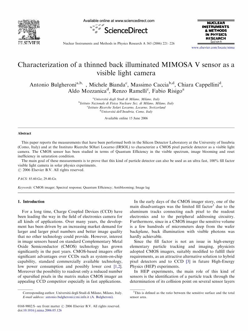
Fig. 1. A MIMOSA 5 sensor glued on a PCB adapter board.
Table 1
MIMOSA 5 main characteristics
Size 1020� 1024 pixels
Pixel pitch 17� 17mm2
Readout frequency 440MHz
Parallel analog output 4 channels
Frame readout time (@ 10MHz) 26ms
Technological process 0:6mm AMS
Epitaxial (sensitive) layer � 14mmConversion gain 7:3ADC=e�
CCE after thinning 50–60%
Camera gain 10:6ADC=e�
A. Bulgheroni et al. / Nuclear Instruments and Methods in Physics Research A 565 (2006) 221–226222
[4]. To reduce multiple scattering, the total thickness ofpassive and active material has to be kept as low aspossible. Moreover, removing insensitive layers increasesthe sensitivity to short-range particle. For this purpose, amajor development in the CMOS imager technology toremove the passive layer from the backplane has beenrecently carried out by the SUCIMA2 consortium [6–8].Due to the back thinning development, back illuminationvisible light detection is now achievable with a 100% fillingfactor and the CMOS imager potential can be fullyexploited. Because of a non-disclosure agreement signedbetween the SUCIMA consortium and an industrialpartner, technological details about the back thinningprocess cannot be revealed.
This paper describes the tests performed both at theSilicon Laboratory at the University of Insubria in Comoand at the Istituto Ricerche SOlari Locarno (IRSOL) inorder to characterize a thinned CMOS imager for visiblelight detection. The characterization experiments wereaimed to estimate the sensor Quantum Efficiency (QE) inthe visible part of the electromagnetic spectrum, the imageblooming and time latency in over saturation conditions.
2. The MIMOSA CMOS imager
The CMOS imager being characterized in these experi-ments belongs to a family of sensor called MinimumIonising MOS Active pixel sensor (MIMOSA) whosedevelopment was pioneered and still is driven by theLEPSI/IReS teams in Strasbourg [9]. A picture of thedevice under test is shown in Fig. 1 and its maincharacteristics are reported in Table 1.
The sensor has been tested with high-energy particles tostudy the detection and the charge collection efficiency(CCE), the spatial resolution and the charge to voltageconversion gain for different layout geometries.
Within the SUCIMA project, a major effort has beeninvested to push an extreme backthinning down to theepitaxial layer with an entrance window of �100 nm. Testsusing dedicated setups have shown that the thinned sensorsensitivity to short-range particles is clearly enhanced andamong all the detector performances only the CCE isreduced at the 50260% level after the post-processing [6].
3. Quantum Efficiency measurement
One of the most important feature of a visible lightdetector is its QE representing the number of chargecarriers produced by one impinging photon. The region ofinterest of the electromagnetic spectrum, corresponding tothe visible part and the near infra-read, is from 400 to850 nm thus the sensor QE dependence on wavelength
2Silicon Ultrafast Camera for electron and g sources in medical
applications (SUCIMA) is a completed project approved in the Fifth
Framework Program by the European Commission under the Contract
G1RD-CT-2001-00561 [5].
should be as flat as possible in that range and high enoughto assure an acceptable sensitivity level. From a theoreticalpoint of view [10], the QE wavelength dependency shouldreach a maximum when the corresponding photon energyis close to the forbidden energy gap.The output signal S measured in ADC units of a single
sensitive element exposed to a monochromatic photon maybe written as follows:
S ¼ FlZlgDtA (1)
where Fl is the photon flux for a given wavelength lmeasured in photons per second per unit of area, Zl is theQE at a given wavelength l measured in charge carriers perphoton, g is the sensor and amplification system overallconversion gain in ADC units per charge carrier, Dt is theexposure time, A is the surface of the sensitive element.Using this formula the QE of a sensor under investiga-
tion can be measured referring its signal to a detector withknown QE exposed to the same flux.
3.1. Experimental setup
Following the approach described in the previoussection, the QE of the MIMOSA 5 sensor has been studiedcomparing the output signal of both the CMOS and the
ARTICLE IN PRESS
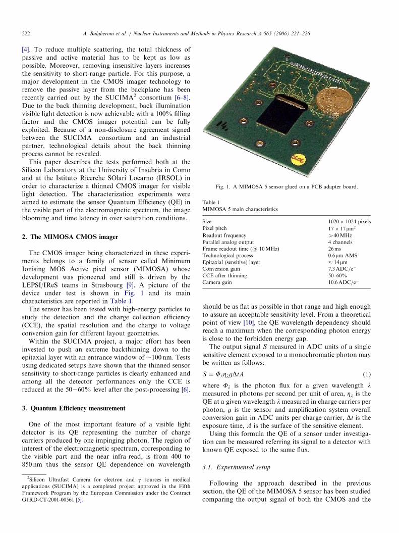
Fig. 2. Spectral response of the MIMOSA sensor compared with the
reference CCD. The dashed line represents the QE achievable with a 100%
CCE.
A. Bulgheroni et al. / Nuclear Instruments and Methods in Physics Research A 565 (2006) 221–226 223
Wright AT1 CCD camera available at IRSOL. Thespectral response and the main features of the referencecamera were made available by the producer.3 Takingadvantage of the use of the IRSOL spectrograph, sixnarrow spectral intervals of the solar light were recordedusing the two cameras at 400, 500, 630, 701, 760 and850 nm. Each spectral window has been chosen in a way tohave at least two absorption lines in the image in order todefine the linear function LðxÞ to translate the pixelposition on the MIMOSA sensor in the correspondingwavelength value according to the following Eq. (2)
LðxÞ ¼y1 � y2
x1 � x2
� �xþ
y2x1 � y1x2
x1 � x2
� �(2)
where
xi�!L
yi
are the two reference points.Particular care has been spent to keep the experimental
conditions in the two measuring setups as close as possible.For this purpose, during the data acquisition the solar lightintensity was monitored and only variations at the fewpercent level were recorded. Due to the readout scheme[11], the MIMOSA 5 exposure time was kept constant forall the spectral images while the CCD integration time wasproperly adjusted to best fit the dynamic range. To makethe output of the two cameras comparable, a normalizationfactor has been introduced to take into account thedifferent exposure time, the sensitive cell area and theoverall conversion gain. The last one is well known for theCCD camera, while for the MIMOSA the value obtainedwith the 55Fe calibration (Table 1) was used and thereduced CCE taken into account.
3.2. Data analysis
For each spectral region, 200 frames have been acquired,background subtracted and averaged to reduce the noisefluctuations. The two-dimensional images have beenprojected along the spectral axis that has been calibratedusing two absorption lines and comparing their positionswith the one reported on the National Solar Observatorysolar atlas.4 The obtained spectrum has been comparedwith the one acquired with the reference front illuminatedCCD. From the CCD measurements, the value of the solarphoton flux for each spectral window has been estimatedand used to calculate the QE of the MIMOSA 5 sensor.The obtained results are shown in Fig. 2.
As expected, the MIMOSA 5 sensor, being a backilluminated device, has a better QE than CCD in theultraviolet region while the thin sensitive layer is reducingthe sensibility to infrared radiation. The benefit arising
3http://www.e2v.com/datasheets/charge_coupled_devices_ccds/ccd62-
06ims.pdf.4Courtesy of NSO/Kitt Peak. The Fourier Transform Spectrometer
data used here were produced by NSF/NOAO.
from the thinning and the back illumination, i.e. the 100%fill factor, is somehow spoiled by the reduced CCE [7].Technologists are now considering some solutions torestore the almost complete CCE after the backthinning,this will result in a net improvement of the QE as shown bythe dashed line in Fig. 2, making the use of this kind ofsensor even more appealing.
4. Image blooming
In many experimental conditions, having images withregions particularly intense and other almost completelydark is not uncommon. This is true, for instance, whendealing with spectral images in which almost pure blackabsorption lines should be compared with a bright con-tinuum. In these cases, setting a proper exposure time is anissue because on one hand, it cannot be too short in order tohave enough statistics in the dark region and, on the otherhand, it cannot be too long to avoid saturation in the brightone. Moreover, in saturation condition, the brightest part ofthe image tends to grow in size (blooming) and in the worstcase it can occupy the full sensitive surface of the sensor.
ARTICLE IN PRESSA. Bulgheroni et al. / Nuclear Instruments and Methods in Physics Research A 565 (2006) 221–226224
The physical explanation of the image blooming effect insaturation condition can be related to the charge carrierdiffusion and in the case of CCDs to the charge transfermechanism. In CCD cameras, this is a well-known problemand several anti-blooming techniques have been implemen-ted the anti-blooming gate being the more common. Anti-blooming gates built into the CCD occupy about 30% ofthe pixel area. The result is a reduced fill factor andsensitivity. Furthermore, the area of the CCD occupied bythe anti-blooming gate leaves a significant gap betweenpixels, reducing the effective resolution of the sensor.
CMOS sensors should be naturally immune fromblooming since each pixel is directly connected to thereadout line switching on two selection transistors [2]. But,if the injected charge density in a region of the sensor is toohigh, charge carrier diffusion and electronic cross-talk mayresult in an image deformation and enlargement.
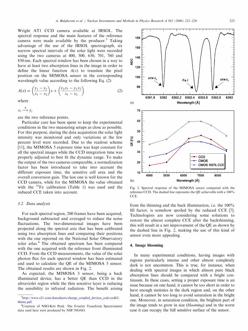
Fig. 3. Length of the detected hole image diameters as a function of the
light intensity. The light intensity has been spanned over eight orders of
magnitude. In the two flat regions, fluctuations in the radius length of one
or two pixels are not significant.
4.1. Experimental setup
A dedicated measuring setup has been assembled tocharacterize the MIMOSA image blooming when exposedto an over-saturating flux of visible light photons.
The setup consists of a He–Ne laser ðl ¼ 633 nmÞsource with a maximum emitted power of 10mW. Thelaser light passes through a polarizer–analyzer pair to havea variable light intensity. Due to the Gaussian-shapedintensity profile of the emitted light, only a small centralregion of the laser profile has been selected using a 1mmdiameter pin-hole to decrease the intensity inhomogeneity.The pin-hole has been kept as close as possible to theMIMOSA sensor in order to reduce the beam divergence.Moreover, to further reduce the laser intensity a spectralfilter can be inserted in the light path in between theanalyzer and the pin-hole.
An absolute measurement of the light intensity arriving onthe sensor surface is not trivial; to estimate it with a reason-able accuracy a part of the laser light has been collected by aphotodiode. The intensity measured by the photodiode isproportional to the one arriving on the MIMOSA.
4.2. Data analysis
Twenty images of the pin-hole corresponding to 10different polarizer–analyzer angles with and without thespectral filter have been acquired and analyzed. The lightintensity measured by the photodiode has been varied overeight orders of magnitude: with the first four decadesobtained with the spectral filter on the light path. The pin-hole image is an ellipse with an almost unitary degree ofeccentricity.5 The increased size of the hole image can be
5The pin-hole has been fabricated by drilling a hole in a squared 2 cm
edge aluminum plate. To avoid light reflection, a black adhesive tape has
been glued on both sides of the plate. To make the hole also in the tape,
the tip of a hot needle has been used and this could have been the origin of
the image eccentricity.
demonstrated considering the length of the two radii as afunction of the light intensity as shown in Fig. 3.The hole image size has been measured to be statistically
constant over the first four orders of magnitude while anincrease of �1:5 times in the radius length occurred overthe last four decades. The radius length increase startedwith the sensor saturation. It should be underlined that,since the sensor was designed for high-energy particletracking, its dynamic range is very limited and notoptimized for visible light applications.
5. Image lag
All sensitive devices are characterized by a certain deadtime during which they are not ready to detect a newphysical information because either they are being readoutor they are being reset to the initial condition. For sensorslike visible light cameras, another common fault is theimage latency, usually related to a non-completely efficientreset mechanism. Also human retina, for instance, is
ARTICLE IN PRESS
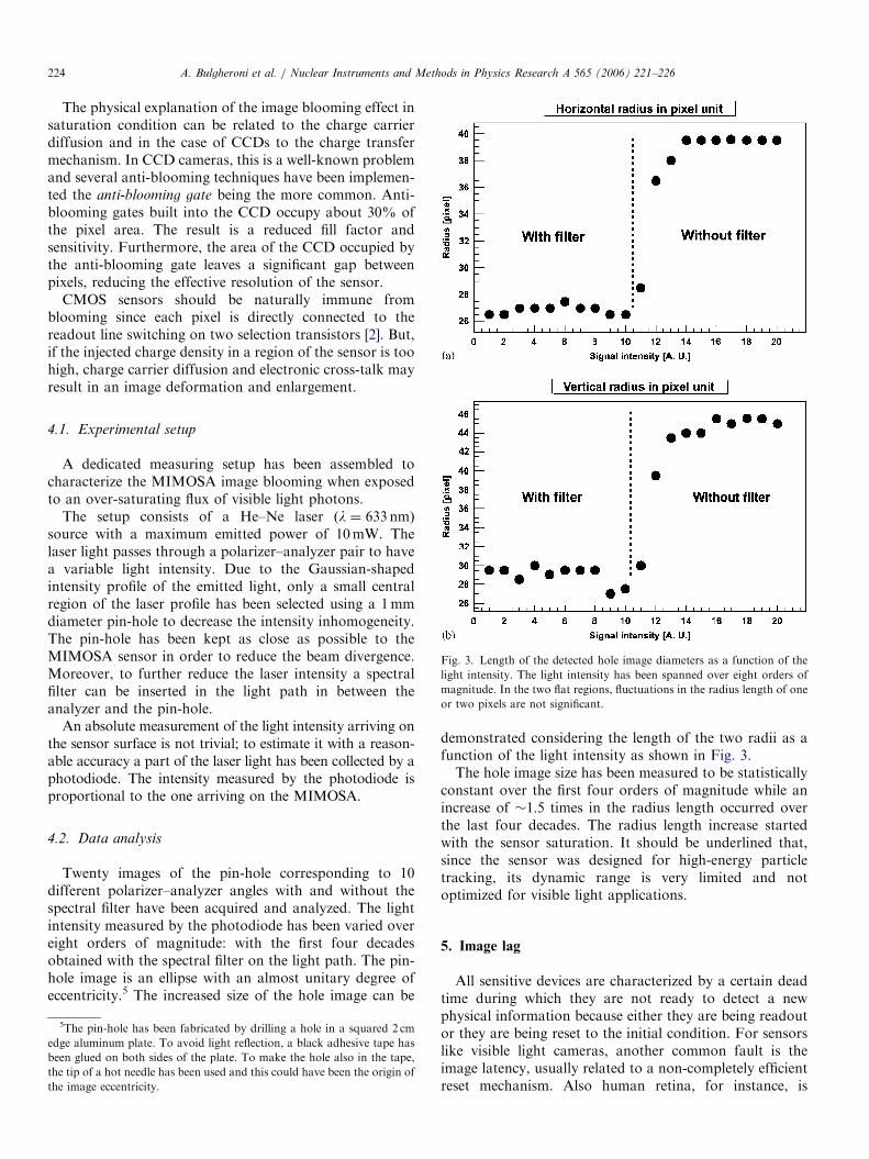
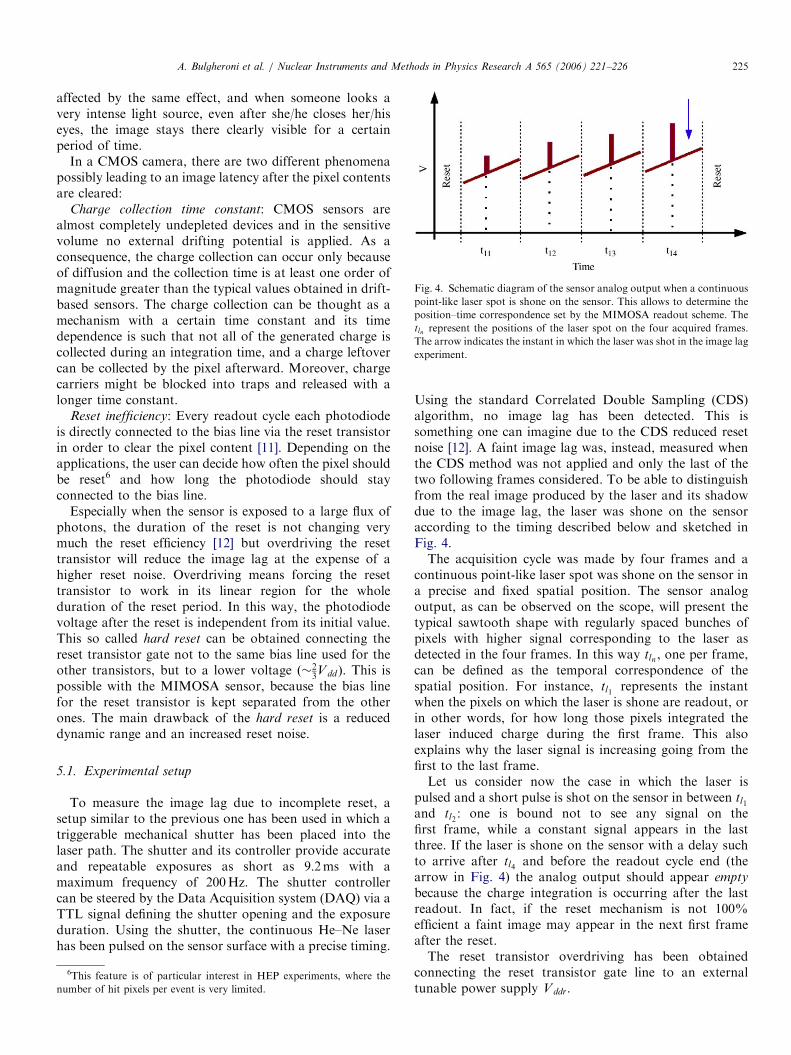
Fig. 4. Schematic diagram of the sensor analog output when a continuous
point-like laser spot is shone on the sensor. This allows to determine the
position–time correspondence set by the MIMOSA readout scheme. The
tln represent the positions of the laser spot on the four acquired frames.
The arrow indicates the instant in which the laser was shot in the image lag
experiment.
A. Bulgheroni et al. / Nuclear Instruments and Methods in Physics Research A 565 (2006) 221–226 225
affected by the same effect, and when someone looks avery intense light source, even after she/he closes her/hiseyes, the image stays there clearly visible for a certainperiod of time.
In a CMOS camera, there are two different phenomenapossibly leading to an image latency after the pixel contentsare cleared:
Charge collection time constant: CMOS sensors arealmost completely undepleted devices and in the sensitivevolume no external drifting potential is applied. As aconsequence, the charge collection can occur only becauseof diffusion and the collection time is at least one order ofmagnitude greater than the typical values obtained in drift-based sensors. The charge collection can be thought as amechanism with a certain time constant and its timedependence is such that not all of the generated charge iscollected during an integration time, and a charge leftovercan be collected by the pixel afterward. Moreover, chargecarriers might be blocked into traps and released with alonger time constant.
Reset inefficiency: Every readout cycle each photodiodeis directly connected to the bias line via the reset transistorin order to clear the pixel content [11]. Depending on theapplications, the user can decide how often the pixel shouldbe reset6 and how long the photodiode should stayconnected to the bias line.
Especially when the sensor is exposed to a large flux ofphotons, the duration of the reset is not changing verymuch the reset efficiency [12] but overdriving the resettransistor will reduce the image lag at the expense of ahigher reset noise. Overdriving means forcing the resettransistor to work in its linear region for the wholeduration of the reset period. In this way, the photodiodevoltage after the reset is independent from its initial value.This so called hard reset can be obtained connecting thereset transistor gate not to the same bias line used for theother transistors, but to a lower voltage ð�2
3V dd Þ. This is
possible with the MIMOSA sensor, because the bias linefor the reset transistor is kept separated from the otherones. The main drawback of the hard reset is a reduceddynamic range and an increased reset noise.
5.1. Experimental setup
To measure the image lag due to incomplete reset, asetup similar to the previous one has been used in which atriggerable mechanical shutter has been placed into thelaser path. The shutter and its controller provide accurateand repeatable exposures as short as 9:2ms with amaximum frequency of 200Hz. The shutter controllercan be steered by the Data Acquisition system (DAQ) via aTTL signal defining the shutter opening and the exposureduration. Using the shutter, the continuous He–Ne laserhas been pulsed on the sensor surface with a precise timing.
6This feature is of particular interest in HEP experiments, where the
number of hit pixels per event is very limited.
Using the standard Correlated Double Sampling (CDS)algorithm, no image lag has been detected. This issomething one can imagine due to the CDS reduced resetnoise [12]. A faint image lag was, instead, measured whenthe CDS method was not applied and only the last of thetwo following frames considered. To be able to distinguishfrom the real image produced by the laser and its shadowdue to the image lag, the laser was shone on the sensoraccording to the timing described below and sketched inFig. 4.The acquisition cycle was made by four frames and a
continuous point-like laser spot was shone on the sensor ina precise and fixed spatial position. The sensor analogoutput, as can be observed on the scope, will present thetypical sawtooth shape with regularly spaced bunches ofpixels with higher signal corresponding to the laser asdetected in the four frames. In this way tln , one per frame,can be defined as the temporal correspondence of thespatial position. For instance, tl1 represents the instantwhen the pixels on which the laser is shone are readout, orin other words, for how long those pixels integrated thelaser induced charge during the first frame. This alsoexplains why the laser signal is increasing going from thefirst to the last frame.Let us consider now the case in which the laser is
pulsed and a short pulse is shot on the sensor in between tl1
and tl2 : one is bound not to see any signal on thefirst frame, while a constant signal appears in the lastthree. If the laser is shone on the sensor with a delay suchto arrive after tl4 and before the readout cycle end (thearrow in Fig. 4) the analog output should appear empty
because the charge integration is occurring after the lastreadout. In fact, if the reset mechanism is not 100%efficient a faint image may appear in the next first frameafter the reset.The reset transistor overdriving has been obtained
connecting the reset transistor gate line to an externaltunable power supply Vddr.
ARTICLE IN PRESS
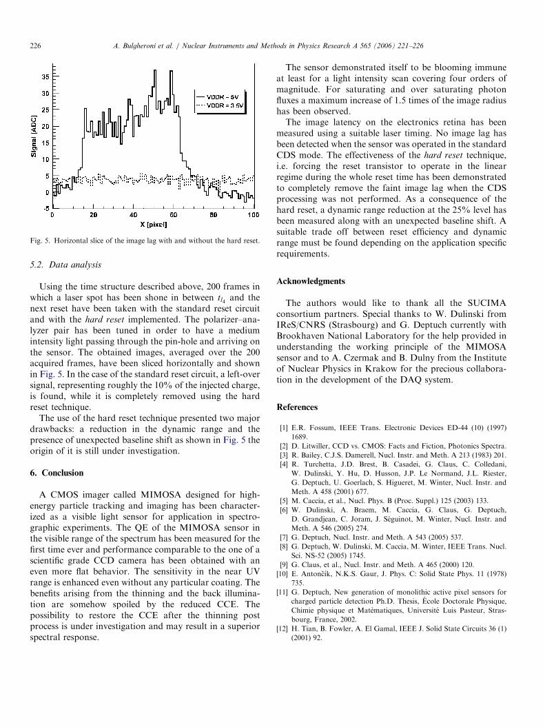
Fig. 5. Horizontal slice of the image lag with and without the hard reset.
A. Bulgheroni et al. / Nuclear Instruments and Methods in Physics Research A 565 (2006) 221–226226
5.2. Data analysis
Using the time structure described above, 200 frames inwhich a laser spot has been shone in between tl4 and thenext reset have been taken with the standard reset circuitand with the hard reset implemented. The polarizer–ana-lyzer pair has been tuned in order to have a mediumintensity light passing through the pin-hole and arriving onthe sensor. The obtained images, averaged over the 200acquired frames, have been sliced horizontally and shownin Fig. 5. In the case of the standard reset circuit, a left-oversignal, representing roughly the 10% of the injected charge,is found, while it is completely removed using the hardreset technique.
The use of the hard reset technique presented two majordrawbacks: a reduction in the dynamic range and thepresence of unexpected baseline shift as shown in Fig. 5 theorigin of it is still under investigation.
6. Conclusion
A CMOS imager called MIMOSA designed for high-energy particle tracking and imaging has been character-ized as a visible light sensor for application in spectro-graphic experiments. The QE of the MIMOSA sensor inthe visible range of the spectrum has been measured for thefirst time ever and performance comparable to the one of ascientific grade CCD camera has been obtained with aneven more flat behavior. The sensitivity in the near UVrange is enhanced even without any particular coating. Thebenefits arising from the thinning and the back illumina-tion are somehow spoiled by the reduced CCE. Thepossibility to restore the CCE after the thinning postprocess is under investigation and may result in a superiorspectral response.
The sensor demonstrated itself to be blooming immuneat least for a light intensity scan covering four orders ofmagnitude. For saturating and over saturating photonfluxes a maximum increase of 1.5 times of the image radiushas been observed.The image latency on the electronics retina has been
measured using a suitable laser timing. No image lag hasbeen detected when the sensor was operated in the standardCDS mode. The effectiveness of the hard reset technique,i.e. forcing the reset transistor to operate in the linearregime during the whole reset time has been demonstratedto completely remove the faint image lag when the CDSprocessing was not performed. As a consequence of thehard reset, a dynamic range reduction at the 25% level hasbeen measured along with an unexpected baseline shift. Asuitable trade off between reset efficiency and dynamicrange must be found depending on the application specificrequirements.
Acknowledgments
The authors would like to thank all the SUCIMAconsortium partners. Special thanks to W. Dulinski fromIReS/CNRS (Strasbourg) and G. Deptuch currently withBrookhaven National Laboratory for the help provided inunderstanding the working principle of the MIMOSAsensor and to A. Czermak and B. Dulny from the Instituteof Nuclear Physics in Krakow for the precious collabora-tion in the development of the DAQ system.
References
[1] E.R. Fossum, IEEE Trans. Electronic Devices ED-44 (10) (1997)
1689.
[2] D. Litwiller, CCD vs. CMOS: Facts and Fiction, Photonics Spectra.
[3] R. Bailey, C.J.S. Damerell, Nucl. Instr. and Meth. A 213 (1983) 201.
[4] R. Turchetta, J.D. Brest, B. Casadei, G. Claus, C. Colledani,
W. Dulinski, Y. Hu, D. Husson, J.P. Le Normand, J.L. Riester,
G. Deptuch, U. Goerlach, S. Higueret, M. Winter, Nucl. Instr. and
Meth. A 458 (2001) 677.
[5] M. Caccia, et al., Nucl. Phys. B (Proc. Suppl.) 125 (2003) 133.
[6] W. Dulinski, A. Braem, M. Caccia, G. Claus, G. Deptuch,
D. Grandjean, C. Joram, J. Seguinot, M. Winter, Nucl. Instr. and
Meth. A 546 (2005) 274.
[7] G. Deptuch, Nucl. Instr. and Meth. A 543 (2005) 537.
[8] G. Deptuch, W. Dulinski, M. Caccia, M. Winter, IEEE Trans. Nucl.
Sci. NS-52 (2005) 1745.
[9] G. Claus, et al., Nucl. Instr. and Meth. A 465 (2000) 120.
[10] E. Antoncık, N.K.S. Gaur, J. Phys. C: Solid State Phys. 11 (1978)
735.
[11] G. Deptuch, New generation of monolithic active pixel sensors for
charged particle detection Ph.D. Thesis, Ecole Doctorale Physique,
Chimie physique et Matematiques, Universite Luis Pasteur, Stras-
bourg, France, 2002.
[12] H. Tian, B. Fowler, A. El Gamal, IEEE J. Solid State Circuits 36 (1)
(2001) 92.