Embed Size (px)
Citation preview
CHARACTERIZATION OF MODIFIED ITO
ANODE SURFACES WITH
4-[(3-METHYLPHENYL)(PHENYL)
AMINO]BENZOIC ACID FOR OLED
APPLICATIONS
A Thesis submitted to
the Graduate School of Engineering and Sciences of
İzmir Institute of Technology
in Partial Fulfillment of the Requirements for the Degree of
MASTER OF SCIENCE
in Physics
by
Nesli YAĞMURCUKARDEŞ
July 2011
İZMİR

We approve the thesis of Nesli YAĞMURCUKARDEŞ
____________________________
Assoc. Prof. Dr. Salih OKUR
Supervisor
____________________________
Assist. Prof. Dr. Şerafettin DEMİÇ
Committee Member
____________________________
Assoc. Prof. Dr. Mehmet Salih DİNLEYİCİ
Committee Member
6 July 2011
___________________________ __________________________
Prof. Dr. Nejat BULUT Prof. Dr. Durmuş Ali DEMİR
Head of the Department of Physics Dean of the Graduate School of
Engineering and Sciences
ACKNOWLEDGEMENTS
Firstly, I would like to thank my supervisor, Dr. Salih OKUR for his
encouragement and support during my master thesis education. I also would like to
thank Dr. ġerafettin DEMĠÇ and his coworkers for their contribution to this thesis.
I am also thankful to all my friends in ĠYTE but especially Atike ĠNCE and Hale
SERT as they made department of physics a wonderful working environment for me.
Moreover, my special thanks go to my lab friends Hasan AYDIN, Ali Kemal
HAVARE and MaviĢe ġEKER because of their friendship and support whenever I need.
Mehmet YAĞMURCUKARDEġ, my husband is another person I would like to
thank while we overcome all difficulties together.
Last but not least, I want to thank to my family; my father, MemiĢ TEKGÜZEL,
my mother, Nesil TEKGÜZEL as they have always supported and encouraged me…
This research was supported by TUBITAK with 108T718 project number.

iv
ABSTRACT
CHARACTERIZATION OF MODIFIED ITO ANODE SURFACES
WITH 4-[(3-METHYLPHENYL)(PHENYL)AMINO]BENZOIC ACID
FOR OLED APPLICATIONS
This thesis focuses on to improve OLED characteristics of fabricated devices by
modifying the ITO (anode) surface using novel carboxylic acid based molecule 4-[(3-
methylphenyl)(phenyl)amino]benzoic acid (MPPBA). In this study, commercial ITO
substrates were used as anodes. To modify the ITO surface, etched ITO substrates were
kept in 1mM MPPBA-ethanol solution. As a hole transport layer (HTL), N,N′-bis(3-
methylphenyl)-N,N′-diphenylbenzidine (TPD) or N,N′-Di-[(1-naphthyl)-N,N′-
diphenyl]-1,1′-biphenyl)-4,4′-diamine (NPB) small molecules were deposited using an
organic evaporator system under the vacuum of 10-6
Torr. Finally, as a cathode contact
layer, aluminum thin film of 120 nm was deposited on top of the fabricated organic thin
film layers. The final structure of the devices was obtained as ITO /SAM (2nm) /HTL
(50nm) /Al (120nm). The current-voltage characteristics of devices of unmodified bare
ITO and MPPBA modified ITO substrates were analyzed by using the space charge
limited current approach and Thermionic Schottky Emission Models. Additionally,
surface characterizations of the SAM modified thin films were carried out using Quartz
Crystal Microbalance (QCM), Atomic Force Microscopy (AFM), Kelvin Probe Force
Microscopy (KPFM), X-ray Photoelectron Spectroscopy (XPS), Cyclic Voltammetry
(CV) and Ultraviolet-visible Absorption Spectroscopy (UV-Vis) techniques. The
obtained results reveal that the modification of the ITO surface with MPPBA molecules
reduces the barrier height difference between the Fermi level of the anode and HOMO
level of the HTL. Hence the hole injection increases while the turn-on voltage
decreases. As a result of this process OLED characteristics were improved by using the
MPPBA SAM molecules.

v
ÖZET
OLED UYGULAMALARINA YÖNELĠK 4-[(3-
METĠLFENĠL)(FENĠL)AMĠNO]BENZOĠK ASĠT ĠLE MODĠFĠYE
EDĠLMĠġ ĠTO ANOT YÜZEYLERĠNĠN KARAKTERĠZASYONU
Bu tez, yeni sentezlenmiĢ karboksilik asit temelli kendiliğinden organize tek
katman 4-[(3-metilfenil)(fenil)amino]benzoik asit (MPPBA) molekülü ile ITO yüzeyini
modifiye ederek üretilen OLED ürünlerinin özelliklerini iyileĢtirmek üzerine
odaklanmıĢtır. Bu çalıĢmada, temin edilen ITO altlıklar kısa devre oluĢumunu
engellemek için bir kenarlarından asitle kaldırılarak anot katmanı olarak kullanıldı.
Yüzey özelliklerini değiĢtirmek için, ITO’lar 1mM’ lık etanol çözücülü MPPBA
çözeltisi içinde belli sure tutuldu. Elektron boĢluğu iletim tabakası (HTL) olarak N,N′-
bis(3-metilfenil)-N,N′-difenilbenzidin TPD (ya da N,N′-Di-[(1-naftil)-N,N′-difenil]-
1,1′-bifenil)-4,4′-diamin NPB) küçük molekülleri organik buharlaĢtırma sistemi ile
yüksek vakum altında modifiye edilmiĢ ITO üzerine kaplandı. Katot tabakası olarak da
alüminyum elektrotlar metal buharlaĢtırma sistemi ile yine yüksek vakum altında
kaplandı. OluĢturulan OLED’lerin son yapıları ITO/KOT (2nm) /HTL (50nm) /Al
(120nm) Ģeklindedir. Yalın ve MPPBA molekülleriyle modifiye edilmiĢ ITO altlıklar
kullanılarak üretilen OLED aletlerin akım-voltaj karakteristikleri karĢılaĢtırmalı olarak
analiz edildi. Bunlara ek olarak, Kendiliğinden Organize Tek Katman (KOT)
moleküllerle modifiye edilmiĢ ince filmlerin yüzey karakterizasyonları Kuvars Kristalli
Mikro Terazi (QCM), Atomik Kuvvet Mikroskobu (AFM), Kelvin Milli Kuvvet
Mikroskobu (KPFM), X-ıĢını Fotoelektron Spektroskopisi (XPS), DönüĢümlü
Voltametre (CV) ve Ultraviyole-görünür Bölge IĢık Absorpsiyon Spektrofotometresi
(UV-Vis) teknikleri kullanılarak analiz edildi. Elde edilen sonuçlar KOT molekülerinin
varlığını doğrulamaktadır. ITO yüzeyinin MPPBA molekülleri ile modifiye edilmesi
anot Fermi düzeyi ile elektron boĢluğu iletim tabakası arasındaki bariyer yüksekliğini
azaltmakta ve bu sebeple elektron boĢluğu iletimini arttırırken çalıĢma voltajını
düĢürmektedir. Sonuç olarak, MPPBA KOT molekülleri kullanılarak OLED özellikleri
iyileĢtirilmiĢtir.

vi
To my Family

vii
TABLE OF CONTENTS
LIST OF FIGURES . .................................................................................................................... x
LIST OF TABLES.. .............................................................................................................. …xiv
CHAPTER 1. INTRODUCTION ................................................................................................. 1
1.1. Overview ............................................................................................................ 1
1.2. Research Objectives ........................................................................................... 2
1.3. Outline of Thesis ............................................................................................... 2
CHAPTER 2. ORGANIC LIGHT EMITTING DIODES ............................................................ 3
2.1. Advantages of OLEDs ........................................................................................ 3
2.2. History of Electroluminescence and OLED Technology ................................... 4
2.3. Organic Semiconductors and Organic Light Emitting Diodes ........................... 5
2.4. Basic OLED Device Structure ............................................................................ 8
2.5. OLED Device Operation .................................................................................. 10
2.5.1. Charge Injection and Transport .................................................................. 12
2.5.1.1. Schottky Injection and Fowler-Nordheim Tunneling ....................... 12
2.5.1.2. Space Charge Limited Current .......................................................... 15
2.5.1.3. Trap Charge Limited Current ............................................................ 17
2.5.1.4. The Role of Interfaces for Charge Injection ...................................... 17
2.5.2. Langevin Recombination ............................................................................ 20
2.5.2.1. Singletand Triplet Excited States ...................................................... 20
2.5.2.2. Light Emission .................................................................................. 22
2.5.3. OLED Efficiency and Light Outcoupling .................................................. 24
2.5.3.1. Efficiency .......................................................................................... 24
2.5.3.2. Light Outcoupling ............................................................................. 25
CHAPTER 3. SELF-ASSEMBLED MONOLAYERS .............................................................. 27
3.1. History of SAMs ............................................................................................... 27
3.2. Types of SAMs ................................................................................................. 28
3.3. SAM Formation ................................................................................................ 29

viii
3.4. SAM Characterization Techniques .................................................................. 31
3.4.1. Quartz Crystal Microbalance (QCM) ........................................................ 31
3.4.2. Atomic Force Microscopy (AFM) ............................................................ 34
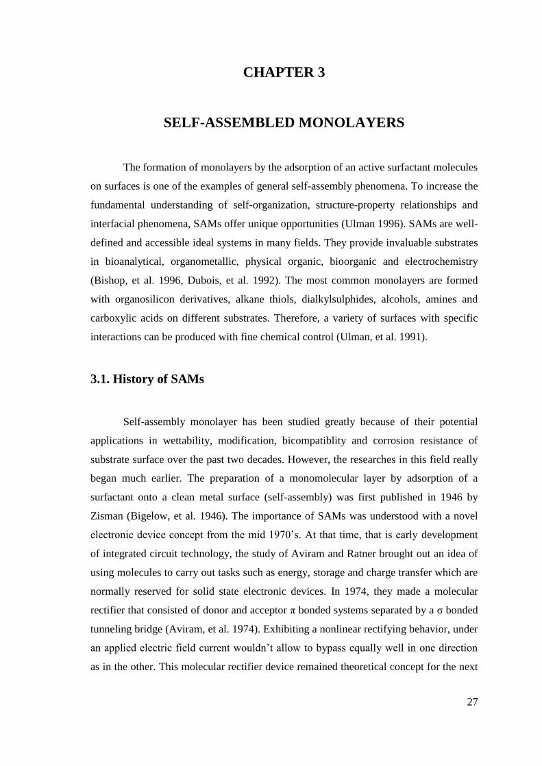
3.4.3. Kelvin Probe Microscopy (KPFM) ............................................................ 37
3.4.4. X-ray Photoelectron Spectroscopy (XPS) .................................................. 40
3.4.5. Cyclic Voltammetry (CV) .......................................................................... 41
3.4.6. Ultraviolet-visible Absorption Spectroscopy (UV-Vis) ............................. 43
3.5. SAM Applications ........................................................................................... 46
CHAPTER 4. EXPERIMENTAL DETAILS ............................................................................. 47
4.1. Chemical Compounds and Materials ................................................................ 47
4.2. Sample Preparation ........................................................................................... 49
4.2.1. ITO Coated Glass Substrate Preparation .................................................... 49
4.2.2. SAM Formation .......................................................................................... 50
4.2.3. Deposition of Organic Layers .................................................................... 50
4.2.4. Deposition of Cathode Layer ..................................................................... 51
4.3. Characterization ................................................................................................ 52
4.3.1. Adsorption Kinetics of SAM Molecules .................................................... 52
4.3.2. AFM Surface Characterization (Topography and KPFM) ......................... 53
4.3.3. X-Ray Photoelectron Spectroscopy (XPS) ................................................. 54
4.3.4. Cyclic Voltammetry (CV) .......................................................................... 55
4.3.5. Electrical Characterization (I-V) ................................................................ 55
CHAPTER 5. RESULTS AND DISCUSSION ......................................................................... 57
5.1. Surface Characterization Results ...................................................................... 57
5.1.1. Quartz Crystal Microbalance (QCM) Results ............................................ 57
5.1.2. Atomic Force Microscopy (AFM) Results for ThinFilms ......................... 60
5.1.3. Kelvin ProbeForce Microscopy (KPFM) Results for Thin
Films…………….………………………………………………………..66
5.1.4. X-Ray Photoelectron Spectroscopy (XPS) Results .................................... 69
5.1.5. Cyclic Voltammetry (CV) Results ............................................................. 72
5.1.6. Ultraviolet-visible Spectroscopy (UV-Vis) Results ................................... 73
5.2. Electrical Characterization Results of Organic Diodes .................................... 73

ix
5.2.1. Electrical Rectification Characteristics ..................................................... 73
5.2.1.1. Schottky Thermal Injection Results ................................................ 73
5.2.1.2. Space Charge Limited Current Results ........................................... 78
5.2.2. Current-Voltage Characteristics of OLEDs with SAM Modified ITO ...... 83
CHAPTER 6. CONCLUSION ................................................................................................... 87
REFERENCES ……. ................................................................................................................. 90

x
LIST OF FIGURES
Figure Page
Figure 2.1. Illustration of the (a) 2s-, (b) 2p- and (c) the hybrid orbitals for a
carbon atom. ................................................................................................... 6
Figure 2.2. The potential difference between the HOMO and LUMO levels.. .............. 7
Figure 2.3. Small molecules used in OLED fabrication ................................................. 9
Figure 2.4. Some Polymers used in OLED devices. ....................................................... 9
Figure 2.5. Basic structure of an organic light emitting diode (OLED) ....................... 11
Figure 2.6. Two injection mechanisms at the organic/metal interface (a) Schottky
carrier injection (b) Fowler-Nordheim tunneling……. ............................... 13
Figure 2.7. The schematic picture showing the energy level alignment at the
interface of an electrode and organic layer.. ................................................ 18
Figure 2.8. Schematic picture showing the energy level alignment at the interface
of an electrode and organic layer.. ............................................................... 19
Figure 2.9. Diagram showing possible singlet and triplet excitons formation ……….22
Figure 2.10. Jablonski diagram of electronic singlet and triplet states and possible
transitions between these states. .. ............................................................... 23
Figure 2.11. Bottom-emitting (left) and top-emitting (right) OLEDs. .. ........................ 26
Figure 3.1. Schematic representation of self-assembled monolayer and alkanethiol
molecule. ...................................................................................................... 29
Figure 3.2. A schematic representation of self-assembly of molecules by
immersing a substrate into a solution.. ......................................................... 30
Figure 3.3. A schematic diagram showing chemisorption reaction of a surfactant
on a substrate.. .............................................................................................. 31
Figure 3.4. Representation of basic principle of AFM and photodiode sections.......... 36
Figure 3.5. Interatomic force vs. distance curve. .......................................................... 37
Figure 3.6. Measurement Circuit of the tip-sample interaction in KPFM……............38
Figure 3.7. Schematic diagram of XPS system. ........................................................... 41
Figure 3.8. The Waveform Excitation Signal for Cyclic Voltammetry ........................ 42
Figure 3.9. Interband optical absorption process .......................................................... 44
Figure 3.10. The basic setup for measuring the absorption or transmission of light
through a sample. ....................................................................................... 44
Figure 3.11. The schematic of double beam UV-Visible spectrometer. ......................... 45

xi
Figure 4.1. Chemical structures of (a) Alq3, (b) TPD and (c) NPB.. ............................ 47
Figure 4.2. Schematic diagram of the synthesis process of MPPBA molecule. ........... 48
Figure 4.3. (a)A scheme of the plasma cleaning process and (b) a picture taken
during plasma cleaning process in our system.. ........................................... 49
Figure 4.4. The self-assembly process. ......................................................................... 50
Figure 4.5. Evaporation system for deposition of organic layers.. ............................... 51
Figure 4.6. (a) Outside and (b) inside photos of metal evaporation system. ................ 51
Figure 4.7. (a) The mask used in Al cathode deposition and (b) top view of the
final device structure. ................................................................................... 52
Figure 4.8. The Quartz Crystal Microbalance and peristaltic pump system. ................ 53
Figure 4.9. AFM and KPFM system............................................................................. 53
Figure 4.10. UIC Microphysics Lab XPS system. ......................................................... 53
Figure 4.11. The Current-Voltage Measurement Setup. ................................................ 56
Figure 5.1. Delta frequency vs. Time plot of fluidic MPPBA solution. ....................... 57
Figure 5.2. Mass change vs. Time plot with the formation of SAM monolayer. ......... 58
Figure 5.3. Delta frequency vs. Time plot of static MPPBA solution. ......................... 59
Figure 5.4. Mass change vs. Time plot of static MPPBA SAM solution. .................... 59
Figure 5.5. (a) Surface Topography and (b) Phase contrast image of bare ITO
surface .......................................................................................................... 60
Figure 5.6. (a) Surface Topography and (b) Phase contrast image of MPPBA
modified ITO surface.. ................................................................................. 61
Figure 5.7. (a) Surface Topography and (b) Phase contrast image of TPD coated
ITO surface .................................................................................................. 62
Figure 5.8. (a) Surface Topography and (b) Phase contrast image of MPPBA
modified/TPD coated ITO surface ............................................................... 63
Figure 5.9. (a) Surface Topography and (b) Phase contrast image of MPPBA
modified/TPD coated ITO surface. .............................................................. 64
Figure 5.10. (a) Surface Topography and (b) Phase contrast image of MPPBA
modified/NPB coated ITO surface ............................................................... 65
Figure 5.11. (a) Surface topography (b) Kelvin Probe Surface potential images of
bare ITO surface. ......................................................................................... 66
Figure 5.12. (a) Surface topography (b) Kelvin Probe Surface potential images of
MPPBA modified ITO surface. ................................................................... 67

xii
Figure 5.13. (a) Surface topography and (b) Kelvin Probe Surface potential images
of MPPBA modified/TPD coated ITO surface. ........................................... 67
Figure 5.14. (a) Surface topography and (b) Kelvin Probe Surface potential images
of MPPBA modified/NPB coated ITO surface. ........................................... 68
Figure 5.15. Kelvin Probe Surface Potential Current-Voltage Plot ................................ 68
Figure 5.16. XPS survey spectrum of MPPBA modified ITO surface. .......................... 70
Figure 5.17. XPS C 1s spectrum of MPPBA. ................................................................. 71
Figure 5.18. XPS O 1s spectrum of MPPBA…………………………………………...71
Figure 5.19. Cyclic voltammograms of the MPPBA (in solution) and MPPBA
coated on ITO surface .................................................................................. 72
Figure 5.20. UV spectrum of MPPBA coated ITO substrate ......................................... 73
Figure 5.21. I-V characteristics of fabricated ITO/Al, ITO/MPPBA/Al,
ITO/MPPBA/NPB/Al and ITO/NPB/Al devices.. ....................................... 74
Figure 5.22. I-V characteristics of fabricated ITO/Al, ITO/MPPBA/Al,
ITO/MPPBA/TPD/Al and ITO/TPD/Al devices. ........................................ 75
Figure 5.23. Current-Voltage behavior of bare n-type silicon and MPPBA modified
n-type silicon ............................................................................................... 76
Figure 5.24. The Current-Voltage behavior of bare p-type silicon and MPPBA
modified p-type silicon devices. .................................................................. 77
Figure 5.25. The Current-Voltage behavior ITO/NPB/Al between (-10)V and 10V. .... 78
Figure 5.26. The Current-Voltage behavior ITO/MPPBA/NPB/Al between (-10)V
and 10V region ............................................................................................. 79
Figure 5.27. The logarithm of J/E2 versus the square root of the applied electric
field for ITO/NPB/Al and ITO/MPPBA/NPB/Al devices ........................... 79
Figure 5.28. The carrier mobility of ITO/NPB/Al and ITO/MPPBA/NPB/Al
devices .......................................................................................................... 80
Figure 5.29. The Current-Voltage behavior ITO/TPD/Al between (-10)V and 10V. .... 81
Figure 5.30. The Current-Voltage behavior ITO/MPPBA/TPD/Al between (-10)V
and 10V region ............................................................................................ 81
Figure 5.31. The logarithm of J/E2 versus the square root of the applied electric
field for ITO/TPD/Al and ITO/MPPBA/TPD/Al devices. .......................... 82
Figure 5.32. The carrier mobility of ITO/TPD/Al and ITO/MPPBA/TPD/Al
devices. ......................................................................................................... 83

xiii
Figure 5.33. The Current density vs. Voltage Plot of devices fabricated with bare
ITO and MPPBA modified ITO substrates using NPB as HTL. ................. 84
Figure 5.34. The EL intensity spectrum of devices with bare ITO and MPPBA
modified ITO substrates using TPD as HTL ............................................... 84
Figure 5.35. The Current density vs. Voltage Plot of devices fabricated with bare
ITO and MPPBA modified ITO substrates using NPB as HTL. ................. 85
Figure 5.36. The EL intensity spectrum of devices with bare ITO and MPPBA
modified ITO substrates using NPB as HTL .............................................. 86

xiv
LIST OF TABLES
Table Page
Table 5.1. Roughness values of fabricated thin films ..................................................... 65
Table 5.2. Kelvin Probe Surface Potential values measured by KPFM Technique ....... 69
Table 5.3. Calculated ideality factor and barrier height values of devices with NPB
organic layer ................................................................................................... 75
Table 5.4. Calculated ideality factor and barrier height values of devices with TPD
organic layer ................................................................................................... 76
Table 5.5. The calculated ideality factor and barrier height values of bare and MPPBA
modified n-type and p-type silicon devices .................................................... 77

1
CHAPTER 1
INTRODUCTION
1.1. Overview
Organic optoelectronics has been an attractive field of research for almost two
decades. A novel electronic technology has been dedicated to organic electronics.
Conventional polymers, small molecules, plastics are now useful materials due to low
voltage operation enabling application properties for portable electronics. The discovery
and the development of conducting polymers by Alan Heeger, Alan MacDiarmid and
Hideki Shirakawa led to today’s device applications as active and passive electronics
and optoelectronics devices such as diodes, transistors, lasers, solar cells and
photodiodes.
The current display technologies such as Liquid Crystal Displays (LCD) and
Cathode Ray Tubes (CRTs) are underrated as OLEDs are flat panel displays with high
resolution using less energy. The advantages also include good self-luminance
efficiency without the use of backlight, wide viewing angle, high image content, low
temperature process and promise of full color. At the moment, passive monochrome and
active-matrix full color displays are commercially available.
The materials used in OLED fabrication have significant role in device
performance. Therefore, studies focused on the development and the improvement of
molecular materials. In addition, the charge injection and transport mechanisms have
great importance on operating voltage and luminance efficiency. In order to improve the
hole and electron injection, additional active thin layer was inserted. In order to
understand the OLED characteristics, there are several studies and developments in this
field.
In the near future, displays with various sizes, resolutions and purposes will be
found in all aspects of our daily lives. Billboards will be changed to dynamic posters,
flashy displays; wall paintings will be transformed to digital scenery and photographs.
Displays will be produced in many different shapes, forms and actually transparent.

2
1.2. Research Objectives
The objectives of this thesis are to reduce the barrier of hole injection and to
improve adhesion characteristic at the anode-organic film interface by the use of
benzoic acid derivative compound which have the ability to form self-assembled
monolayers (SAMs). SAM modified organic light-emitting devices (OLED) were
fabricated in the structure of multiple layer device. The current-voltage relations and the
electroluminescence of SAM modified OLEDs were characterized and compared with
unmodified devices. In addition, to investigate the surface properties, Quartz Crystal
Microbalance (QCM), Atomic Force Microscopy (AFM), Kelvin Probe Force
Microscopy (KPFM), X-ray Photoelectron Spectroscopy (XPS), Cyclic Voltammetry
(CV) and Ultraviolet-visible Spectroscopy (UV-Vis) characterization techniques were
used.
1.3. Outline of Thesis
There are six chapters in this thesis. In chapter two, the nature of the OLED,
device theory, material and device structure are explained. In chapter three, SAM
phenomenon, history of SAM applications, formation process and characterization
techniques have been discussed briefly. In chapter four, the device fabrication process is
presented. The surface characterization and the electrical characterization results of the
organic diodes are shown in chapter five, including its discussion. Finally, chapter six
constitutes the conclusion of this study.

3
CHAPTER 2
ORGANIC LIGHT EMITTING DIODES
Organic light- emitting diodes (OLEDs) as a novel device technology for flat
panel displays have received a great attention in the research community for the last two
decades. OLEDs consist of a thin fluorescent organic film sandwiched between two
electrodes (a transparent conducting anode and a metallic cathode). When external bias
voltage is applied to the conductive electrodes, charge carriers get injected into the
organic layer and recombination takes place in the bulk. As a result of this
recombination, visible, infrared and ultra-violet radiation can be produced.
Until now, OLED displays are used in the panel of a mobile phone, digital
camera, car audio, MP3 player and other portable small electronic applications. They
are unconventional and operate at low voltages, of the order of 3 - 5 V. Experimentally
OLEDs are already more efficient than incandescent lamps. It is expected that OLED
technologies will be able to take over earlier display industries after the fabrication of
flat panel displays with large scales are realized.
2.1. Advantages of OLEDs
Compared to other display technologies, OLEDs have many advantages. For
example, OLEDs have low operating voltage with high brightness. White OLEDs’
brightness can be up to 150,000 cd/m2. There is no need of backlight or filters as
OLEDs can emit light themselves. Therefore, OLEDs are lightweight devices with thin
displays like the newest prototypes of SONY displays measuring only 0.3 mm. There is
a wide range of organic materials to produce the fundamental colors (red, blue and
green). OLEDs are compatible with plastic substrates paving the way for flexible color
display technologies. Unlike liquid-crystal displays (LCDs), OLEDs have wide viewing
angle as high as 160 degrees. In addition, electroluminescence decay time of an OLED
is smaller than 1 μs.

4
Although OLED display technologies have many advantages, they have main
disadvantage such as the degradation of the materials by oxygen and water molecules
(Sugiyama, et al. 2000). As a result of this issue, operational lifetimes of OLEDs are
limited. However, by encapsulation, OLEDs lifetimes are now comparable with other
standard LEDs commercial products.
2.2. History of Electroluminescence and OLED Technology
Light emission occurs from an OLED device when external bias is applied
(Electroluminescence (EL)). In the early 1960s, Pope et al. (Pope, et al. 1963)
discovered organic electroluminescence from anthracene crystals. When high amount of
bias (V) was applied to these crystals with the thickness of μm to mm, light emission
occurred. As such voltages are not practical for most applications, up to 1980s therefore
the experimental results were postponed. Although Vincett et al. (Vincett, et al. 1982)
obtained EL from vacuum-deposited anthracene by applying voltages of only 30 V in
1982, these voltages were still not appropriate for applications.
The fundamental breakthrough was achieved in late 1980s, when C. W. Tang
and S. A. Van Slyke (Tang, et al. 1987) from Eastman Kodak demonstrated highly
efficient light emitting diodes by using organic small conjugated molecules as a
multilayer thin film. In the basic structure of the device N,N′-bis(3-methylphenyl)-N,N′-
diphenyl-4,4’ diamine (TPD) and tris(8-hydroxyquinoline) aluminum (Alq3) small
molecular weight organic materials were used as hole transport layer and electron
transport layer, respectively. Under less than 10 V bias, more than 1000 cd/m2
brightness and 1% external quantum efficiency (photons and electrons) were achieved.
Also, as a result of thin film structure (overall thickness ~100 nm), operating voltage
reduced and luminous efficiency increased significantly.
Later in 1990, Burroughs et al. introduced the first polymer based light emitting
diodes using poly(phenylenevinylene) (PPV) (Burroughes, et al. 1990). By spin coating
method, PPV thin film coated between two electrodes. When voltage was applied
between these electrodes, a yellow-green light was produced. In polymer based light
emitting diodes (PLED), quantum efficiency was only 0.05% as they do not have
heterojunction.

5
In general, in small molecular OLEDs and PLEDs, light emission is produced as
a result of fluorescent emission of singlet excitons. The carrier recombination can
produce singlet and triplet excitons in the ratio of 1:3. Although the singlet excitons
decay radiatively producing EL, triplet excitons decay non-radiatively. Therefore,
maximum value of EL efficiency is limited 25% by spin statistics. M. A. Baldo et al.
demonstrated that by introduction of phosphorescent dopants into OLED devices, the
energy from all the triplet states could be harnessed as phosphorescent light (Baldo, et
al. 1998). Therefore, the theoretical limit of molecular EL efficiency can reach up to
100%. In the recent experiments, green and red emitting phosphorescent OLEDs have
nearly 100% internal quantum efficiencies and 19% external quantum efficiencies.
The power efficiencies of OLED devices in different colors have been increased
and white OLEDs reach the efficiencies that are close to fluorescent lamps. It is
doubtful that OLED technologies will be able to take over the other display industry in a
little while.
2.3. Organic Semiconductors and Organic Light Emitting Diodes
The main difference between organic semiconductor and inorganic
semiconductor is that organic semiconductors contain carbon-based molecules that
interact through dipole-dipole forces. Almost all organic materials are insulators with
wide bandgaps and low conductivity (Abkowitz, et al. 1968, Almeleh, et al. 1966,
McGinnes, et al. 1974, Shirakawa, et al. 1977). However, in recent years, studies
showed that in organic-thin film devices, charge carrier mobilities exceeding
comparable values with mobilities in amorphous silicon (Haddock, et al. 2005, Kelley,
et al. 2004, Nelson, et al. 1998).
Organic semiconductors can also emit light in the visible region, as they have
band gaps in the range of 1.5 to 3.5 eV. They have vast potential to transform electronic
devices and save energy. In organic semiconductors, processing can be done at low
temperatures whereas in inorganic semiconductors high temperature is required.
To describe the chemical bonding mechanism between the atoms in organic
compounds, orbitals are used. The orbitals are the wave functions, that can be defined
by solving Schrödinger Equation and they describe the region where one or two
electrons can be found for an atom. In carbon, there are four valence orbitals that are

6
responsible for the formation of covalent bonds (2s, 2px, 2py, 2Pz). The hybrid orbitals
are assumed to be the new orbitals that originated with the superposition of the s-p
orbitals. There are three kinds of hybrid orbitals (sp1, sp
2, sp
3 where subscripts denote
the number of p-orbitals) (Haldi 2008). The illustration of the 2s-, 2p- and the hybrid
orbitals are shown in Figure 2.1.
Figure 2.1. Illustration of the (a) 2s-,(b) 2p- and (c) the hybrid orbitals for a
carbon atom (Source: (Oxtoby, et al. 2003)).
For the covalent single bond (σ bond) formation, the hybrid orbitals are
overlapped. However the double and the triple bonds which consist of one sigma bond
and one or two pi bonds, occur in systems with sp2 or sp hybridization, respectively.
The bonding energy is smaller in π-bonds than in σ-bonds as the spatial overlap
between the hybrid orbitals in σ-bonds is large, whereas the overlap of p-orbitals in π-
bonds is rather small. As a result of delocalization of electrons in p-orbitals due to the
weaker coupling, more polarization of electrons can be expected. In the conjugated
systems, the electron delocalization can be achieved over an even longer range of
distance than just two atoms since along the chain p-orbitals keep overlapping.
In a system with several atoms and electrons the Schrödinger equation becomes
very complicated. Therefore, by neglecting certain terms of Hamiltonian, eigenfunctions
and eigenvalues of the Hamiltonian can be approximated. The linear combination of

7
atomic orbitals-molecular orbitals (LCAO-MO) is one of these approximations for
molecular orbitals. Since the electrons in σ-bonds are harder to remove than electrons in
π-bonds, their contributions can be neglected (Pope, et al. 1999). Therefore, only π-
molecular orbitals will be focused.
The π-molecular orbital wavefunction ψπ can be defined in the first
approximation as linear combinations of the atomic p-orbitals with wavefunction Φl :
𝜓𝜋 = 𝑎𝑙𝛷𝑙𝑁𝑙=1 (2.1)
where N is the number of carbon atoms in the molecule, 𝑎𝑙 are linear coefficients, and
the sum goes over all carbon atoms (Pope et al. 1999). For N carbon atoms, orthogonal
N molecular orbitals in the given hermiticity of Hamiltonian can be defined. According
to Pauli-Exclusion Principle, in the ground state of a molecule, two electrons with
opposite spin fill the molecular orbitals with the lowest energies. The filled molecular
orbital of the highest energy is then called the highest occupied molecular orbital
(HOMO), whereas the molecular orbital with electron free next higher energy is called
the lowest unoccupied molecular orbital (LUMO). The potential difference between
HOMO and LUMO is called band gap that is determined by chemical structure of a
material and the delocalization of the π electrons. The electron affinity of the molecule
is correlated with the LUMO level. The HOMO level can be derived from the ionization
potential, as shown in Figure 2.2.
Figure 2.2. The potential difference between the HOMO and LUMO levels.
8
As the organic molecules of molecular solids are within close distance to each
other, molecular orbitals of different molecules overlap. Therefore, a system with two
molecules cannot be considered like two separate molecules, but because of the
interactions between the molecules the energy of the molecular orbitals splits. As the
number of the molecules that are interacting increases, the splitting energies cause a
bandlike structure that is compatible with valence band and conduction band in
inorganic semiconductors.
2.4. Basic OLED Device Structure
The main difference between LCD and OLED display is that OLED can emit
light by themselves. Therefore, the materials for OLED must have the capability to
inject charge from electrode, transport charge and finally emit fluorescence efficiently.
In addition to determining the color, emitting layer materials also influence the
efficiency of the devices. There are abundant organic materials to improve the device
performance and to emit different colored devices.
According to their molecular weight, the materials used for OLED fabrication
can be categorized into two classes; small molecules and polymers. Although organic
small molecules contain only a few carbon atoms, polymers consist of a long chain of
repeated units that are connected with covalent bonds.
Small molecular compounds can be deposited using thermal evaporation method
under high vacuum. To improve the charge injection and recombination and thus the
efficiency of the device, small molecules are fabricated as multi-layered structure. Some
common small molecules used in OLED devices shown in Figure 2.3.

9
Figure 2.3. Small molecules used in OLED fabrication.
Polymers, shown in Figure 2.4., as they are solution-coatable, can be deposited
using spin coating, dip coating or ink-jet printing methods. Due to the delocalized π-
molecular orbitals along the polymeric chain, polymers have a property of
semiconductors. Poly(p-phenylene-vinylene) (PPV) is the most used polymer in OLED
fabrication and its derivatives have good performance in light emitting efficiency.
Figure 2.4. Some Polymers used in OLED devices.
10
2.5. OLED Device Operation
Small molecular OLEDs are typically fabricated on transparent conducting
anode coated glass or flexible substrates. Due to its high work function and high
transparency (90%) to visible light, most OLEDs use ITO as the anode (Wang, et al.
1996). The most extensively used technique for ITO deposition is sputtering. Thermal
evaporation is the closely other used technique. Used deposition technique affects the
quality and reproducibility of the film, homogeneity over a wide cross-section, ease and
cost of use are the factors. The direct optical bandgap values of ITO films have been
reported as in the range of 3.5 to 4.06 eV (Balasubramanian, et al. 1989, Fan, et al.
1977, Haitjema, et al. 1991, Higuch, et al. 1994, Sreenivas, et al. 1985, Szczyrbowski, et
al. 1983). This wide bandgap semiconductor property of ITO films gives the high
optical transmittance, Tr. The transparency and conductance is directly related with the
film thickness and composition ratio of two components. The resistivity of a 200nm
thick ITO is about 10-3
Ω.cm with mobility (μ) near to 10 cm2/Vs. Also the reported
refractive index value for ITO is 1.96 (Szczyrbowski et al. 1983). For the efficient hole
injection, high work function (Φ0) is needed as the HOMO level energies of the organic
materials are typically 5-6 eV. According to applied surface treatment, the work
function of ITO varies between 4.1 and 5.1 eV (Hosokawa, et al. 1995, Li, et al. 1997b,
Milliron, et al. 2000, Nüesch, et al. 2000). Ultraviolet photoelectron spectroscopy (UPS)
and X-ray photoelectron spectroscopy (XPS) studies have shown that surface treatment
cause a generated dipole layer and modified electronic structure is therefore changed Φ0
(He, et al. 2001, Hosokawa et al. 1995, Ishii, et al. 1999, Milliron et al. 2000, Nüesch et
al. 2000, Sugiyama et al. 2000). For the reduction of the energy barrier height for hole
injection, the vacuum level of ITO/organic interface is changed by the surface dipole
layer (Ishii et al. 1999).
As a cathode layer, materials must have properties such as high conductivity,
low work function to promote electron injection from Fermi level of the cathode to the
LUMO level of organic material, good stability and film-forming. Ca (Φ0 ~ 3 eV), Mg
(Φ0 ~ 3.7 eV) and Al (Φ0 ~ 4.3 eV), are the low work function materials that are used as
cathode layer. As the low work function metals react with oxygen and water molecules
easily, additional insulating layer such as LiF, CsF or AlOx can be inserted to protect
device from degradation and thus, reduce the barrier for electron injection (Aziz, et al.

11
1998, Brown, et al. 2001, Brown, et al. 1999, Brütting, et al. 2001, Burrows, et al. 2000,
Jabbour, et al. 1998, Li, et al. 1997a, Piromreun, et al. 2000, Suzuki 1996, Turak, et al.
2002).
The basic device structure of multilayered OLED, as shown in Figure 2.5.,
consists of an anode, a cathode, a hole transport layer (HTL) and an electron transport
layer (ETL).
Figure 2.5. Basic structure of an OLED.
When the applied bias Vapp is less than the built in voltage Vbi, most of the
current is generated by free carriers of organic layer or leakage current therefore the
injected current is small and negligible. At high applied forward voltage to the
electrodes, electrons from cathode are injected into the LUMO level of the ETL and
holes injected from the anode into the adjacent HTL. If the density of the electrons and
holes are sufficiently high, the distance becomes closer and carriers travel toward the
junction of the ETL and HTL where they recombine and emit light. Since the number of
electrons injected is not equal to the number of holes, there is a charge imbalance which
minimizes the efficiency of the device (Shinar 2004).
Working phenomenon of OLEDs is similar to that of an inorganic light emitting
diode as the emission of light takes place at the interface of p-type and n-type
semiconductor materials. In OLEDs light emission takes place near the interface of the

12
electron transport and hole transport layer. Injection of charge carriers from the metal
electrodes into the organic layers, transport of charge carriers in the organic layers and
recombination of charge carriers at the organic interfaces and formation of excitons are
the important processes that are involved in OLEDs for the light emission (Scott, et al.
2000). These processes are discussed in literature to understand the mechanism of light
emission in OLEDs.
2.5.1. Charge Injection and Transport
Under the conditions of a low electric field (<104 V/cm), all of the organic
molecular materials used for OLED devices electrically behave as an insulator. As the
vacuum sublimed organic films have the resistivity in the order of 1015
Ω-cm, without
chemical doping no net charge carriers can be present in purified organic materials
intrinsically. However, very high current density up to 1A/cm2 in OLED can be
obtained in operation. For the explanation of the high current densities new mechanisms
were introduced: carrier injection at electrode/organic interface, space charge limited
current (SCLC) and trap charge limited current (TCLC). Carrier injection at an
electrode/organic interface and SCLC, large current density is provided. As mentioned
before, electronic structure of OLED based on the individual molecules located at
HOMO and LUMO levels of organic thin film. To form narrow conduction and valence
bands, each molecule interacts with Van der Walls forces. The intrinsic carrier densities
of organic semiconductors based on impurities and irregular structures of thin films are
very low (~ 103-10
5/cm
3). Also, charge mobility in organic semiconductors is smaller
than that in inorganic materials (μorganic~ 10-3
-10-7
cm2/V-s, μinorganic~ 1-10
3cm
2/V-s.
Carriers are injected into organic layer via Schottky thermal injection and Fowler-
Nordheim tunneling injection.
2.5.1.1. Schottky Injection and Fowler-Nordheim Tunneling
When the energy barrier is too high at the organic/electrode interface to generate
any high current density, through the localized levels, Schottky thermal injection is
induced by structural defects or unexpected impurities. When a contact between the

13
electrode and the organic layer is established, due to Coulomb attraction between the
injected electrons and left holes in the metal, the image force potential is formed. This
image potential lowers the energy of the interface states and makes them energetically
available for the electron hopping from the metal Fermi surface. Unfortunately, with
increasing distance from the interface decreases the image force potential and thus bulk
states deep in organic layer remain energetically unavailable for charge hopping. As a
result of applied external electric field the energy of the available states in the bulk
lowers and thus hopping into bulk states away from the interface becomes possible
(Singh 2009).
In the Fowler-Nordheim tunneling injection, hopping into the energetically
available state in the bulk occur with the penetration of electrons located on the metal
Fermi state through the thin triangular energy barrier. The two injection mechanisms
are illustrated below in Figure 2.6. (a) the Schottky carrier injection and (b) Fowler-
Nordheim Tunneling.
Figure 2.6. Two injection mechanisms at the organic/metal interface (a) Schottky carrier
injection (b) Fowler-Nordheim tunneling.

14
In Schottky injection mechanism when adequate thermal energy needed to cross
the barrier height is acquired, electrons from the metal electrode can be injected. The
process can be described by the equation (Scott 2003)
𝐽 = 4𝜋𝑞𝑚𝑘
3 𝑇2𝑒𝑥𝑝
−𝑞𝛷𝐵𝑛
𝑘𝑇 𝑒𝑥𝑝
𝑞𝑉
𝑘𝑇 − 1 (2.2)
where q is the electron charge, m is the effective mass of the electron or hole, k is the
Boltzmann’s constant, h is the Planck’s constant, T is the temperature, ΦBn is the barrier
height and V is the applied voltage.
The current-voltage characteristics for q(V-Rs) > kT values of the diodes can be
analyzed by the relation (Rhoderick, et al. 1988, Sze 1981);
𝐼 = 𝐼0𝑒𝑥𝑝 𝑞(𝑉 − 𝐼𝑅𝑠)
𝑛𝑘𝑇 1 − 𝑒𝑥𝑝 −
𝑞(𝑉 − 𝐼𝑅𝑠𝑘𝑇
(2.3)
where is the I0 saturation current and expressed as:
𝐼0 = 𝐴𝐴∗𝑇2𝑒𝑥𝑝 −𝑞∅𝐵𝑘𝑇
(2.4)
where Rs is the series resistance, q is the electron charge; V is the applied voltage; A∗
is the effective Richardson constant; A is the effective contact area; T is the absolute
temperature; k is the Boltzmann constant; n is the ideality factor; ∅B is the barrier
height. The saturation current obtained from the linear portion intercept of log I at zero
voltage.
The ideality factor and barrier height values of the four diodes were calculated
from the slope of the linear region and y-axis intercept of the forward bias ln(I)-V curve.
The obtained ideality factors that higher than unity indicates that diodes show non-ideal
behavior because of the interface layer and series resistance. This significant series
resistance effect can be analyzed by Cheung’s functions (Cheung, et al. 1986):

15
𝑑𝑉
𝑑 𝑙𝑛(𝐼)= 𝑛
𝑘𝑇
𝑞+ 𝐼𝑅𝑠 (2.5)
and a H(I)function can be defined as follows
𝐻 𝐼 = 𝑉 − 𝑛𝑘𝑇
𝑞𝑙𝑛
𝐼0𝐴𝐴∗𝑇2
= 𝐼𝑅𝑠 + 𝑛𝜙𝐵 (2.6)
For the Fowler-Nordheim tunneling injection, the current flow can be described
by the following equation (Scott 2003):
𝐽 = 𝑞3𝑉2𝑚0
8𝜋𝛷𝐵𝑛𝑚∗ 𝑒𝑥𝑝
−4(2𝑚∗)0.5𝛷𝐵𝑛1.5
3𝑞𝑉 (2.7)
where J is the current density, V is the voltage, h is the Planck’s constant, m0 is the mass
of the free electron, q is the charge of the electron, m* is the effective mass.
The charge injection process in OLEDs is described as a combination of these
two injection mechanisms. It is described by J.C. Scott as a thermally assisted tunneling
injection from the delocalized states of the metal to the localized organic layer (Scott
2003). The I-V characteristics of the OLEDs are due to these charge injection effects.
2.5.1.2. Space Charge Limited Current
If the applied electric field is less than 104 V/cm, the number of the charge
carriers injected into the organic layer is less than the intrinsic charge carriers present in
the organic layer and thus the current flow is governed by Ohm’s law. Charge
accumulations that were caused by charge injection into low mobility organic materials,
partially screen out by the applied electric field. With the high external electric field
(>105 V/cm), due to low carrier mobility, near the electrode/organic interface the
injected current density is higher than the intrinsic charge density therefore the internal
electric is enhanced by the space charges (Singh 2009). This type of current regime is
called as space charge limited current (SCLC) and given by the Mott-Gurney equation
(Mott, et al. 1940)

16
𝐽 = 9𝜀𝜀0𝜇𝑉
2
8𝐿3 2.8
where 𝜀 is the relative dielectric constant, 𝜀0 is the dielectric constant and 𝐿 is the
sample thickness and 𝜇 is the field independent charge carrier mobility. In the absence
of traps or a single shallow trap level, current-voltage curves predicted by this model are
supralinear. In OLEDs, the transport and the injection properties are determined by inter
site hopping from delocalized states in the metal to localized states in the organic layer.
The transition rate depends on the energy difference and distance between one site to
another. Narrow bands around the HOMO and LUMO levels are formed by the energy
states that are involved in the hopping transport of holes and electrons. The
intermolecular interactions and level of disorder determine the widths of these bands.
To improve the conduction in device where strong injection is achieved from both
electrodes, the SCLC type mechanisms are needed. When an external electric field is
applied, the holes are injected from anode into the HTL and drift or hope across it. Due
to low hole mobility in the electron transport layer ETL, holes decelerate at the internal
interface. According to Haichaun Mu, the same mechanism is also valid for electrons as
they cross organic/organic interface, which leads to substantial charge accumulation at
the interface (Mu 2011). The dependence of mobilities on electric field is best described
by the Poole-Frenkel type of behavior given by the following equation (Blom, et al.
1998):
𝜇 = 𝜇0𝑒𝑥𝑝 −∆
𝑘𝑇 𝑒𝑥𝑝 𝛾 𝐸 (2.9)
where ∆ is the activation energy, 𝜇0 is the temperature independent prefactor, 𝑘 is the
Boltzmann’s constant and 𝑇 is the temperature and 𝐸 is the applied electric field to the
terminals of the device. In the above equation, 𝜇 is directly proportional to 𝐸 which
points out the electric field dependence on mobility.

17
2.5.1.3. Trap Charge Limited Current
Besides being localized to individual molecules, charges can also accumulate in
traps, typically at organic layer interfaces or at defects within the film. Due to the strong
injection, the local increase in the quasi-Fermi level may lead to charge immobilization
in the deeper states of the disorder induced distribution of HOMO and LUMO levels. In
the presence of the traps, when forward bias is increased, the electron quasi-Fermi level
arises towards the LUMO with increasing injected electron density. If the traps are
distributed in energy, they will gradually fill with increasing field and the current will
increase faster than quadratic in SCLC until traps are filled (Singh 2009). This model is
called trap charge limited current (TCLC), in which a high power dependence of current
on voltage is observed. The trap density of the states is well described using an
exponential distribution of traps using the equation;
𝑁𝑡 𝐸 =𝑁𝑡𝑘𝑇𝑡
𝑒𝑥𝑝 𝐸 − 𝐸𝐿𝑈𝑀𝑂
𝑘𝑇𝑡 (2.10)
where 𝑁𝑡 is the total trap density, 𝑘 is the Boltzmann’s constant and 𝑇𝑡 is the
characteristic temperature of the exponential trap distribution (Tt=Et / k, where Et is the
characteristic trap energy). Therefore, below the quasi-Fermi level in the high injection
currents, the filling of traps controlled by the density and energy distribution of the
traps. The current density is also described by the equation;
𝐽𝑇𝐶𝐿 =𝑉𝑚+1
𝑑2𝑚+1 (2.11)
where 𝑚 = 𝑇𝑡 𝑇 .
2.5.1.4. The Role of Interfaces for Charge Injection
There are two main reasons for electronic level misalignments at the interfaces
which lead to the contact-limited injection regime: One of them is the mismatch of work

18
functions of electrode and electron affinity of the material in the device as shown in
Figure 2.7. Another one is the presence of additional barriers between organic layers.
Figure 2.7. The schematic picture showing the energy level alignment at the interface of
an electrode and organic layer. In these cases vacuum level alignment is
assumed.
In both cases presented in Figure 2.7., vacuum level is assumed as the reference.
The work function Φ of the anode and the cathode is the position of Fermi level to
vacuum level. Photoelectron spectroscopy is used as to characterize technique to obtain
work function and threshold ionization potential of a molecule and thus the hole
injection barrier can be estimated (Singh 2009).
The assumption of common vacuum level is not easy when inorganic electrode
and organic materials are involved. In literature, it is investigated that the interfacial
dipole is formed due to the formation of chemical bonds or charge transfer, and
manifests itself as a vacuum level offset (denoted as Δ) (Blochwitz, et al. 2001, Chkoda,
et al. 2000, Crispin, et al. 2002, Giebeler, et al. 1999, Ishii, et al. 2000, Ishii et al. 1999,
Kera, et al. 2004, Mäkinen, et al. 2001, Osikowicz, et al. 2004, Peisert, et al. 2004,
Salaneck, et al. 1996). Such offset influence on the magnitude of the barrier is shown in
Figure 2.8.

19
Figure 2.8. Schematic picture showing the energy level alignment at the interface of an
electrode and organic layer. In these cases vacuum level shift is present,
which increases injection barriers.
When the work function of the substrate (Φs) equals to the ionization potential
(IP) or to the electron affinity (EA) of the organic material, as a result of vacuum level
shift there is still a barrier at the interfaces. The existence of this barrier at the interface
influences the device characteristics. The large magnitude of barrier height causes
smaller injection current at a given voltage and to achieve the desired intensity of light
higher applied voltage is required.
The studies are still focused on the understanding and controlling the energy
level alignment at the interfaces. ITO is the most used electrode at anode in OLEDs. As
it is investigated in the study of Chkoda et al., although it has high work function, it has
lower ionization potential than most of the HTL materials (Chkoda, et al. 2000).
Besides studying on HTL materials, in order to provide the best match, also by
modifying the ITO surface, the work function can be significantly increased (Besbes, et
al. 2003, Ganzorig, et al. 2001, Hatton, et al. 2001, Ho, et al. 1998, Sugiyama, et al.
2000, Sun, et al. 2003, Wu, et al. 1997). The interfacial dipole is formed, when the work
function exceeds the energy of integer charge transfer state (ICTS). While hole injection
barriers remain constant, the magnitude of the dipole increases linearly with the work
function of the substrate.

20
2.5.2. Langevin Recombination
The light emission from an OLED device fundamentally is generated by
recombination occurred between injected hole and electron that forms various excited
states such as singlet excitons, triplet excitons and charge transfer excitons. When the
electric field is applied to the terminals of the OLED, both holes and electrons are
injected into organic layer and two carriers start interacting. The recombination of
statically independent oppositely charged carriers were first studied by Paul Langevin in
1903 (Langevin 1903). The desired condition for recombination is that the distance
between the hole and the electron must be less than the Coulomb capture or Onsager
radius, 𝑟𝑐 . Onsager radius is the distance, where the Coulomb attractive potential energy
equals to thermal dissociation energy (Zou, et al. 2001),
𝑟𝑐 =𝑞2
4𝜋𝜀𝑘𝑇 (2.12)
As 𝜀~3𝜀0 for most organic materials, at room temperature typical columbic
capture radius is ~17 nm (Swenberg, et al. 1999). The bimolecular recombination
current in the Langevin model is given by
𝑅 = 𝛾𝑛𝑒𝑝𝑒 =𝑒(𝜇𝑛𝜇𝑝)
𝜀𝑛𝑒𝑝𝑒 (2.13)
where 𝜇𝑛 , 𝜇𝑝 are the mobilities of negative and positive charegs and 𝑛𝑒 ,𝑝𝑒 are the
densities of the charge carriers and 𝛾 is the Langevin recombination coefficient.
2.5.2.1. Singlet and Triplet Excited States
In quantum mechanics, when one electron is excited from an occupied state into
an unoccupied state it leaves a hole. A hole represents just a missing electron, it can be
represented by similar wavefunctions with electron. According to Pauli Principle in a
system with two particles of spin 1/2, eigenstates of the Hamiltonian must be
antisymmetric with respect to the exchange of particles (Griffiths 2005). As long as the

21
spatial wavefunction has the opposite parity, the spin wavefunction can be either
symmetric or antisymmetric since wave functions can be written as the product of the
spatial and the spin wavefunctions. For the electron, the spin part of the wavefunction
can be represented by ∣↑⟩ or ∣↓⟩ where arrows indicate the direction of the spin.
Therefore, the four possible spin wavefunctions can be differentiated between one
antisymmetric (singlet) state Sn:
𝛹𝑠𝑝𝑖𝑛 =1
2 ∣↑⟩ ∣↓⟩−∣↓⟩ ∣↑⟩ (2.14)
and three antisymmetric (triplet) states Tn:
𝛹𝑠𝑝𝑖𝑛 =1
2 ∣↑⟩ ∣↓⟩+∣↓⟩ ∣↑⟩ (2.15)
𝛹𝑠𝑝𝑖𝑛 =∣↑⟩ ∣↑⟩ (2.16)
𝛹𝑠𝑝𝑖𝑛 =∣↓⟩ ∣↓⟩ (2.17)
Emission of light results in the transition of singlet excitons from a single state
to the ground state fast and efficiently. This is a fast and efficient radiative decay
because it does not involve in spin. Transition of triplet excitons from the triple state to
the ground state that involves spin flip. As a result of long transition time energy of
excitons is lost in the form of phonons. Figure 2.9. shows the four possible exciton
formations with one singlet formation and three triplet formations.
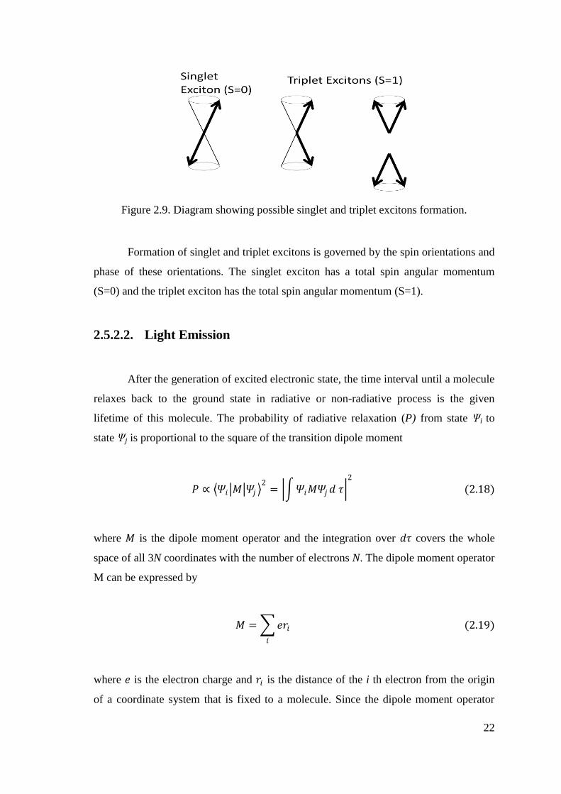
22
Figure 2.9. Diagram showing possible singlet and triplet excitons formation.
Formation of singlet and triplet excitons is governed by the spin orientations and
phase of these orientations. The singlet exciton has a total spin angular momentum
(S=0) and the triplet exciton has the total spin angular momentum (S=1).
2.5.2.2. Light Emission
After the generation of excited electronic state, the time interval until a molecule
relaxes back to the ground state in radiative or non-radiative process is the given
lifetime of this molecule. The probability of radiative relaxation (P) from state Ψi to
state Ψj is proportional to the square of the transition dipole moment
𝑃 ∝ 𝛹𝑖 𝑀 𝛹𝑗 2
= 𝛹𝑖𝑀𝛹𝑗𝑑 𝜏 2
(2.18)
where 𝑀 is the dipole moment operator and the integration over 𝑑𝜏 covers the whole
space of all 3N coordinates with the number of electrons N. The dipole moment operator
M can be expressed by
𝑀 = 𝑒𝑟𝑖𝑖
(2.19)
where 𝑒 is the electron charge and 𝑟𝑖 is the distance of the i th electron from the origin
of a coordinate system that is fixed to a molecule. Since the dipole moment operator

23
does not affect the spin part of the wavefunction of a state, only similar spin symmetry
transitions result in transition dipole moment that is different from zero. Having
absorbed energy and reached one of the higher levels of an excited state, molecule
rapidly loses its excess amount of energy by collisions and falls to the lowest singlet
excited state (S1). Light emission is generated with the return of electron to the various
levels of the ground singlet state (S0). The resulting radiation from such transitions is
called fluorescence.
Phosphorescence emission is the photon emission caused by the transition of the
molecule from lowest triplet excited state to (T1) to the ground state (S0). In addition to
the phosphorescence, both singlet and triplet character of the excited states in spin-orbit
coupling is also possible for transitions between the lowest excited singlet state S1 and
the lowest triplet excited state T1, the so-called intersystem crossing (ISC). According to
Hund’s rule the energy of T1 is generally lower than the energy of S1. Therefore, it is
more useful for an excited singlet state to relax to the ground state through intersystem
crossing to the triplet state that is phosphorescent emission instead of a fluorescent
relaxation (Haldi 2008). A Jablonski diagram of the radiative and non-radiative
transitions is shown in Figure 2.10.
Figure 2.10. Jablonski diagram of electronic singlet and triplet states and possible
transitions between these states.
In the figure, solid arrows represent radiative transitions, curvy lines show non-
radiative transition from higher excited states to the lowest excited state (internal
24
conversions, IC) and nonradiative transition from the lowest singlet to the lowest triple
state (intersystem crossing, ISC).
2.5.3. OLED Efficiency and Light Outcoupling
2.5.3.1. Efficiency
The most often reported performance quality of the OLED is its external
quantum efficiency (EQE). EQE is defined as the number of photons released from the
device per number of injected hole-electron pairs. The product of the internal quantum
efficiency ηint (number of photons generated inside the device per number of injected
hole-electron pairs) times the outcoupling efficiency (ηph) gives the external quantum
efficiency (ηext) (Adachi, et al. 2001):
𝜂𝑒𝑥𝑡 = 𝜂𝑖𝑛𝑡 𝜂𝑝 (2.20)
where the internal quantum efficiency is dependent on the device architecture and the
material properties of the device:
𝜂𝑖𝑛𝑡 = 𝛾𝜂𝑒𝑥𝛷𝑝 (2.21)
where 𝛾 is the electron-hole charge-balance or Langevin recombination factor, 𝜂𝑒𝑥 is
the efficiency of the formation of excited electronic states that lead to radiative
transitions, and 𝛷𝑝 is the photoluminescence quantum yield.
The photoluminescence quantum yield (𝛷𝑝) is a material constant that is
described by the number of radiative transitions per the number of total transitions from
the excited states to the ground state in a material. 𝜂𝑒𝑥 is also dependent on the material
that is given by the nature of the emission. As it is mentioned before, in fluorescent
devices radiative transitions occur only from the singlet excited state; therefore, 𝜂𝑒𝑥 can
only reach 25% upper limit since only one out of the four excited states is a singlet state
in small molecules (Baldo, et al. 1999). On the other hand, in polymers with longer

25
chain length attribute to a faster decay of higher excited states in compounds and thus
𝜂𝑒𝑥 can exceed the limit of singlet excited states up to 60% (Beljonne, et al. 2004,
Meulenkamp, et al. 2004).
In phosphorescent devices, all three triplet excited states participate in the light
emission. With the relaxation of high energy singlet excited state into the triplet state
through intersystem crossing, 𝜂𝑒𝑥 with 100% can be achieved (Adachi et al. 2001).
2.5.3.2. Light Outcoupling
General structure of OLEDs consists of ITO coated glass substrate that acts as a
transparent and conductive electrode, organic layer deposited and finally metal cathode.
As the light is extracted through the glass substrate, such devices are usually referred to
as bottom-emitting OLEDs as it is shown in Figure 2.11. However, this device
architecture is not very efficient in coupling out the emitted light through the substrate
and the into the viewer’s eye.
An estimated maximum light output of the bottom-emission geometry can be
calculated using simple ray theory assuming that the cathode acts as a perfect mirror.
The amount of light energy transmitted from a medium 1 with refractive index 𝑛1 into a
medium 2 with refractive index 𝑛2 normalized by light energy incident on the interface
between medium 1 and 2 is given by (He, et al. 2004, Kim, et al. 2000):
𝜂𝑝 = 1 − 1 − 𝑛2
𝑛1
2
≈ 0.5 𝑛2
𝑛1
2
(2.22)
As long as there is no local minimum of the refractive index within the
multilayer structure, this equation holds even for multilayer structures (Gu, et al. 1997).
In literature, there have been studies on improving the outcoupling efficiency. Most of
the researchers focus on treating the emitting surface of the glass substrate to avoid
internal total reflection between glass and air (Krummacher, et al. 2006, Madigan, et al.
2000). Additionally, to avoid waveguiding effects from ITO to glass interface is
modified (Agrawal, et al. 2007, Tsutsui, et al. 2001). However, basic bottom-emitting
OLEDs have the same intensity independent of the observer’s angle (Lambertian

26
emitter), improvements mostly occur mostly in the direction perpendicular to the glass
substrate which is typically not Lambertian (Agrawal et al. 2007).
Figure 2.11. Bottom-emitting (left) and top-emitting (right) OLEDs. Arrows in the
bottom-emitting OLED represent light that is waveguided in the ITO or
in the glass.
Alternatively, top-emitting OLEDs have been studied to avoid wave guiding
effects in the ITO layer and the glass substrates (Dobbertin, et al. 2003, Riel, et al.
2003). While the top electrode is transparent, top-emitting OLEDs are fabricated on
metal coated substrate that fully reflect the light. However, as a result of surface
Plasmon-polariton modes that occur at metal surfaces, the external quantum efficiency
can only reach about 20 to 25% (Huang, et al. 2006, Smith, et al. 2004).
27
CHAPTER 3
SELF-ASSEMBLED MONOLAYERS
The formation of monolayers by the adsorption of an active surfactant molecules
on surfaces is one of the examples of general self-assembly phenomena. To increase the
fundamental understanding of self-organization, structure-property relationships and
interfacial phenomena, SAMs offer unique opportunities (Ulman 1996). SAMs are well-
defined and accessible ideal systems in many fields. They provide invaluable substrates
in bioanalytical, organometallic, physical organic, bioorganic and electrochemistry
(Bishop, et al. 1996, Dubois, et al. 1992). The most common monolayers are formed
with organosilicon derivatives, alkane thiols, dialkylsulphides, alcohols, amines and
carboxylic acids on different substrates. Therefore, a variety of surfaces with specific
interactions can be produced with fine chemical control (Ulman, et al. 1991).
3.1. History of SAMs
Self-assembly monolayer has been studied greatly because of their potential
applications in wettability, modification, bicompatiblity and corrosion resistance of
substrate surface over the past two decades. However, the researches in this field really
began much earlier. The preparation of a monomolecular layer by adsorption of a
surfactant onto a clean metal surface (self-assembly) was first published in 1946 by
Zisman (Bigelow, et al. 1946). The importance of SAMs was understood with a novel
electronic device concept from the mid 1970’s. At that time, that is early development
of integrated circuit technology, the study of Aviram and Ratner brought out an idea of
using molecules to carry out tasks such as energy, storage and charge transfer which are
normally reserved for solid state electronic devices. In 1974, they made a molecular
rectifier that consisted of donor and acceptor π bonded systems separated by a σ bonded
tunneling bridge (Aviram, et al. 1974). Exhibiting a nonlinear rectifying behavior, under
an applied electric field current wouldn’t allow to bypass equally well in one direction
as in the other. This molecular rectifier device remained theoretical concept for the next

28
twenty years while over the next quarter century improvements in processing techniques
created higher density, small feature sized and faster silicon-based transistors.
In today’s photo-electronic and electronic fabrications, SAMs have been used as
bridging layers to assemble nano-particles onto the ITO surface for enhancing incident
photon energy to current conversion efficiency of a solar cell (Shipway, et al. 2000,
Subramanian, et al. 2001). Modification of ITO surface using SAMs were found to
increase the adhesion between inorganic ITO and organic hole-transport layer and thus
reduce the pinholes in the final OLED device (Carrard, et al. 1999, Lee, et al. 2002).
3.2. Types of SAMs
There are several different kinds of SAMs. One class is constituted from
carboxylic acids on aluminium oxide (Allara, et al. 1985, Ogawa, et al. 1985), silica
(An, et al. 2007), silver (Schlotter, et al. 1986) and ITO (Cerruti, et al. 2007). Long
alkane chains terminating in a –COOH group are the amphiphiles and the surfaces
become hydrohobic upon the monolayer formation. The other class of SAMs are
alkylsilane derivatives, RSiX3, R2SiX2 or R3SiX where X is chlorine or alkoxy and R is
a long alkyl chain with or without a functionality. Substrates on which these monolayers
have been successfully prepared including silicon oxide (Sagiv 1980, Wasserman, et al.
1989), aluminium oxide (Gun, et al. 1984, Tillman, et al. 1988), quartz (Brandriss, et al.
1993, Mathauer, et al. 1993), glass (Gun et al. 1984), mica (Carson, et al. 1989,
Schwartz, et al. 1992), zinc selenide (Gun et al. 1984), germanium oxide (Gun, et al.
1986) and gold (Finklea, et al. 1986, Sabatani, et al. 1987). During a surface consisting
of hydroxyl groups such as SiO2, SnO2 or TiO2 is exposed to a solution of these
molecules for a few minutes, surface hydroxyl groups react with Si-Cl bonds and chain
of Si-O-Si bonds forms at the surface leading to a compact monolayer. One of the more
recent additions to material classes is alkane thiol, alkylsulphide and dialkyldisulphide
monolayers on gold, silver and cupper. An alkanethiolate monolayer is formed by the
chemisorption of the sulphur atom on the surface . Nowadays, almost all functionalities
have been made on the monolayer. Figure 3.1. shows the schematic representation of
SAM and alkanethiol molecule.

29
Figure 3.1. Schematic representation of SAM and alkanethiol molecule
(Source:(Asemblon 2005)).
3.3. SAM Formation
As mentioned before, SAMs are well-oriented molecular structures formed by
the adsorption of an active surfactant on a substrate surface. As a result of
intramolecular, intermolecular and interfacial forces, ordered 2D and 3D polymolecular
structures can be obtained. Substrate selection and preparation is very important issues
for reproducibility and atomic level flatness as they are needed for the base of support
upon which the monolayer forms. Atoms and molecules are bounded to surface in two
ways; physisorption that is corresponding to physical adsorption and chemisorptions
that is corresponding to chemical adsorption.
Physisorption is the adsorption of a thin layer of molecules to a surface without
the formation of a chemical bond. The binding is resulted from hard core repulsions and
the interplay of weak attractive forces such as Van der Waals and electrostatic forces
which exist over long ranges. Physisorption is a reversible process and the adhesion
involved can also take place in multilayer. On the other hand, chemisorption is the
adsorption of molecules to a surface through the formation of a chemical bond.
Depending on the covalent bonds between active surfactant molecules and surface, the
type of the interaction is strong. Also the enthalpy of the chemisorptions process is
higher than that of physisorption.

30
Figure 3.2. A schematic representation of SAM formation by immersing a substrate into
a solution containing a surface-active material consisting of backbone R and
functional group X. The end group reacts chemically with the metal and the
material, spontaneously forming a 2D assembly. (Source: (Thiruvengadam
2002)).
SAMs are formed spontaneously upon the immersion of a substrate into a
solution containing an active surfactant molecule in organic solvent (Figure 3.2.). These
molecules consist of three parts as follows:
1. A surface active head group enhances chemisorption to the substrate and
binds the molecule to the substrate surface strongly. The bonding can be
covalent (e.g. Si-O-Si on oxidized surfaces), covalent and slightly polar (e.g.
Au-S for alkanethiols on gold), and ionic. Molecules try to anchor to every
available binding site on the surface due to substrate-head group interaction
and tend to pack in one beside the other.
2. Chain or backbone takes place in the packaging density of the molecules.
When the distance between the adjacent molecules is very small, short-range
dispersive Van der Waals forces become effective. Thus, due to these
interactions molecules tend to reorganize.
3. A specific tail group constitutes the other surface of the film and modifies
the bulk surface properties. Figure 3.3.shows the chemisorption reaction of a
surfactant molecule on a substrate.

31
Figure 3.3. A schematic diagram showing chemisorptions reaction of a surfactant on a
substrate.
The presence of a monolayer can affect the acidity and basicity of the surface
(Kane, et al. 1998, White, et al. 1998). Ionization of the monolayer leads to an
accumulation of charge across the surface. The formation of a double-layer changes the
pH in the neighboring of the monolayerfrom that of the bulk solution. In general acids
become less acidic and bases become less basic.
Sterics or bulky groups play an important role in the reactivity of monolayers.
Strongly adherent monolayers can prevent cis-trans photoisomerism of azobenzene
molecules. Photoisomerism in the stilbene molecule is considered as a prototype of the
general rearrangement reactions induced by absorption of light. When spacer molecules
become coherent into the monolayer surface, photoisomerism is observed (Evans, et al.
1998, Gelbart, et al. 1969).
3.4. SAM Characterization Techniques
3.4.1. Quartz Crystal Microbalance (QCM) Technique
Because of their relatively low cost and their ability to accurately and sensitively
measure mass changes in real time quartz crystal microbalances (QCMs) are mostly
used tools in vacuum deposition processes. Use of QCMs become more extensive with

32
the development of oscillator control circuitry capable of maintaining stable oscillation
in crystals under heavy viscous liquid and non-rigid film loading. Increasing
sophisticated theoretical treatments of oscillators are also very useful for QCM
measurements in liquid. Early work of Sauerbrey based on the simple relation between
the frequency shift (Δf) of the quartz crystal resonator and changes of its mass per unti
surface area (Δm) (Sauerbrey 1959):
∆𝑓 = −2𝑓0
2∆𝑚
𝐴 𝜇𝜌 (3.1)
where 𝜇 and 𝜌 are the shear modulus and the density of quartz (2.95x10¹¹
dyne/cm2
and 2.65 g/cm3, respectively), 𝑓0 is the fundamental oscillation frequency (resonance
frequency) of the dry crystal and ∆𝑚 is the mass of the material absorbed on the surface
per unit/area. Constants like thickness, the density and the shear modulus of the quartz
and the physical parameters of the adjacent media, such as density or viscosity of the
liquid, can influence the oscillation frequency. As there can be a difference between
running buffer and sample, it is important to separate each frequency variation signal
(Tlili, et al. 2004).
When a clean gold substrate is immersed in an SAM solution, net chemisorption
reaction is occurred. The Langmuir adsorption isotherm model was derived initially for
physisorption reactions, not chemisorptions, but the bond strength of the SAM-ITO
coated gold substrate bond is small enough that this condition is not violated seriously.
This model assumes that adsorption is limited to one monolayer that the all surface sites
are equivalent. Although there are defects on gold the gold surface, the resultant
modulation of surface site energies is small enough so that Langmuir approximation
holds.
Assuming Langmuir adsorption kinetics, the rate of formation of the monolayers
can be expressed by;
𝑑𝜃
𝑑𝑡= 𝑘𝑎 1 − 𝜃 𝐶 − 𝑘𝑑𝜃 (3.2)

33
where 𝜃 is a unitless quantity which expresses the fraction of a monolayer formed, 𝐶 is
the molecule concentration in the solution, and 𝑘𝑎 and 𝑘𝑑 are the rate constants for the
adsorption and desorption processes, respectively. The difference between the
resonance frequency of the uncoated QCM and the oscillation frequency measured as
the monolayer forms is directly proportional to the fraction of the surface that has been
covered, 𝜃.
Integration of equation 2.20 leads to:
𝜃 𝑡 =𝐶
𝐶 +𝑘𝑑
𝑘𝑎
1 − 𝑒− 𝑘𝑎𝐶+𝑘𝑑 𝑡 (3.3)
Setting:
𝑘𝑜𝑏𝑠 = 𝑘𝑎𝐶 + 𝑘𝑑 (3.4)
and
𝑘′ =𝐶
𝐶 +𝑘𝑎
𝑘𝑑
(3.5)
results in the equation:
𝜃 𝑡 = 𝑘′ 1 − 𝑒𝑘𝑜𝑏𝑠 𝑡 (3.6)
If the fractional coverage 𝜃 is measured as a function of time 𝑡, 𝑘𝑜𝑏𝑠 and 𝑘′ can
be determined by fitting experimental data to equation 2.24. Also a plot of 𝑘𝑜𝑏𝑠 versus
𝐶 yields a line with slope 𝑘𝑎 and y-intercept of 𝑘𝑑 (equation 2.22).
The equilibrium constant for this reaction 𝐾𝑒𝑞 is equal to the ratio of 𝑘𝑎 𝑘𝑑 and
the free energy of adsorption ∆𝐺𝑎𝑑𝑠 at a given temperature is given by:
∆𝐺𝑎𝑑𝑠 = −𝑅𝑇𝑙𝑛𝐾𝑒𝑞 3.7

34
Since:
∆𝐺𝑎𝑑𝑠 = ∆𝐻𝑎𝑑𝑠 − 𝑇∆𝑆𝑎𝑑𝑠 (3.8)
both ∆𝐻𝑎𝑑𝑠 and ∆𝑆𝑎𝑑𝑠 can be determined by carrying out the experiment over a range of
temperatures. Slope of the plot of ∆𝐺𝑎𝑑𝑠 vs. 𝑇 gives the −∆𝑆𝑎𝑑𝑠 and y-intercept gives
∆𝐻𝑎𝑑𝑠 .
3.4.2. Atomic Force Microscopy (AFM)
The Atomic Force Microscopy (AFM) is a very high-resolution form of
scanning probe microscope that demonstrates resolution of fractions in nanometer scale.
Using AFM technique, thin and thick film coatings, ceramics, composites, glass,
synthetic and biological membranes, metals, polymer and semiconductors can be
investigated. It is also being applied to studies such as erosion, drafting, dip pen writing,
nano-structure fabrication, indenting and lithography. AFM was not only used in image
extraction, but also used in force measurements at the nano-Newton scale.
With the invention of scanning probe microscopy (SPM) in 1982 by Gerd
Binning and Heinrich Rohrer, it is possible to generate real-space images of surfaces
with a resolution on the nanometer scale. Four years later in 1986, Binning and Rohrer
were awarded the Nobel Prize in Physics for their invention of a new type of
microscope, the atomic force microscope (AFM), which is capable of investigating
surfaces of insulating materials on an atomic scale (Binning, et al. 1986).
In the near past of AFM, it has proven itself to be as versatile as it is essential to
nanoscale materials characterizations. For example, in 1987, Marti et al. imaged highly
oriented pyrolytic graphite (HOPG) and cleaved sodium chloride surfaces covered with
paraffin oil (Marti, et al. 1987). This study illustrated the capability of AFM for
studying either conducting or nonconducting surfaces or even liquid covered surfaces.
Albrecht and his coworkers demonstrated the capability of the AFM to image the
surface of an electrically insulating solid in air with low –noise atomic resolution
(Albrecht, et al. 1987). A novel optical approach to AFM was achieved by Meyer et al.
in which a sensitive and simple optical method was introduced for detecting deflection

35
of the cantilever and after than AFM was based on sensing forces between a sharp
stylus and the surface of interest (Meyer, et al. 1988). The effect of Van der Waals
interaction between sharp probes and the flat sample surfaces was investigated by
Hartmann (Hartmann 1991) and the calculation of the attractive Van der Waals forces
that were expected between tips and samples were made by Goodman et al. (Goodman,
et al. 1991).
In 1991, Weisenhorn et al. studied the imaging lipid Langmuir-Blodgett (LB)
films with different surface charges and DNA with molecular resolution (Weisenhorn,
et al. 1991). Since the increased applied force could scrape off the two films, the
molecular arrangement of the lipids in the LB films agreed with known 3D crystal data
to within only 20% accuracy. Within a decade of the discovery of AFM there was
considerable amount of interest in the electronic properties of single molecules wired
into electronic circuits. Until then, there have been a lot of studies including alky and
benzyl thiol SAMs on Au, Pt and Ag substrates (Chen, et al. 2001, Cui, et al. 2002,
Engelkes, et al. 2004, Wold, et al. 2001).
AFM investigates the surface of a sample using a sharp tip with a terminal
radius often less than 100 Å. The tip is located at the free end of an approximately 100
μm long cantilever. A laser beam is focused on the back side of the cantilever, right
above the tip, and reflected beam detected by a position-sensitive photodetector. The
representation of the basic principle of AFM is shown in Figure 3.4. Any changes in the
cantilever position are caused to the laser position change in the photodetector. A
mechanical amplification is produced by the ratio of the path length between the
cantilever and the detector to the length of the cantilever itself. Thus, the system can
also detect the sub-Angstrom vertical deflections of the cantilever tip. The measured
cantilever movements are used to generate a map of surface topography by software.

36
Figure 3.4. Representation of basic principle of AFM and photodiode sections.
To prevent any collisions of tip to the surface, a feedback mechanism is
employed to adjust the tip-to-sample distance and to maintain a constant force between
the tip and the sample. Mechanical forces are the strongest forces between the tip and
the sample that occur when the atoms on the tip physically interact with the atoms on a
surface. However, there are other forces classified as long range forces, such as Van der
Waals forces, electrostatic and capillary forces, and short range forces, such as repulsive
forces, covalent bonds, metallic bonding and friction, that have impact on an AFM
images.
The contributions of the forces that are on the basis of the Lennard-Jones
potential can be expressed as:
𝜀 𝑟 = −4𝜀0 𝜍
𝑟
6
− 𝜍
𝑟
12
(3.9)
where 𝜀0 is the potential energy at the minimum, 𝜍 is the effective molecular diameter
and 𝑟 is the interatomic distance. The force, which is the negative gradient of the energy
plotted against the distance, is shown in Figure 3.5. The two distance regimes, the
contact regime and non-contact regime are highlighted. In contact regime, the distance
between the cantilever and the surface is only few Angstroms, and the interatomic force
is repulsive. In the non-contact regime, the distance between the tip and the surface is
tens to hundreds of Angstroms and the interatomic force is attractive largely due to Van
der Waals interactions.

37
Figure 3.5. Interatomic force vs. distance curve.
Besides using it to image variety materials such as layered materials, ionic
crystals, organic molecules, and biological sensors, AFM has been used to image the
surfaces of graphite and mica as well as organic molecules forming LB films and
biological samples like DNA. In addition, to use in the formation of nanoscale
junctions, an AFM tip can be coated with conducting materials. These heterostructures
or tunneling junctions can be used in the electron transport mechanism studies in two
terminal electronic devices.
3.4.3. Kelvin Probe Force Microscopy (KPFM)
The Kelvin Probe Force Microscopy (KPFM) was invented in 1991
(Nonnenmacher, et al. 1991). It was derived from existing atomic force microscopy and
measures the work function in conducting materials or the surface potential in
nonconducting materials on nanometer scales. KPFM can provide an analysis of
electrochemically etched surfaces, surface analysis of semiconductors, charge
distribution analysis on the surfaces and also surface potential measurements in lipid
membranes. KPFM is the combination of AFM and macroscopic Kelvin method that it
uses the principles of the Kelvin method but it can be achieved by AFM with a
nanoscale lateral distribution. The Kelvin method has been attributed to Lord Kelvin for
a century. The Kelvin method measures the work function, work required to remove the
38
valance electron from an atom, in metals and the surface potential in nonmetals to
within 0.0001V. Suppose that, two metals have two different Fermi levels (the energy
of the highest occupied quantum state in a system of fermions). Then, the work function
is the difference between the Fermi level and the highest possible Fermi level of the
system. If the external contact is made between these metals, electron transfer is
occurred to equalize their Fermi levels. This electron flow creates the contact potential
difference (CPD) between the two surfaces, where they are oppositely and equally
charged. If the bias voltage is applied, the flow of the electrons can be stopped. The
Kelvin Method works by applying an external potential to balance CPD. The applied
external voltage amount is equal to the work function or surface potentials of the
sample.
The Kelvin Probe Microscopy is the combination of Kelvin Method and AFM. It
has added features compared to AFM. Firstly, a signal generator applies an AC voltage
that electrical signal is equivalent to the natural resonance frequency of the cantilever.
However, as it does not in tapping AFM, the setup does not cause resonance of
cantilever. When there is a potential difference between the AC voltage in the cantilever
and DC voltage in the surface that is when surface potential or work function occurs, the
vibration of the cantilever starts. The bias voltage is AC because this signal will allow
the cantilever to resonate when there is a difference in potentials between a sample and
a tip. Additionally, a null circuit in the KPFM system adjusts the AC voltage to
minimize tip vibration allowing the operator to know the DC surface potential or work
function in the sample. The AC voltage applied to tip is recorded as the image is being
collected. The schematic diagram of KPFM is shown in Figure 3.6.
Figure 3.6. Measurement Circuit of the tip-sample interaction in KPFM.

39
During the operation a constant voltage 𝑈0 and variable voltage 𝑈~ =
𝑈1 sin(𝑤𝑡) are applied to the conductive tip. Thus, charges on the conductive sample
creates potential distribution 𝜑 𝑥,𝑦 . Then the applied net voltage between the
conductive tip and the sample will be expressed as:
𝑈 = 𝑈0 + 𝑈1 sin(𝑤𝑡) − ∆𝜑 𝑥, 𝑦 (3.10)
The electrostatic force between the tip and the sample is the negative derivative
of the applied voltage:
𝐹 = −1
2 𝑈0 − 𝜑 𝑥,𝑦 + 𝑈1𝑠𝑖𝑛𝑤𝑡
2 .𝜕𝐶
𝜕𝑍 (3.11)
where 𝑈 is the net applied voltage, 𝐶 is the capacitance, and derivative is taken with
respect to 𝑍 component. When equation (2.29) is rearranged, according to the harmonic
frequency, three components occurred. A constant component:
𝐹(𝑤=0) = −1
2 𝑈0 − 𝜑(𝑥,𝑦) 2 +
1
2𝑈1
2 𝜕𝐶
𝜕𝑍 (3.12)
the component at frequency 𝑤:
𝐹(𝑤) = − 𝑈0 − 𝜑(𝑥,𝑦) 𝑈1sin(𝑤𝑡) 𝜕𝐶
𝜕𝑍 (3.13)
the component at frequency at 2𝑤:
𝐹(2𝑤) = 1
4𝑈1
2cos(2𝑤𝑡) 𝜕𝐶
𝜕𝑍 (3.14)
The constant component at first harmonic frequency (𝑤) is the base of KPFM.
When 𝐹 𝑤 equals to the zero, applied DC voltage equals to the surface potential of the
sample.

40
The major advantage of the KPFM is that it allows us to obtain surface potential
maps on a small scale. The limits of resolution are currently similar to AFM, ~ 1 nm
laterally and 0.1 mV. It must also be noted that, KPFM has inability to operate in
biologically relevant conditions such as aqueous solutions.
3.4.4. X-ray Photoelectron Spectroscopy (XPS)
X-ray Photoelectron Spectroscopy (XPS) is a surface sensitive analytic tool that
studies the empirical formula, chemical state and electronic state of the elements that
exist within the material. XPS is based on the photoelectric effect, involving a photo-
ionization process of inner shell electrons emitted from a surface excited by X-rays.
Since the energy is conserved during the ionization process, as the kinetic energy (Ek) of
emitted photoelectrons is measured, the binding energy (EB) of the atomic orbital from
which the electron originates can be given by:
𝐸𝐵 = 𝜈 − 𝐸𝐾 − 𝛷 (3.15)
where 𝜈 is the energy of X-ray, and 𝛷 is the work function of the spectrometer. The
schematic setup of a typical XPS experiment is illustrated in Figure 3.7. X-rays are
produced from an anode by bombardment of hot electrons that are created by a filament.
Al (1486.6 eV) and Mg (1253.6 eV) are the most widely used anodes. The XPS
technique is highly surface specific due to short range of the photoelectrons that are
excited from the solid. The binding energy (BE) of these emitted photoelectrons can be
determined using any appropriate electron energy analyzer and detector that give a
spectrum with a series of photoelectron peaks. To determine the composition of the
material’s surface, the binding energy of the peaks can be used. Although XPS can
provide chemical bonding information as well, it is not sensitive to hydrogen or helium
as their binding energy is in the range of MeV.

41
Figure 3.7. Schematic diagram of XPS system
(Source: (Feng 2008)).
XPS has been used extensively in thiol SAM characterization. Whether they are
bound to surface, Hacker et al. determined the chemical environment of sulphur atoms
using XPS (Hacker, et al. 2004). In the study of nanoscopic molecular junction
incorporating a series of rigid thiol-terminated norbornylogs characterization made by
Beebe et al. , sulphur exists in three different states: bound (BE~161.8 eV), unbound
(BE~163.5 eV), and oxidized (BE~167.8 eV) (Beebe, et al. 2005). Additionally,
measurements of self-assembled porphyrin monolayers’ electronic spectrum showed a
characteristic change with a signature in XPS (Li, et al. 1993). Also, Cavalleri and
coworkers investigated the electronic states of L-cysteine (Cys) absorbed on gold as
thiolate (Cavalleri, et al. 2004).
3.4.5. Cyclic Voltammetry (CV)
Cyclic Voltammetry (CV) has been widely used for the characterization of
SAMs of simple thiol or MPc SAMs on gold electrodes. CV is a powerful used
technique to study the electrochemistry on a surface. It can investigate the charge
transfer process at the interface that is influenced by the nature of the electrode surface.
With the comparison of the voltammogram SAM modified gold and unmodified
substrate; it is possible to study the effect of the SAM in aqueous solutions (Finklea
1996, Kaifer, et al. 1999). SAMs are known to exhibit a blocking behavior towards a

42
number of Faradaic processes that can be easily exploited by using CV. Hence, by
inhibiting the metal deposition on gold surface, SAMs can be blocked redox couples
(Finklea 1996, Finklea 2000, Kaifer et al. 1999). In the study of Chidsey et al. this
blocking behavior of SAMs is expressed by the dependency on the terminal functional
groups (Chidsey, et al. 1990).
The Cyclic Voltammetry technique involves an applied external triangular
voltage to the electrochemical cell, sweeping through a potential range and reversing the
direction of the sweep in a cyclic fashion. The waveform excitation signal of Cyclic
Voltammetry is shown in Figure 3.8. The resulting current (I) is obtained as a function
of applied potential (E) to give the I-E curve which in this type of experiment is called a
cyclic voltammogram.
Figure 3.8. The Waveform Excitation Signal for Cyclic Voltammetry
(Source: (Snook 2000)).
The system includes three electrodes: a working electrode, reference electrode
and a counter electrode. The current flows between the working electrode and the
counter electrode. It is important to ensure that no current will flow through the
reference. The potential is controlled relative to the reference electrode which is placed
as close to the working electrode as possible to reduce ohmic potential drop.
For the estimation of the surface coverage of the SAMs on gold surface, CV
experiments can be used. In addition, after the surface concentration estimation, the

43
orientation of the organic film on gold electrode can be estimated. There are several
methods which are used to calculate surface coverage of thin films such as the oxidative
or reductive desorption method. The electrochemical desorption of thiol from gold
results in either oxidative or reductive peak. The surface coverage of the SAM can be
calculated using a theoretical relation:
𝛤𝑆𝐴𝑀 = 𝑄
𝑛𝐹𝐴 (3.16)
where 𝑄 is the charge under desorption peak, 𝑛 is the number of electrons involved in
the desorption of thiol, 𝐹 is the Faraday constant (C mol-1
) and 𝐴 is the geometric
surface area of the gold electrode.
As a SAM characterization method, CV has many advantages based on its
popularity and simplicity. Additionally, it can give very important information such as,
integrity of SAMs, capacitive properties of SAMs, surface coverage and estimation of
the orientation of the monolayer formed on gold surface. CV measurements provide the
evidence of the modification of the surface and confirm the presence of the monolayer
on electrode.
3.4.6. Ultraviolet-visible Absorption Spectroscopy (UV-Vis)
The onset of optical transitions across the fundamental band gap of the material
leads to the adsorption process. Interband absorption is the excitations of the electrons
between the bands of a solid by making optical transitions that are dictated by selection
rules. In Figure 3.9. the Interband optical absorption process is illustrated.

44
Figure 3.9. Interband optical absorption process.
An absorption spectrophotometer is an instrument that measures the amount of
optical absorption, as a function of wavelength, in material. Spectrophotometer includes
four components: (1) a light source which is usually a tungsten filament or gas-
discharge lamp, (2) a monochromator; the broadband light that comes from the light
source is used as input to the monochromator; tunable and highly monochromatic light
is used as output. (3) a sample chamber is used to hold the sample under investigation
and (4) a detector which measures the amount of light that passes through the sample.
Typical detectors are either solid-state photodiodes, such as silicon or germanium, or
photomultiplier tubes. The basic setup for measuring the absorption or transmission of
light through a sample is shown in Figure 3.10. Incident light with the intensity of I0
loses intensity upon passing through a sample with a thickness of t. The measured
intensity after passing through the sample is I.
Figure 3.10. The basic setup for measuring the absorption or transmission of light
through a sample.

45
When light of some wavelength 𝜆 with intensity 𝐼0 is incident through the
sample, due to absorption within the sample and reflection at the surfaces of the sample
and the sample holder as well, the intensity of the light is reduced to a value 𝐼. Obtained
𝐼0 and 𝐼 can be used to determine the transmission of the sample at that wavelength.
Absorbance (𝐴) is a dimensionless quantity which can be defined as the base-ten
logarithm of transmission with the relation:
𝑇 𝐴 = −𝑙𝑜𝑔10𝑇 (3.17)
Another quantity of interest is the absorption coefficient (𝛼) which is given by
Beer’s Law:
𝐼 = 𝐼0𝑒−𝛼𝑡 (3.18)
where 𝑡 is the thickness in cm and 𝛼 is in cm-1
. Absorption spectrometers measure the
intensity of the transmitted light as a function of wavelength and compare it to the
reference intensity at the same wavelength (Mark 2001). The schematic of double beam
UV-Visible spectrometer is shown in Figure 3.11.
Figure 3.11. The schematic of double beam UV-Visible spectrometer.

46
3.5. SAM Applications
Self-assembled monolayers have many applications in different research areas
such as organic chemistry, molecular electronics, biosensors, etc. A nonlinear optical
material is the one in which interaction of light produces a new light at different
frequency or phase. In addition to electron transfer through molecular assemblies,
charge transfer excitation between the adjacent molecules is possible with the use of
SAMs. As the molecules are anchored to the surface strongly, surfaces with desired
chemical properties can be made and this application leads to the development of
surfaces for sensor applications and specific catalytic processes. Due to a small change
in mass would change the resonance frequency, molecular films have been used in
piezoelectric devices. Therefore, such devices can be used as a gravimeter to determine
the change in mass. Additionally, use of the monolayers as dielectric materials of
molecular dimensions has challenging applications. When there is a dielectric layer in
between the metal plates in air or vacuum, capacitance of the capacitor is greater. SAMs
are used in the fabrication of devices such as metal-insulator semiconductor (MIS),
metal-insulator-metal (MIM), superconductor-insulator-superconductor (SIS or
Josephson junction) junctions and electroluminescence cells. In optical switching and
photovoltaics, conduction through monolayers has interesting applications. On the
mechanical front, SAMs can be used to reduce friction on solid surfaces such as in
magnetic disks. Applications are also include the development of molecularly thin
metal/oxide layers at surfaces. The 3D monolayers can be used as bulk materials. A
polymeric metal clusters bounded by SAMs, are used in lasers, conducting coatings,
catalysts, etc. In near future, new applications will be released with the growing
chemistry and physics of these class materials.

47
CHAPTER 4
EXPERIMENTAL DETAILS
4.1. Chemical Compounds and Materials
ITO coated glass slides (from Sigma Aldrich) with a surface resistivity of 15-
25 Ω/sq were used as the substrates. The chemicals used in cleaning process are acetone
(CH3COCH3 - 99.8%, purchased from Merck), ethanol (C2H6O –99.8 %, purchased
from Sigma Aldrich), and 2-propanol (CH3CH (OH) CH3 – 99.8%, purchased from
Merck).
For thin film and device preparation, high purity materials were used. As active
material, tris-(8-hydroxyquinoline) aluminum (Alq3) with 99.995 % metal basis was
purchased from Aldrich. Alq3 is mostly used as emissive layer material in OLEDs. As
hole transport layer materials, commercial N,N′-bis(3-methylphenyl)-N,N′-
diphenylbenzidine (TPD – with 99% sublimed grade) and N,N′-Di-[(1-naphthyl)-N,N′-
diphenyl]-1,1′-biphenyl)-4,4′-diamine (NPB – with 99% sublimed grade from Aldrich)
have been used. In Figure 4.1. Chemical structure of Alq3, TPD and NPB are shown.
Figure 4.1. Chemical structures of (a) Alq3, (b) TPD and (c) NPB.
In the fabrication of OLED devices, Al metal with a purity of 99% was used as
cathode contact material.
In order to modify the ITO anode surface and to facilitate the hole injection, 4-
[(3-methylphenyl)(phenyl)amino]benzoic acid (MPPBA) were synthesized by Dr.
ġerafettin Demiç and his coworkers at Institute of Solar Energy in Ege University.

48
Into a solution of (3-methylphenyl)phenylamine (1.18 g, 6.44 mmol) and ethyl
4-iodobenzoate (1.97 g, 7 mmol) in acetamide (20 ml), K2CO3 (3.08 g, 22 mmol) and
CuI (1.3 g, 7 mmol) were added in the given sequence. Then, while keeping the solution
under a vigorous mixing, it was heated in oil bath to reach at 50 oC temperature. Once
the temperature was reached, 18-Crown-6 (49 mg, 0.28 mmol) were added. Thereafter
the temperature of oil bath was raised progressively until to reach 150 oC and the
solution was stirred for 36 hours. At the end, the cooled solution was quenched by
deionized water (50 ml) and concentrated under vacuum. The residue was purified by
column chromatography (chloroform/hexane, 3:1) to produce ethyl 4-[(3-methylphenyl)
phenylamino]benzoate (400 mg). To the solution of ethyl 4-[(3-
methylphenyl)phenylamino]benzoate (370 mg, 1.14 mmol) dissolved in a mixture of
THF (7 ml) and methanol (7 ml), an aqueous solution of NaOH (2 N, 15 ml) was added
and the mixture was stirred at room temperature for 24 hours. Then the solution was
concentrated under vacuum and the obtained crude material was directly used in the
next step without purification. To obtain MPPBA, an aqueous solution of formic acid
(0.1M, 7.8 ml) was added drop by drop to the solution of sodium 4-[(3-
methylphenyl)phenylamino]benzoate dissolved in water (10 ml). Schematic
representation of synthesis process of MPPBA molecule and its molecular structure is
shown in Figure 4.2.
Figure 4.2. Schematic diagram of the synthesize process of MPPBA molecule.
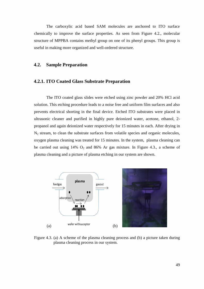
49
The carboxylic acid based SAM molecules are anchored to ITO surface
chemically to improve the surface properties. As seen from Figure 4.2., molecular
structure of MPPBA contains methyl group on one of its phenyl groups. This group is
useful in making more organized and well-ordered structure.
4.2. Sample Preparation
4.2.1. ITO Coated Glass Substrate Preparation
The ITO coated glass slides were etched using zinc powder and 20% HCl acid
solution. This etching procedure leads to a noise free and uniform film surfaces and also
prevents electrical shorting in the final device. Etched ITO substrates were placed in
ultrasonic cleaner and purified in highly pure deionized water, acetone, ethanol, 2-
propanol and again deionized water respectively for 15 minutes in each. After drying in
N2 stream, to clean the substrate surfaces from volatile species and organic molecules,
oxygen plasma cleaning was treated for 15 minutes. In the system, plasma cleaning can
be carried out using 14% O2 and 86% Ar gas mixture. In Figure 4.3., a scheme of
plasma cleaning and a picture of plasma etching in our system are shown.
(a) (b)
Figure 4.3. (a) A scheme of the plasma cleaning process and (b) a picture taken during
plasma cleaning process in our system.

50
4.2.2. SAM Formation
Cleaned ITO substrates were immediately dipped into 1mM ethanol solution of
MPPBA SAM molecule. Substrates were kept in this solution at room temperature for
48 hours. A chemical bounding was constituted on the hydroxyl-rich ITO surface from
the carboxylic acid head group of MPPBA molecules. The substrates were then rinsed
with ethanol to remove the residual MPPBA molecules from the ITO surface and finally
SAM modified ITO glass substrates were dried in a stream of N2 gas. The SAM
formation process is illustrated in Figure 4.4.
Figure 4.4. The self-assembly process
4.2.3. Deposition of Organic Layers
SAM modified ITO substrates were placed in organic evaporation system. TPD
or NPB organic HTL materials deposited under high vacuum (~ 10-6
Torr). Similarly, as
an ETL material Alq3 is deposited under high vacuum. Layers with 50 nm (for HTL)
and 40 nm (ETL) thickness were evaporated with low deposition rate (~ 0.5 Å/s).
Organic evaporation system used in the deposition of organic layers is shown in Figure
4.5.

51
Figure 4.5. Evaporation system for deposition of organic layers.
4.2.4. Deposition of Cathode Layer
High purity Al (99%) was thermally evaporated to form the top contact cathode
layer with a thickness of 120 nm at a pressure of 4×10⁻⁶
Torr and a deposition rate of 3
Å/s in evaporation system used during metal deposition. The photos taken from outside
and inside of the metal evaporation system are shown in Figure 4.6.
Figure 4.6. (a) Outside and (b) inside of metal evaporation system.
The mask used in Al evaporation and the top view of the final device is
illustrated in Figure 4.7.

52
Figure 4.7. (a) The mask used in Al cathode deposition and (b) top view of the final
device structure.
4.3. Characterization
4.3.1. Adsorption Kinetics of SAM Molecules
To indicate the adsorption kinetics of MPPBA molecules, delta frequency
change caused by the formation of SAM on ITO coated gold quartz crystal was
measured using Inficon Research Quartz Crystal Microbalance (RQCM). 5 MHz Ti/Au
polished quartz crystals were purchased from Inficon.
Two types of measurements were recorded; with static solutions and with fluidic
solutions. During the experiments prepared with static SAM solutions, 1 mM ethanolic
MPPBA solution with 0.3 ml volume dropped over the ITO coated QCM crystal with
the help of an injector and delta frequency change was recorded. To prevent any
environmental effect, top of the QCM cell closed. In the fluidic experiments, 1mM
MPPBA solution with the ratio of 0.2 μl/minute flowed through the silicon tubes with
the help of peristaltic pump and the frequency change was recorded. The used QCM and
peristaltic pump system is shown in Figure 4.8.

53
Figure 4.8. The Quartz Crystal Microbalance and peristaltic pump system.
4.3.2. AFM Surface Characterization (Topography and KPFM)
The surface morphology of the thin films was characterized by Solver Pro AFM
from NTMDT (Russia). The topography and the phase contrast images of the samples
were taken using NSG10 silicon tip with 30±5 μm cantilever width and typical 240 kHz
resonant frequency. KPFM mode of the AFM with TiN conducting cantilevers were
used to measure the change in the surface potential and work function before and after
modification of ITO surface. The AFM system was placed on a vibration-free table to
prevent environmental vibrations. Optic camera was used to project the image to the
computer screen and therefore the tip position was determined accurately on the sample.
AFM experimental setup is shown in Figure 4.9.
Figure 4.9. AFM and KPFM system.
54
To measure contact potential difference of the fabricated thin films, Solver P47H
atomic force microscope (NT-MTD) (Moscow, Russia) operating in semicontact mode
in air at room temperature was used. The tip side of the chip was Pt coated NSG01
silicon cantilevers (purchased from NT-MTD) with a 35nm nm tip curvature radius. The
resonance frequency of the tips was between 120 and 190 kHz. The scan rate was kept
constant at 1.01 Hertz during the operation. Two pass techniques were used in KPFM
experiments. In the first pass, topography image was obtained using standard
semicontact mode. And in the second pass, the probe was retracted from the surface in
the taken topography and the surface potential image of the substrate was obtained.
4.3.3. X-Ray Photoelectron Spectroscopy (XPS)
XPS is also known as Electron Spectroscopy Chemical Analysis (ESCA). It is a
very sensitive technique used for the chemical structure analysis of different surfaces.
As mentioned before XPS is based on photoelectric effect. When X-ray is sent to film
surface, the energy of core level electrons located at the orbitals rises up to the
ionization energy level. Electron that is reached to ionization energy is called as
photoelectron. With the calculation of the kinetic energy of photoelectrons that are
detected by photoelectron spectroscopy, binding energy of the removed electrons from
the surface can be obtained. Therefore, by using this technique elements found in a 1 to
10nm thick layer can be determined. For XPS technique Ultra high vacuum (< 10-9
Torr) system is needed.
For XPS analysis of MPPBA molecules, Microphysics Lab XPS system in
University of Illinois at Chicago (UIC) was used. The used XPS system is shown in
Figure 4.10.
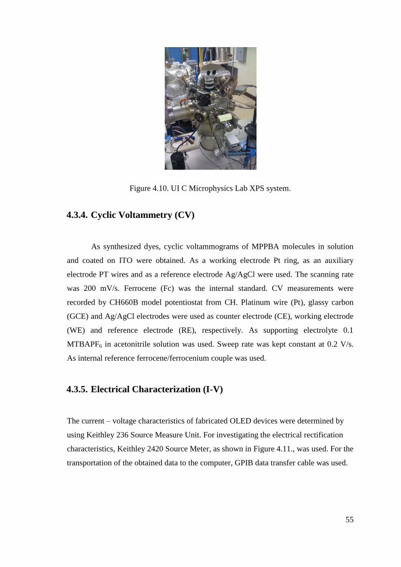
55
Figure 4.10. UI C Microphysics Lab XPS system.
4.3.4. Cyclic Voltammetry (CV)
As synthesized dyes, cyclic voltammograms of MPPBA molecules in solution
and coated on ITO were obtained. As a working electrode Pt ring, as an auxiliary
electrode PT wires and as a reference electrode Ag/AgCl were used. The scanning rate
was 200 mV/s. Ferrocene (Fc) was the internal standard. CV measurements were
recorded by CH660B model potentiostat from CH. Platinum wire (Pt), glassy carbon
(GCE) and Ag/AgCl electrodes were used as counter electrode (CE), working electrode
(WE) and reference electrode (RE), respectively. As supporting electrolyte 0.1
MTBAPF6 in acetonitrile solution was used. Sweep rate was kept constant at 0.2 V/s.
As internal reference ferrocene/ferrocenium couple was used.
4.3.5. Electrical Characterization (I-V)
The current – voltage characteristics of fabricated OLED devices were determined by
using Keithley 236 Source Measure Unit. For investigating the electrical rectification
characteristics, Keithley 2420 Source Meter, as shown in Figure 4.11., was used. For the
transportation of the obtained data to the computer, GPIB data transfer cable was used.

56
Figure 4.11. The Current-Voltage Measurement Setup.

57
CHAPTER 5
RESULTS AND DISCUSSION
5.1. Surface Characterization Results
5.1.1. Quartz Crystal Microbalance (QCM) Results
To investigate the SAM formation with quartz crystal microbalance (QCM)
technique, during our experiments, dynamic and static SAM solutions were used. From
the delta frequency change, the mass of the anchored MPPBA molecules are obtained.
Two different types of experiment setups were used to evaluate SAM formation. One of
them was carried on using MPPBA solution in flow and the other one was performed
with the stand by MPPBA solution.
In Figure 5.1., the delta frequency change obtained with the fluidic MPPBA
solution flow is shown. With MPPBA monolayer formation, significant negative
frequency change in the negative interval is obtained.
-500
-400
-300
-200
-100
0
100
0 10 20 30 40 50
MPPBA flowDelta F
requ
ency (
Hert
z)
Time (minutes)
Figure 5.1. Delta frequency vs. time plot of fluidic MPPBA solution.

58
From the Sauerbrey relation, delta frequency change was used to obtain total
mass change due to MPPBA monolayer. The calculated mass change versus time plot is
shown in Figure 5.2. The mass values of the formed monolayer molecules increases up
to 8 μgm/cm2 in 35 minutes and then get stable. These results enforce the SAM
formation on the ITO coated gold QCM crystal.
-2
0
2
4
6
8
10
0 10 20 30 40 50
MPPBA flow
Mass (
ugm
/cm
2)
Time (minutes)
Figure 5.2. Mass change vs. time plot with the formation of SAM monolayer.
In normal conditions, for the completion of SAM formation on ITO surfaces, 48
hour is the ideal waiting time. However, in QCM experiments, especially in stand by
solution experiments, after one hour later frequency signal breaks down because of the
leakage. Therefore, we carried out the experiments until the signal breaks down.
However, in the obtained delta frequency data, after the injection of the solution, no
significant frequency change is observed that represents the SAM formation.
In Figure 5.3., the delta frequency change that is obtained by the static MPPBA
SAM solution injection is shown. With the solution injection delta frequency decreases
up to -400 Hertz rapidly and then crystal temporizes the environment and gets stable at -
345 Hertz. The delta frequency stays constant for 40 minutes.

59
-500
-400
-300
-200
-100
0
100
0 10 20 30 40 50
stable MPPBA solution
De
lta F
req
ue
ncy (
He
rtz)
Time (minutes)
Figure 5.3. Delta frequency vs. time plot of static MPPBA solution.
The obtained mass change versus time graph is shown in Figure 5.4. The mass
change gets stable at 6μgm/cm2.
-2
0
2
4
6
8
0 5 10 15 20 25 30 35
stable MPPBA solution
Ma
ss (
ug
m/c
m2)
Time (minutes)
Figure 5.4. Mass change vs. time plot of stand by MPPBA SAM solution.

60
5.1.2. Atomic Force Microscopy (AFM) Results for Thin Films
For the surface investigation of surface morphology of the thin films, AFM
images were recorded. To distinguish the surface morphology differences caused by
SAM formation and HTL material deposition all AFM images for roughness analysis
were taken for 4x4 m2 and 2x2 m
2 scan areas.
Figure 5.5. shows the obtained surface topography and phase contrast images of
bare ITO surfaces. As seen from the topography image ITO has rough surface. The
measured surface roughness (rms) was found as 3.71 nm.
(a) (b)
(a) (b)
Figure 5.5. (a) Surface topography and (b) phase contrast image of bare ITO surface.
The surface topography and phase contrast images of MPPBA SAM modified
ITO surfaces are shown in Figure 5.6. Island like structures can be seen with the SAM

61
formation and surface properties of the ITO surface has changed. The average
roughness was measured as 3.41nm.
(a) (b)
(a) (b)
Figure 5.6. (a) Surface topography and (b) phase contrast image of MPPBA modified
ITO surface.
In Figure 5.7., the surface topography and phase contrast images of TPD coated
ITO surface are shown with 2 nm and 4 nm scan area. The ITO surface structure
changed with the TPD deposition. The surface roughness was measured as 1.282 nm.

62
(a) (b)
(a) (b)
Figure 5.7. (a) Surface topography and (b) phase contrast image of TPD coated ITO
surface.
Figure 5.8. represents the surface topography and phase contrast images of TPD
deposited on MPPBA modified ITO surface. The topography image looks like TPD
coated ITO surface but small molecule structures are clear. The roughness of the surface
is measured as 1.01 nm.

63
(a) (b)
(a) (b)
Figure 5.8. (a) Surface topography and (b) phase contrast image of MPPBA
modified/TPD coated ITO surface.
The surface topography and the phase contrast images of NPB coated ITO
surface are shown in Figure 5.9. The surface roughness is obtained as 2.22 nm.
Therefore, NPB coated films have more rough structure than TPD coated films.

64
(a) (b)
(a) (b)
Figure 5.9. (a) Surface topography and (b) phase contrast image of NPB coated ITO
surface.
Figure 5.10 shows the surface topography and phase contrast images of NPB
coated on MPPBA modified ITO surface. The roughness of the films was measured as
1.92 nm.

65
(a) (b)
(a) (b)
Figure 5.10. (a) Surface topography and (b) phase contrast image of MPPBA
modified/NPB coated ITO surface.
Table 5.1. summarizes the measured surface roughness values of the fabricated
thin films.
Table 5.1. Roughness values of fabricated thin films.
Thin Films Roughness (rms)
Bare ITO 3.71 nm
ITO/MPPBA 3.41 nm
ITO/TPD 1.28 nm
ITO/MPPBA/TPD 1.01 nm
ITO/NPB 2.22 nm
ITO/MPPBA/NPB 1.92 nm
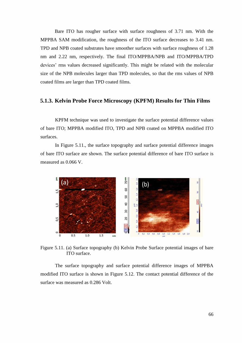
66
Bare ITO has rougher surface with surface roughness of 3.71 nm. With the
MPPBA SAM modification, the roughness of the ITO surface decreases to 3.41 nm.
TPD and NPB coated substrates have smoother surfaces with surface roughness of 1.28
nm and 2.22 nm, respectively. The final ITO/MPPBA/NPB and ITO/MPPBA/TPD
devices’ rms values decreased significantly. This might be related with the molecular
size of the NPB molecules larger than TPD molecules, so that the rms values of NPB
coated films are larger than TPD coated films.
5.1.3. Kelvin Probe Force Microscopy (KPFM) Results for Thin Films
KPFM technique was used to investigate the surface potential difference values
of bare ITO; MPPBA modified ITO, TPD and NPB coated on MPPBA modified ITO
surfaces.
In Figure 5.11., the surface topography and surface potential difference images
of bare ITO surface are shown. The surface potential difference of bare ITO surface is
measured as 0.066 V.
Figure 5.11. (a) Surface topography (b) Kelvin Probe Surface potential images of bare
ITO surface.
The surface topography and surface potential difference images of MPPBA
modified ITO surface is shown in Figure 5.12. The contact potential difference of the
surface was measured as 0.286 Volt.

67
Figure 5.12. (a) Surface topography (b) Kelvin Probe Surface potential images of
MPPBA modified ITO surface.
Figure 5.13. represents the surface topography and contact potential difference
images of TPD coated over MPPBA modified ITO surface. The contact surface
potential difference of the surface measured as 1.444 V.
Figure 5.13. (a) Surface topography and (b) Kelvin Probe Surface potential images of
MPPBA modified/TPD coated ITO surface.
Figure 5.14. shows the surface topography and contact potential difference
images of NPB coated over MPPBA modified ITO surface.

68
Figure 5.14. (a) Surface topography and (b) Kelvin Probe Surface potential images of
MPPBA modified/NPB coated ITO surface.
The Kelvin Probe Surface potential current versus Bias Voltage plots of bare
ITO and MPPBA modified ITO surfaces are shown in Figure 5.15. From the graph it is
clear that SAM modification increases the surface potential and therefore improves the
surface properties.
0
5
10
15
20
25
30
-0.5 0 0.5
ITO-MPPBA
Bare ITO
Ma
g(n
A)
Bias voltage(V)
Figure 5.15. Kelvin Probe Surface Potential Current-Voltage Plot.
Surface potential and measured rms values of fabricated thin films are
summarized in Table 5.2.

69
Table 5.2. Kelvin Probe Surface Potential values measured by KPFM Technique.
Surface Potential
(V)
Bare ITO 0.066
MPPBA modified ITO 0.286
MPPBA/TPD coated ITO 1.444
The results obtained by KPFM technique show the surface potential values are
changed from 0.066 V to 0.286 V after the modification of ITO surface with MPPBA
SAM molecules. These changes confirm the monolayer formation on ITO surface.
Additionally, an increase in the surface contact potential also indicates the increase in
the work function of the surface. Therefore, with the SAM modification, Fermi level of
the ITO surface approaches to the HOMO level of the organic layer and thus the carrier
injection improved with the decreasing threshold voltage.
5.1.4. X-ray Photoelectron Spectroscopy (XPS) Results
Investigation of the chemical structure of COOH-terminated MPPBA SAM
molecules on the ITO substrate was made using X-ray photoelectron spectroscopy
(XPS). Figure 5.16. shows an XPS survey spectrum of SAM-modified ITO surface after
the modification process. The peaks, In 3d5/2, Sn 3d5/2, O 1s, N 1s and C 1s are seen in
the spectra with binding energies 443.6, 485.6, 530.7, 398.4, and 284 eV, respectively.
Indium (In) and stannum (Sn) peaks confirm the existence of the MPPBA molecules.

70
Figure 5.16. XPS survey spectrum of MPPBA modified ITO surface.
High resolution spectra of C 1s peak is shown in Figure 5.17. The C peak was fit
with a background and mixed singlet peak. The peaks at positions 288.3, 285.6 and
284.6 eV are assigned to O–C=O, C−N or C−O and C−C, respectively. The peak at
288.3 eV indicates the covalent bonding of O–C=O. This bonding formed between
COOH-terminated MPPBA molecule and hydroxyl groups of the ITO surface.
Additionally, this peak is attributed to carbon of carboxyl group in the formulated
molecule. In order to explain the origin of the peaks in C 1s spectra, one should
consider the C 1s spectra in organic compounds. Similar chemical shifts can be found
for C 1s in a wide range of organic compound models (Clark, et al. 1976, Moussaif, et
al. 2000).
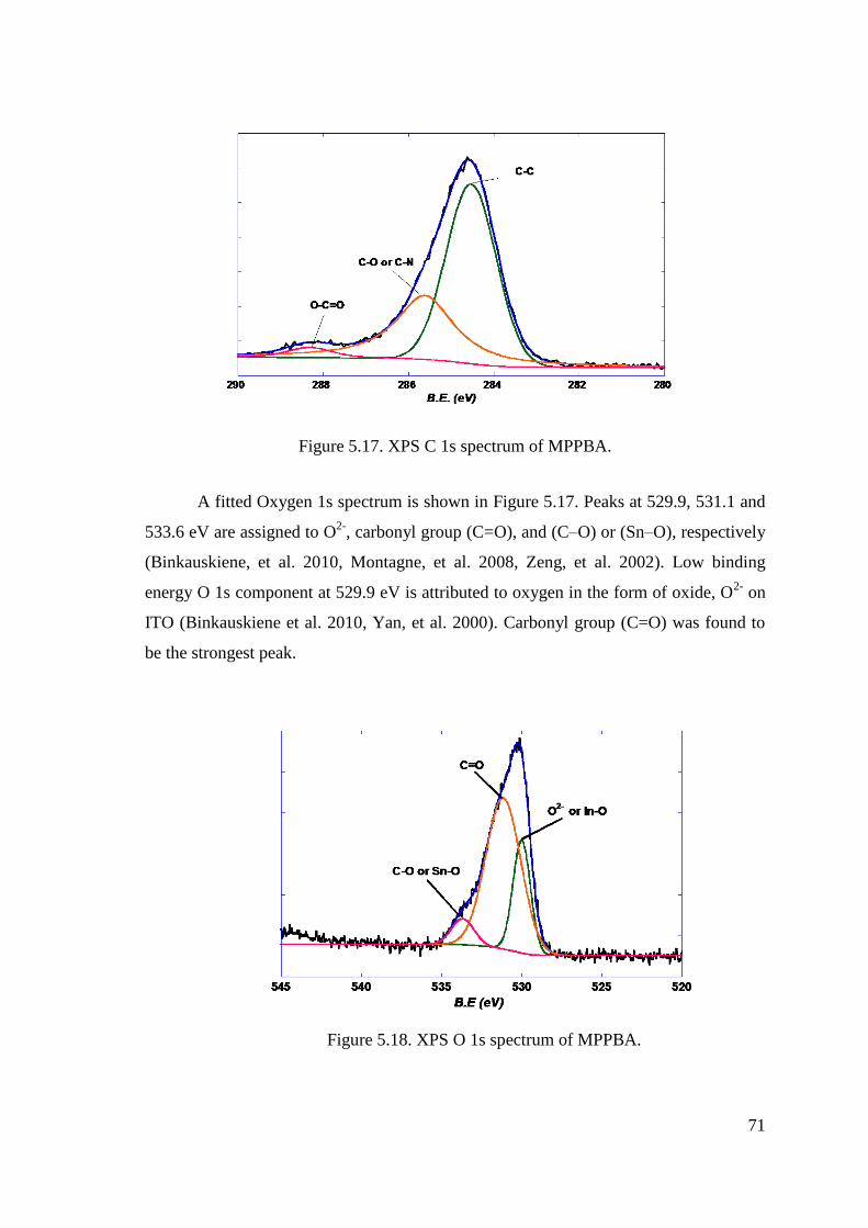
71
Figure 5.17. XPS C 1s spectrum of MPPBA.
A fitted Oxygen 1s spectrum is shown in Figure 5.17. Peaks at 529.9, 531.1 and
533.6 eV are assigned to O2-
, carbonyl group (C=O), and (C–O) or (Sn–O), respectively
(Binkauskiene, et al. 2010, Montagne, et al. 2008, Zeng, et al. 2002). Low binding
energy O 1s component at 529.9 eV is attributed to oxygen in the form of oxide, O2-
on
ITO (Binkauskiene et al. 2010, Yan, et al. 2000). Carbonyl group (C=O) was found to
be the strongest peak.
Figure 5.18. XPS O 1s spectrum of MPPBA.

72
5.1.5. Cyclic Voltammetry (CV) Results
Electrochemistry of MPPBA coated on ITO was studied by Cyclic Voltammetry
(CV). MPPBA molecules showed one reversible oxidation peak at 1.26 V in solution.
On the other hand, on ITO surface the oxidation peak was obtained at 1.15 V. This
slight shift toward more negative potential region can be attributed to the carbonyl
group that anchored to ITO surface. Electron affinity of carbonyl group decreases by
this binding and leads to decrease in oxidation potential compared to solution phase.
However, oxidation peak on ITO surface was observed to be quassi-reversible most
probably due to the formation unstable oxidized species of monolayer on ITO surface.
Figure 5.19. Cyclic voltammograms of the MPPBA (in solution) and MPPBA coated on
ITO surface.
It must be noticed that HOMO level of MPPBA was calculated from the onset
oxidation potential that is determined from the intersection of two tangents drawn from
rising oxidation current and background current in the cyclic voltammogram. The onset
of the oxidation was calculated to be 1.1 V in solution, while it was 0.99 V on ITO
surface. While HOMO level of MPPBA in solution was calculated as -5.51 eV, the
HOMO level of MPPBA on ITO surface was calculated as -5.4 eV. This situation may
be attributed to decrease in surface potential of ITO with the SAM formation.

73
5.1.6. Ultraviolet-Visible Spectroscopy (UV-Vis) Results
Analiytic Jena S 600 UV spectrophotometer was used to investigate the photo
physical and photochemical properties of synthesized MPPBA molecules. In Figure
5.20. the UV spectrum of MPPBA coated ITO surface is shown. Between 350-550 nm,
there is a distinct absorption peak that represents the chemical structure of the MPPBA
molecule.
Figure 5.20. UV spectrum of MPPBA coated ITO substrate.
5.2. Electrical Characterization Results of Organic Diodes
5.2.1. Electrical Rectification Characteristics
5.2.1.1. Schottky Thermal Injection Results
Schottky characteristics of the devices were investigated to calculate barrier
height after the surface modification with SAM molecules and HTL materials. As the
work function and barrier height values of the fabricated devices are close to each other,
plots are obtained symmetric at negative and positive applied voltage intervals.
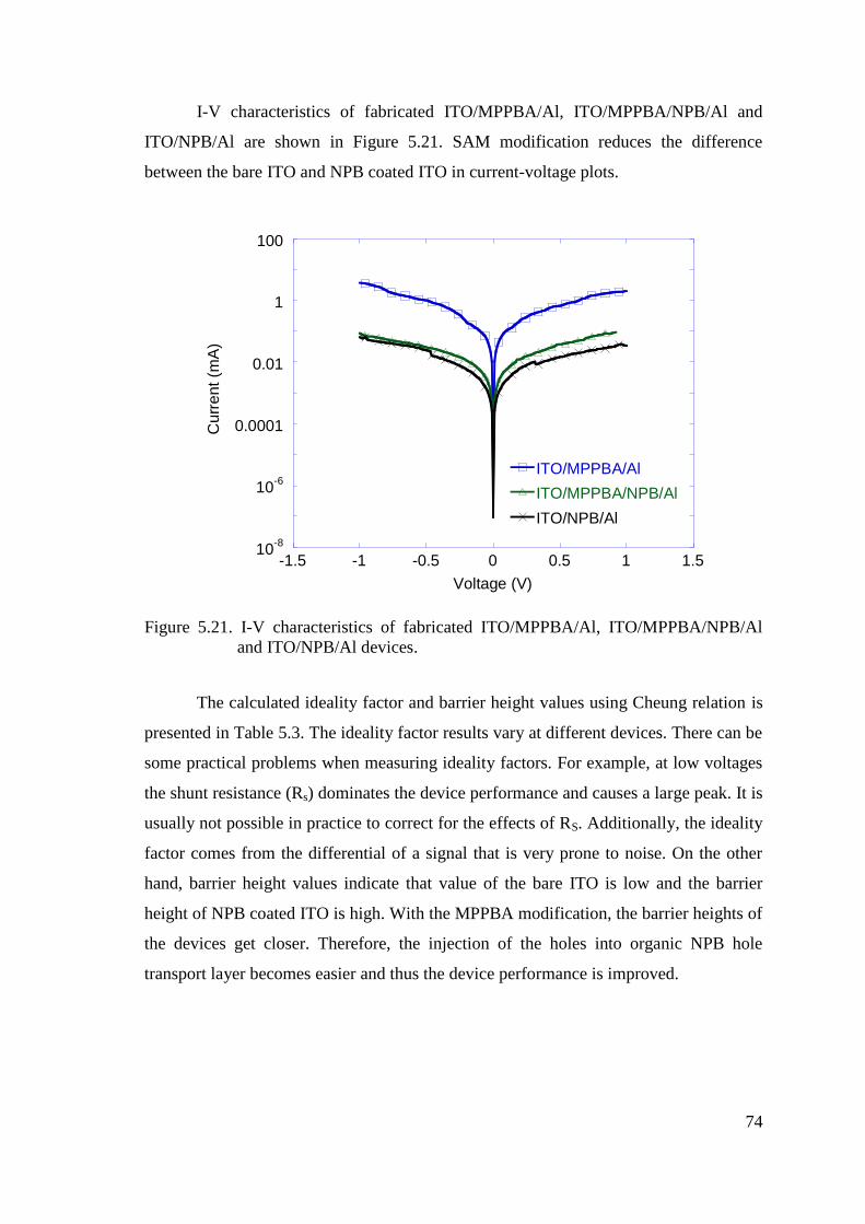
74
I-V characteristics of fabricated ITO/MPPBA/Al, ITO/MPPBA/NPB/Al and
ITO/NPB/Al are shown in Figure 5.21. SAM modification reduces the difference
between the bare ITO and NPB coated ITO in current-voltage plots.
10-8
10-6
0.0001
0.01
1
100
-1.5 -1 -0.5 0 0.5 1 1.5
ITO/MPPBA/Al
ITO/MPPBA/NPB/Al
ITO/NPB/Al
Cu
rre
nt
(mA
)
Voltage (V)
Figure 5.21. I-V characteristics of fabricated ITO/MPPBA/Al, ITO/MPPBA/NPB/Al
and ITO/NPB/Al devices.
The calculated ideality factor and barrier height values using Cheung relation is
presented in Table 5.3. The ideality factor results vary at different devices. There can be
some practical problems when measuring ideality factors. For example, at low voltages
the shunt resistance (Rs) dominates the device performance and causes a large peak. It is
usually not possible in practice to correct for the effects of RS. Additionally, the ideality
factor comes from the differential of a signal that is very prone to noise. On the other
hand, barrier height values indicate that value of the bare ITO is low and the barrier
height of NPB coated ITO is high. With the MPPBA modification, the barrier heights of
the devices get closer. Therefore, the injection of the holes into organic NPB hole
transport layer becomes easier and thus the device performance is improved.

75
Table 5.3. Calculated ideality factor and barrier height values of devices with NPB
organic layer.
ideality factor (n) barrier height (ΦB) (eV)
ITO/MPPBA/NPB/Al 2.28 0.503
ITO/NPB/Al 0.41 0.618
The Schottky characteristics of fabricated ITO/MPPBA/TPD/Al and
ITO/TPD/Al are shown in Figure 5.22. The surface modification made with MPPBA
SAM molecules reduces the conduction difference between ITO/AL and ITO/TPD/Al
devices.
10-7
10-6
10-5
0.0001
0.001
0.01
-1.5 -1 -0.5 0 0.5 1 1.5
ITO/MPPBA/Al
ITO/MPPBA/TPD/Al
ITO/TPD/Al
Cu
rre
nt
(mA
)
Voltage (V)
Figure 5.22. I-V characteristics of fabricated ITO/MPPBA/Al, ITO/MPPBA/TPD/Al
and ITO/TPD/Al devices.
The calculated ideality factor and barrier height values from I-V plot are shown
in Table 5.4. The barrier height between the ITO/Al and ITO/TPD/Al is minimized with
the MPPBA SAM modification. Like the devices prepared with SAM and NPB, the
transportation of the holes into organic TPD hole transport layer becomes easier and
thus the device efficiency increased.

76
Table 5.4. Calculated ideality factor and barrier height values of devices with TPD
organic layer.
ideality factor (n) barrier height (ΦB) (eV)
ITO/MPPBA/TPD/Al 4.64 0.508
ITO/TPD/Al 4.36 0.513
To investigate the variations caused by MPPBA molecules in different
structures, MPPBA modified n and p-type silicon substrates were used. In Figure 5.23.
the current-voltage relation of bare n-type silicon and MPPBA modified n-type silicon
is shown. In the reverse bias region, the conduction of the bare n-type silicon is better
than SAM modified one. On the other hand, under forward bias, the conduction in
MPPBA modified silicon is more efficient than the bare silicon. This observation
indicates that the use of SAM molecules can improve the surface properties of the
substrate. There is a little shift from the zero point of x-axis in bare n-type silicon. In
our experiments with silicon substrates we observed that the light in the environment of
the experiment setup affects the measurement results and thus this shifting can be
caused by the background light in the room.
0.0001
0.001
0.01
0.1
1
10
100
-6 -4 -2 0 2 4 6
n-type Si/Au
n-type Si/MPPBA/Au
Cu
rre
nt
(mA
)
Voltage (V)
Figure 5.23. Current-Voltage behavior of bare n-type silicon and MPPBA modified n-
type silicon.

77
The current-voltage behavior of bare p- and n-type silicon is shown in Figure
5.23. Again a shifting in x-axis caused by the light of environment is seen. MPPBA
modified p-type silicon device has better rectification behavior than bare p-type device
in the both reverse bias and forward bias region.
10-7
10-6
10-5
0.0001
0.001
0.01
0.1
1
10
-1.5 -1 -0.5 0 0.5 1 1.5
p-type Si/Au
p-type Si/MPPBA/Au
Cu
rre
nt
(mA
)
Voltage (V)
Figure 5.24. The Current-Voltage behavior of bare p-type silicon and MPPBA modified
p-type silicon devices.
The calculated ideality factor and barrier height values of untreated n- and p-
type devices and MPPBA modified n- and p-type devices are shown in Table 5.5. It is
obvious from the barrier height values, that SAM modification of the silicon substrates
alters the surface properties.
Table 5.5. The calculated ideality factor and barrier height values of bare and MPPBA
modified n-type and p-type silicon devices.
ideality factor (n) barrier height (ΦB) (eV)
Bare nSi/Au 1.00 0.670
nSi/MPPBA/Au 2.70 0.362
Bare pSi/Au 3.38 0.531
pSi/1 mM MPPBA/Au 2.48 0.594

78
5.2.1.2. Space Charge Limited Current Results
To evaluate the carrier mobility under steady state current in an organic
semiconductor, space-charge-limited current (SCLC) measurements were done up to 10
V.
In Figure 5.25., the current-voltage behavior of ITO/NPB/Al device is shown.
There is a significant increase in the forward bias region.
-0.01
0
0.01
0.02
0.03
0.04
0.05
0.06
0.07
-15 -10 -5 0 5 10 15
ITO/NPB/Al
Cu
rre
nt
(mA
)
Voltage (V)
Figure 5.25 . The Current-Voltage behavior ITO/NPB/Al between -10 and 10 V region.
The current-voltage characteristic of ITO/MPPBA/NPB/Al device is shown in
Figure 5.26. It has better rectification behavior than ITO/NPB/Al in forward bias region.
The current value reached to 110 mA at 10V.

79
-20
0
20
40
60
80
100
120
-15 -10 -5 0 5 10 15
ITO/MPPBA/NPB/Al
Curr
ent (m
A)
Voltage (V)
Figure 5.26. The Current-Voltage behavior ITO/MPPBA/NPB/Al between -10 and 10 V
region.
The comparison of the logarithmic graphs of J/E2 versus the square root of the
applied electric field for ITO/NPB/Al and ITO/MPPBA/NPB/Al devices are shown in
Figure 5.27. The effect of the SAM modification is noticeable.
-32
-30
-28
-26
-24
-22
1280 1300 1320 1340 1360 1380
ITO/MPPBA/NPB/Al
ITO/NPB/Al
ln(J
/E2)
(A/V
2)
[E(V/cm)]1/2
Figure 5.27. The logarithm of J/E2 versus the square root of the applied electric field for
ITO/NPB/Al and ITO/MPPBA/NPB/Al devices.
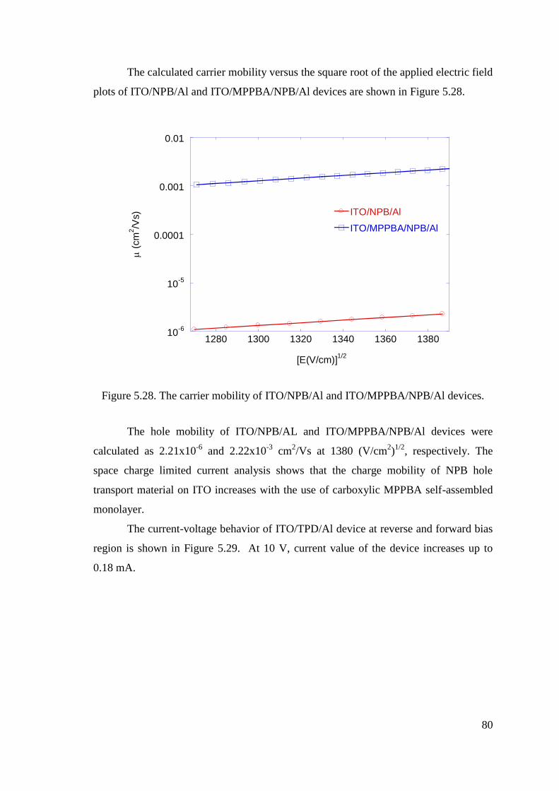
80
The calculated carrier mobility versus the square root of the applied electric field
plots of ITO/NPB/Al and ITO/MPPBA/NPB/Al devices are shown in Figure 5.28.
10-6
10-5
0.0001
0.001
0.01
1280 1300 1320 1340 1360 1380
ITO/NPB/Al
ITO/MPPBA/NPB/Al
(
cm
2/V
s)
[E(V/cm)]1/2
Figure 5.28. The carrier mobility of ITO/NPB/Al and ITO/MPPBA/NPB/Al devices.
The hole mobility of ITO/NPB/AL and ITO/MPPBA/NPB/Al devices were
calculated as 2.21x10⁻⁶
and 2.22x10⁻³
cm2/Vs at 1380 (V/cm
2)1/2
, respectively. The
space charge limited current analysis shows that the charge mobility of NPB hole
transport material on ITO increases with the use of carboxylic MPPBA self-assembled
monolayer.
The current-voltage behavior of ITO/TPD/Al device at reverse and forward bias
region is shown in Figure 5.29. At 10 V, current value of the device increases up to
0.18 mA.

81
-0.05
0
0.05
0.1
0.15
0.2
-10 -5 0 5 10 15
ITO/TPD/Al
Cu
rre
nt (m
A)
Voltage (V)
Figure 5.29. The Current-Voltage behavior ITO/TPD/Al between -10 and 10 V region.
In Figure 5.30. current-voltage characteristics of ITO/MPPBA/TPD/Al device is
shown. At the forward bias region, current value of the SAM modified device reaches at
0.4 mA.
-0.2
-0.1
0
0.1
0.2
0.3
0.4
0.5
-10 -5 0 5 10 15
ITO/MPPBA/TPD/Al
Cu
rre
nt
(mA
)
Voltage (V)
Figure 5.30. The Current-Voltage behavior ITO/MPPBA/TPD/Al between -10 and 10 V
region.

82
The comparison of the logarithmic graphs of J/E2 versus the square root of the
applied electric field for ITO/TPD/Al and ITO/MPPBA/TPD/Al devices are shown in
Figure 5.31. From the graph, it can be seen that MPPBA molecules modified the ITO
surface and changed the surface characteristics.
-29.5
-29
-28.5
-28
-27.5
1250 1300 1350 1400
ITO/TPD/Al
ITO/MPPBA/TPD/Al
ln(J
/E2)
(A/V
2)
[E(V/cm)]1/2
Figure 5.31. The logarithm of J/E2 versus the square root of the applied electric field for
ITO/TPD/Al and ITO/MPPBA/TPD/Al devices.
In Figure 5.32., the carrier mobility of ITO/TPD/Al and ITO/MPPBA/TPD/Al
devices versus the square root of applied electric field is shown. Again for the devices
made with TPD HTL material, SAM modification increases the hole mobility.

83
2 10-6
4 10-6
6 10-6
8 10-6
1 10-5
1.2 10-5
1.4 10-5
1250 1300 1350 1400
ITO/TPD/Al
ITO/MPPBA/TPD/Al
(
cm
2/V
s)
[E(V/cm)]1/2
Figure 5.32. The carrier mobility of ITO/TPD/Al and ITO/MPPBA/TPD/Al devices.
The carrier mobility of ITO/TPD/Al and ITO/MPPBA/TPD/Al devices at 1380
(V/cm) 1/2
applied electric field measured as 4.94x10⁻⁶
and 1.35x10⁻⁵
cm2/Vs, ı-V
respectively. Thus, the surface modification of ITO surface with carboxylic acid based
SAM increases the charge mobility.
5.2.2. Current-Voltage Characteristics of OLEDs with SAM Modified
ITO
The current-voltage characteristics of ITO/TPD (50nm)/Alq3 (60nm)/Al
(120nm) and ITO/MPPBA/TPD (50nm)/Alq3 (60nm)/Al (120nm) fabricated devices are
shown in Figure 5.33. The turn-on voltage of the ITO/TPD/Alq3/Al device was
measured as 5. 5 V while the turn on voltage of the ITO/MPPBA/TPD/Alq3/Al device
was measured as 4.5 V. Therefore, MPPBA modified device’s threshold voltage
improved about 1 V compared to the one made with bare ITO film. The increase in the
tunneling current density at the interface can be explained with inelastic tunneling
mechanism over extra energy levels between HOMO and LUMO of aromatic MPPBA
molecules with π-conjugated structure used as tunnel barrier at the interface.

84
-50
0
50
100
150
-5 0 5 10 15 20 25
ITO/TPD/Alq3/Al
ITO/MPPBA/TPD/Alq3/Al
Cu
rre
nt
De
nsity (
mA
/cm
2)
Voltage (V)
Figure 5.33. The Current density vs. voltage plot of devices fabricated with bare ITO
and MPPBA modified ITO substrates using TPD as HTL.
The electroluminescence intensity spectrums of the ITO/TPD/Alq3/Al and
ITO/MPPBA/TPD/Alq3/Al devices are shown in Figure 5.34. The maximum intensity
was observed around 525 nm due to the Alq3 emissive layer. Four times light intensity
enhancement was obtained as a result of modification of ITO surface using MPPBA
SAM molecule due to the increase in hole injection.
-1000
0
1000
2000
3000
4000
5000
0 200 400 600 800 1000 1200
ITO/TPD/Alq3/Al
ITO/MPPBA/TPD/Alq3/Al
Inte
nsity (
a.u
.)
Wavelength (nm)
Figure 5.34. The EL intensity spectrum of devices with bare ITO and MPPBA modified
ITO substrates using TPD as HTL.

85
The current-voltage behavior of ITO/NPB (50nm)/Alq3 (60nm)/Al (120nm) and
ITO/MPPBA/NPB (50nm)/Alq3 (60nm)/Al (120nm) fabricated devices are shown in
Figure 5.35. The turn-on voltage of the ITO/NPB/Alq3/Al device was measured as 9.3
V while the turn on voltage of the ITO/MPPBA/NPB/Alq3/Al device was measured as
7.3 V. Therefore, MPPBA modified device’s threshold voltage improved about 2 V
compared to the one made with bare ITO film.
-5
0
5
10
15
20
-5 0 5 10 15 20 25
ITO/NPB/Alq3/Al
ITO/MPPBA/NPB/Alq3/Al
Cu
rre
nt
De
nsity (
mA
/cm
2)
Voltage (V)
Figure 5.35. The Current density vs. voltage plot of devices fabricated with bare ITO
and MPPBA modified ITO substrates using NPB as HTL.
The electroluminescence intensity spectrums of the ITO/NPB/Alq3/Al and
ITO/MPPBA/NPB/Alq3/Al devices are shown in Figure 5.36. The maximum intensity is
observed around 530 nm again due to the Alq3 emissive layer. 2.5 times light intensity
enhancement was obtained as a result of modification of ITO surface using MPPBA
SAM molecule due to the increase in hole injection.

86
0
200
400
600
800
1000
1200
1400
1600
0 200 400 600 800 1000 1200
ITO/NPB/Alq3/Al
ITO/MPPBA/NPB/Alq3/Al
Inte
nsity (
a.u
)
Wavelenght (nm)
Figure 5.36. The EL intensity spectrum of devices with bare ITO and MPPBA
modified ITO substrates using NPB as HTL.

87
CHAPTER 6
CONCLUSION
This thesis has focused on the enhancement of efficiency and turn-on voltage of
OLEDs by modifying ITO surface with self-assembled monolayer molecules. In chapter
one, a brief overview about OLED technology was given and the research objectives of
the thesis have been discussed in details.
In chapter two, the advantages of OLEDs, history of the electroluminescence
and OLED technology have been discussed. The organic semiconductors, basic OLED
device structure, charge injection and recombination processes have been given in
details. In addition, OLED efficiency and light outcoupling have been explained.
In chapter three, SAM phenomenon has been discussed briefly. This chapter
consists of five subtitles; history of SAMs, types of SAMs, formation processes,
characterization and finally SAM applications were presented. In characterization part,
the basic operation theories of Quartz Crystal Microbalance (QCM), Atomic Force
Microscopy (AFM), Kelvin Probe Force Microscopy (KPFM), X-ray Photoelectron
Spectroscopy (XPS), Cyclic Voltammetry (CV) and Ultraviolet-visible Absorption
Spectroscopy (UV-Vis) techniques have been explained.
Chapter four is the part where experimental details have been presented. In
materials and chemical compounds part, the materials and the molecules that were used
in fabrication of OLED devices were introduced. In the sample preparation part,
substrate cleaning and preparation processes, SAM formation processes and deposition
of the organic and metal materials have been explained step by step. In characterization
part, technical properties of used systems and their apparatus have been given. The
SAM formation process, used mask shapes and used instruments were illustrated.
In chapter five, the experimental results were given with a detailed discussion
under two main subtitles with surface and electrical characterizations.
Surface characterization results obtained with QCM technique, the change in the
frequency due to the SAM formation presented. The total mass change during the
formation also calculated using Sauerbrey relation. In QCM experiments carried with

88
MPPBA solution in dynamic flow, the mass of the anchored SAM molecules on ITO
coated QCM crystal was measured as 8 μgm/cm2.
Topography and phase contrast images of fabricated thin films were performed
using AFM. The results show that bare ITO has rougher surface with surface roughness
of 3.71 nm. MPPBA molecules modify ITO surface leading to decrease up to 3.41 nm
in roughness values. As HTL materials (NPB and TPD) have smooth surface, the rms
value of the final thin films measured as 1.28 nm and 2.22 nm, respectively with the
SAM modification of ITO surface. As a result, the interface matching between the
anode and HTL has been provided.
Surface contact potential difference images of prepared thin films were obtained
using KPFM. The surface potential difference was changed from 0.066 V to 0.286 V
with MPPBA formation. Since contact surface potential proportional to the work
function of that surface, the work function of the ITO surface increased with MPPBA
modification, Fermi level of the ITO surface approaches to the HOMO level of the
organic layer and thus the carrier injection improved with the decreasing threshold
voltage.
The results obtained by X-ray photoelectron spectroscopy, Cyclic Voltammetry
and UV-Vis Absorption spectroscopy ensures the existence of MPPBA molecules on
the ITO surface after kept in SAM solution for 48 hours.
Electrical rectification characteristics of fabricated organic diodes were
investigated to determine the Schottky barrier characteristics, current-voltage behavior
of ITO/MPPBA/Al, ITO/TPD(NPB)/Al and ITO/MPPBA/TPD(NPB)/Al diodes
analyzing between -1 V and +1 V. In addition, comparison of bare and MPPBA
modified diodes prepared with n- and p-type silicon substrates and gold electrodes have
been presented. The ideality factor and barrier height results obtained from Schottky
characteristics indicate that barrier height difference between the anode and HTL was
reduced by MPPBA modification of anode substrate. Space-charge-limited current
(SCLC) analysis has been used to evaluate carrier mobility under steady state of current
in an organic layer. The I-V measurements were carried out between (-10) V and (+10)
V applied voltage. The hole mobility of ITO/NPB/AL and ITO/MPPBA/NPB/Al
devices were calculated as 2.21x10⁻⁶
and 2.22x10⁻³
cm2/Vs at 1380 (V/cm
2)1/2
,
respectively. The carrier mobility of ITO/TPD/Al and ITO/MPPBA/TPD/Al devices at
1380 (V/cm) 1/2
applied electric field measured as 4.94x10⁻⁶
and 1.35x10⁻⁵
cm2/Vs, I-V

89
respectively. Obtained carrier mobility values indicate that with the SAM modification,
charge injection from anode to the organic layer improved and thus device efficiency
increased.
OLED characteristics of fabricated ITO/TPD(NPB)/Alq3/Al and ITO/MPPBA/
TPD(NPB)/Alq3/Al organic light emitting diodes have been obtained. I-V results
indicate that, the threshold voltage of the diodes with TPD HTL material decreased
from 5.5 V to 4.5 V by modifying ITO surface with MPPBA molecules while the
threshold voltage of the diodes with NPB HTL material decreased from 9.3 V to 7.3 V.
Additionally, EL intensity results presented. SAM modified devices with TPD HTL
material have four times higher intensity than devices prepared with bare ITO anode
surface. In the devices with NPB HTL material 2.5 times light intensity enhancement
was obtained as a result of modification of ITO surface using MPPBA SAM molecule
due to the increase in hole injection.
To summarize, SAM was used to modify the ITO surface to match the work
functions of anode and the organic layers at the interface. Important improvements have
been achieved to increase the charge transport in OLED devices by using SAM
techniques. SAM forming molecules with π –conjugated structure can be used at the
interface to increase charge density due to extra energy levels between HOMO and
LUMO of aromatic molecules as a result of inelastic tunneling mechanism.

90
REFERENCES
Abkowitz, M., I. Chen, and J.H. Sharp. 1968. Electron Spin Resonance of the Organic
Semiconductor, Copper Phthalocyanine. The Journal of Chemical Physics.
48:4561.
Adachi, C., M.A. Baldo, M.E. Thompson, and S.R. Forrest. 2001. Nearly 100% internal
phosphorescence efficiency in an organic light-emitting device. Journal of
Applied Physics. 90:5048.
Agrawal, M., Y. Sun, S.R. Forrest, and P. Peumans. 2007. Enhanced outcoupling from
organic light-emitting diodes using aperiodic dielectric mirrors. Applied Physics
Letters. 90:241112.
Albrecht, T., and C. Quate. 1987. Atomic resolution imaging of a nonconductor by
atomic force microscopy. Journal of Applied Physics. 62:2599-2602.
Allara, D.L., and R.G. Nuzzo. 1985. Spontaneously organized molecular assemblies. 1.
Formation, dynamics, and physical properties of n-alkanoic acids adsorbed from
solution on an oxidized aluminum surface. Langmuir. 1:45-52.
Almeleh, N., and S. Harrison. 1966. Trapping effects in the organic semiconductor
triphenylene. Journal of Physics and Chemistry of Solids. 27:893-901.
An, Y., M. Chen, Q. Xue, and W. Liu. 2007. Preparation and self-assembly of
carboxylic acid-functionalized silica. Journal of colloid and interface science.
311:507-513.
Asemblon. 2005. (accessed: www.asemblon.com).
Aviram, A., and M.A. Ratner. 1974. Molecular rectifiers. Chemical physics letters.
29:277-283.
Aziz, H., Z. Popovic, C.P. Tripp, N.-X. Hu, A.-M. Hor, and G. Xu. 1998. Degradation
processes at the cathode/organic interface in organic light emitting devices with
Mg:Ag cathodes. Applied Physics Letters. 72:2642-2644.
Balasubramanian, N., and A. Subrahmanyam. 1989. Electrical and optical properties of
reactively evaporated indium tin oxide (ITO) films-dependence on substrate
temperature and tin concentration. Journal of Physics D: Applied Physics.
22:206.
Baldo, M., D. O'Brien, M. Thompson, and S. Forrest. 1999. Excitonic singlet-triplet
ratio in a semiconducting organic thin film. Physical Review B. 60:14422.
Baldo, M., D. O'brien, Y. You, A. Shoustikov, S. Sibley, M. Thompson, and S. Forrest.
1998. Highly efficient phosphorescent emission from organic electroluminescent
devices. Nature. 395:151-154.

91
Beebe, J.M., V.B. Engelkes, J. Liu, J.J. Gooding, P.K. Eggers, Y. Jun, X. Zhu, M.N.
Paddon-Row, and C.D. Frisbie. 2005. Length dependence of charge transport in
nanoscopic molecular junctions incorporating a series of rigid thiol-terminated
norbornylogs. The Journal of Physical Chemistry B. 109:5207-5215.
Beljonne, D., A. Ye, Z. Shuai, and J.L. Brédas. 2004. Chain Length Dependence of
Singlet and Triplet Exciton Formation Rates in Organic Light Emitting Diodes.
Advanced Functional Materials. 14:684-692.
Besbes, S., A. Ltaief, K. Reybier, L. Ponsonnet, N. Jaffrezic, J. Davenas, and H. Ben
Ouada. 2003. Injection modifications by ITO functionalization with a self-
assembled monolayer in OLEDs. Synthetic Metals. 138:197-200.
Bigelow, W., D. Pickett, and W. Zisman. 1946. Oleophobic monolayers* 1:: I. Films
adsorbed from solution in non-polar liquids. Journal of Colloid Science. 1:513-
538.
Binkauskiene, E., A. Lugauskas, M. Krunks, I.O. Acik, V. Jasulaitiene, and G. Saduikis.
2010. Interaction of Chrysosporium merdarium with titanium oxide surface.
Synthetic Metals. 160:906-910.
Binning, G., C. Quate, and C. Gerber. 1986. Atomic force microscopy. Phys. Rev. Lett.
56:930-933.
Bishop, A.R., and R.G. Nuzzo. 1996. Self-assembled monolayers: Recent developments
and applications. Current Opinion in Colloid & Interface Science. 1:127-136.
Blochwitz, J., T. Fritz, M. Pfeiffer, K. Leo, D. Alloway, P. Lee, and N. Armstrong.
2001. Interface electronic structure of organic semiconductors with controlled
doping levels. Organic Electronics. 2:97-104.
Blom, P.W.M., M.J.M. Jong, and C.T.H.F. Liedenbaum. 1998. Device physics of
polymer light-emitting diodes. Polymers for Advanced Technologies. 9:390-401.
Brandriss, S., and S. Margel. 1993. Synthesis and characterization of self-assembled
hydrophobic monolayer coatings on silica colloids. Langmuir. 9:1232-1240.
Brown, T.M., R.H. Friend, I.S. Millard, D.J. Lacey, J.H. Burroughes, and F. Cacialli.
2001. Efficient electron injection in blue-emitting polymer light-emitting diodes
with LiF/Ca/Al cathodes. Applied Physics Letters. 79:174-176.
Brown, T.M., J.S. Kim, R.H. Friend, F. Cacialli, R. Daik, and W.J. Feast. 1999. Built-in
field electroabsorption spectroscopy of polymer light-emitting diodes
incorporating a doped poly(3,4-ethylene dioxythiophene) hole injection layer.
Applied Physics Letters. 75:1679-1681.
Brütting, W., H. Riel, T. Beierlein, and W. Riess. 2001. Influence of trapped and
interfacial charges in organic multilayer light-emitting devices. Journal of
Applied Physics. 89:1704.

92
Burroughes, J., D. Bradley, A. Brown, R. Marks, K. Mackay, R. Friend, P. Burns, and
A. Holmes. 1990. Light-emitting diodes based on conjugated polymers. Nature.
347:539-541.
Burrows, P., G. Gu, S. Forrest, E. Vicenzi, and T. Zhou. 2000. Semitransparent
cathodes for organic light emitting devices. Journal of Applied Physics. 87:3080.
Carrard, M., S. Goncalves-Conto, L. Si-Ahmed, D. Ades, and A. Siove. 1999. Improved
stability of interfaces in organic light emitting diodes with high Tg materials and
self-assembled monolayers. Thin Solid Films. 352:189-194.
Carson, G., and S. Granick. 1989. Self assembly of octadecyltrichlorosilane films on
mica. Journal of Applied Polymer Science. 37:2767-2772.
Cavalleri, O., G. Gonella, S. Terreni, M. Vignolo, L. Floreano, A. Morgante, M.
Canepa, and R. Rolandi. 2004. High resolution X-ray photoelectron
spectroscopy of L-cysteine self-assembled films. Phys. Chem. Chem. Phys.
6:4042-4046.
Cerruti, M., C. Rhodes, M. Losego, A. Efremenko, J.P. Maria, D. Fischer, S. Franzen,
and J. Genzer. 2007. Influence of indium-tin oxide surface structure on the
ordering and coverage of carboxylic acid and thiol monolayers. Journal of
Physics D: Applied Physics. 40:4212.
Chen, S., L. Li, C.L. Boozer, and S. Jiang. 2001. Controlled chemical and structural
properties of mixed self-assembled monolayers by coadsorption of symmetric
and asymmetric disulfides on Au (111). The Journal of Physical Chemistry B.
105:2975-2980.
Cheung, S., and N. Cheung. 1986. Extraction of Schottky diode parameters from
forward current voltage characteristics. Applied Physics Letters. 49:85-87.
Chidsey, C.E.D., and D.N. Loiacono. 1990. Chemical functionality in self-assembled
monolayers: structural and electrochemical properties. Langmuir. 6:682-691.
Chkoda, L., C. Heske, M. Sokolowski, E. Umbach, F. Steuber, and J. Staudigel. 2000.
Work function of ITO substrates and band-offsets at the TPD/ITO interface
determined by photoelectron spectroscopy. Synthetic Metals. 111:315-319.
Clark, D., and H. Thomas. 1976. Applications of ESCA to polymer chemistry. X. Core
and valence energy levels of a series of polyacrylates. Journal of Polymer
Science: Polymer Chemistry Edition. 14:1671-1700.
Crispin, X., V. Geskin, A. Crispin, J. Cornil, R. Lazzaroni, W.R. Salaneck, and J.L.
Brédas. 2002. Characterization of the interface dipole at organic/metal
interfaces. Journal of the American Chemical Society. 124:8131-8141.
Cui, X., A. Primak, X. Zarate, J. Tomfohr, O. Sankey, A. Moore, T. Moore, D. Gust, L.
Nagahara, and S. Lindsay. 2002. Changes in the electronic properties of a

93
molecule when it is wired into a circuit. The Journal of Physical Chemistry B.
106:8609-8614.
Dobbertin, T., M. Kroeger, D. Heithecker, D. Schneider, D. Metzdorf, H. Neuner, E.
Becker, H.H. Johannes, and W. Kowalsky. 2003. Inverted top-emitting organic
light-emitting diodes using sputter-deposited anodes. Applied Physics Letters.
82:284.
Dubois, L.H., and R.G. Nuzzo. 1992. Synthesis, structure, and properties of model
organic surfaces. Annual Review of Physical Chemistry. 43:437-463.
Engelkes, V.B., J.M. Beebe, and C.D. Frisbie. 2004. Length-dependent transport in
molecular junctions based on SAMs of alkanethiols and alkanedithiols: Effect of
metal work function and applied bias on tunneling efficiency and contact
resistance. Journal of the American Chemical Society. 126:14287-14296.
Evans, S., S. Johnson, H. Ringsdorf, L. Williams, and H. Wolf. 1998. Photoswitching of
azobenzene derivatives formed on planar and colloidal gold surfaces. Langmuir.
14:6436-6440.
Fan, J.C.C., and J.B. Goodenough. 1977. X-ray photoemission spectroscopy studies of
Sn-doped indium-oxide films. Journal of Applied Physics. 48:3524-3531.
Feng, X. 2008. Development of 8-Hydroxyquinoline Metal Based Organic Light-
Emitting Diodes. In Department of Materials Science and Engineering. Vol.
Doctor of Philosophy. University of Toronto.
Finklea, H. 1996. Electroanalytical Chemistry. by AJ Bard and I. Rubinstein, Marcel
Dekker, New York. 19:109.
Finklea, H. 2000. In Encyclopedia of Analytical Chemistry: Applications, Theory and
Instrumentation. John Wiley & Sons, New York.
Finklea, H., L. Robinson, A. Blackburn, B. Richter, D. Allara, and T. Bright. 1986.
Formation of an organized monolayer by solution adsorption of
octadecyltrichlorosilane on gold: Electrochemical properties and structural
characterization. Langmuir. 2:239-244.
Ganzorig, C., K.J. Kwak, K. Yagi, and M. Fujihira. 2001. Fine tuning work function of
indium tin oxide by surface molecular design: Enhanced hole injection in
organic electroluminescent devices. Applied Physics Letters. 79:272.
Gelbart, W.M., and S.A. Rice. 1969. Some Formal Results in a Theory of Molecular
Rearrangements: Photoisomerism. The Journal of Chemical Physics. 50:4775-
4786.
Giebeler, C., H. Antoniadis, D.D.C. Bradley, and Y. Shirota. 1999. Influence of the hole
transport layer on the performance of organic light-emitting diodes. Journal of
Applied Physics. 85:608.

94
Goodman, F.O., and N. Garcia. 1991. Roles of the attractive and repulsive forces in
atomic-force microscopy. Physical Review B. 43:4728.
Griffiths, D.J. 2005. Introduction to quantum mechanics. Pearson Prentice Hall.
Gu, G., D. Garbuzov, P. Burrows, S. Venkatesh, S. Forrest, and M. Thompson. 1997.
High-external-quantum-efficiency organic light-emitting devices. Optics letters.
22:396-398.
Gun, J., R. Iscovici, and J. Sagiv. 1984. On the formation and structure of self-
assembling monolayers:: II. A comparative study of Langmuir--Blodgett and
adsorbed films using ellipsometry and IR reflection--absorption spectroscopy.
Journal of colloid and interface science. 101:201-213.
Gun, J., and J. Sagiv. 1986. On the formation and structure of self-assembling
monolayers:: III. Time of formation, solvent retention, and release. Journal of
colloid and interface science. 112:457-472.
Hacker, C.A., J.D. Batteas, J.C. Garno, M. Marquez, C.A. Richter, L.J. Richter, R.D.
van Zee, and C.D. Zangmeister. 2004. Structural and chemical characterization
of monofluoro-substituted oligo (phenylene-ethynylene) thiolate self-assembled
monolayers on gold. Langmuir. 20:6195-6205.
Haddock, N., B. Domercq, and B. Kippelen. 2005. High mobility C< sub> 60</sub>
organic field-effect transistors. Electronics Letters. 41:444-446.
Haitjema, H., and J. Elich. 1991. Physical properties of pyrolytically sprayed tin-doped
indium oxide coatings. Thin Solid Films. 205:93-100.
Haldi, A. 2008. Patternable electrophosphorescent organic light-emitting diodes with
solution-processed organic layers. Georgia Institute of Technology.
Hartmann, U. 1991. van der Waals interactions between sharp probes and flat sample
surfaces. Physical Review B. 43:2404.
Hatton, R.A., S.R. Day, M.A. Chesters, and M.R. Willis. 2001. Organic
electroluminescent devices: enhanced carrier injection using an organosilane self
assembled monolayer (SAM) derivatized ITO electrode. Thin Solid Films.
394:291-296.
He, G., M. Pfeiffer, K. Leo, M. Hofmann, J. Birnstock, R. Pudzich, and J. Salbeck.
2004. High-efficiency and low-voltage p i n electrophosphorescent organic
light-emitting diodes with double-emission layers. Applied Physics Letters.
85:3911.
He, P., S.D. Wang, W.K. Wong, C.S. Lee, and S.T. Lee. 2001. Vibrational and
photoemission study of the interface between phenyl diamine and indium tin
oxide. Applied Physics Letters. 79:1561-1563.

95
Higuch, M., S. Uekusa, R. Nakano, and K. Yokogawa. 1994. Postdeposition annealing
influence on sputtered indium tin oxide film characteristics. Jpn. J. Appi. Phys.
Vol. 33:302-306.
Ho, P.K.H., M. Granström, R.H. Friend, and N.C. Greenham. 1998. Ultrathin Self
Assembled Layers at the ITO Interface to Control Charge Injection and
Electroluminescence Efficiency in Polymer Light Emitting Diodes. Advanced
Materials. 10:769-774.
Hosokawa, C., H. Higashi, H. Nakamura, and T. Kusumoto. 1995. Highly efficient blue
electroluminescence from a distyrylarylene emitting layer with a new dopant.
Applied Physics Letters. 67:3853-3855.
Huang, Q., S. Reineke, K. Walzer, M. Pfeiffer, and K. Leo. 2006. Quantum efficiency
enhancement in top-emitting organic light-emitting diodes as a result of
enhanced intrinsic quantum yield. Applied Physics Letters. 89:263512.
Ishii, H., H. Oji, E. Ito, N. Hayashi, D. Yoshimura, and K. Seki. 2000. Energy level
alignment and band bending at model interfaces of organic electroluminescent
devices. Journal of Luminescence. 87-89:61-65.
Ishii, H., K. Sugiyama, E. Ito, and K. Seki. 1999. Energy level alignment and interfacial
electronic structures at organic/metal and organic/organic interfaces. Advanced
Materials. 11:605-625.
Jabbour, G., B. Kippelen, N. Armstrong, and N. Peyghambarian. 1998. Aluminum
based cathode structure for enhanced electron injection in electroluminescent
organic devices. Applied Physics Letters. 73:1185.
Kaifer, A.E., and M. Gómez-Kaifer. 1999. Supramolecular electrochemistry. Wiley
Online Library.
Kane, V., and P. Mulvaney. 1998. Double-layer interactions between self-assembled
monolayers of -mercaptoundecanoic acid on gold surfaces. Langmuir. 14:3303-
3311.
Kelley, T.W., P.F. Baude, C. Gerlach, D.E. Ender, D. Muyres, M.A. Haase, D.E. Vogel,
and S.D. Theiss. 2004. Recent progress in organic electronics: Materials,
devices, and processes. Chem. Mater. 16:4413-4422.
Kera, S., Y. Yabuuchi, H. Yamane, H. Setoyama, K. Okudaira, A. Kahn, and N. Ueno.
2004. Impact of an interface dipole layer on molecular level alignment at an
organic-conductor interface studied by ultraviolet photoemission spectroscopy.
Physical Review B. 70:085304.
Kim, J.S., P.K.H. Ho, N.C. Greenham, and R.H. Friend. 2000. Electroluminescence
emission pattern of organic light-emitting diodes: Implications for device
efficiency calculations. Journal of Applied Physics. 88:1073.

96
Krummacher, B., M. Mathai, V. Choong, S. Choulis, F. So, and A. Winnacker. 2006.
General method to evaluate substrate surface modification techniques for light
extraction enhancement of organic light emitting diodes. Journal of Applied
Physics. 100:054702.
Langevin, P. 1903. The ionisation of gases. Annales de Chimie et de Physique 28:289-
384.
Lee, J., B.J. Jung, J.I. Lee, H.Y. Chu, L.M. Do, and H.K. Shim. 2002. Modification of
an ITO anode with a hole-transporting SAM for improved OLED device
characteristics. Journal of Materials Chemistry. 12:3494-3498.
Li, D.Q., B.I. Swanson, J.M. Robinson, and M.A. Hoffbauer. 1993. Porphyrin based
self-assembled monolayer thin films: synthesis and characterization. Journal of
the American Chemical Society. 115:6975-6980.
Li, F., H. Tang, J. Anderegg, and J. Shinar. 1997a. Fabrication and electroluminescence
of double-layered organic light-emitting diodes with the AlO/Al cathode.
Applied Physics Letters. 70:1233.
Li, F., H. Tang, J. Shinar, O. Resto, and S.Z. Weisz. 1997b. Effects of aquaregia
treatment of indium--tin--oxide substrates on the behavior of double layered
organic light-emitting diodes. Applied Physics Letters. 70:2741-2743.
Madigan, C., M.H. Lu, and J. Sturm. 2000. Improvement of output coupling efficiency
of organic light-emitting diodes by backside substrate modification. Applied
Physics Letters. 76:1650-1652.
Mäkinen, A., I. Hill, R. Shashidhar, N. Nikolov, and Z. Kafafi. 2001. Hole injection
barriers at polymer anode/small molecule interfaces. Applied Physics Letters.
79:557.
Mark, F. 2001. Optical properties of solids. Oxford, Oxford University Press, New
York.
Marti, O., B. Drake, and P. Hansma. 1987. Atomic force microscopy of liquid covered
surfaces: Atomic resolution images. Applied Physics Letters. 51:484-486.
Mathauer, K., and C.W. Frank. 1993. Binary self-assembled monolayers as prepared by
successive adsorption of alkyltrichlorosilanes. Langmuir. 9:3446-3451.
McGinnes, J., P. Corry, and P. Proctor. 1974. Amorphous-semiconductor switching in
melanins. Science. 183:853-855.
Meulenkamp, E.A., R. van Aar, J.J.A.M. Bastiaansen, A. van den Biggelaar, H. Börner,
K. Brunner, M. BÜCHEL, A. van Dijken, N.M.M. Kiggen, and M. Kilitziraki.
2004. High efficiency polymer LEDs: triplets and novel devices. Society of
Photo-Optical Instrumentation Engineers. 90-103.

97
Meyer, G., and N.M. Amer. 1988. Novel optical approach to atomic force microscopy.
Applied Physics Letters. 53:1045-1047.
Milliron, D., I. Hill, C. Shen, A. Kahn, and J. Schwartz. 2000. Surface oxidation
activates indium tin oxide for hole injection. Journal of Applied Physics. 87:572.
Montagne, F., J. Polesel-Maris, R. Pugin, and H. Heinzelmann. 2008. Poly (N-
isopropylacrylamide) Thin Films Densely Grafted onto Gold Surface:
Preparation, Characterization, and Dynamic AFM Study of Temperature-
Induced Chain Conformational Changes. Langmuir. 25:983-991.
Mott, N.F., and R.W. Gurney. 1940. Electronic Processes in Ionic Crystal. Clarendon
PressOxford.
Moussaif, N., C. Pagnoulle, J. Riga, and R. Jérôme. 2000. XPS analysis of the
PC/PVDF interface modified by PMMA. Location of the PMMA at the
interface. Polymer. 41:3391-3394.
Mu, H. 2011. Carriers injection and transport in small molecule organic light emitting
diodes (OLED). Vol. Ph.D. University of Cincinnati, United States -- Ohio.
Nelson, S., Y.Y. Lin, D. Gundlach, and T. Jackson. 1998. Temperature-independent
transport in high-mobility pentacene transistors. Applied Physics Letters.
72:1854.
Nonnenmacher, M., M. Oboyle, and H. Wickramasinghe. 1991. Kelvin probe force
microscopy. Applied Physics Letters. 58:2921-2923.
Nüesch, F., E. Forsythe, Q. Le, Y. Gao, and L. Rothberg. 2000. Importance of indium
tin oxide surface acido basicity for charge injection into organic materials based
light emitting diodes. Journal of Applied Physics. 87:7973.
Ogawa, H., T. Chihara, and K. Taya. 1985. Selective monomethyl esterification of
dicarboxylic acids by use of monocarboxylate chemisorption on alumina.
Journal of the American Chemical Society. 107:1365-1369.
Osikowicz, W., X. Crispin, C. Tengstedt, L. Lindell, T. Kugler, and W.R. Salaneck.
2004. Transparent low-work-function indium tin oxide electrode obtained by
molecular scale interface engineering. Applied Physics Letters. 85:1616.
Oxtoby, D.W., W.A. Freeman, and T.F. Block. 2003. Chemistry: Science of Change.
Peisert, H., M. Knupfer, F. Zhang, A. Petr, L. Dunsch, and J. Fink. 2004. The interface
between phthalocyanines and PEDOT: PSS: evidence for charge transfer and
doping. Surface science. 566:554-559.
Piromreun, P., H. Oh, Y. Shen, G.G. Malliaras, J.C. Scott, and P.J. Brock. 2000. Role of
CsF on electron injection into a conjugated polymer. Applied Physics Letters.
77:2403-2405.

98
Pope, M., H.P. Kallmann, and P. Magnante. 1963. Electroluminescence in Organic
Crystals. Journal of Chemical Physics. 38:2042-2043.
Pope, M., and C.E. Swenberg. 1999. Electronic processes in organic crystals and
polymers. Oxford University Press Oxford.
Rhoderick, E.H., and R. Williams. 1988. Metal-semiconductor contacts. Clarendon
Press Oxford.
Riel, H., S. Karg, T. Beierlein, B. Ruhstaller, and W. Rieß. 2003. Phosphorescent top-
emitting organic light-emitting devices with improved light outcoupling. Applied
Physics Letters. 82:466.
Sabatani, E., I. Rubinstein, R. Maoz, and J. Sagiv. 1987. Organized self-assembling
monolayers on electrodes. I: Octadecyl derivatives on gold. Journal of
electroanalytical chemistry and interfacial electrochemistry. 219:365-371.
Sagiv, J. 1980. Organized monolayers by adsorption. 1. Formation and structure of
oleophobic mixed monolayers on solid surfaces. Journal of the American
Chemical Society. 102:92-98.
Salaneck, W.R., and J.L. Brédas. 1996. The metal on polymer interface in polymer light
emitting diodes. Advanced Materials. 8:48-52.
Sauerbrey, G. 1959. Use of quartz vibrator for weighing thin films on a microbalance.
Z. Phys. 155:206-210.
Schlotter, N., M.D. Porter, T. Bright, and D.L. Allara. 1986. Formation and structure of
a spontaneously adsorbed monolayer of arachidic on silver. Chemical physics
letters. 132:93-98.
Schwartz, D., S. Steinberg, J. Israelachvili, and J. Zasadzinski. 1992. Growth of a self-
assembled monolayer by fractal aggregation. Physical review letters. 69:3354-
3357.
Scott, J.C. 2003. Metal-organic interface and charge injection in organic electronic
devices. Journal of Vacuum Science & Technology A: Vacuum, Surfaces, and
Films. 21:521.
Scott, J.C., P.J. Brock, J.R. Salem, S. Ramos, G.G. Malliaras, S.A. Carter, and L.
Bozano. 2000. Charge transport processes in organic light-emitting devices.
Synthetic Metals. 111:289-293.
Shinar, J. 2004. Organic light-emitting devices: a survey. Springer Verlag.
Shipway, A., M. Lahav, and I. Willner. 2000. Nanostructured gold colloid electrodes.
Advanced Materials. 12:993-998.
Shirakawa, H., E.J. Louis, A.G. MacDiarmid, C.K. Chiang, and A.J. Heeger. 1977.
Synthesis of electrically conducting organic polymers: halogen derivatives of
99
polyacetylene,(CH) x. Journal of the Chemical Society, Chemical
Communications. 1977:578-580.
Singh, A. 2009. Electrical and Optical properties of electroluminescent materials used
for Organic Light Emitting Device. In Materials Science and Engineering. Vol.
Master of Technology. School of Physics and Material Science Thapar
University, India.
Smith, L., J. Wasey, and W.L. Barnes. 2004. Light outcoupling efficiency of top-
emitting organic light-emitting diodes. Applied Physics Letters. 84:2986-2988.
Snook, G.A. 2000. Investigation of Solid-State Reactions by Electrochemical and
Quartz Crystal
Microbalance Measurements. In Department of Chemistry. Vol. B.Sc. Monash
University, Melbourne.
Sreenivas, K., T.S. Rao, A. Mansingh, and S. Chandra. 1985. Preparation and
characterization of rf sputtered indium tin oxide films. Journal of Applied
Physics. 57:384-392.
Subramanian, V., E. Wolf, and P.V. Kamat. 2001. Semiconductor-metal composite
nanostructures. To what extent do metal nanoparticles improve the
photocatalytic activity of TiO2 films? The Journal of Physical Chemistry B.
105:11439-11446.
Sugiyama, K., H. Ishii, Y. Ouchi, and K. Seki. 2000. Dependence of indium-tin-oxide
work function on surface cleaning method as studied by ultraviolet and x-ray
photoemission spectroscopies. Journal of Applied Physics. 87:295.
Sun, X., L. Cheng, M. Liu, L. Liao, N. Wong, C. Lee, and S. Lee. 2003. Photoelectron
spectroscopic study of iodine-and bromine-treated indium tin oxides and their
interfaces with organic films. Chemical physics letters. 370:425-430.
Suzuki, H. 1996. Fabrication of electron injecting Mg:Ag alloy electrodes for organic
light-emitting diodes with radio frequency magnetron sputter deposition.
Applied Physics Letters. 69:1611-1613.
Swenberg, C., and M. Pope. 1999. Electronic Processes of Organic Crystals and
Polymers. Oxford University Press, Oxford.
Szczyrbowski, J., A. Dietrich, and H. Hoffmann. 1983. Optical and electrical properties
of RF sputtered indium-tin oxide films. physica status solidi (a). 78:243-252.
Sze, S. 1981. Physics of semiconductor devices. 1981. Wiley, New York.
Tang, C.W., and S.A.V. Slyke. 1987. Organic electroluminescent diodes. Applied
Physics Letters. 51:913.

100
Thiruvengadam, S. 2002. Characterization and Analysis of Hybrid Electronic Materials
For Molecular Based Devices In The Department of Electrical and Computer
Engineering. Louisiana State University, India.
Tillman, N., A. Ulman, J.S. Schildkraut, and T.L. Penner. 1988. Incorporation of
phenoxy groups in self-assembled monolayers of trichlorosilane derivatives.
Effects on film thickness, wettability, and molecular orientation. Journal of the
American Chemical Society. 110:6136-6144.
Tlili, A., A. Abdelghani, S. Hleli, and M.A. Maaref. 2004. Electrical characterization of
a thiol SAM on gold as a first step for the fabrication of an immunosensors
based on a quartz crystal microbalance. Sensors. 4:105-114.
Tsutsui, T., M. Yahiro, H. Yokogawa, K. Kawano, and M. Yokoyama. 2001. Doubling
Coupling Out Efficiency in Organic Light Emitting Devices Using a Thin Silica
Aerogel Layer. Advanced Materials. 13:1149-1152.
Turak, A., D. Grozea, X.D. Feng, Z.H. Lu, H. Aziz, and A.M. Hor. 2002.
Metal/AlQ[sub 3] interface structures. Applied Physics Letters. 81:766-768.
Ulman, A. 1996. Formation and structure of self-assembled monolayers. Chemical
reviews. 96:1533-1554.
Ulman, A., S.D. Evans, Y. Shnidman, R. Sharma, J.E. Eilers, and J.C. Chang. 1991.
Concentration-driven surface transition in the wetting of mixed alkanethiol
monolayers on gold. Journal of the American Chemical Society. 113:1499-1506.
Vincett, P., W. Barlow, R. Hann, and G. Roberts. 1982. Electrical conduction and low
voltage blue electroluminescence in vacuum-deposited organic films. Thin Solid
Films. 94:171-183.
Wang, P.W., Y.J. Liu, C. Devadoss, P. Bharathi, and J.S. Moore. 1996.
Electroluminescent diodes from a single component emitting layer of dendritic
macromolecules. Advanced Materials. 8:237-241.
Wasserman, S.R., Y.T. Tao, and G.M. Whitesides. 1989. Structure and reactivity of
alkylsiloxane monolayers formed by reaction of alkyltrichlorosilanes on silicon
substrates. Langmuir. 5:1074-1087.
Weisenhorn, A.L., M. Egger, F. Ohnesorge, S. Gould, S. Heyn, H. Hansma, R.
Sinsheimer, H. Gaub, and P. Hansma. 1991. Molecular-resolution images of
Langmuir-Blodgett films and DNA by atomic force microscopy. Langmuir. 7:8-
12.
White, H.S., J.D. Peterson, Q. Cui, and K.J. Stevenson. 1998. Voltammetric
measurement of interfacial acid/base reactions. The Journal of Physical
Chemistry B. 102:2930-2934.

101
Wold, D.J., and C.D. Frisbie. 2001. Fabrication and characterization of metal-molecule-
metal junctions by conducting probe atomic force microscopy. Journal of the
American Chemical Society. 123:5549-5556.
Wu, C., C. Wu, J. Sturm, and A. Kahn. 1997. Surface modification of indium tin oxide
by plasma treatment: An effective method to improve the efficiency, brightness,
and reliability of organic light emitting devices. Applied Physics Letters.
70:1348.
Yan, C., M. Zharnikov, A. Gölzhäuser, and M. Grunze. 2000. Preparation and
characterization of self-assembled monolayers on indium tin oxide. Langmuir.
16:6208-6215.
Zeng, D., K. Yung, and C. Xie. 2002. XPS investigation of the chemical characteristics
of Kapton films ablated by a pulsed TEA CO2 laser. Surface and Coatings
Technology. 153:210-216.
Zou, L., V. Savvate'ev, J. Booher, C.H. Kim, and J. Shinar. 2001. Combinatorial
fabrication and studies of intense efficient ultraviolet--violet organic light-
emitting device arrays. Applied Physics Letters. 79:2282-2284.