Embed Size (px)
Citation preview

Characterization of Nanomaterials
Dr. Naveen Kumar Navani Assistant Professor, Department of Biotechnology Indian Institute of Technology Roorkee, Roorkee – 247 667
The future of nanotechnology rests upon approaches to making new, useful nanomaterials and testing them in complex systems. However, precise and trusting nanoparticle formation can only be promised after their thorough characterization. Here some of the basic physical and biophysical techniques are briefed which will be central to nanoparticles research.
1. X-ray Diffraction
The genesis of XRD can be traced to the suggestion of Max von Laue in 1912 that a crystal can be considered as a three-dimensional diffraction grating. It is generally used for qualitative analysis.X-ray diffraction (XRD) method is the most basic method for characterizing the crystal structures. X-rays corresponds to electromagnetic radiation in the wavelength range of 1 Å. The wavelength range is below that of ultraviolet light and above that of gamma rays.
X-rays are generally produced when electrons of several thousands of electron volts are decelerated or stopped by metals. This will produce a white radiation up to a threshold frequency corresponding to the kinetic energy of the particle. This threshold corresponds to a wavelength (in angstroms)
= 12399/V
Where,V-accelerating voltage of the electrons.
When electrons fall on matter with high energy, electrons can be ejected from various energy levels. Electron ejection from the core orbital is also accompanied by the emission of characteristic X-rays. (Fig.1)

XRD metelectrons crystal, wpeaks can
main com
are conn
The X-rayreflected r
In the Deevery pos
In the mointensity intensity aand comp
The partic
Where t
thod is basedbelonging to
where the atomn be uniquely
mponent of ma
nected with ea
y diffraction radiation. In e
bye-Scherrer sible set of la
odern diffractas a functionat this point a
pared with stan
cle size is obt
-thickness of
Figure 1- El
d on the measo the atoms ims are periodassigned to t
aterials. The
ach other by t
experiment each of these
method of dattice planes e
tion method n of diffractiare the two facndards in the
ained as broa
the crystallite
ectron beam
surements of n the materiadically arrangthe material. T
diffraction an
the Bragg’s la
n
requires the cases, there c
diffraction, weexposed to the
called diffracon angle is mctors used in literature.
adening of the
t = 0
e in (angstrom
m induced pro
X-ray intensial. Since the ged, the patteTherefore, XR
ngle 2, the i
aw
n=2dsin
following: a can be several
e use a monoe radiation.
ctometry, a cmeasured. Ththe determina
e diffracted lin
.9 / (Bcos)
ms)
ocesses in the
ities scatteredmost stable
ern of the poRD measurem
interplanar di
radiation, a l variations.
ochromatic X
convergent behe position oation. Both th
nes and is giv
)
e sample
d by the statistructure of
ositions and iment is impor
istance d and
sample and
X-ray and a po
eam strikes thof the diffrachese can be m
ven by the Sch
istically distria pure mater
intensities of rtant to identi
X-ray wavel
a detector fo
owder sample
he sample anction peak an
measured accu
herrer formul
ibuted rial is XRD fy the
length
or the
e with
nd the nd the urately
la,

-
B
The width
Thus, info
2. Micros
2.1 E
Transmis
The propegrain boucharacterian equipm(80–3,000
-Bragg’s angl
B –peak broad
h of the diffra
ormation obta
scopy
ELECTRON
ssion electron
erties of polyundaries andization of graiment to let th0 kV) which
le.
ening; full wi
action curve (B
Figure 2-
ained from XR
MICROSCO
n microscopy
crystalline md their non-pin boundaries
he incident elresults in gen
idth at intensi
B) (Fig.2) inc
Effect of par
RD can be us
OPY-
y
material are difperiodic arras and assists tectron beam nerating sign
ity half maxim
creases as the
rticle size on
ed to determi
fferent from tangements othe developmto transmit a
nals caused by
ma
e thickness of
diffraction c
ine the crystal
that of singlef atoms TEent of new po
a thin specimy the interact
f the crystal de
curves
l structure of
e crystalline mEM plays imolycrystalline
men at high-action between
ecreases.
the sample.
material, due mportant rolee materials. TEcceleration vo the specime
to the es for EM is oltage
en and

incident ethese sign
Uwin
Ethdisuanspinin
Insp
Figure 3-
electrons. Strunals. In genera
Unscattered elwithout any inversely prop
Elastically scahe specimen iffraction lawurface. All elengle. These “pots; each spnformation abnterest.
nelastically scpecimen with
a. The inThese extract
b. AnothKikuchthe ato
- Interaction
uctures, compal, there are th
lectrons- are interaction ocortional to the
ttered electrowithout losin
w. All incidenectrons that a“the same anpot corresponbout the orie
cattered electh losing their enelastic loss energies are t both compoer one is thehi bands. The
omic spacing
between inci
positions and hree types of
caused by inccurring insie specimen th
ons- are causeng energy. T
nt electrons haare scattered bngle” scatterending to a sentation, atom
trons- are cauenergy. Theseof energy byunique to eacsitional and c
e formation oese bands are in the specim
ident electro
chemical bontransmitted e
ncident electride the specihickness
ed by the inciThese elasticaave the same by the same aed electrons aspecific atommic arrangem
used by the ine provide twoy the incidench bonding stchemical bondof bands with
also formed men
on beam and
nds of the speelectrons obse
rons transmitimen. Amou
ident electronally scatteredenergy and e
atomic spacinare gathered
mic spacing. ments and ph
ncident electro types of infont electrons, tate of each eding informath alternating by inelastic s
specimen in
ecimen can berved by TEM
tted through unt of unscat
ns that are scad electrons foenter the specng will be sca
by lens and This diffrac
hases present
rons that inteormation. characteristic
element and ttion of the spelight and darscattering inte
case of TEM
be determinedM (Fig.3)-
the thin specttered electro
attered by atofollow the Brcimen normalattered by the
form a pattected pattern yt in the regi
eract with ato
c of the elemthus can be usecimen. rk lines, knoweractions rela
M
d from
cimen ons is
oms in ragg’s l to its same ern of yields on of
oms in
ments. sed to
wn as ated to

Tbe recombcontrast imbeams. ThThis imagremove althe particadvantagetechnique
2.2 Scann
Scanning of signalinteractioncompositiapplicatioimage is performinqualitativeanalysis).
The intera
There are two bined at the image of the ohis is achievege is called thll diffracted ecular diffractee of the darke is usually us
ning electron
electron micrls at the sns reveal infion, and crysons, data are
generated thng analyses oely or semi
actions exploi
main mechanimage plane, object. An amed by placinghe bright fieldelectron beamed beam of k-field imagied for observ
a) B
Figure
n microscopy
roscope (SEMsurface of sformation abostalline struccollected ove
hat displays of selected pi-quantitative
ited for SEM
nisms of contrthus preservi
mplitude contg suitable aped image. The
ms caused by tinterest. The
ing method iving grain size
Bright field
e 4- Different
-
M) uses a focsolid specimout the sampcture and orier a selected spatial variat
point locationly determini
analysis inclu
rast in an imaing their amptrast image caertures belowsize of the o
the specimen e image usingis its high-die distributions
b
t modes of im
cused beam ofmens. The s
ple includingientation of marea of the s
tions in thesns on the saming chemica
ude-
age. The transplitudes and pan be obtaine
w the back foobjective aperOne can alsog this is califfraction cons and dislocat
b) Dark field
maging in TE
f high-energysignals that g external mmaterials masurface of the properties. mple; this apal compositio
smitted and scphases. This red by eliminacal plane of rture should bo exclude all olled the darkntrast. The dtions (Fig.4)
d
EM
y electrons toderive from
morphology (aking up thehe sample, an The SEM i
pproach is esons (using E
cattered beamresults in the ating the diffrthe objective
be small enouother beams e
k field imagedark-field im
o generate a vm electron-sa(texture), chee sample. In nd a 2-dimensis also capabspecially useEnergy Dispe
ms can phase
fracted e lens. ugh to except e. The
maging
variety ample emical
most sional ble of ful in ersive
St
B D
mSEM analnot lead to
Essential
E E S D D In
Secondary eletopography onBackscatteredDiffracted baminerals lysis is consio volume loss
components o
Electron SourcElectron Lense
ample Stage Detectors for aDisplay / Data nfrastructure R
o Poo Vao Co
ectrons (that n samples d electrons - ilckscattered e
dered to be "s of the sampl
Fig
of all SEMs in
ce ("Gun") es
all signals of ioutput devic
Requirementsower Supply acuum Systemooling system
produce SEM
llustrating conelectrons- are
"non-destructile, so it is pos
5- Schematic
nclude the fo
interest es s:
m m
M images)- m
ntrasts in comused to dete
ive"; that is, ssible to analy
c representat
llowing (Fig.
most valuable
mposition in mermine crysta
x-rays generayze the same
tion of SEM
5)-
e for showing
multiphase saal structures a
ated by electrmaterials rep
g morpholog
amples and orientatio
ron interactiopeatedly.
gy and
ons of
ons do
Sample pinsulatingsome otheacquired fmost effec
SEM find
1. R2. T3. T4. Pr
acSEM high v
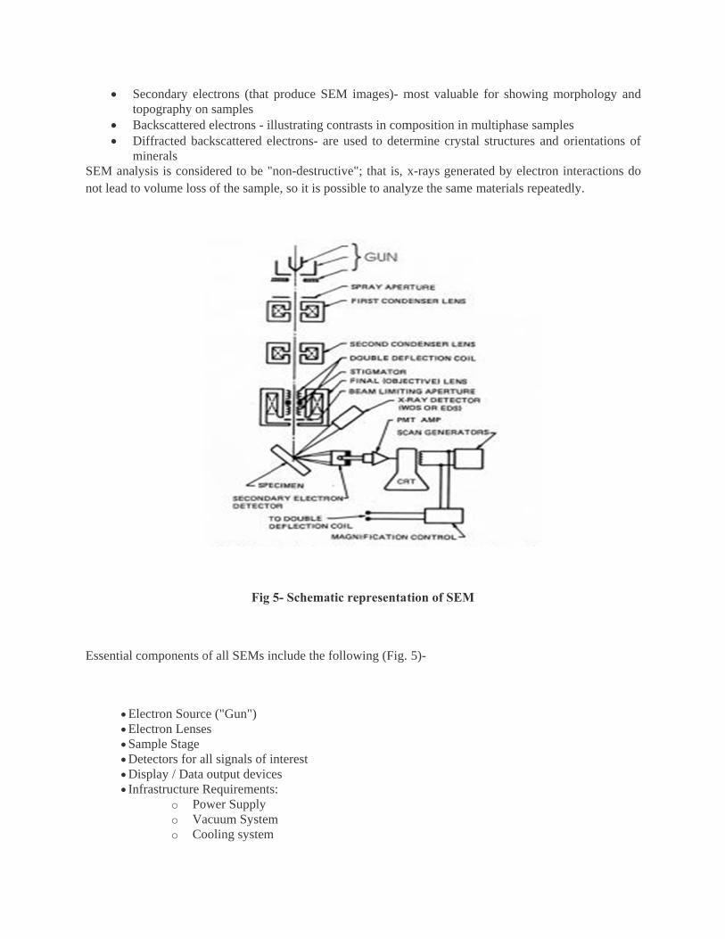
2.3Atomi
AFM pro(<10 nm)supportedbetween t
o Vio Ro
reparation fog samples areer metal or alfor eg.-carbonctive for high
ds use for vari
Routinely usedTo show spatiaTo identify pha
recise measuccomplished uoffers advant
vacuum requi
ic force micr
vides a 3D p) and surfaced on a flexiblethe probe and
ibration-free foom free of am
r SEM is a ce coated withlloy. The chon is most des
h resolution el
ied application
d to generate hal variations iases based onurement of vusing the SEMtage of wide irement of the
oscopy-
profile of the e at very she cantilever. the surface.
floor mbient magn
crucial task ina thin layer
oice of materisirable if elemlectron imagin
ns some of th
high-resolutioin chemical con qualitative cvery small fM. applicability
e order 10-5 -
surface on ahort distance The AFM tip
netic and elect
n particular fof conductin
ial for conducmental analysng application
hem are-
on images of ompositionschemical analfeatures and
and rapid dat10-6 torr.
a nanoscale, b(0.2-10 nm,
p “gently” tou
tric fields
for insulatingng material, cctive coatingsis is a prioritns.
shapes of obj
lysis and/or crobjects dow
ta acquisition
by measuring, probe-sampuches the surf
g samples. Mocommonly cas depends onty, while meta
jects
rystalline struwn to 50 nm
n but suffers f
g forces betwple separationface and reco
ost electricallarbon, gold, on the data to bal coatings ar
ucture. m in size is
from drawbac
ween a sharp n). The prords the small
ly or be re
s also
cks of
probe obe is force
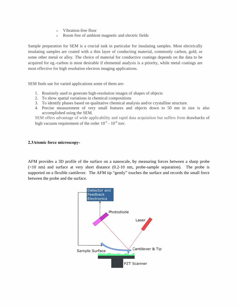
Fig 6. Block diagram of AFM
The probe is placed on the end of a cantilever (which one can think of as a spring). The
amount of force between the probe and is dependent on the spring constant (stiffness of the cantilever and the distance between the probe and the sample surface. This force can be described using Hooke’s Law: ample)
F=-k·x
F = Force
k = spring constant
x = cantilever deflection
If the spring constant of cantilever (typically ~ 0.1-1 N/m) is less than surface, the cantilever bends and deflection is monitored. Probes are typically made from Si3N4, or Si. Different cantilever lengths, materials, and shapes allow for varied spring constants and resonant frequencies. The motion of the probe across the surface is controlled using feedback loop and piezoelectronic scanners.There are 3 primary imaging modes in AFM-
(1) Contact AFM (< 0.5 nm probe-surface separation)
When cantilever bends are due to sample interaction the force on the tip is repulsive. By maintaining a constant cantilever deflection (using the feedback loops) the force between the probe and the sample remains constant and an image of the surface is obtained.
Advantages: fast scanning, good for rough samples, used in friction analysis
Disadvantages: at time forces can damage/deform soft samples (however imaging in liquids often resolves this issue)
(2) Intermittent contact (0.5-2 nm probe-surface separation)
However, in this mode the cantilever is oscillated at its resonant frequency, Figure 4. The probe lightly “taps” on the sample surface during scanning, contacting the surface at the bottom of its swing. By maintaining constant oscillation amplitude a constant tip-sample interaction is maintained and an image of the surface is obtained.
Advantages: allows high resolution of samples that are easily damaged and/or loosely held to a surface; good for biological samples
Disadvant
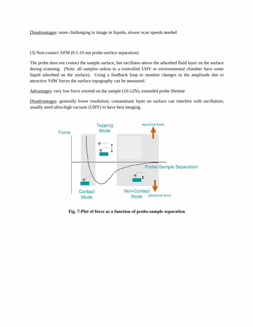
(3) Non-c
The probeduring scaliquid adsattractive
Advantag
Disadvantusually ne
tages: more c
contact AFM
e does not conanning. (Nosorbed on thVdW forces
ges: very low
tages: generaeed ultra-high
F
challenging to
(0.1-10 nm pr
ntact the sampte: all samplee surface). Uthe surface to
force exerted
ally lower resh vacuum (UH
Fig. 7-Plot of
o image in liqu
robe-surface
ple surface, bes unless in aUsing a feed
opography can
d on the sampl
solution; contHV) to have b
force as a fu
uids, slower s
separation)
but oscillates aa controlled Udback loop ton be measure
le (10-12N), e
taminant layebest imaging.
nction of pro
scan speeds n
above the adsUHV or envio monitor chd.
extended prob
er on surface
obe-sample s
needed
sorbed fluid laironmental ch
hanges in the
be lifetime
e can interfer
separation
ayer on the suhamber have e amplitude d
re with oscill
urface some
due to
lation;
3. Spectroscopy
3.1 UV-Visible spectroscopy
The word ‘spectroscopy’ is used as a collective term for all the analytical techniques based on the interaction of light and matter. Spectrophotometry is one of the branches of spectroscopy where we measure the absorption of light by molecules that are in a gas or vapour state or dissolved molecules/ions. Spectrophotometry investigates the absorption of the different substances between the wavelength limits 190 nm and 780 nm (visible spectroscopy is restricted to the wavelength range of electromagnetic radiation detectable by the human eye, that is above ~360 nm; ultraviolet spectroscopy is used for shorter wavelengths). In this wavelength range the absorption of the electromagnetic radiation is caused by the excitation (i.e. transition to a higher energy level) of the bonding and non-bonding electrons of the ions or molecules. A graph of absorbance against wavelength gives the sample’s absorption spectrum.
Spectrophotometry is used for both qualitative and quantitative investigations of samples. The wavelength at the maximum of the absorption band gives information about the structure of the molecule or ion and the extent of the absorption is proportional with the amount of the species absorbing the light.
Quantitative measurements are based on Beer’s Law which is described as follows:
A = c l
Where; A-absorbance [A = log10 (I0/I), I0 is the incident light’s intensity and I is the light intensity after it passes through the sample];
e- Molar absorbance or absorption coefficient [in dm3 mol-1 cm-1 units];
c- Concentration (molarity) of the compound in the solution [in moldm-3 units];
l - Path length of light in the sample [in cm units].
The instruments used for spectrophotometry are called photometers and Spectrophotometers. The difference between them is that we can only make measurements at a particular wavelength with a photometer, but spectrophotometers can be used for the whole wavelength range. Both types of instruments have suitable light sources, monochromator (that selects the light with the necessary wavelength) and a detector. The solution is put into a sample tube (called a “cuvette”). The light intensity

measured the readou
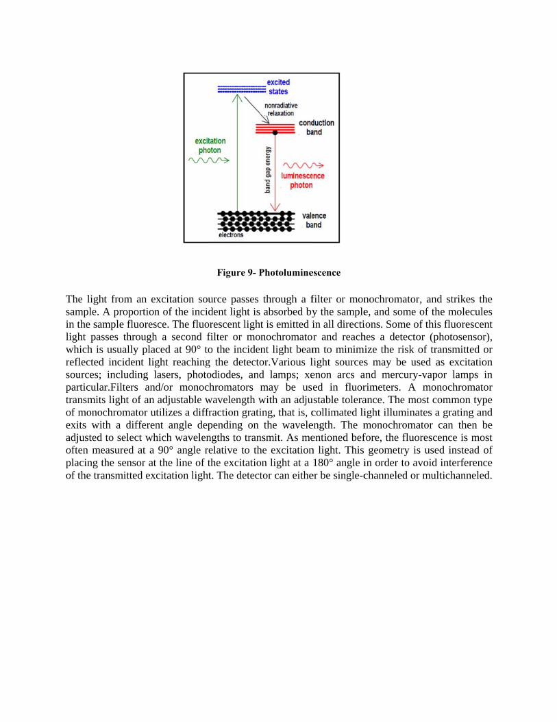
3.2 P
Photolumstructure othe matersample isluminesceis a direct
Photo-excelectrons light (a r(photolumthe transitis related determina
by the detecut (Fig.8)
Photolumines
minescence spof materials. Lrial in a proces through thence is calledt measure of v
citation causereturn to theiradiative pro
minescence) retion between to the relativ
ation particula
ctor is convert
Fi
scence spectr
pectroscopy iLight is direcess called phhe emission d photoluminevarious impor
es electrons wir equilibriumocess) or maelates to the dthe excited stve contributioarly in case of
ted into an el
igure 8- UV/V
roscopy
is a contactlcted onto a samhoto-excitation
of light, orescence. The rtant material
within the matm states, the exay not (a nodifference in tate and the eon of the radf semiconduc
lectric signal
Vis spectrop
less, nondestmple, where in. One way tr luminescenintensity andproperties.
terial to movexcess energy onradiative penergy levels
equilibrium stdiative procesctors.
and is displa
hotometer
tructive methit is absorbedthis excess e
nce. In the d spectral con
e into permissis released a
process). Thes between thetate (Fig.9). Tss. Photolumi
ayed as a cert
hod of probid and imparts energy can becase of pho
ntent of this p
sible excited and may inclue energy of e two electronThe quantity oinescence is
tain absorban
ing the elecexcess energ
e dissipated boto-excitationphotolumines
states. Whenude the emissi
the emitted n states involvof the emittedused for ban
nce on
tronic gy into by the n, this scence
these ion of
light ved in d light nd gap
The lightsample. Ain the samlight paswhich is reflected sources; particulartransmitsof monocexits witadjusted often meplacing thof the tra
t from an exA proportionmple fluoressses through
usually placincident ligincluding l
r.Filters ands light of an chromator utth a differento select wh
easured at a he sensor at
ansmitted exc
xcitation soun of the incidsce. The fluoh a second fced at 90° toght reachinglasers, photod/or monocadjustable wtilizes a diffnt angle dephich wavelen90° angle rthe line of t
citation light
Figure 9- P
urce passes dent light is
orescent lightfilter or moo the incideng the detectoodiodes, andchromators mwavelength wfraction gratipending on ngths to tranelative to ththe excitatiot. The detect
Photolumine
through a fabsorbed by
t is emitted inochromatont light beamor.Various ld lamps; xemay be uswith an adjuing, that is, cthe wavele
nsmit. As mehe excitationon light at a tor can eithe
escence
filter or mony the samplein all directir and reachm to minimilight sourcesenon arcs aed in fluor
ustable toleracollimated liength. The mentioned befn light. This 180° angle i
er be single-c
nochromatore, and some ions. Some ohes a detectoize the risk s may be u
and mercuryrimeters. A ance. The moight illuminamonochromafore, the fluo
geometry iin order to achanneled or
r, and strikeof the mole
of this fluoreor (photosenof transmittsed as excit
y-vapor lampmonochrom
ost commonates a gratingator can theorescence is s used inste
avoid interferr multichann
es the ecules escent nsor), ted or tation ps in mator n type g and en be most ad of rence
neled.