Embed Size (px)
DESCRIPTION
Characterization of Sputtered Inconel 617
Citation preview
J O U R N A L OF M A T E R I A L S S C I E N C E 25 (1990) 144-148
Characterization of sputtered Inconel 617 Part 2 Coatings in cross-section
M A R I O E M I L I A N I Pratt and Whitney, PO Box 109600, MS 707-28, West Palm Beach, Florida 33410, USA
M A R C R I C H M A N Division of Engineering, Brown University, Box D, Providence, Rhode Island 02913, USA
R I C H A R D BROWN Department of Chemical Engineering, University of Rhode Island, Kingston, Rhode Island 02881, USA
Inconel 617 coatings, 1 0 to 13#m thick, were r.f. magnetron sputtered on to commercially pure a-titanium substrates without external bias or heat and examined in the as-deposited condition by analytical transmission electron microscopy (TEM). Coatings were an f cc solid solution with an average lattice parameter of 0.366nm and had a (1 1 1) preferred orientation. Examination of the microstructure in cross-section showed it consisted of columnar grains on average 60nm wide, and contained a high density of twins and stacking faults parallel to the substrate. Comparison with sputtered copper and nickel coatings indicate that the stacking fault energy of sputtered Inconel 617 is similar to that of pure copper.
1. I n t r o d u c t i o n Incone1617 (UNS N00617) is a nickel-based superalloy used in high-temperature environments (~ 1000~ due to its excellent mechanical stability, oxidation, and corrosion resistance. This alloy is a face-centred cubic solid solution of nickel (52%), chromium (22 wt %), cobalt (12 wt %), and molybdenum (9 wt %), with small amounts ( < 1.5 wt % each) of iron, silicon, titanium and aluminium [1]. The microstructure of sol- ution annealed in Inconel 617 consists of equiaxed 7 grains 65 #m average diameter or coarser, with grain boundary M23C 6 (M = Cr, Me) and intragranular MC carbides (M = Ti). Bulk Inconel 617 is not 7' strengthened in the solution-annealed condition, but will undergo slight strengthening after lengthy expo- sure to temperatures above 650~ primarily due to precipitation of intragranular M23C 6 (M = Cr + Me) [2]. No topologically close packed (tcp) phases such as a, Z, or # have been identified [2, 3].
The as-sputtered microstructure of Inconel 617 found in this study is similar to other sputtered tran- sition metals, particularly copper and nickel [4-6, 8, 10]. Thick (0.1 to 1.0ram) copper coatings d.c. sput- tered at approximately 600nmmin -1 on to copper and aluminium substrates maintained at -196 to 13 ~ C with biases of - 20 to - 75 V, respectively, were examined in both plan (through thickness) and cross- section by transmission electron microscopy (TEM) [4]. The gain size (or equivalently, column width) was found to depend upon substrate temperature and bias. For example, coatings in plan section deposited at 6~ and - 7 5 V bias had a bimodal distribution of equiaxed grains ranging in diameter from 250 to 1000nm, with some randomly oriented twins and
stacking faults perpendicular to the substrate. Cross- sections showed long columnar grains perpendicular to the substrate which contained a high density of twins and stacking faults parallel to the substrate. Columnar grains were fc c with a (111) orientation, indicating that the most densely packed atom planes are parallel to the substrate.
In contrast, coatings deposited on to substrates maintained at temperatures up to 13~ recrystallized at or below room temperature resulting in a (100) orientation parallel to the substrate. This behaviour has been found in other studies of vacuum-deposited copper coatings [5, 6], and is attributed to intrinsic coating stress and a high, non-equilibrium, concen- tration of vacancies formed during sputter deposition at a low homologous temperature (T/TM). These pro- vide the driving force for dislocation climb, and were found to be sensitive to substrate bias and impurities in the coating [6].
The high density of twins and stacking faults in columnar grains of vacuum-deposited fcc coatings are generated as follows [4]. Atoms impinging upon
the substrate compete for favourable close-packed positions on densely packed (111) planes, but not all are incorporated into the (111) orientation. Atoms that cannot be accommodated will still deposit as close-packed planes and produce planar defects (stacking faults) which may form the mirror plane required for twins. Subsequent addition of sputtered atoms on to new orientations produces twins of measureable thickness. Stacking faults may also be formed by shear stresses across (111) planes due to impingement of columnar grains during growth of the coating.
1 44 0022-2461/90 $03.00 + .12 �9 1990 Chapman and Hall Ltd.
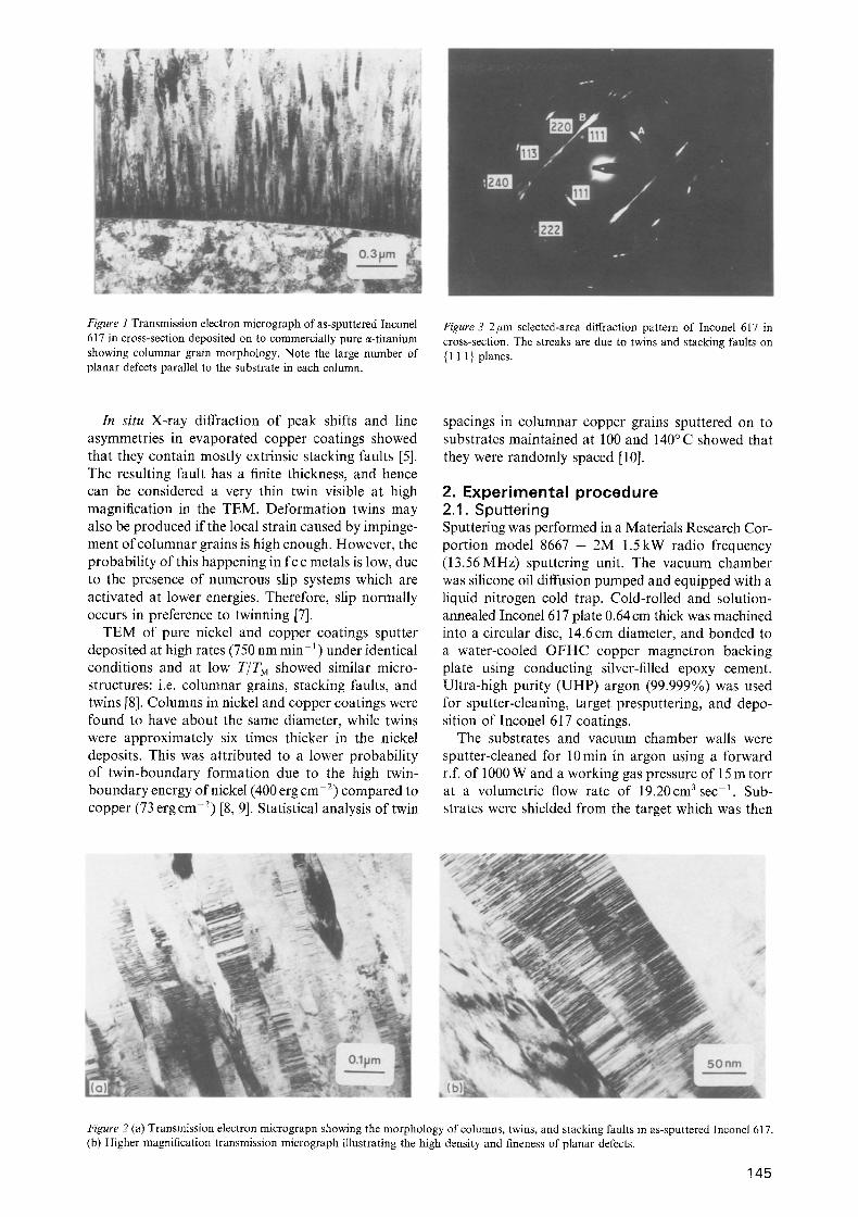
Figure 1 Transmission electron micrograph of as-sputtered Inconel 617 in cross-section deposited on to commercially pure a-titanium showing columnar grain morphology. Note the large number of planar defects parallel to the substrate in each column.
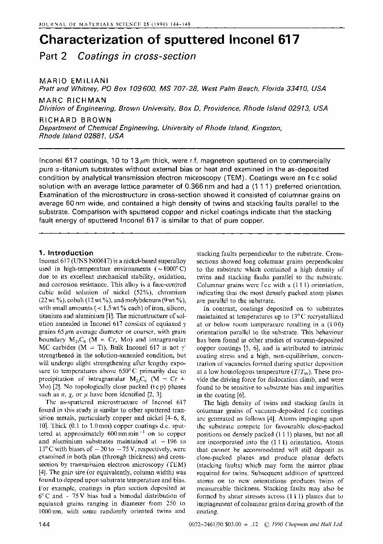
Figure 3 2/~m selected-area diffraction pattern of Inconel 617 in cross-section. The streaks are due to twins and stacking faults on {111} planes.
In situ X-ray diffraction of peak shifts and line asymmetries in evaporated copper coatings showed that they contain mostly extrinsic stacking faults [5]. The resulting fault has a finite thickness, and hence can be considered a very thin twin visible at high magnification in the TEM. Deformation twins may also be produced if the local strain caused by impinge- ment of columnar grains is high enough. However, the probability of this happening in fc c metals is low, due to the presence of numerous slip systems which are activated at lower energies. Therefore, slip normally occurs in preference to twinning [7].
TEM of pure nickel and copper coatings sputter deposited at high rates (750 nm min- 1 ) under identical conditions and at low T/TM showed similar micro- structures: i.e. columnar grains, stacking faults, and twins [8]. Columns in nickel and copper coatings were found to have about the same diameter, while twins were approximately six times thicker in the nickel deposits. This was attributed to a lower probability of twin-boundary formation due to the high twin- boundary energy of nickel (400 erg cm 2) compared to copper (73 erg cm -2) [8, 9]. Statistical analysis of twin
spacings in columnar copper grains sputtered on to substrates maintained at 100 and 140~ showed that they were randomly spaced [10].
2. Experimental procedure 2.1. S p u t t e r i n g Sputtering was performed in a Materials Research Cor- portion model 8667 -t- 2M 1.5kW radio frequency (13.56MHz) sputtering unit. The vacuum chamber was silicone oil diffusion pumped and equipped with a liquid nitrogen cold trap. Cold-rolled and solution- annealed Inconel 617 plate 0.64 cm thick was machined into a circular disc, 14.6 cm diameter, and bonded to a water-cooled OFHC copper magnetron backing plate using conducting silver-filled epoxy cement. Ultra-high purity (UHP) argon (99.999%) was used tbr sputter-cleaning, target presputtering, and depo- sition of Inconel 617 coatings.
The substrates and vacuum chamber walls were sputter-cleaned for 10min in argon using a forward r.f. of 1000 W and a working gas pressure of 15 m torr at a volumetric flow rate of 19.20cm 3 sec -1. Sub- strates were shielded from the target which was then
Figure 2 (a) Transmission electron micrograpn showing the morphology of columns, twins, and stacking faults in as-sputtered Inconel 617. (b) Higher magnification transmission micrograph illustrating the high density and fineness of planar defects.
145
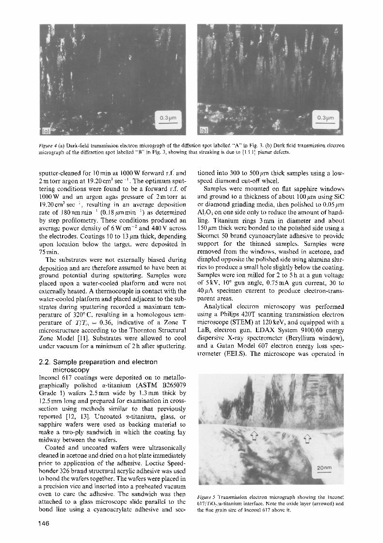
Figure 4 (a) Dark-field transmission electron micrograph of the diffusion spot labelled "A" in Fig. 3. (b) Dark field transmission electron micrograph of the diffraction spot labelled "B" in Fig. 3, showing that streaking is due to {1 1 1} planar defects.
sputter-cleaned for 10 rain at 1000 W forward r.fl and 2 m torr argon at 19.20 cm 3 sec -~ . The optimum sput- tering conditions were found to be a forward r.f. of 1000W and an argon agas pressure of 2 m t o r r at 19.20cm 3 sec -1, resulting in an average deposition rate of 180 nm rain- 1 (0.18 #m min- 1 ) as determined by step profilometry. These conditions produced an average power density of 6 W cm -2 and 440 V across the electrodes. Coatings 10 to 13 #m thick, depending upon location below the target, were deposited in 75 rain.
The substrates were not externally biased during deposition and are therefore assumed to have been at ground potential during sputtering. Samples were placed upon a water-cooled platform and were not externally heated. A thermocouple in contact with the water-cooled platform and placed adjacent to the sub- strates during sputtering recorded a maximum tem- perature of 320 ~ C, resulting in a homologous tem- perature of T/Tm = 0.36, indicative of a Zone T microstructure according to the Thornton Structural Zone Model [11]. Substrates were allowed to cool under vacuum for a minimum of 2 h after sputtering.
2.2. Sample preparation and electron microscopy
Inconel 617 coatings were deposited on to metallo- graphically polished e-titanium (ASTM B265079 Grade 1) wafers 2.5ram wide by 1.3ram thick by 12.5 mm long and prepared for examination in cross- section using methods similar to that previously reported [12, 13]. Uncoated e-titanium, glass, or sapphire wafers were used as backing material to make a two-ply sandwich in which the coating lay midway between the wafers.
Coated and uncoated wafers were ultrasonically cleaned in acetone and dried on a hot plate immediately prior to application of the adhesive. Loctite Speed- bonder 326 brand structural acrylic adhesive was used to bond the wafers together. The wafers were placed in a precision vice and inserted into a preheated vacuum oven to cure the adhesive. The sandwich was then attached to a glass microscope slide parallel to the bond line using a cyanoacrylate adhesive and sec-
146
tioned into 300 to 500 #m thick samples using a low- speed diamond cut-off wheel.
Samples were mounted on flat sapphire windows and ground to a thickness of about 100 #m using SiC or diamond grinding media, then polished to 0.05 #m A1203 on one side only to reduce the amount of hand- ling. Titanium rings 3ram in diameter and about 150/~m thick were bonded to the polished side using a Sicomet 50 brand cyanoacrylate adhesive to provide support for the thinned samples. Samples were removed from the windows, washed in acetone, and dimpled opposite the polished side using alumina slur- ries to produce a small hole slightly below the coating. Samples were ion milled for 2 to 5 h at a gun voltage of 5kV, 10 ~ gun angle, 0.75mA gun current, 30 to 40/~A specimen current to produce electron-trans- parent areas.
Analytical electron microscopy was performed using a Philips 420T scanning transmission electron microscope (STEM) at 120 keV, and equipped with a LaB 6 electron gun, EDAX System 9100/60 energy dispersive X-ray spectrometer (Beryllium window), and a Gatan Model 607 electron energy loss spec- trometer (EELS). The microscope was operated in
Figure 5 Transmission electron micrograph showing the Inconel 617/TiO2/c~-titanium interface. Note the oxide layer (arrowed) and the fine grain size of Inconel 617 above it.
TEM mode and aligned prior to each use to ensure reproducible conditions for magnification, diffraction camera length, and energy dispersive microanalysis.
3. Resu l ts and d iscuss ion 3.1. TEM of as-sputtered Inconel 617
coatings The microstructure of sputtered Inconel 617 in cross- section was found to consist of long columnar 7 grains 20 to 150 nm wide perpendicular to the substrate, as shown in Fig. 1. Some grains appear to have nucleated from within the coating, but are instead likely to have not fully intersected the plane of the micrograph. Therefore, most columnar grains grew continuously from the substrate. No M23C 6 n o r TiC precipitates were found in as-sputtered coatings. The column width remained relatively constant and was generally not found to increase with distance from the substrate. While the experimentally determined homologous temperature indicates the structure is Zone T, direct imaging by TEM shows the as-deposited microstruc- ture is, in fact, better characterized as Zone 2 due to the absence of shadowing effects [11].
A high density of twins and stacking faults parallel to the substrate were also found, and they ranged in thickness from about 1.5 to 50nm (Figs 2a and b). Selected-area diffraction (Fig. 3) showed that the coat- ings are highly textured and contain streaks. Dark- field imaging of streaked and unstreaked fcc (1 1 1) reflections confirmed that streaking was due to (1 1 1) twins and stacking faults (Figs 4a and b). Stereological analysis showed that there were 16 to 18 columns per micrometre parallel to the substrate, and their average diameter was about 60 nm. This is consistent with the
average grain size found in plan sections [14]. In con- trast, computer modelling of Zone 2 columnar growth in vapour-deposited coatings has shown that the average grain size (or column width) increases with distance from the substrate [15].
The high density of twins and stacking faults paral- lel to the substrate (Fig. 2b), coupled with overlapping grains and strain contrast, made it difficult to perform accurate stereological analysis. Most twins and stack- ing faults had thicknesses ranging from 1 to 15nm, with the majority less than 30nm thick, and 30 to 100nm wide. The average linear density of planar defects is then about 500 per micrometer. Because plan sections represent parallel slices through twins and stacking faults which each appear as a single grain, the total interfacial area is approxi- mately 1000 times greater than the grain-boundary area, resulting in a total of about 3.2 x 109cm2cm -3 [14].
The morphology of as-sputtered Inconel 617 and the mechanism of columnar growth appear to be in good agreement with previous studies [4, 8, 10]. How- ever, TEM studies of the morphology of twins and stacking faults in sputtered copper and nickel coatings showed that the density of planar defects is greater in copper coatings, whereas twins were about six times thicker in nickel coatings [8, 10]. Inconel 617 coatings, which contain about 52% nickel, had a high density of planar defects, and therefore, stacking fault energy more like that found in sputtered copper coatings [8, 9]. The low interfacial energy in Inconel 617 is believed to be related to deposition parameters specific to the present study and the presence of alloying elements.
tO S
s ~7 5 6
2 I 8
SCALE FACTORe OFFSET=78,S74, 8,888 L I t I, h I I
Cr
Cr
CSUHTS/SEC BU=5,SSkU SI=@,SSSS pm I I I L I I I I i I I
J• i [ I I i i i 1 i i i i I I
(a) KIMETIC EiIER@Y
SCALE 18
9
I
'0_]
(b)
Ni
FACTORj OFFSET=8,497, 8,~88 i~ COUHTS/SEC BV=5,98kU BI=g,8088 IIA I I I I I I I I i , I I I I ~ . 1 f I i J
�9 / I
Ti O f "
i i i
e,, 'B.6 '1,3 i / I i
h6 1,9 ~UTTER TNE (rnin)
2. 2, 2,9 3,2
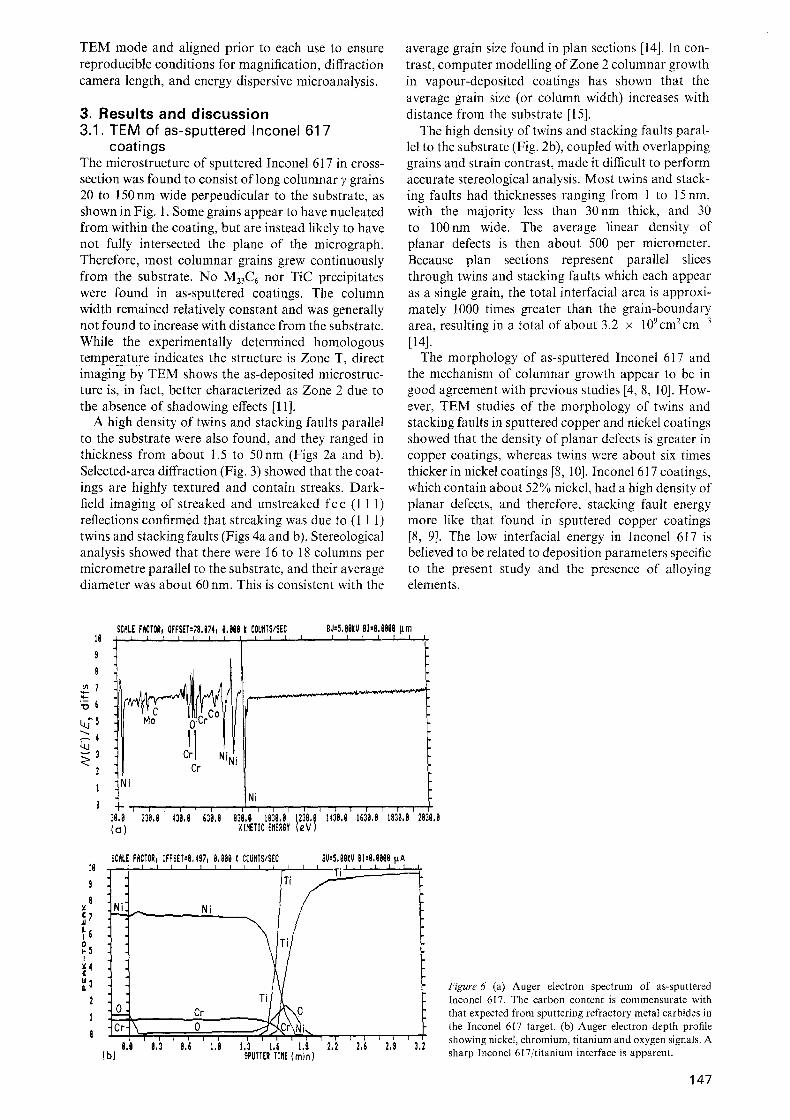
Figure 6 (a) Auger electron spectrum of as-sputtered Inconel 617. The carbon content is commensurate with that expected from sputtering refractory metal carbides in the Inconel 617 target. (b) Auger electron depth profile showing nickel, chromium, titanium and oxygen signals. A sharp Inconel 617/titanium interface is apparent.
147
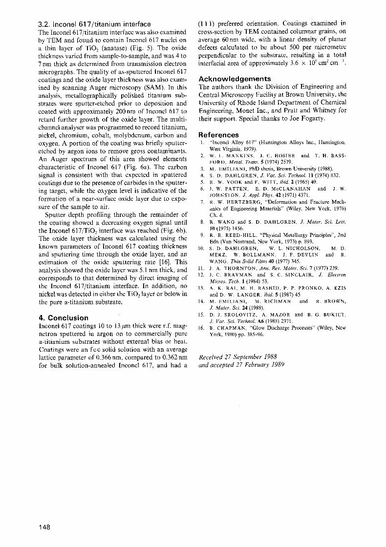
3.2. Inconel 617/titanium interface The Inconel 617/titanium interface was also examined by TEM and found to contain Inconel 617 nuclei on a thin layer of TiO2 (anatase) (Fig. 5). The oxide thickness varied from sample-to-sample, and was 4 to 7 nm thick as determined from transmission electron micrographs. The quality of as-sputtered Inconel 617 coatings and the oxide layer thickness was also exam- ined by scanning Auger microscopy (SAM). In this analysis, metallographically polished titanium sub- strates were sputter-etched prior to deposition and coated with approximately 200nm of Inconel 617 to retard further growth of the oxide layer. The multi- channel analyser was programmed to record titanium, nickel, chromium, cobalt, molybdenum, carbon and oxygen. A portion of the coating was briefly sputter- etched by argon ions to remove gross contaminants. An Auger spectrum of this area showed elements characteristic of Inconel 617 (Fig. 6a). The carbon signal is consistent with that expected in sputtered coatings due to the presence of carbides in the sputter- ing target, while the oxygen level is indicative of the formation of a near-surface oxide layer due to expo- sure of the sample to air.
Sputter depth profiling through the remainder of the coating showed a decreasing oxygen signal until the Inconel 617/TIO2 interface was reached (Fig. 6b). The oxide layer thickness was calculated using the known parameters of Inconel 617 coating thickness and sputtering time through the oxide layer, and an estimation of the oxide sputtering rate [16]. This analysis showed the oxide layer was 5.1 nm thick, and corresponds to that determined by direct imaging of the Inconel 617/titanium interface. In addition, no nickel was detected in either the TiO2 layer or below in the pure c~-titanium substrate.
4. Conclusion Inconel 617 coatings 10 to 13/~m thick were r.f. mag- netron sputtered in argon on to commercially pure c~-titianium substrates without external bias or heat. Coatings were an fc c solid solution with an average lattice parameter of 0.366 nm, compared to 0.362 nm for bulk solution-annealed Inconel 617, and had a
(1 1 1) preferred orientation. Coatings examined in cross-section by TEM contained columnar grains, on average 60 nm wide, with a linear density of planar defects calculated to be about 500 per micrometre perpendicular to the substrate, resulting in a total interfacial area of approximately 3.6 x 10⁹ c m 2 c m -3 .
Acknowledgements The authors thank the Division of Engineering and Central Microscopy Facility at Brown University, the University of Rhode Island Department of Chemical Engineering, Monet Inc., and Pratt and Whitney for their support. Special thanks to Joe Fogarty.
References 1. "Inconel Alloy 617" (Huntington Alloys Inc., Huntington,
West Virginia, 1979). 2. W. L. MANKINS, J. C. HOSIER and T. H. BASS-
FORD, Metal. Trans. 5 (1974) 2579. 3. M. EMILIANI, PhD thesis, Brown University (1988). 4. S. D. DAHLGREN, J. Vac. Sci. Technol. 11 (1974) 832. 5. R. W. VOOK and F. WITT, ibid. 2 (1965) 49. 6. J. W. PATTEN, E . D . McCLANAHAN and J . W .
JOHNSTON, J. Appl. Phys. 42 (1971) 4371. 7. R. W. HERTZBERG, "Deformation and Fracture Mech-
anics of Engineering Materials" (Wiley, New York, 1976) Ch. 4.
8. R. WANG and S. D. DAHLGREN, J. Mater. Sci. Lett. 10 (1975) 1456.
9. R. E. REED-HILL, "Physical Metallurgy Principles", 2nd Edn (Van Nostrand, New York, 1973) p. 893.
10. s. D. DAHLGREN, W . L . NICHOLSON, M . D . MERZ, W. BOLLMANN, J . F . DEVLIN and R. WANG, Thin Solid Films 40 (1977) 345.
11. J. A. THORNTON, Ann. Rev. Mater. Sci. 7 (1977) 239. 12. J. C. BRAVMAN and S. C. SINCLAIR, J. Electron
Micros. Tech. I (1984) 53. 13. A. K. RAI, M. H. RASHID, P. P. PRONKO, A. EZIS
and D. W. LANGER, ibid. 5 (1987) 45. 14. M. EMILIANI, M. RICHMAN and R. BROWN,
J. Mater. Sci. 24 (1989). 15. D. J. SROLOVITZ, A. MAZOR and B. G. BUKIET,
J. Vac. Sci. Teehnol. A6 (1988) 2371. 16. B. CHAPMAN, "Glow Discharge Processes" (Wiley, New
York, 1980) pp. 385-96.
Received 27 September 1988 and aecepted 27 February 1989
148